Embed Size (px)
Citation preview
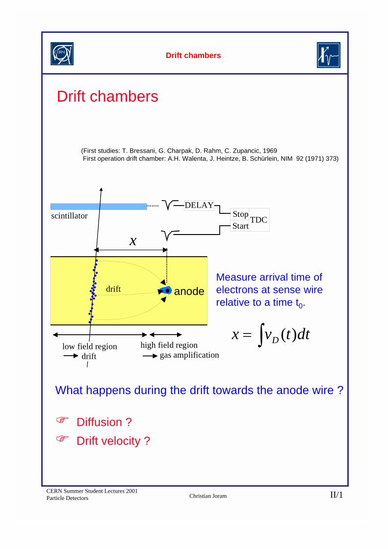
CERN Summer Student Lectures 2001Particle Detectors Christian Joram II/1
Drift chambers
Measure arrival time ofelectrons at sense wirerelative to a time t0.
anode
TDCStartStop
DELAYscintillator
drift
low field region drift
high field region gas amplification
Drift chambers
What happens during the drift towards the anode wire ?
� Diffusion ?� Drift velocity ?
(First studies: T. Bressani, G. Charpak, D. Rahm, C. Zupancic, 1969 First operation drift chamber: A.H. Walenta, J. Heintze, B. Schürlein, NIM 92 (1971) 373)
dttvx D )(��
x
CERN Summer Student Lectures 2001Particle Detectors Christian Joram II/2
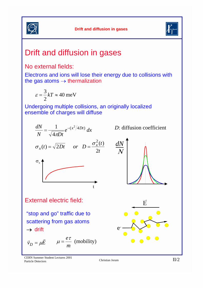
Drift and diffusion in gases
Drift and diffusion in gasesNo external fields:Electrons and ions will lose their energy due to collisions withthe gas atoms � thermalization
Undergoing multiple collisions, an originally localizedensemble of charges will diffuse
ttDorDtt
dxeDtN
dN
xx
Dtx
2)( 2)(
41
2
)4( 2
��
�
��
�� D: diffusion coefficient
meV4023
�� kT�
t
�x
dN�
External electric field:
e-
�
EvD�
�
�� (mobility)
me�
� �
“stop and go” traffic due to scattering from gas atoms���� drift
CERN Summer Student Lectures 2001Particle Detectors Christian Joram II/3
Drift and diffusion in gases
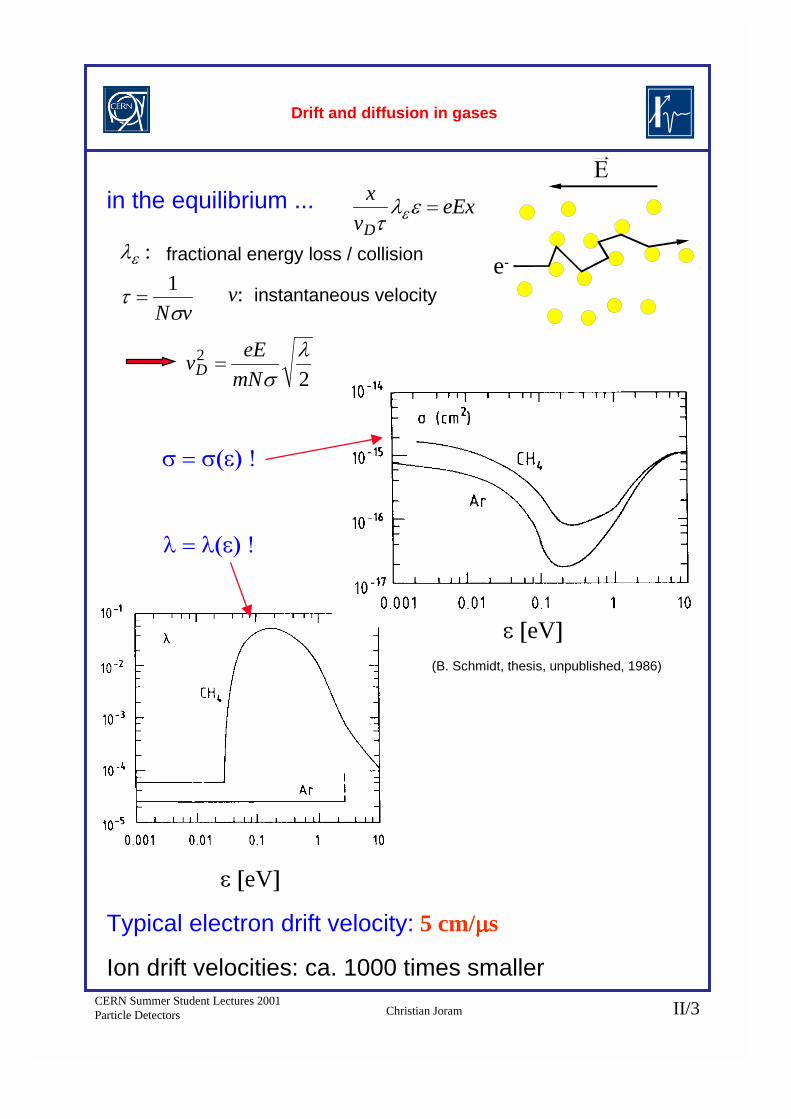
in the equilibrium ... eExv
xD
����
�
e-
�
:�
� fractional energy loss / collision
vN��
1� v: instantaneous velocity
22 �
�mNeEvD �
���eV�
���eV�
���������
�������
(B. Schmidt, thesis, unpublished, 1986)
Typical electron drift velocity: 5 cm/����s
Ion drift velocities: ca. 1000 times smaller
CERN Summer Student Lectures 2001Particle Detectors Christian Joram II/4
Drift and diffusion in gases
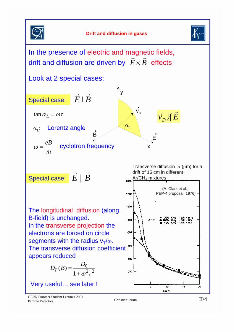
In the presence of electric and magnetic fields,drift and diffusion are driven by effectsBE
��
�
x
y
EB
vD
�L
��� �Ltan
Special case:
�L: Lorentz angle
BE��
�
mBe�
�� cyclotron frequency
EvD
�
� ||
BE��
||Special case:
The longitudinal diffusion (alongB-field) is unchanged.In the transverse projection theelectrons are forced on circlesegments with the radius vT/�.The transverse diffusion coefficientappears reduced
220
1)(
���
�DBDT
Transverse diffusion � (�m) for adrift of 15 cm in differentAr/CH4 mixtures
(A. Clark et al., PEP-4 proposal, 1976)
Very useful… see later !
Look at 2 special cases:
CERN Summer Student Lectures 2001Particle Detectors Christian Joram II/5
Drift chambers
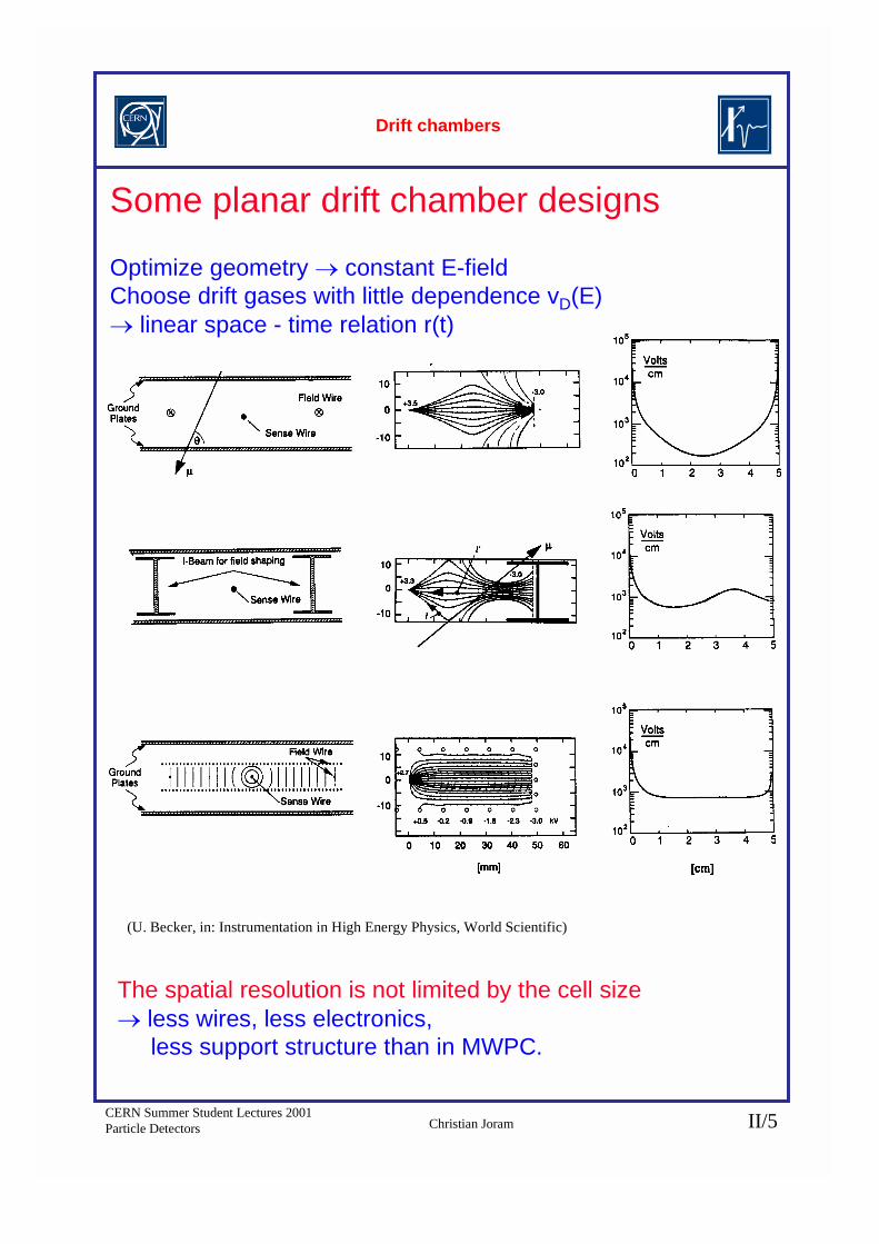
Some planar drift chamber designs
Optimize geometry � constant E-field Choose drift gases with little dependence vD(E)� linear space - time relation r(t)
(U. Becker, in: Instrumentation in High Energy Physics, World Scientific)
The spatial resolution is not limited by the cell size� less wires, less electronics, less support structure than in MWPC.
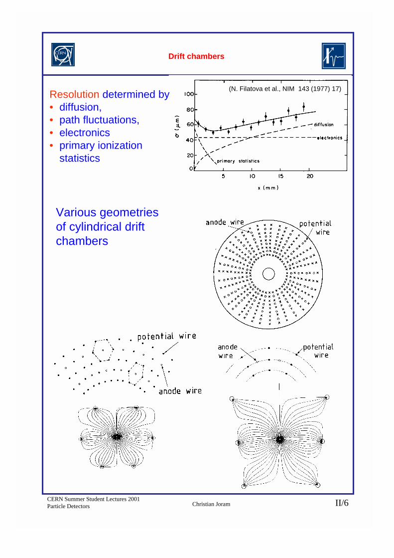
CERN Summer Student Lectures 2001Particle Detectors Christian Joram II/6
Drift chambers
Various geometriesof cylindrical driftchambers
Resolution determined by• diffusion,• path fluctuations,• electronics• primary ionization
statistics
(N. Filatova et al., NIM 143 (1977) 17)
CERN Summer Student Lectures 2001Particle Detectors Christian Joram II/7
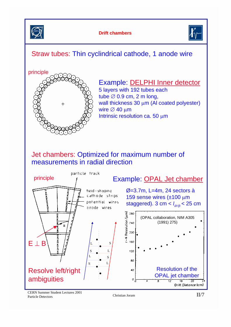
Drift chambers
Straw tubes: Thin cyclindrical cathode, 1 anode wire
Jet chambers: Optimized for maximum number ofmeasurements in radial direction
Example: DELPHI Inner detector5 layers with 192 tubes eachtube � 0.9 cm, 2 m long,wall thickness 30 �m (Al coated polyester)wire � 40 �mIntrinsic resolution ca. 50 �m
principle
E � B
Example: OPAL Jet chamber
principle
Ø=3.7m, L=4m, 24 sectors à159 sense wires (±100 �mstaggered). 3 cm < ldrift < 25 cm
Resolution of theOPAL jet chamber
(OPAL collaboration, NIM A305(1991) 275)
LS
L
S
L S
L
S
Resolve left/rightambiguities
CERN Summer Student Lectures 2001Particle Detectors Christian Joram II/8
Drift Chambers
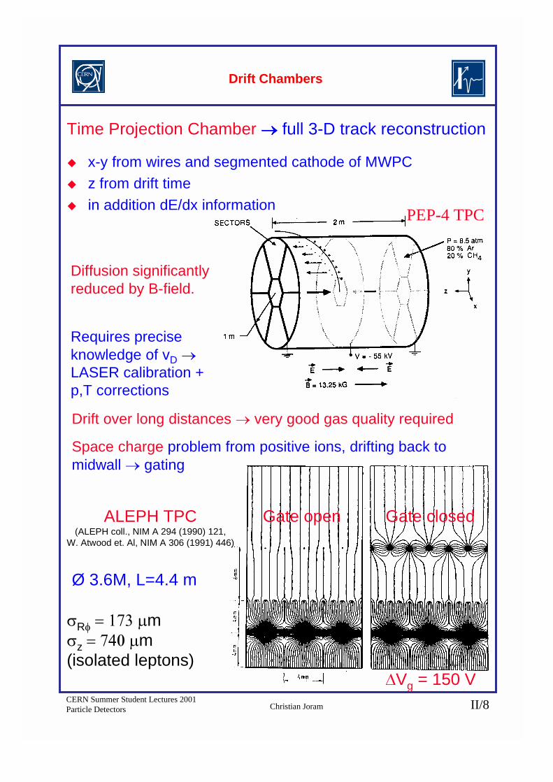
Time Projection Chamber ���� full 3-D track reconstruction
� x-y from wires and segmented cathode of MWPC� z from drift time� in addition dE/dx information PEP-4 TPC
Diffusion significantlyreduced by B-field.
Requires preciseknowledge of vD �LASER calibration +p,T corrections
Drift over long distances � very good gas quality required
Space charge problem from positive ions, drifting back tomidwall � gating
Gate open Gate closed
�Vg = 150 V
ALEPH TPC(ALEPH coll., NIM A 294 (1990) 121,
W. Atwood et. Al, NIM A 306 (1991) 446)
Ø 3.6M, L=4.4 m
�R���� ����m�z��������m(isolated leptons)
CERN Summer Student Lectures 2001Particle Detectors Christian Joram II/9
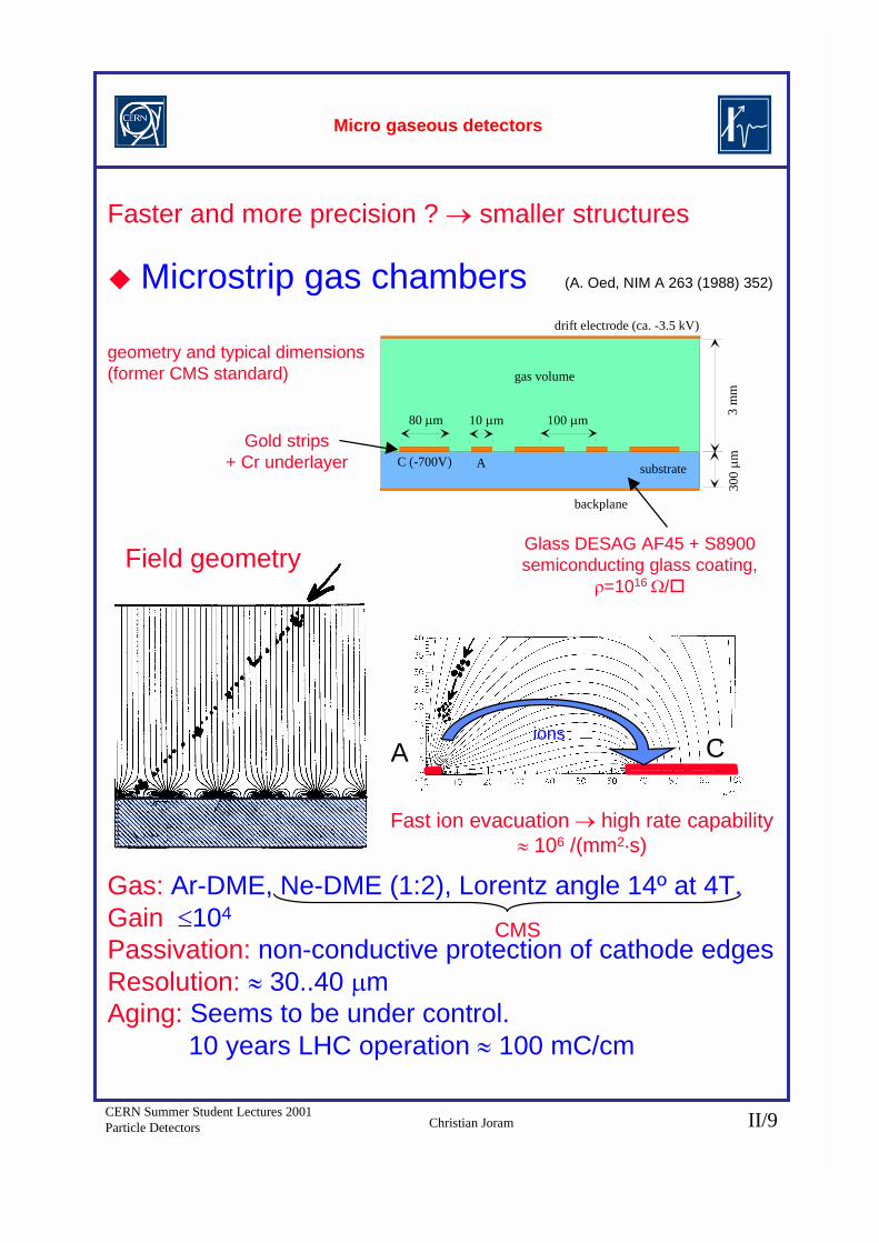
Micro gaseous detectors
Faster and more precision ? � smaller structures
� Microstrip gas chambers
80 �m 10 �m 100 �m
3 m
m
backplane
drift electrode (ca. -3.5 kV)
AC (-700V) substrate
300 �
m
gas volume
ionsA C
geometry and typical dimensions(former CMS standard)
(A. Oed, NIM A 263 (1988) 352)
Glass DESAG AF45 + S8900semiconducting glass coating,
�=1016 �/�
Gold strips+ Cr underlayer
Field geometry
Fast ion evacuation � high rate capability� 106 /(mm2�s)
Gas: Ar-DME, Ne-DME (1:2), Lorentz angle 14º at 4T. Gain ��104
Passivation: non-conductive protection of cathode edgesResolution: � 30..40 �mAging: Seems to be under control. 10 years LHC operation � 100 mC/cm
CMS
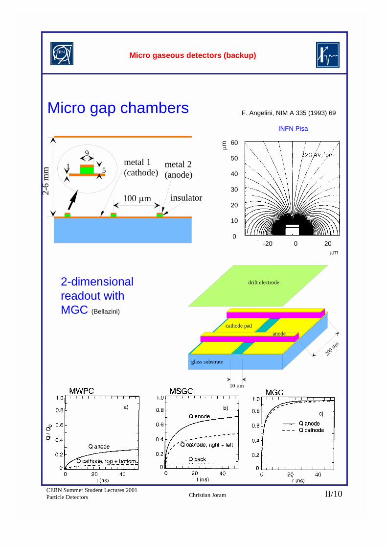
CERN Summer Student Lectures 2001Particle Detectors Christian Joram II/10
Micro gaseous detectors (backup)
Micro gap chambers
2-6
mm
100 �m
51
9metal 1(cathode)
metal 2(anode)
insulator
60
50
40
30
20
10
0
�m
�m-20 0 20
F. Angelini, NIM A 335 (1993) 69
2-dimensionalreadout withMGC (Bellazini)
200 �
mcathode pad
anode
glass substrate
10 �m
drift electrode
INFN Pisa
CERN Summer Student Lectures 2001Particle Detectors Christian Joram II/11
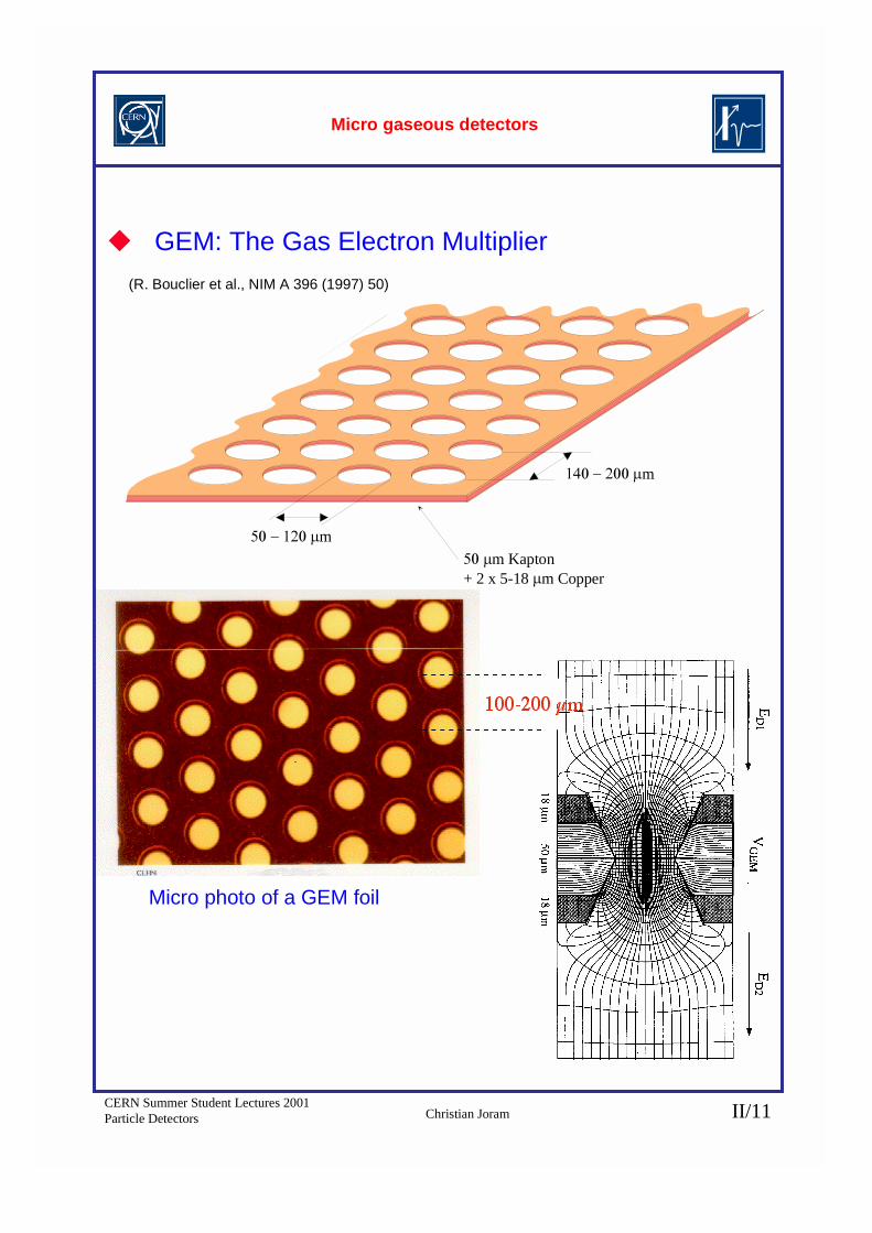
Micro gaseous detectors
� GEM: The Gas Electron Multiplier(R. Bouclier et al., NIM A 396 (1997) 50)
�����������m
����������m����m Kapton + 2 x 5-18 �m Copper
Micro photo of a GEM foil
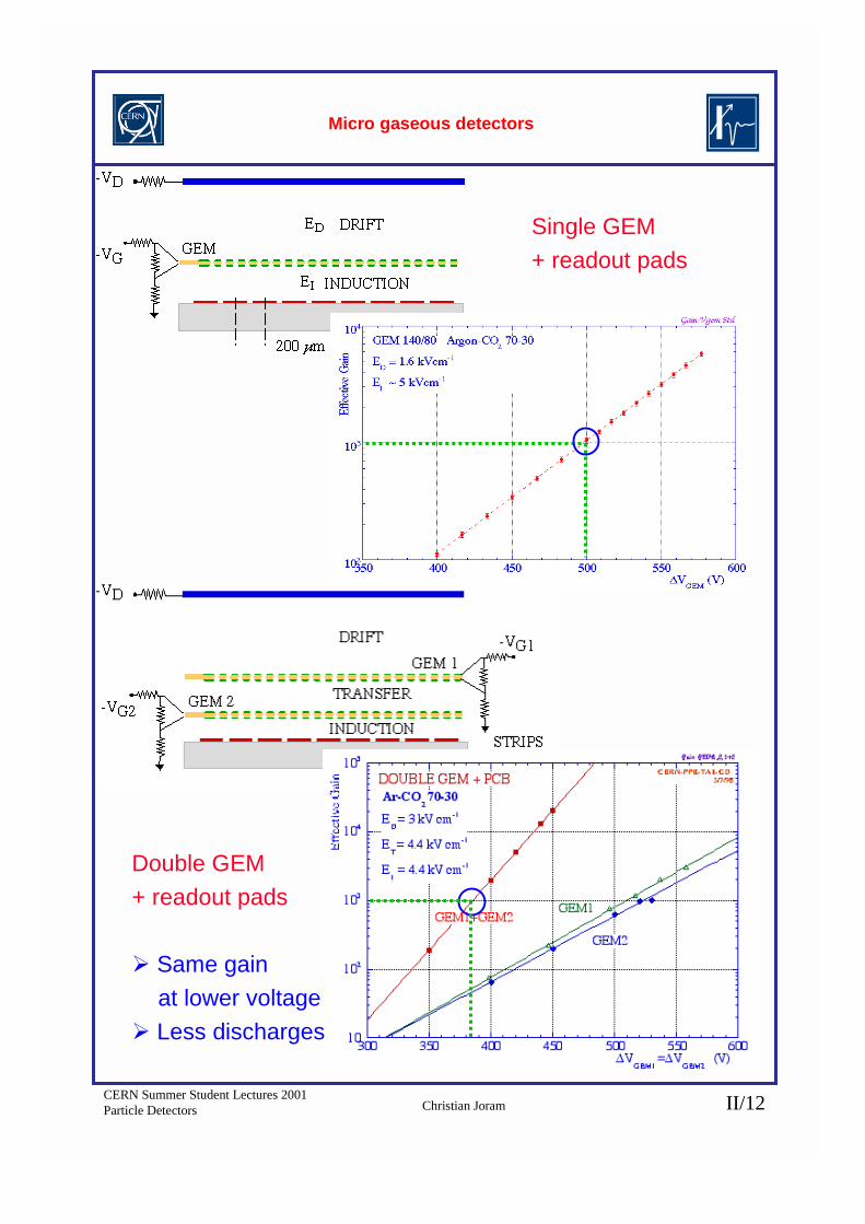
CERN Summer Student Lectures 2001Particle Detectors Christian Joram II/12
Micro gaseous detectors
Single GEM + readout pads
Double GEM+ readout pads
� Same gain at lower voltage� Less discharges
CERN Summer Student Lectures 2001Particle Detectors Christian Joram II/13
Micro gaseous detectors (backup)
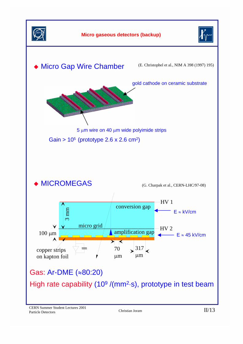
� Micro Gap Wire Chamber
� MICROMEGAS
100 �m
3 m
m
HV 1
HV 2
conversion gap
amplification gapmicro grid
copper stripson kapton foil
317 �m
70 �m
(G. Charpak et al., CERN-LHC/97-08)
E � kV/cm
E � 45 kV/cm
Gas: Ar-DME (�80:20)High rate capability (109 /(mm2�s), prototype in test beam
(E. Christophel et al., NIM A 398 (1997) 195)
gold cathode on ceramic substrate
5 �m wire on 40 �m wide polyimide strips
Gain > 105 (prototype 2.6 x 2.6 cm2)
CERN Summer Student Lectures 2001Particle Detectors Christian Joram II/14
Silicon detectors
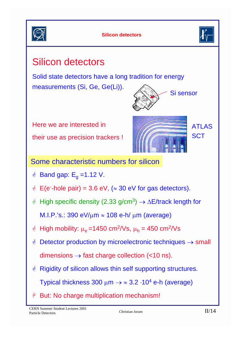
Silicon detectorsSolid state detectors have a long tradition for energymeasurements (Si, Ge, Ge(Li)).
Here we are interested in
their use as precision trackers !
� Band gap: Eg =1.12 V.
� E(e--hole pair) = 3.6 eV, (� 30 eV for gas detectors).
� High specific density (2.33 g/cm3) � �E/track length for
M.I.P.’s.: 390 eV/�m � 108 e-h/ �m (average)
� High mobility: �e =1450 cm2/Vs, �h = 450 cm2/Vs
� Detector production by microelectronic techniques � small
dimensions � fast charge collection (<10 ns).
� Rigidity of silicon allows thin self supporting structures.
Typical thickness 300 �m � � 3.2 �104 e-h (average)
� But: No charge multiplication mechanism!
Some characteristic numbers for silicon
Si sensor
ATLASSCT
CERN Summer Student Lectures 2001Particle Detectors Christian Joram II/15
Silicon detectors
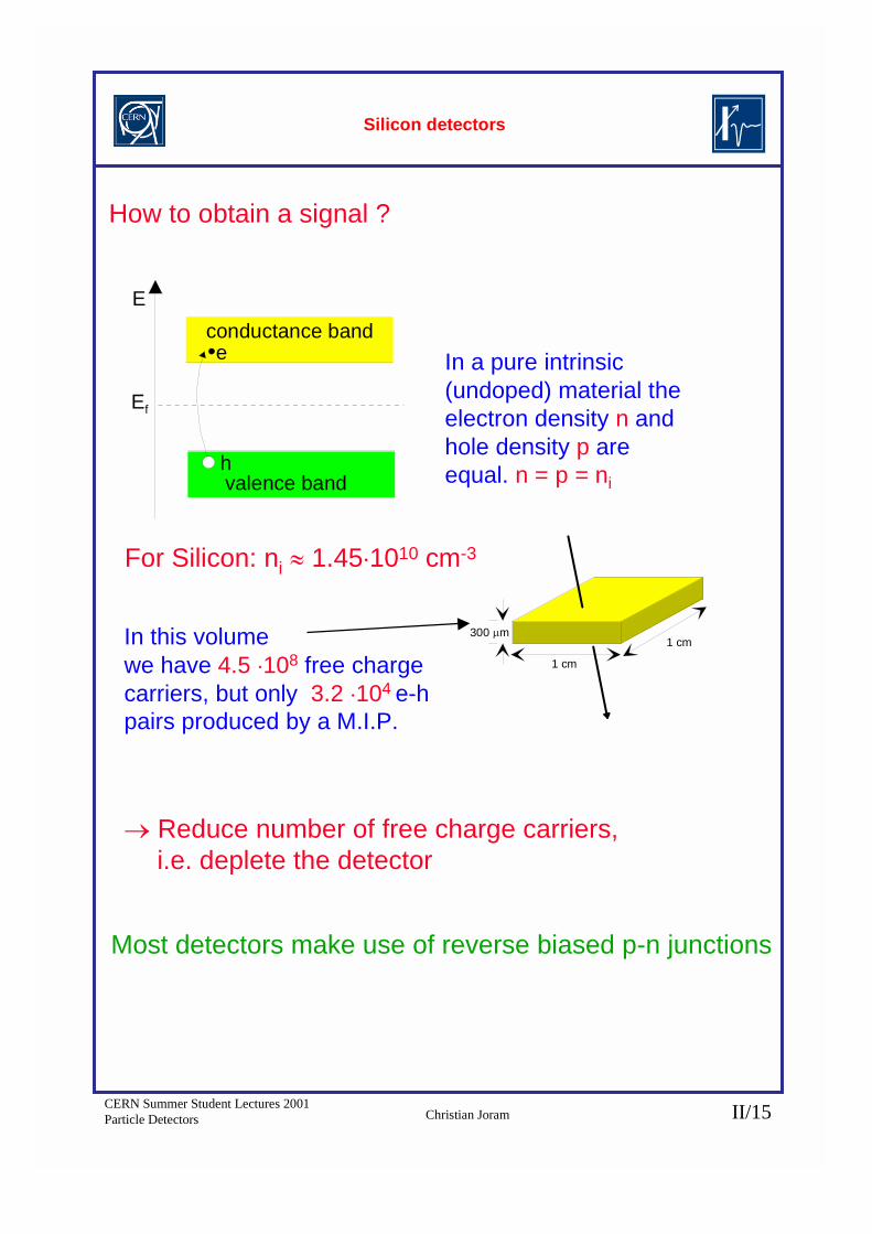
How to obtain a signal ?
Most detectors make use of reverse biased p-n junctions
Ef
E
valence band
conductance band
h
e In a pure intrinsic(undoped) material theelectron density n andhole density p areequal. n = p = ni
For Silicon: ni � 1.45�1010 cm-3
300 �m
1 cm
1 cmIn this volumewe have 4.5 �108 free chargecarriers, but only 3.2 �104 e-hpairs produced by a M.I.P.
� Reduce number of free charge carriers,i.e. deplete the detector
CERN Summer Student Lectures 2001Particle Detectors Christian Joram II/16
Silicon detectors
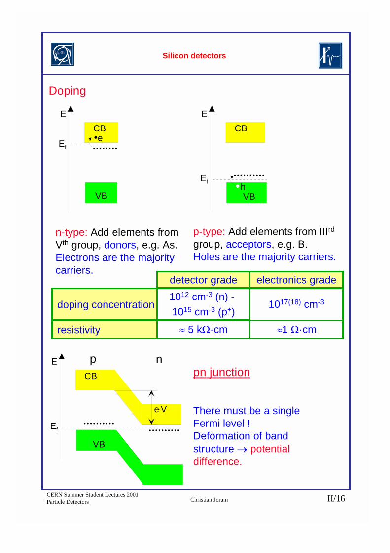
Doping
Ef
E
VB
CBe
n-type: Add elements fromVth group, donors, e.g. As.Electrons are the majoritycarriers.
Ef
E
VB
CB
h
p-type: Add elements from IIIrdgroup, acceptors, e.g. B.Holes are the majority carriers.
doping concentration
Ef
E
VB
CB
p n
e.V
pn junction
There must be a singleFermi level !Deformation of bandstructure � potentialdifference.
detector grade1012 cm-3 (n) - 1015 cm-3 (p+)
electronics grade
1017(18) cm-3
resistivity � 5 k�·cm �1 �·cm
CERN Summer Student Lectures 2001Particle Detectors Christian Joram II/17
Silicon detectors
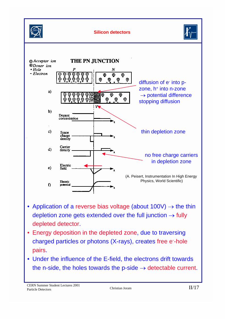
thin depletion zone
no free charge carriersin depletion zone
diffusion of e- into p-zone, h+ into n-zone � potential differencestopping diffusion
• Application of a reverse bias voltage (about 100V) � the thindepletion zone gets extended over the full junction � fullydepleted detector.
• Energy deposition in the depleted zone, due to traversingcharged particles or photons (X-rays), creates free e--holepairs.
• Under the influence of the E-field, the electrons drift towardsthe n-side, the holes towards the p-side � detectable current.
(A. Peisert, Instrumentation In High Energy Physics, World Scientific)
CERN Summer Student Lectures 2001Particle Detectors Christian Joram II/18
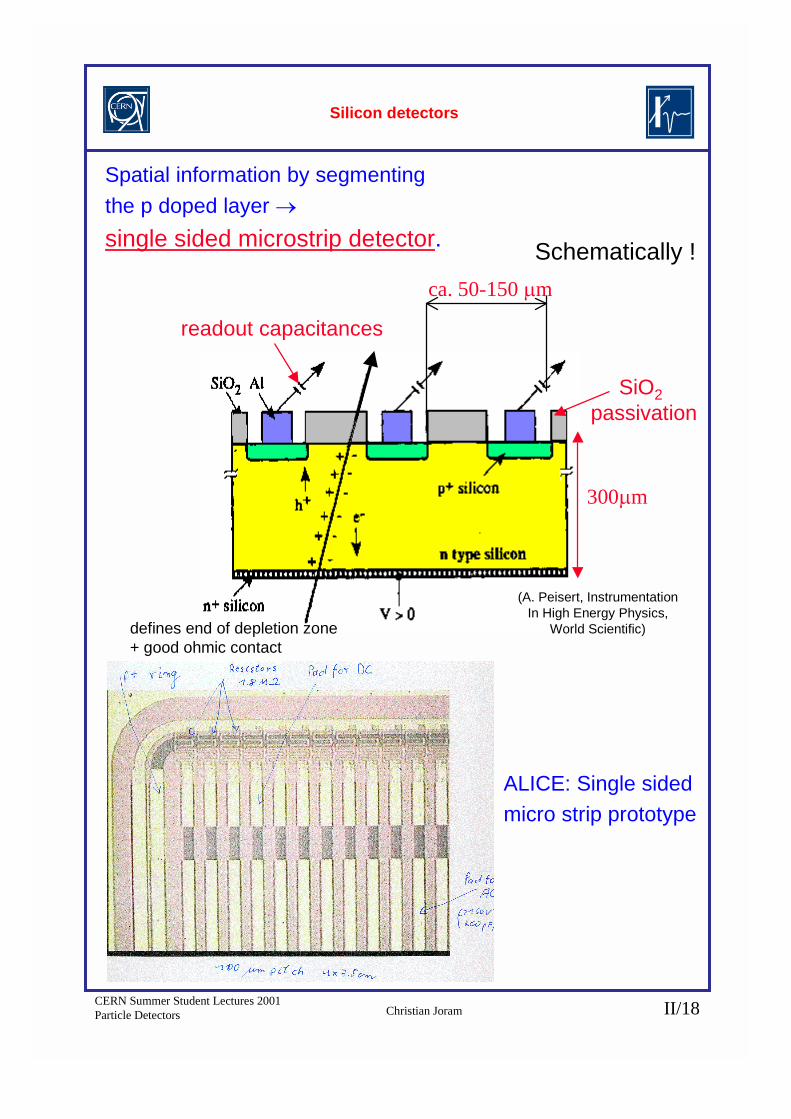
Silicon detectors
Spatial information by segmentingthe p doped layer �single sided microstrip detector.
300�m
SiO2 passivation
readout capacitances
ca. 50-150 �m
Schematically !
(A. Peisert, Instrumentation In High Energy Physics,
World Scientific)defines end of depletion zone + good ohmic contact
ALICE: Single sidedmicro strip prototype
CERN Summer Student Lectures 2001Particle Detectors Christian Joram II/19
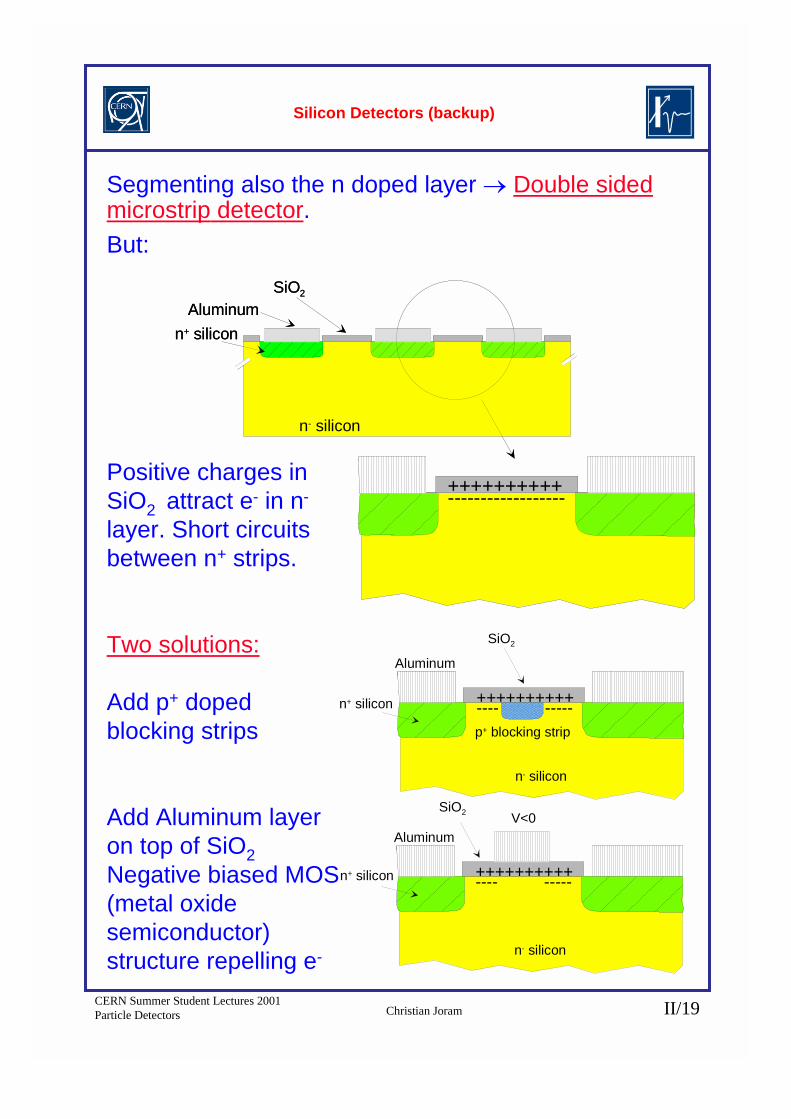
Silicon Detectors (backup)
Segmenting also the n doped layer � Double sidedmicrostrip detector.But:
Alum inumSiO2
n - silicon
n+ silic on
+++ +++++++----- -------------
AluminumSiO2
n- silicon
n+ silicon
++++++++++------------------
AluminumSiO2
n- silicon
n+ silicon
++++++++++------------------Positive charges inSiO2 attract e- in n-
layer. Short circuitsbetween n+ strips.
Two solutions:
Add p+ dopedblocking strips
Add Aluminum layeron top of SiO2Negative biased MOS(metal oxidesemiconductor)structure repelling e-
n- silicon
SiO2
n- silicon
n+ silicon ++++++++++---- -----p+ blocking strip
Aluminum
n- silicon
SiO2
n- silicon
n+ silicon ++++++++++---- -----
AluminumV<0
CERN Summer Student Lectures 2001Particle Detectors Christian Joram II/20
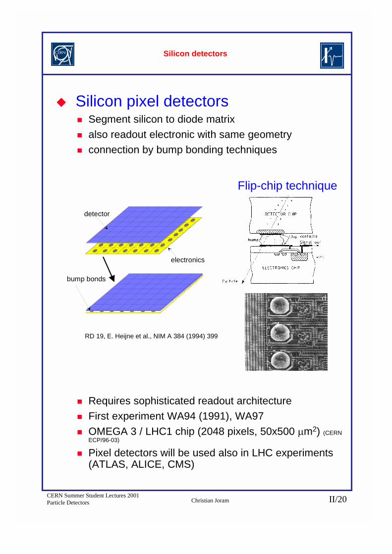
Silicon detectors
� Silicon pixel detectors� Segment silicon to diode matrix� also readout electronic with same geometry� connection by bump bonding techniques
� Requires sophisticated readout architecture� First experiment WA94 (1991), WA97� OMEGA 3 / LHC1 chip (2048 pixels, 50x500 �m2) (CERN
ECP/96-03)
� Pixel detectors will be used also in LHC experiments(ATLAS, ALICE, CMS)
detector
electronics
bump bonds
RD 19, E. Heijne et al., NIM A 384 (1994) 399
Flip-chip technique
CERN Summer Student Lectures 2001Particle Detectors Christian Joram II/21
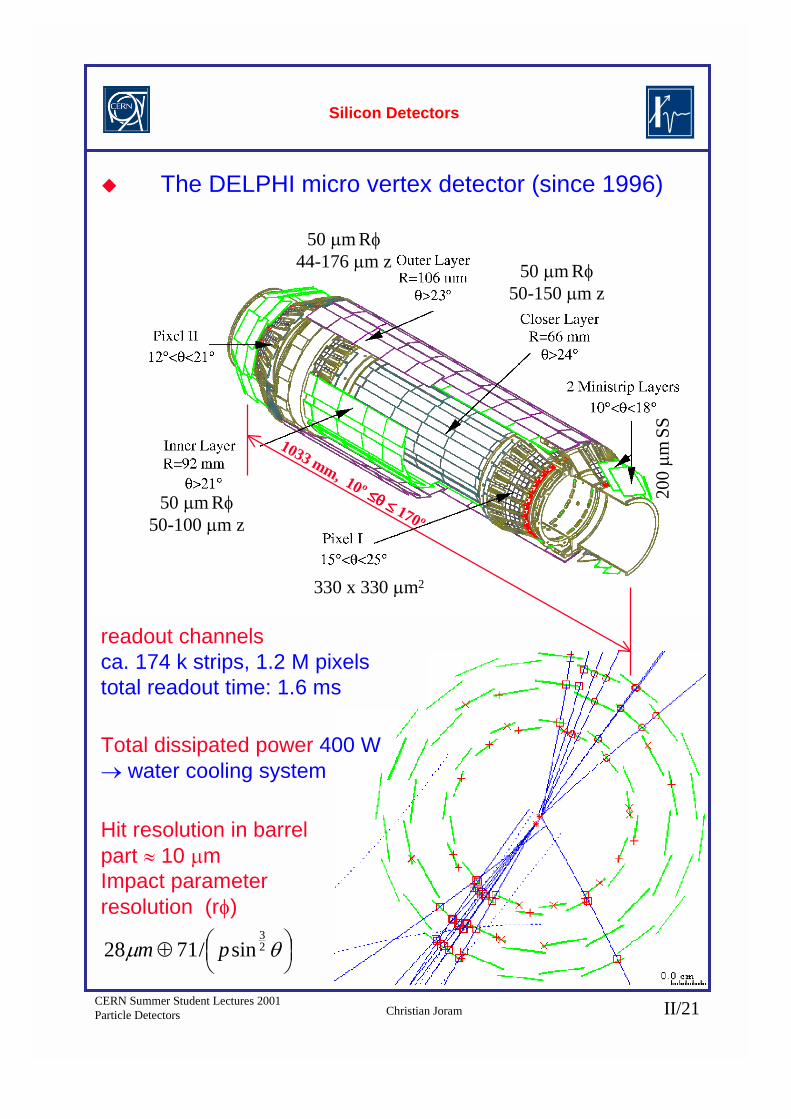
330 x 330 �m2
200 �
m S
S
50 �m R�44-176 �m z
50 �m R�50-100 �m z
50 �m R�50-150 �m z
1033 mm, 10º �������� ���� 170º
Silicon Detectors
� The DELPHI micro vertex detector (since 1996)
Total dissipated power 400 W� water cooling system
Hit resolution in barrelpart � 10 �mImpact parameterresolution (r�)
readout channelsca. 174 k strips, 1.2 M pixelstotal readout time: 1.6 ms
����
��� �� 2
3sin/7128 pm
CERN Summer Student Lectures 2001Particle Detectors Christian Joram II/22
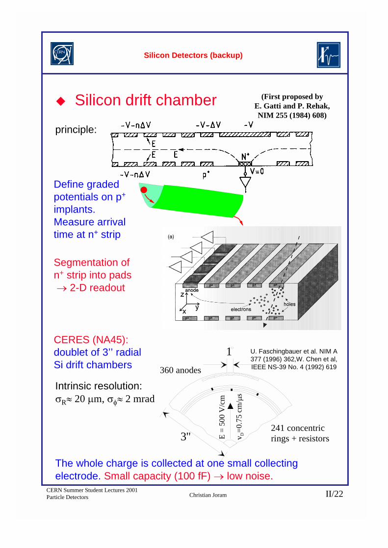
� Silicon drift chamber
Silicon Detectors (backup)
(First proposed byE. Gatti and P. Rehak,NIM 255 (1984) 608)
3''
360 anodes
1
241 concentricrings + resistorsE
= 50
0 V
/cm
v D=0
.75
cm/ �
s
U. Faschingbauer et al. NIM A377 (1996) 362,W. Chen et al,IEEE NS-39 No. 4 (1992) 619
Intrinsic resolution: R� 20 �m, �� 2 mrad
Segmentation of n+ strip into pads � 2-D readout
CERES (NA45): doublet of 3’’ radialSi drift chambers
Define gradedpotentials on p+
implants.Measure arrivaltime at n+ strip
principle:
The whole charge is collected at one small collectingelectrode. Small capacity (100 fF) � low noise.
CERN Summer Student Lectures 2001Particle Detectors Christian Joram II/23
Silicon Detectors (backup)
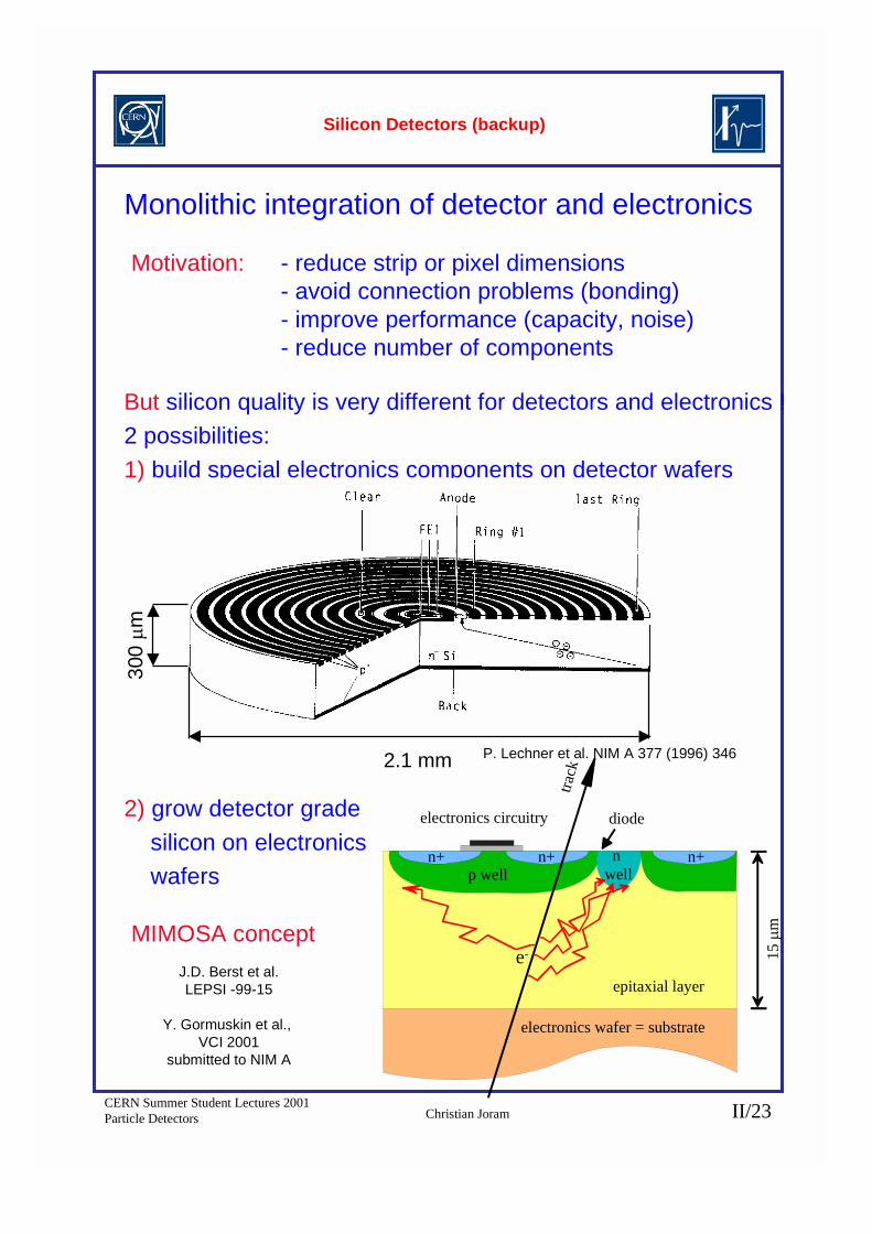
Monolithic integration of detector and electronics
Motivation: - reduce strip or pixel dimensions- avoid connection problems (bonding)- improve performance (capacity, noise)- reduce number of components
But silicon quality is very different for detectors and electronics !2 possibilities:1) build special electronics components on detector wafers
2) grow detector grade silicon on electronics wafers
P. Lechner et al. NIM A 377 (1996) 346
WCC proceedings, page 29top
2.1 mm
300 �
m
electronics wafer = substrate
epitaxial layer
p well n well
diode
e-
electronics circuitry
15 �
m
track
n+ n+ n+
J.D. Berst et al.LEPSI -99-15
Y. Gormuskin et al., VCI 2001
submitted to NIM A
MIMOSA concept
CERN Summer Student Lectures 2001Particle Detectors Christian Joram II/24
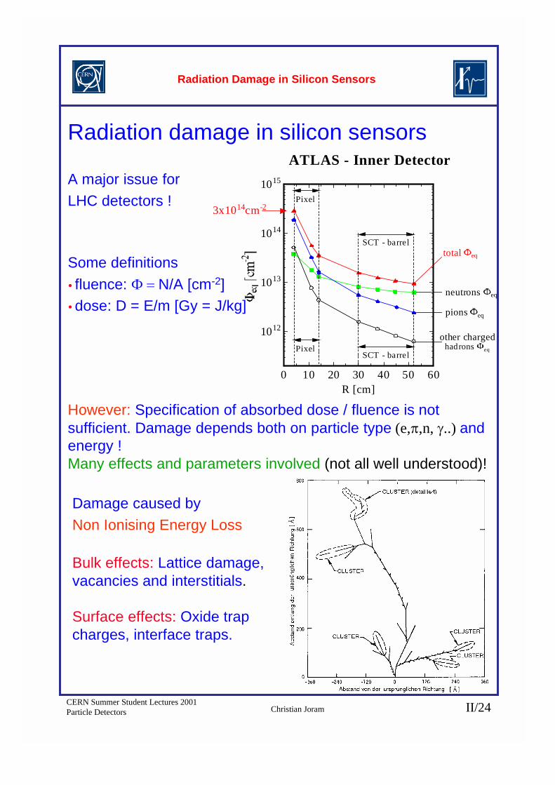
Radiation Damage in Silicon Sensors
Radiation damage in silicon sensors
A major issue forLHC detectors !
0 10 20 30 40 50 60R [cm]
1012
1013
1014
1015
total eq
neutrons eq
pions eq
other chargedhadrons eq
SCT - barrelSCT - barrelPixelPixel
3x1014cm-23x1014cm-2
SCT - barrelSCT - barrel
PixelPixel
ATLAS - Inner Detector
Some definitions� fluence: ���N/A [cm-2]� dose: D = E/m [Gy = J/kg]
However: Specification of absorbed dose / fluence is notsufficient. Damage depends both on particle type (e, ,n, �..) andenergy !Many effects and parameters involved (not all well understood)!
Bulk effects: Lattice damage,vacancies and interstitials.
Surface effects: Oxide trapcharges, interface traps.
Damage caused byNon Ionising Energy Loss
CERN Summer Student Lectures 2001Particle Detectors Christian Joram II/25
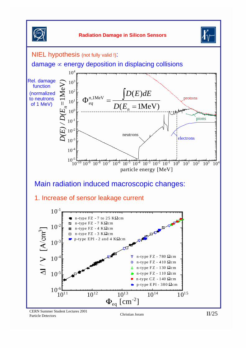
NIEL hypothesis (not fully valid !): damage � energy deposition in displacing collisions
Rel. damagefunction
(normalizedto neutronsof 1 MeV)
10-10 10-9 10-8 10-7 10-6 10-5 10-4 10-3 10-2 10-1 100 101 102 103 104
particle energy [MeV]
10-5
10-4
10-3
10-2
10-1
100
101
102
103
104
neutronsneutrons
pionspions
protonsprotons
electronselectrons
100 101 102 103 104
0.4
0.60.8
1
2
4
neutronsneutrons
pionspions
protonsprotons
)MeV1(
)(MeV1,
���
�n
neq ED
dEED
Main radiation induced macroscopic changes:
1. Increase of sensor leakage current
101 1 1012 101 3 1014 1015
eq [cm-2]10-6
10-5
10-4
10-3
10-2
10-1
n -typ e FZ - 7 to 2 5 K cmn -typ e FZ - 7 to 2 5 K cmn -typ e FZ - 7 K cmn -typ e FZ - 7 K cmn -typ e FZ - 4 K cmn -typ e FZ - 4 K cmn -typ e FZ - 3 K cmn -typ e FZ - 3 K cm
n -type F Z - 7 80 cmn -type F Z - 7 80 cmn -type F Z - 4 10 cmn -type F Z - 4 10 cmn -type F Z - 1 30 cmn -type F Z - 1 30 cmn -type F Z - 1 10 cmn -type F Z - 1 10 cmn -type C Z - 1 40 cmn -type C Z - 1 40 cm
p -ty pe EPI - 2 and 4 K cmp -ty pe EPI - 2 and 4 K cm
p -type E PI - 38 0 cmp -type E PI - 38 0 cm
Radiation Damage in Silicon Sensors
D(E
) / D
(En=
1MeV
)
CERN Summer Student Lectures 2001Particle Detectors Christian Joram II/26
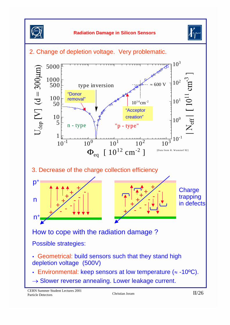
2. Change of depletion voltage. Very problematic.
10-1 100 101 102 103
eq [ 1012 cm-2 ]
1
510
50100
5001000
5000
10-1
100
101
102
103
600 V 600 V
1014cm-21014cm-2
"p - type""p - type"
type inversiontype inversion
n - typen - type
[Data fro m R. W u ns torf 92 ]
How to cope with the radiation damage ?Possible strategies:
� Geometrical: build sensors such that they stand highdepletion voltage (500V)� Environmental: keep sensors at low temperature (� -10ºC).� Slower reverse annealing. Lower leakage current.
“Donorremoval”
“Acceptorcreation”
Radiation Damage in Silicon Sensors
3. Decrease of the charge collection efficiency
+ -
p+
n+
+ --+
-
+ + -
+ -
+ -+ --+
-
+ + -
+ -
Chargetrappingin defectsn
CERN Summer Student Lectures 2001Particle Detectors Christian Joram II/27
Radiation Damage in Silicon Sensors
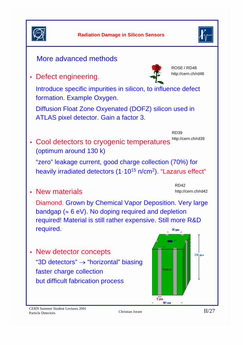
More advanced methods
� Defect engineering.Introduce specific impurities in silicon, to influence defectformation. Example Oxygen.Diffusion Float Zone Oxyenated (DOFZ) silicon used inATLAS pixel detector. Gain a factor 3.
� Cool detectors to cryogenic temperatures(optimum around 130 k)“zero” leakage current, good charge collection (70%) forheavily irradiated detectors (1·1015 n/cm2). “Lazarus effect”
� New materialsDiamond. Grown by Chemical Vapor Deposition. Very largebandgap (� 6 eV). No doping required and depletionrequired! Material is still rather expensive. Still more R&Drequired.
� New detector concepts“3D detectors” � “horizontal” biasingfaster charge collectionbut difficult fabrication process
ROSE / RD48http://cern.ch/rd48
RD39http://cern.ch/rd39
RD42http://cern.ch/rd42