Embed Size (px)
Citation preview
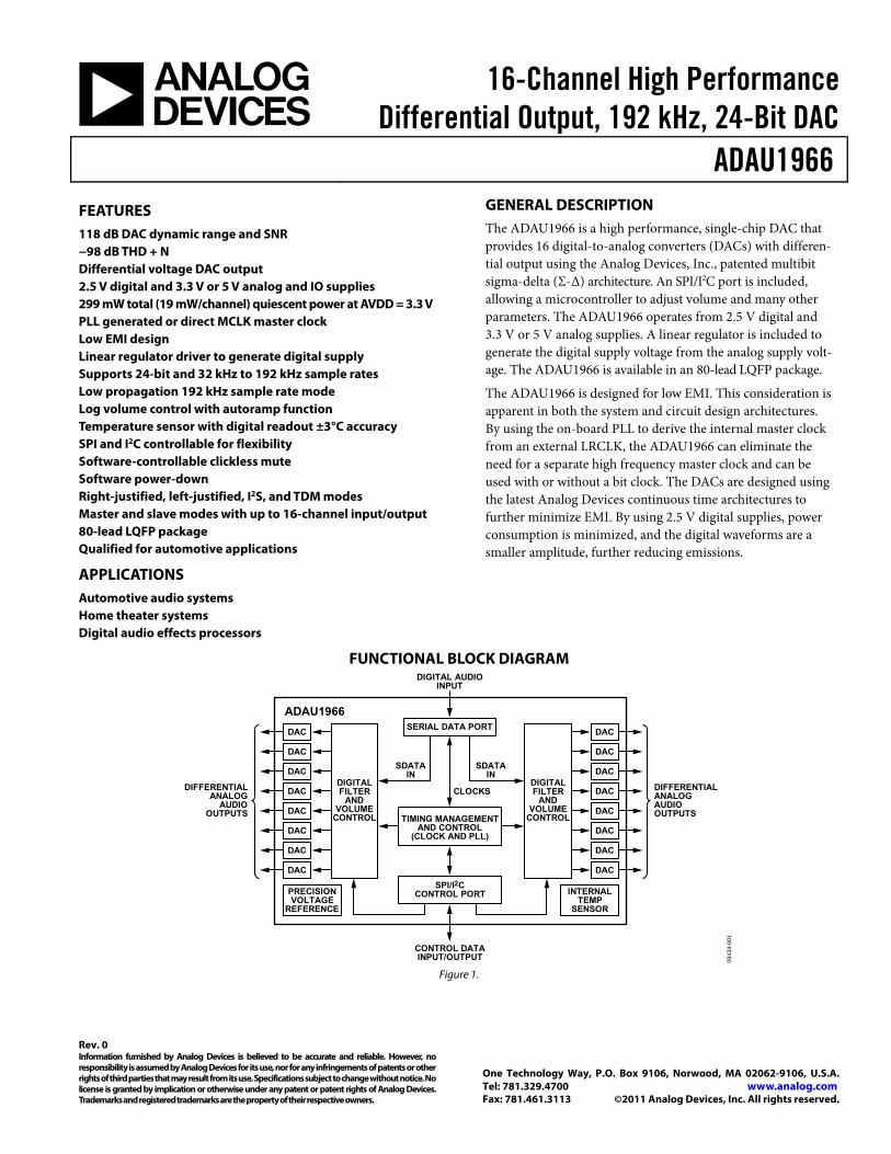
16-Channel High PerformanceDifferential Output, 192 kHz, 24-Bit DAC
ADAU1966
Rev. 0 Information furnished by Analog Devices is believed to be accurate and reliable. However, no responsibility is assumed by Analog Devices for its use, nor for any infringements of patents or other rights of third parties that may result from its use. Specifications subject to change without notice. No license is granted by implication or otherwise under any patent or patent rights of Analog Devices. Trademarks and registered trademarks are the property of their respective owners.
One Technology Way, P.O. Box 9106, Norwood, MA 02062-9106, U.S.A.Tel: 781.329.4700 www.analog.com Fax: 781.461.3113 ©2011 Analog Devices, Inc. All rights reserved.
FEATURES 118 dB DAC dynamic range and SNR −98 dB THD + N Differential voltage DAC output 2.5 V digital and 3.3 V or 5 V analog and IO supplies 299 mW total (19 mW/channel) quiescent power at AVDD = 3.3 V PLL generated or direct MCLK master clock Low EMI design Linear regulator driver to generate digital supply Supports 24-bit and 32 kHz to 192 kHz sample rates Low propagation 192 kHz sample rate mode Log volume control with autoramp function Temperature sensor with digital readout ±3°C accuracy SPI and I2C controllable for flexibility Software-controllable clickless mute Software power-down Right-justified, left-justified, I2S, and TDM modes Master and slave modes with up to 16-channel input/output 80-lead LQFP package Qualified for automotive applications
APPLICATIONS Automotive audio systems Home theater systems Digital audio effects processors
GENERAL DESCRIPTION The ADAU1966 is a high performance, single-chip DAC that provides 16 digital-to-analog converters (DACs) with differen-tial output using the Analog Devices, Inc., patented multibit sigma-delta (Σ-Δ) architecture. An SPI/I2C port is included, allowing a microcontroller to adjust volume and many other parameters. The ADAU1966 operates from 2.5 V digital and 3.3 V or 5 V analog supplies. A linear regulator is included to generate the digital supply voltage from the analog supply volt-age. The ADAU1966 is available in an 80-lead LQFP package.
The ADAU1966 is designed for low EMI. This consideration is apparent in both the system and circuit design architectures. By using the on-board PLL to derive the internal master clock from an external LRCLK, the ADAU1966 can eliminate the need for a separate high frequency master clock and can be used with or without a bit clock. The DACs are designed using the latest Analog Devices continuous time architectures to further minimize EMI. By using 2.5 V digital supplies, power consumption is minimized, and the digital waveforms are a smaller amplitude, further reducing emissions.
FUNCTIONAL BLOCK DIAGRAM
SERIAL DATA PORT
DIGITAL AUDIOINPUT
PRECISIONVOLTAGE
REFERENCE
INTERNALTEMP
SENSOR
TIMING MANAGEMENTAND CONTROL
(CLOCK AND PLL)
SPI/I2CCONTROL PORT
CONTROL DATAINPUT/OUTPUT
ADAU1966
DIFFERENTIALANALOGAUDIOOUTPUTS
DIFFERENTIALANALOG
AUDIOOUTPUTS
DAC
DAC
DAC
DAC
DAC
DAC
DAC
DAC
DAC
DAC
DAC
DAC
DAC
DAC
DAC
DAC
DIGITALFILTER
ANDVOLUME
CONTROL
DIGITALFILTER
ANDVOLUME
CONTROL
SDATAIN
SDATAIN
CLOCKS
0943
4-00
1
Figure 1.
ADAU1966
Rev. 0 | Page 2 of 52
TABLE OF CONTENTS Features .............................................................................................. 1
Applications ....................................................................................... 1
General Description ......................................................................... 1
Functional Block Diagram .............................................................. 1
Revision History ............................................................................... 2
Specifications ..................................................................................... 3
Analog Performance Specifications ........................................... 3
Crystal Oscillator Specifications................................................. 5
Digital Input/Output Specifications........................................... 6
Power Supply Specifications........................................................ 6
Digital Filters ................................................................................. 7
Timing Specifications .................................................................. 7
Absolute Maximum Ratings ............................................................ 9
Thermal Resistance ...................................................................... 9
ESD Caution .................................................................................. 9
Pin Configuration and Function Descriptions ........................... 10
Typical Performance Characteristics ........................................... 13
Application Circuits ....................................................................... 14
Theory of Operation ...................................................................... 15
Digital-to-Analog Converters (DACs) .................................... 15
Clock Signals ............................................................................... 15
Power-Up and RST ..................................................................... 16
Standalone Mode ........................................................................ 17
I2C Control Port .......................................................................... 17
Serial Control Port: SPI Control Mode ................................... 19
Power Supply and Voltage Reference ....................................... 19
Serial Data Ports—Data Format ............................................... 19
Time-Division Multiplexed (TDM) Modes ............................ 19
Temperature Sensor ................................................................... 20
Additional Modes ....................................................................... 22
Register Summary .......................................................................... 23
Register Details ............................................................................... 24
PLL and Clock Control 0 Register ........................................... 24
PLL and Clock Control 1 Register ........................................... 25
Block Power-Down and Thermal Sensor Control 1 Register26
Power-Down Control 2 Register .............................................. 27
Power-Down Control 3 Register .............................................. 28
Thermal Sensor Temperature Readout Register .................... 29
DAC Control 0 Register ............................................................ 30
DAC Control 1 Register ............................................................ 31
DAC Control 2 Register ............................................................ 32
DAC Individual Channel Mutes 1 Register ............................ 33
DAC Individual Channel Mutes 2 Register ............................ 34
Master Volume Control Register .............................................. 35
DAC 1 Volume Control Register .............................................. 35
DAC 2 Volume Control Register .............................................. 36
DAC 3 Volume Control Register .............................................. 36
DAC 4 Volume Control Register .............................................. 37
DAC 5 Volume Control Register .............................................. 37
DAC 6 Volume Control Register .............................................. 38
DAC 7 Volume Control Register .............................................. 38
DAC 8 Volume Control Register .............................................. 39
DAC 9 Volume Control Register .............................................. 39
DAC 10 Volume Control Register ............................................ 40
DAC 11 Volume Control Register ............................................ 40
DAC 12 Volume Control Register ............................................ 41
DAC 13 Volume Control Register ............................................ 41
DAC 14 Volume Control Register ............................................ 42
DAC 15 Volume Control Register ............................................ 42
DAC 16 Volume Control Register ............................................ 43
Common-Mode and Pad Strength Register ........................... 43
DAC Power Adjust 1 Register ................................................... 44
DAC Power Adjust 2 Register ................................................... 45
DAC Power Adjust 3 Register ................................................... 46
DAC Power Adjust 4 Register ................................................... 47
Outline Dimensions ....................................................................... 51
Ordering Guide .......................................................................... 51
Automotive Products ................................................................. 51
REVISION HISTORY 9/11—Revision 0: Initial Version
ADAU1966
Rev. 0 | Page 3 of 52
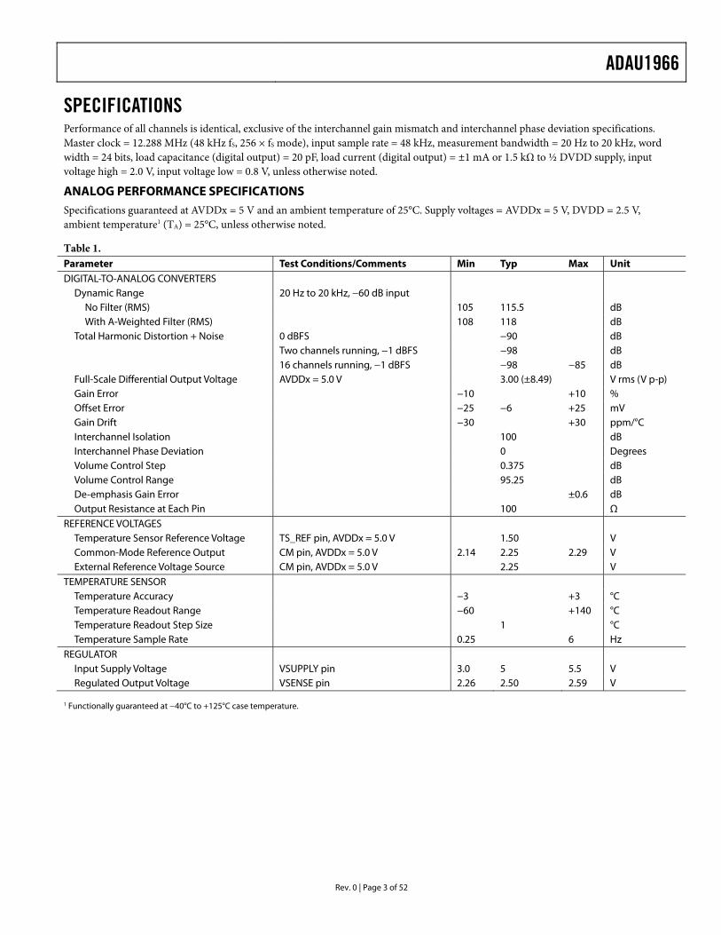
SPECIFICATIONS Performance of all channels is identical, exclusive of the interchannel gain mismatch and interchannel phase deviation specifications. Master clock = 12.288 MHz (48 kHz fS, 256 × fS mode), input sample rate = 48 kHz, measurement bandwidth = 20 Hz to 20 kHz, word width = 24 bits, load capacitance (digital output) = 20 pF, load current (digital output) = ±1 mA or 1.5 kΩ to ½ DVDD supply, input voltage high = 2.0 V, input voltage low = 0.8 V, unless otherwise noted.
ANALOG PERFORMANCE SPECIFICATIONS Specifications guaranteed at AVDDx = 5 V and an ambient temperature of 25°C. Supply voltages = AVDDx = 5 V, DVDD = 2.5 V, ambient temperature1 (TA) = 25°C, unless otherwise noted.
Table 1. Parameter Test Conditions/Comments Min Typ Max Unit DIGITAL-TO-ANALOG CONVERTERS
Dynamic Range 20 Hz to 20 kHz, −60 dB input No Filter (RMS) 105 115.5 dB With A-Weighted Filter (RMS) 108 118 dB
Total Harmonic Distortion + Noise 0 dBFS −90 dB Two channels running, −1 dBFS −98 dB 16 channels running, −1 dBFS −98 −85 dB Full-Scale Differential Output Voltage AVDDx = 5.0 V 3.00 (±8.49) V rms (V p-p) Gain Error −10 +10 % Offset Error −25 −6 +25 mV Gain Drift −30 +30 ppm/°C Interchannel Isolation 100 dB Interchannel Phase Deviation 0 Degrees Volume Control Step 0.375 dB Volume Control Range 95.25 dB De-emphasis Gain Error ±0.6 dB Output Resistance at Each Pin 100 Ω
REFERENCE VOLTAGES Temperature Sensor Reference Voltage TS_REF pin, AVDDx = 5.0 V 1.50 V Common-Mode Reference Output CM pin, AVDDx = 5.0 V 2.14 2.25 2.29 V External Reference Voltage Source CM pin, AVDDx = 5.0 V 2.25 V
TEMPERATURE SENSOR Temperature Accuracy −3 +3 °C Temperature Readout Range −60 +140 °C Temperature Readout Step Size 1 °C Temperature Sample Rate 0.25 6 Hz
REGULATOR Input Supply Voltage VSUPPLY pin 3.0 5 5.5 V Regulated Output Voltage VSENSE pin 2.26 2.50 2.59 V
1 Functionally guaranteed at −40°C to +125°C case temperature.
ADAU1966
Rev. 0 | Page 4 of 52
Specifications guaranteed at AVDDx = 5 V and an ambient temperature of 105°C. Supply voltages = AVDDx = 5 V, DVDD = 2.5 V, ambient temperature1 (TA) = 105°C, unless otherwise noted.
Table 2. Parameter Test Conditions/Comments Min Typ Max Unit DIGITAL-TO-ANALOG CONVERTERS
Dynamic Range 20 Hz to 20 kHz, −60 dB input No Filter (RMS) 109 113.5 dB With A-Weighted Filter (RMS) 110.5 116 dB
Total Harmonic Distortion + Noise 0 dBFS −85 dB Two channels running −92.5 dB Eight channels running −92.5 −85 dB Full-Scale Differential Output Voltage AVDDx = 5.0 V 3.00 (±8.49) V rms (V p-p) Gain Error −10 +10 % Offset Error −25 −6 +25 mV Gain Drift −30 +30 ppm/°C Interchannel Isolation 100 dB Interchannel Phase Deviation 0 Degrees Volume Control Step 0.375 dB Volume Control Range 95.25 dB De-emphasis Gain Error ±0.6 dB Output Resistance at Each Pin 100 Ω
REFERENCE Temperature Sensor Reference Voltage TS_REF pin, AVDDx = 5.0 V 1.50 V Common-Mode Reference Output CM pin, AVDDx = 5.0 V 2.14 2.25 2.29 V External Reference Voltage Source CM pin, AVDDx = 5.0 V 2.25 V
REGULATOR Input Supply Voltage VSUPPLY pin 3.0 5 5.5 V Regulated Output Voltage VSENSE pin 2.25 2.50 2.55 V
1 Functionally guaranteed at −40°C to +125°C case temperature.
Specifications guaranteed at AVDDx = 3.3 V and an ambient temperature of 25°C. Supply voltages = AVDDx = 3.3 V, DVDD = 2.5 V, ambient temperature1 (TA) = 25°C, unless otherwise noted.
Table 3. Parameter Test Conditions/Comments Min Typ Max Unit DIGITAL-TO-ANALOG CONVERTERS
Dynamic Range 20 Hz to 20 kHz, −60 dB input No Filter (RMS) 109 111 dB With A-Weighted Filter (RMS) 111.5 113.5 dB
Total Harmonic Distortion + Noise 0 dBFS −90 dB Two channels running −97 dB Eight channels running −97 −85 dB Full-Scale Differential Output Voltage AVDDx = 3.3 V 2.00 (±5.66) V rms (V p-p) Gain Error −10 +10 % Offset Error −25 −6 +25 mV Gain Drift −30 +30 ppm/°C Interchannel Isolation 100 dB Interchannel Phase Deviation 0 Degrees Volume Control Step 0.375 dB Volume Control Range 95.25 dB De-Emphasis Gain Error ±0.6 dB Output Resistance at Each Pin 100 Ω
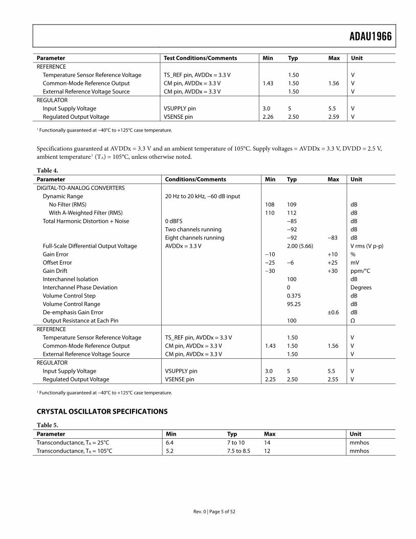
ADAU1966
Rev. 0 | Page 5 of 52
Parameter Test Conditions/Comments Min Typ Max Unit REFERENCE
Temperature Sensor Reference Voltage TS_REF pin, AVDDx = 3.3 V 1.50 V Common-Mode Reference Output CM pin, AVDDx = 3.3 V 1.43 1.50 1.56 V External Reference Voltage Source CM pin, AVDDx = 3.3 V 1.50 V
REGULATOR Input Supply Voltage VSUPPLY pin 3.0 5 5.5 V Regulated Output Voltage VSENSE pin 2.26 2.50 2.59 V
1 Functionally guaranteed at −40°C to +125°C case temperature.
Specifications guaranteed at AVDDx = 3.3 V and an ambient temperature of 105°C. Supply voltages = AVDDx = 3.3 V, DVDD = 2.5 V, ambient temperature1 (TA) = 105°C, unless otherwise noted.
Table 4. Parameter Conditions/Comments Min Typ Max Unit DIGITAL-TO-ANALOG CONVERTERS
Dynamic Range 20 Hz to 20 kHz, −60 dB input No Filter (RMS) 108 109 dB With A-Weighted Filter (RMS) 110 112 dB
Total Harmonic Distortion + Noise 0 dBFS −85 dB Two channels running −92 dB Eight channels running −92 −83 dB Full-Scale Differential Output Voltage AVDDx = 3.3 V 2.00 (5.66) V rms (V p-p) Gain Error −10 +10 % Offset Error −25 −6 +25 mV Gain Drift −30 +30 ppm/°C Interchannel Isolation 100 dB Interchannel Phase Deviation 0 Degrees Volume Control Step 0.375 dB Volume Control Range 95.25 dB De-emphasis Gain Error ±0.6 dB Output Resistance at Each Pin 100 Ω
REFERENCE Temperature Sensor Reference Voltage TS_REF pin, AVDDx = 3.3 V 1.50 V Common-Mode Reference Output CM pin, AVDDx = 3.3 V 1.43 1.50 1.56 V External Reference Voltage Source CM pin, AVDDx = 3.3 V 1.50 V
REGULATOR Input Supply Voltage VSUPPLY pin 3.0 5 5.5 V Regulated Output Voltage VSENSE pin 2.25 2.50 2.55 V
1 Functionally guaranteed at −40°C to +125°C case temperature.
CRYSTAL OSCILLATOR SPECIFICATIONS
Table 5. Parameter Min Typ Max Unit Transconductance, TA = 25°C 6.4 7 to 10 14 mmhos Transconductance, TA = 105°C 5.2 7.5 to 8.5 12 mmhos
ADAU1966
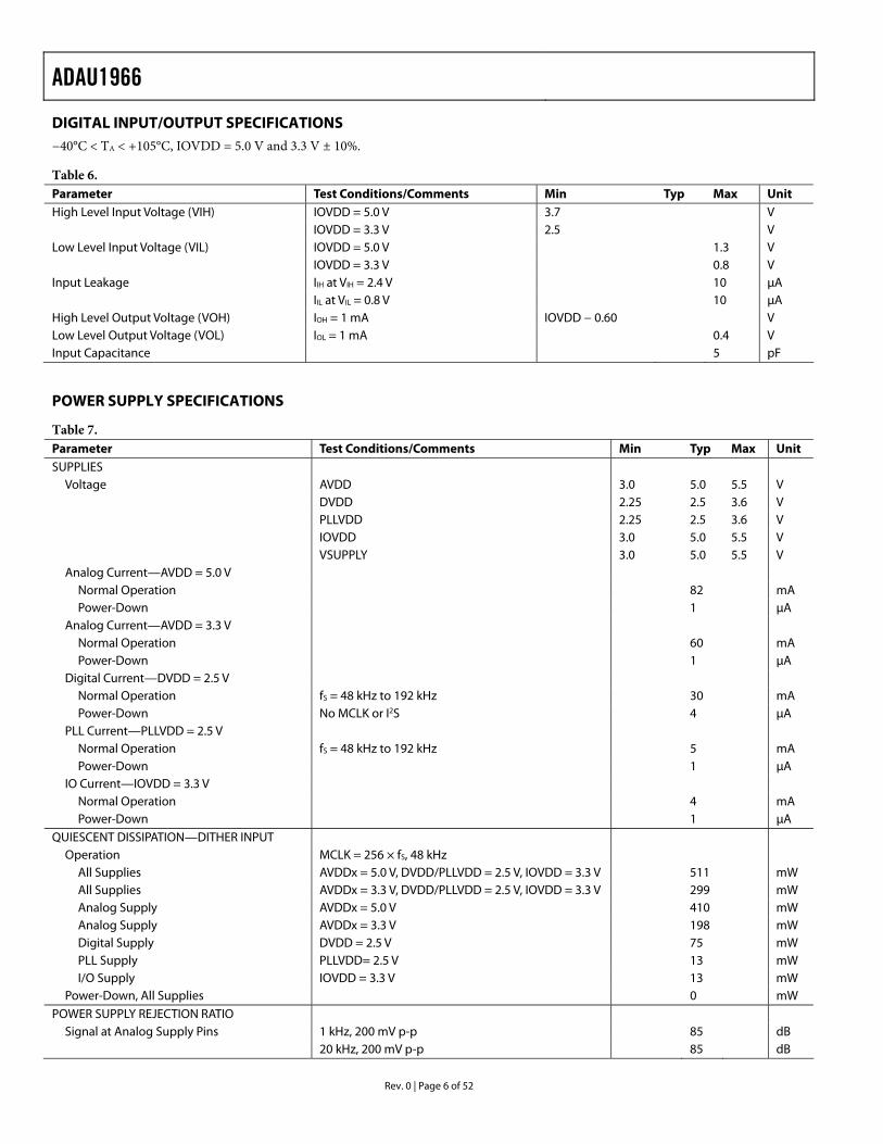
Rev. 0 | Page 6 of 52
DIGITAL INPUT/OUTPUT SPECIFICATIONS −40°C < TA < +105°C, IOVDD = 5.0 V and 3.3 V ± 10%.
Table 6. Parameter Test Conditions/Comments Min Typ Max Unit High Level Input Voltage (VIH) IOVDD = 5.0 V 3.7 V IOVDD = 3.3 V 2.5 V Low Level Input Voltage (VIL) IOVDD = 5.0 V 1.3 V IOVDD = 3.3 V 0.8 V Input Leakage IIH at VIH = 2.4 V 10 μA IIL at VIL = 0.8 V 10 μA High Level Output Voltage (VOH) IOH = 1 mA IOVDD − 0.60 V Low Level Output Voltage (VOL) IOL = 1 mA 0.4 V Input Capacitance 5 pF
POWER SUPPLY SPECIFICATIONS
Table 7. Parameter Test Conditions/Comments Min Typ Max Unit SUPPLIES
Voltage AVDD 3.0 5.0 5.5 V DVDD 2.25 2.5 3.6 V PLLVDD 2.25 2.5 3.6 V IOVDD 3.0 5.0 5.5 V VSUPPLY 3.0 5.0 5.5 V Analog Current—AVDD = 5.0 V
Normal Operation 82 mA Power-Down 1 μA
Analog Current—AVDD = 3.3 V Normal Operation 60 mA Power-Down 1 μA
Digital Current—DVDD = 2.5 V Normal Operation fS = 48 kHz to 192 kHz 30 mA Power-Down No MCLK or I2S 4 μA
PLL Current—PLLVDD = 2.5 V Normal Operation fS = 48 kHz to 192 kHz 5 mA Power-Down 1 μA
IO Current—IOVDD = 3.3 V Normal Operation 4 mA Power-Down 1 μA
QUIESCENT DISSIPATION—DITHER INPUT Operation MCLK = 256 × fS, 48 kHz
All Supplies AVDDx = 5.0 V, DVDD/PLLVDD = 2.5 V, IOVDD = 3.3 V 511 mW All Supplies AVDDx = 3.3 V, DVDD/PLLVDD = 2.5 V, IOVDD = 3.3 V 299 mW Analog Supply AVDDx = 5.0 V 410 mW Analog Supply AVDDx = 3.3 V 198 mW Digital Supply DVDD = 2.5 V 75 mW PLL Supply PLLVDD= 2.5 V 13 mW I/O Supply IOVDD = 3.3 V 13 mW
Power-Down, All Supplies 0 mW POWER SUPPLY REJECTION RATIO
Signal at Analog Supply Pins 1 kHz, 200 mV p-p 85 dB 20 kHz, 200 mV p-p 85 dB
ADAU1966
Rev. 0 | Page 7 of 52
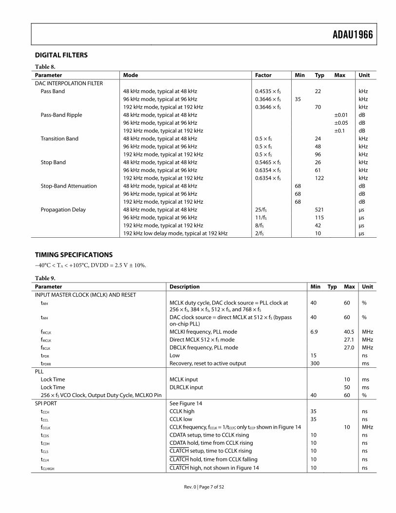
DIGITAL FILTERS
Table 8. Parameter Mode Factor Min Typ Max Unit DAC INTERPOLATION FILTER
Pass Band 48 kHz mode, typical at 48 kHz 0.4535 × fS 22 kHz 96 kHz mode, typical at 96 kHz 0.3646 × fS 35 kHz 192 kHz mode, typical at 192 kHz 0.3646 × fS 70 kHz Pass-Band Ripple 48 kHz mode, typical at 48 kHz ±0.01 dB 96 kHz mode, typical at 96 kHz ±0.05 dB 192 kHz mode, typical at 192 kHz ±0.1 dB Transition Band 48 kHz mode, typical at 48 kHz 0.5 × fS 24 kHz 96 kHz mode, typical at 96 kHz 0.5 × fS 48 kHz 192 kHz mode, typical at 192 kHz 0.5 × fS 96 kHz Stop Band 48 kHz mode, typical at 48 kHz 0.5465 × fS 26 kHz 96 kHz mode, typical at 96 kHz 0.6354 × fS 61 kHz 192 kHz mode, typical at 192 kHz 0.6354 × fS 122 kHz Stop-Band Attenuation 48 kHz mode, typical at 48 kHz 68 dB 96 kHz mode, typical at 96 kHz 68 dB 192 kHz mode, typical at 192 kHz 68 dB Propagation Delay 48 kHz mode, typical at 48 kHz 25/fS 521 μs
96 kHz mode, typical at 96 kHz 11/fS 115 μs 192 kHz mode, typical at 192 kHz 8/fS 42 μs 192 kHz low delay mode, typical at 192 kHz 2/fS 10 μs
TIMING SPECIFICATIONS −40°C < TA < +105°C, DVDD = 2.5 V ± 10%.
Table 9. Parameter Description Min Typ Max Unit INPUT MASTER CLOCK (MCLK) AND RESET
tMH MCLK duty cycle, DAC clock source = PLL clock at 256 × fS, 384 × fS, 512 × fS, and 768 × fS
40 60 %
tMH DAC clock source = direct MCLK at 512 × fS (bypass on-chip PLL)
40 60 %
fMCLK MCLKI frequency, PLL mode 6.9 40.5 MHz fMCLK Direct MCLK 512 × fS mode 27.1 MHz fBCLK DBCLK frequency, PLL mode 27.0 MHz tPDR Low 15 ns tPDRR Recovery, reset to active output 300 ms
PLL Lock Time MCLK input 10 ms Lock Time DLRCLK input 50 ms 256 × fS VCO Clock, Output Duty Cycle, MCLKO Pin 40 60 %
SPI PORT See Figure 14 tCCH CCLK high 35 ns tCCL CCLK low 35 ns fCCLK CCLK frequency, fCCLK = 1/tCCP; only tCCP shown in Figure 14 10 MHz tCDS CDATA setup, time to CCLK rising 10 ns tCDH CDATA hold, time from CCLK rising 10 ns tCLS CLATCH setup, time to CCLK rising 10 ns
tCLH CLATCH hold, time from CCLK falling 10 ns
tCLHIGH CLATCH high, not shown in Figure 14 10 ns
ADAU1966
Rev. 0 | Page 8 of 52
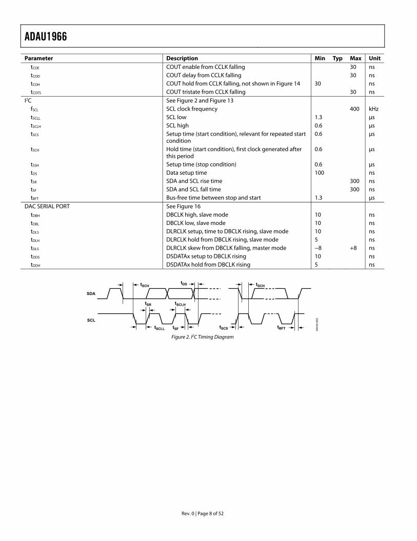
Parameter Description Min Typ Max Unit tCOE COUT enable from CCLK falling 30 ns tCOD COUT delay from CCLK falling 30 ns tCOH COUT hold from CCLK falling, not shown in Figure 14 30 ns tCOTS COUT tristate from CCLK falling 30 ns
I2C See Figure 2 and Figure 13 fSCL SCL clock frequency 400 kHz tSCLL SCL low 1.3 μs tSCLH SCL high 0.6 μs tSCS Setup time (start condition), relevant for repeated start
condition 0.6 μs
tSCH Hold time (start condition), first clock generated after this period
0.6 μs
tSSH Setup time (stop condition) 0.6 μs tDS Data setup time 100 ns tSR SDA and SCL rise time 300 ns tSF SDA and SCL fall time 300 ns tBFT Bus-free time between stop and start 1.3 μs
DAC SERIAL PORT See Figure 16 tDBH DBCLK high, slave mode 10 ns tDBL DBCLK low, slave mode 10 ns tDLS DLRCLK setup, time to DBCLK rising, slave mode 10 ns tDLH DLRCLK hold from DBCLK rising, slave mode 5 ns tDLS DLRCLK skew from DBCLK falling, master mode −8 +8 ns tDDS DSDATAx setup to DBCLK rising 10 ns tDDH DSDATAx hold from DBCLK rising 5 ns
tSCH
tSCLHtSR
tSCLL tSF
tDS
SDA
SCL
tSCH
tBFTtSCS 0943
4-00
2
Figure 2. I2C Timing Diagram
ADAU1966
Rev. 0 | Page 9 of 52
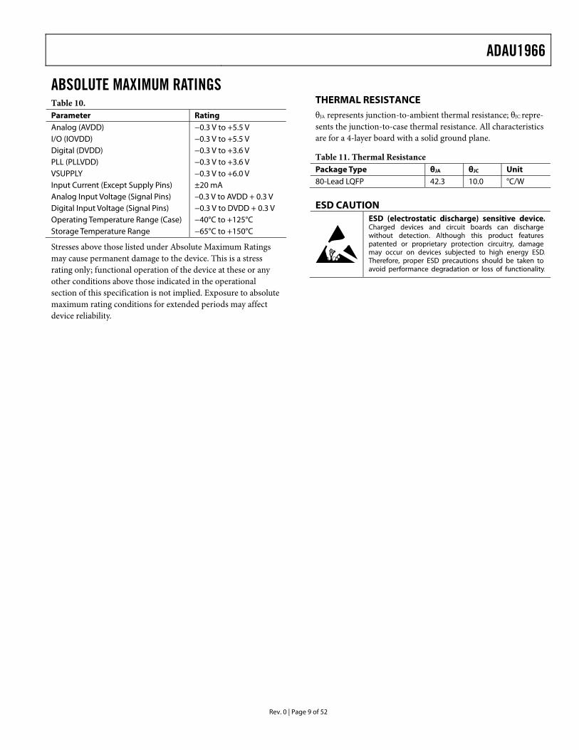
ABSOLUTE MAXIMUM RATINGS Table 10. Parameter Rating Analog (AVDD) −0.3 V to +5.5 V I/O (IOVDD) −0.3 V to +5.5 V Digital (DVDD) −0.3 V to +3.6 V PLL (PLLVDD) −0.3 V to +3.6 V VSUPPLY −0.3 V to +6.0 V Input Current (Except Supply Pins) ±20 mA Analog Input Voltage (Signal Pins) –0.3 V to AVDD + 0.3 V Digital Input Voltage (Signal Pins) −0.3 V to DVDD + 0.3 V Operating Temperature Range (Case) −40°C to +125°C Storage Temperature Range −65°C to +150°C
Stresses above those listed under Absolute Maximum Ratings may cause permanent damage to the device. This is a stress rating only; functional operation of the device at these or any other conditions above those indicated in the operational section of this specification is not implied. Exposure to absolute maximum rating conditions for extended periods may affect device reliability.
THERMAL RESISTANCE θJA represents junction-to-ambient thermal resistance; θJC repre-sents the junction-to-case thermal resistance. All characteristics are for a 4-layer board with a solid ground plane.
Table 11. Thermal Resistance Package Type θJA θJC Unit 80-Lead LQFP 42.3 10.0 °C/W
ESD CAUTION
ADAU1966
Rev. 0 | Page 10 of 52
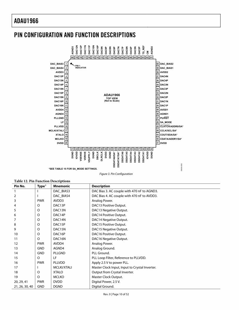
PIN CONFIGURATION AND FUNCTION DESCRIPTIONS
0943
4-00
3
1
2
3
4
5
6
7
8
9
10
11
13
12
14
15
16
17
18
20
19
60
59
58
57
56
55
54
53
52
51
50
49
48
AG
ND
3
DA
C12
N
DA
C12
P
DA
C11
N
DA
C11
P
DA
C10
N
DA
C10
P
DA
C9N
DA
C9P
DA
C8N
DA
C8P
DA
C7N
DA
C7P
PIN 1INDICATOR
47
46
45
44
43
42
41
DAC_BIAS2
DAC_BIAS1
DAC4N
AVDD2
DAC4P
DAC3N
DAC3P
DAC2N
DAC2P
DAC1N
DAC1P
AVDD1
AGND1
PU/RST
SA_MODE
CLATCH/ADDR0/SA*
CCLK/SCL/SA*
COUT/SDA/SA*
CDATA/ADDR1/SA*
DVDD
6162636465666768697071727374757677787980
4039383736353433323130292827262524232221
DG
ND
IOVD
D
VSEN
SE
VDR
IVE
VSU
PPLY
DG
ND
DB
CLK
DLR
CLK
DVD
D
DG
ND
DSD
ATA
8/SA
*
DSD
ATA
7/SA
*
DSD
ATA
6
DSD
ATA
5
DSD
ATA
4
DSD
ATA
3
DSD
ATA
2
DSD
ATA
1
IOVD
D
DG
ND
DA
C6N
DA
C6P
DA
C5N
DA
C5P
TS_R
EF
CM
AG
ND
2
DAC_BIAS3
DAC16P
DAC16N
AVDD4
AGND4
PLLGND
LF
PLLVDD
MCLKI/XTALI
XTALO
MCLKO
DVDD
DAC_BIAS4
AVDD3
DAC13P
DAC13N
DAC14P
DAC14N
DAC15P
DAC15NADAU1966
TOP VIEW(Not to Scale)
*SEE TABLE 15 FOR SA_MODE SETTINGS. Figure 3. Pin Configuration
Table 12. Pin Function Descriptions Pin No. Type1 Mnemonic Description 1 I DAC_BIAS3 DAC Bias 3. AC couple with 470 nF to AGND3. 2 I DAC_BIAS4 DAC Bias 4. AC couple with 470 nF to AVDD3. 3 PWR AVDD3 Analog Power. 4 O DAC13P DAC13 Positive Output. 5 O DAC13N DAC13 Negative Output. 6 O DAC14P DAC14 Positive Output. 7 O DAC14N DAC14 Negative Output. 8 O DAC15P DAC15 Positive Output. 9 O DAC15N DAC15 Negative Output. 10 O DAC16P DAC16 Positive Output. 11 O DAC16N DAC16 Negative Output. 12 PWR AVDD4 Analog Power. 13 GND AGND4 Analog Ground. 14 GND PLLGND PLL Ground. 15 O LF PLL Loop Filter, Reference to PLLVDD. 16 PWR PLLVDD Apply 2.5 V to power PLL. 17 I MCLKI/XTALI Master Clock Input, Input to Crystal Inverter. 18 O XTALO Output from Crystal Inverter. 19 O MCLKO Master Clock Output. 20, 29, 41 PWR DVDD Digital Power, 2.5 V. 21, 26, 30, 40 GND DGND Digital Ground.
ADAU1966
Rev. 0 | Page 11 of 52
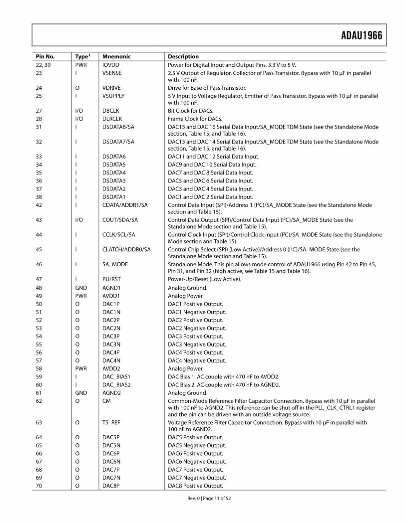
Pin No. Type1 Mnemonic Description 22, 39 PWR IOVDD Power for Digital Input and Output Pins, 3.3 V to 5 V. 23 I VSENSE 2.5 V Output of Regulator, Collector of Pass Transistor. Bypass with 10 μF in parallel
with 100 nF. 24 O VDRIVE Drive for Base of Pass Transistor. 25 I VSUPPLY 5 V Input to Voltage Regulator, Emitter of Pass Transistor. Bypass with 10 μF in parallel
with 100 nF. 27 I/O DBCLK Bit Clock for DACs. 28 I/O DLRCLK Frame Clock for DACs. 31 I DSDATA8/SA DAC15 and DAC 16 Serial Data Input/SA_MODE TDM State (see the Standalone Mode
section, Table 15, and Table 16). 32 I DSDATA7/SA DAC13 and DAC 14 Serial Data Input/SA_MODE TDM State (see the Standalone Mode
section, Table 15, and Table 16). 33 I DSDATA6 DAC11 and DAC 12 Serial Data Input. 34 I DSDATA5 DAC9 and DAC 10 Serial Data Input. 35 I DSDATA4 DAC7 and DAC 8 Serial Data Input. 36 I DSDATA3 DAC5 and DAC 6 Serial Data Input. 37 I DSDATA2 DAC3 and DAC 4 Serial Data Input. 38 I DSDATA1 DAC1 and DAC 2 Serial Data Input. 42 I CDATA/ADDR1/SA Control Data Input (SPI)/Address 1 (I2C)/SA_MODE State (see the Standalone Mode
section and Table 15). 43 I/O COUT/SDA/SA Control Data Output (SPI)/Control Data Input (I2C)/SA_MODE State (see the
Standalone Mode section and Table 15). 44 I CCLK/SCL/SA Control Clock Input (SPI)/Control Clock Input (I2C)/SA_MODE State (see the Standalone
Mode section and Table 15). 45 I CLATCH/ADDR0/SA Control Chip Select (SPI) (Low Active)/Address 0 (I2C)/SA_MODE State (see the
Standalone Mode section and Table 15). 46 I SA_MODE Standalone Mode. This pin allows mode control of ADAU1966 using Pin 42 to Pin 45,
Pin 31, and Pin 32 (high active, see Table 15 and Table 16). 47 I PU/RST Power-Up/Reset (Low Active).
48 GND AGND1 Analog Ground. 49 PWR AVDD1 Analog Power. 50 O DAC1P DAC1 Positive Output. 51 O DAC1N DAC1 Negative Output. 52 O DAC2P DAC2 Positive Output. 53 O DAC2N DAC2 Negative Output. 54 O DAC3P DAC3 Positive Output. 55 O DAC3N DAC3 Negative Output. 56 O DAC4P DAC4 Positive Output. 57 O DAC4N DAC4 Negative Output. 58 PWR AVDD2 Analog Power. 59 I DAC_BIAS1 DAC Bias 1. AC couple with 470 nF to AVDD2. 60 I DAC_BIAS2 DAC Bias 2. AC couple with 470 nF to AGND2. 61 GND AGND2 Analog Ground. 62 O CM Common-Mode Reference Filter Capacitor Connection. Bypass with 10 μF in parallel
with 100 nF to AGND2. This reference can be shut off in the PLL_CLK_CTRL1 register and the pin can be driven with an outside voltage source.
63 O TS_REF Voltage Reference Filter Capacitor Connection. Bypass with 10 μF in parallel with 100 nF to AGND2.
64 O DAC5P DAC5 Positive Output. 65 O DAC5N DAC5 Negative Output. 66 O DAC6P DAC6 Positive Output. 67 O DAC6N DAC6 Negative Output. 68 O DAC7P DAC7 Positive Output. 69 O DAC7N DAC7 Negative Output. 70 O DAC8P DAC8 Positive Output.
ADAU1966
Rev. 0 | Page 12 of 52
Pin No. Type1 Mnemonic Description 71 O DAC8N DAC8 Negative Output. 72 O DAC9P DAC9 Positive Output. 73 O DAC9N DAC9 Negative Output. 74 O DAC10P DAC10 Positive Output. 75 O DAC10N DAC10 Negative Output. 76 O DAC11P DAC11 Positive Output. 77 O DAC11N DAC11 Negative Output. 78 O DAC12P DAC12 Positive Output. 79 O DAC12N DAC12 Negative Output. 80 GND AGND3 Analog Ground. 1 I = input, O = output, I/O = input/output, PWR = power, GND = ground.
ADAU1966
Rev. 0 | Page 13 of 52
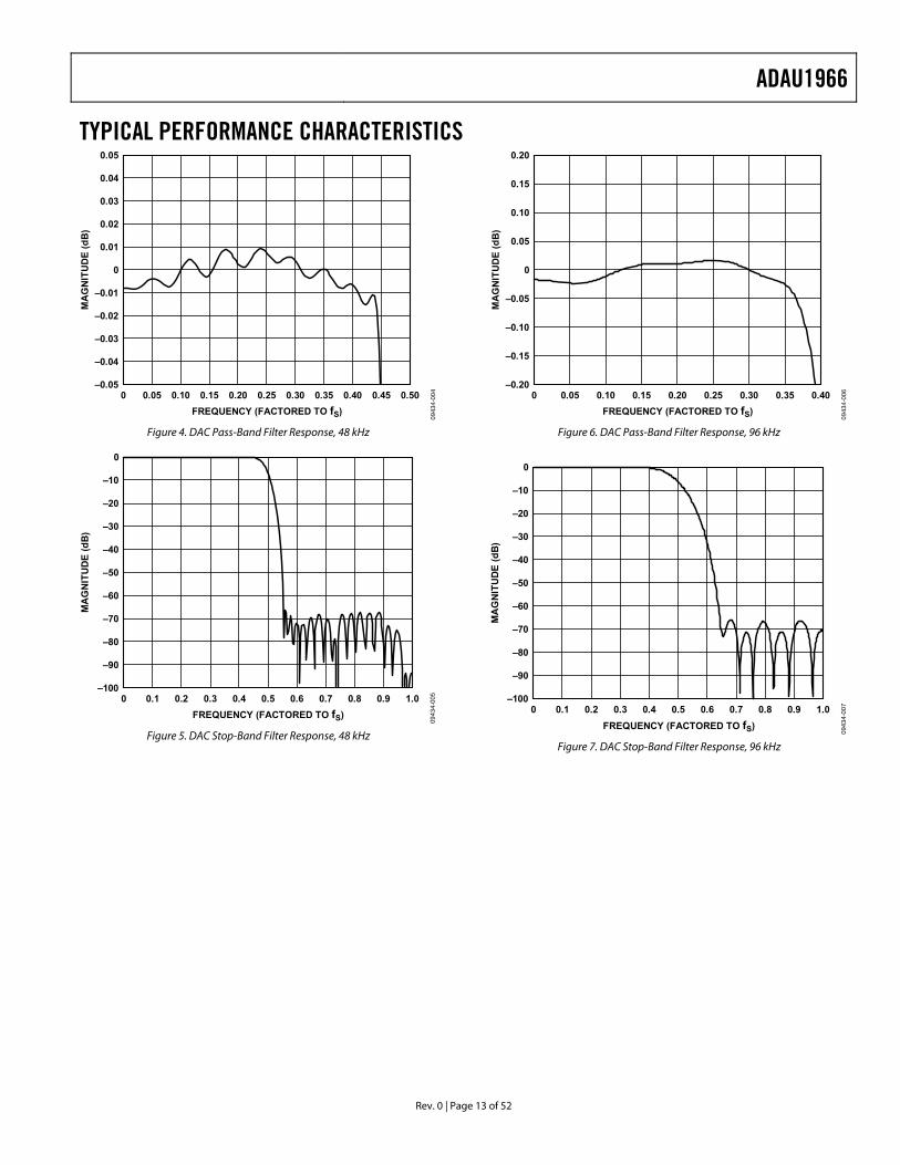
TYPICAL PERFORMANCE CHARACTERISTICS 0.05
–0.05
–0.04
–0.03
–0.02
–0.01
0
0.01
0.02
0.03
0.04
0 0.05 0.10 0.15 0.20 0.25 0.30 0.35 0.40 0.45 0.50
MA
GN
ITU
DE
(dB
)
FREQUENCY (FACTORED TO fS)
0943
4-00
4
Figure 4. DAC Pass-Band Filter Response, 48 kHz
0
–100
–90
–80
–70
–60
–50
–40
–30
–20
–10
0 0.1 0.2 0.3 0.4 0.5 0.6 0.7 0.8 0.9 1.0
MA
GN
ITU
DE
(dB
)
FREQUENCY (FACTORED TO fS)
0943
4-00
5
Figure 5. DAC Stop-Band Filter Response, 48 kHz
0.20
–0.20
–0.15
–0.10
–0.05
0
0.05
0.10
0.15
0 0.05 0.10 0.15 0.20 0.25 0.30 0.35 0.40
MA
GN
ITU
DE
(dB
)
FREQUENCY (FACTORED TO fS)
0943
4-00
6
Figure 6. DAC Pass-Band Filter Response, 96 kHz
0
–100
–90
–80
–70
–60
–50
–40
–30
–20
–10
0 0.1 0.2 0.3 0.4 0.5 0.6 0.7 0.8 0.9 1.0
MA
GN
ITU
DE
(dB
)
FREQUENCY (FACTORED TO fS)
0943
4-00
7
Figure 7. DAC Stop-Band Filter Response, 96 kHz
ADAU1966
Rev. 0 | Page 14 of 52
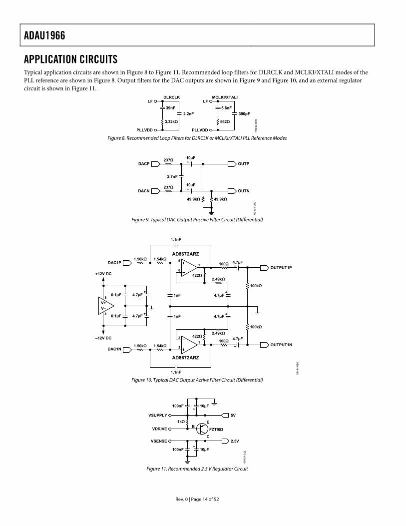
APPLICATION CIRCUITS Typical application circuits are shown in Figure 8 to Figure 11. Recommended loop filters for DLRCLK and MCLKI/XTALI modes of the PLL reference are shown in Figure 8. Output filters for the DAC outputs are shown in Figure 9 and Figure 10, and an external regulator circuit is shown in Figure 11.
39nF2.2nF
LFDLRCLK
PLLVDD
3.32kΩ
5.6nF390pF
LFMCLKI/XTALI
PLLVDD
562Ω
0943
4-00
8
Figure 8. Recommended Loop Filters for DLRCLK or MCLKI/XTALI PLL Reference Modes
2.7nF
DACP OUTP237Ω 10µF
+
DACN OUTN237Ω 10µF
+
49.9kΩ 49.9kΩ
0943
4-00
9
Figure 9. Typical DAC Output Passive Filter Circuit (Differential)
DAC1POUTPUT1P
1.50kΩ 1.54kΩ
422Ω
5
67
AD8672ARZ
1.1nF
4.7µF+100Ω
2.49kΩ
1nF 4.7µF+
DAC1NOUTPUT1N1.50kΩ 1.54kΩ
422Ω
3
21
AD8672ARZ
1.1nF
4.7µF+
100Ω
2.49kΩ
1nF 4.7µF +
100kΩ
100kΩ
4.7µF+
4.7µF +
0.1µF
0.1µF
+12V DC
V+V–
8
4
–12V DC
0943
4-01
0
Figure 10. Typical DAC Output Active Filter Circuit (Differential)
10µF+
E
C
B
VSUPPLY 5V
VSENSE 2.5V
FZT953VDRIVE
1kΩ
100nF
10µF+
100nF
0943
4-01
1
Figure 11. Recommended 2.5 V Regulator Circuit
ADAU1966
Rev. 0 | Page 15 of 52
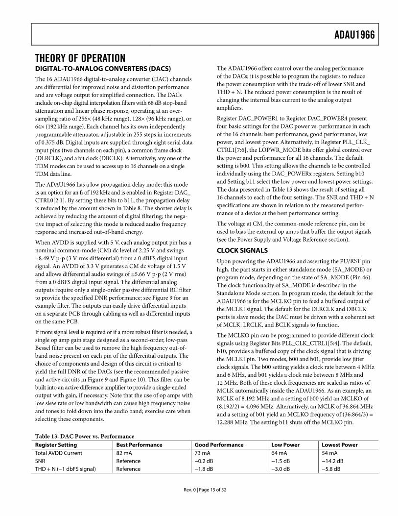
THEORY OF OPERATION DIGITAL-TO-ANALOG CONVERTERS (DACS) The 16 ADAU1966 digital-to-analog converter (DAC) channels are differential for improved noise and distortion performance and are voltage output for simplified connection. The DACs include on-chip digital interpolation filters with 68 dB stop-band attenuation and linear phase response, operating at an over-sampling ratio of 256× (48 kHz range), 128× (96 kHz range), or 64× (192 kHz range). Each channel has its own independently programmable attenuator, adjustable in 255 steps in increments of 0.375 dB. Digital inputs are supplied through eight serial data input pins (two channels on each pin), a common frame clock (DLRCLK), and a bit clock (DBCLK). Alternatively, any one of the TDM modes can be used to access up to 16 channels on a single TDM data line.
The ADAU1966 has a low propagation delay mode; this mode is an option for an fS of 192 kHz and is enabled in Register DAC_ CTRL0[2:1]. By setting these bits to b11, the propagation delay is reduced by the amount shown in Table 8. The shorter delay is achieved by reducing the amount of digital filtering; the nega-tive impact of selecting this mode is reduced audio frequency response and increased out-of-band energy.
When AVDD is supplied with 5 V, each analog output pin has a nominal common-mode (CM) dc level of 2.25 V and swings ±8.49 V p-p (3 V rms differential) from a 0 dBFS digital input signal. An AVDD of 3.3 V generates a CM dc voltage of 1.5 V and allows differential audio swings of ±5.66 V p-p (2 V rms) from a 0 dBFS digital input signal. The differential analog outputs require only a single-order passive differential RC filter to provide the specified DNR performance; see Figure 9 for an example filter. The outputs can easily drive differential inputs on a separate PCB through cabling as well as differential inputs on the same PCB.
If more signal level is required or if a more robust filter is needed, a single op amp gain stage designed as a second-order, low-pass Bessel filter can be used to remove the high frequency out-of-band noise present on each pin of the differential outputs. The choice of components and design of this circuit is critical to yield the full DNR of the DACs (see the recommended passive and active circuits in Figure 9 and Figure 10). This filter can be built into an active difference amplifier to provide a single-ended output with gain, if necessary. Note that the use of op amps with low slew rate or low bandwidth can cause high frequency noise and tones to fold down into the audio band; exercise care when selecting these components.
The ADAU1966 offers control over the analog performance of the DACs; it is possible to program the registers to reduce the power consumption with the trade-off of lower SNR and THD + N. The reduced power consumption is the result of changing the internal bias current to the analog output amplifiers.
Register DAC_POWER1 to Register DAC_POWER4 present four basic settings for the DAC power vs. performance in each of the 16 channels: best performance, good performance, low power, and lowest power. Alternatively, in Register PLL_CLK_ CTRL1[7:6], the LOPWR_MODE bits offer global control over the power and performance for all 16 channels. The default setting is b00. This setting allows the channels to be controlled individually using the DAC_POWERx registers. Setting b10 and Setting b11 select the low power and lowest power settings. The data presented in Table 13 shows the result of setting all 16 channels to each of the four settings. The SNR and THD + N specifications are shown in relation to the measured perfor-mance of a device at the best performance setting.
The voltage at CM, the common-mode reference pin, can be used to bias the external op amps that buffer the output signals (see the Power Supply and Voltage Reference section).
CLOCK SIGNALS
Upon powering the ADAU1966 and asserting the PU/RST pin high, the part starts in either standalone mode (SA_MODE) or program mode, depending on the state of SA_MODE (Pin 46). The clock functionality of SA_MODE is described in the
section. In program mode, the default for the ADAU1966 is for the MCLKO pin to feed a buffered output of the MCLKI signal. The default for the DLRCLK and DBCLK ports is slave mode; the DAC must be driven with a coherent set of MCLK, LRCLK, and BCLK signals to function.
Standalone Mode
The MCLKO pin can be programmed to provide different clock signals using Register Bits PLL_CLK_CTRL1[5:4]. The default, b10, provides a buffered copy of the clock signal that is driving the MCLKI pin. Two modes, b00 and b01, provide low jitter clock signals. The b00 setting yields a clock rate between 4 MHz and 6 MHz, and b01 yields a clock rate between 8 MHz and 12 MHz. Both of these clock frequencies are scaled as ratios of MCLK automatically inside the ADAU1966. As an example, an MCLK of 8.192 MHz and a setting of b00 yield an MCLKO of (8.192/2) = 4.096 MHz. Alternatively, an MCLK of 36.864 MHz and a setting of b01 yield an MCLKO frequency of (36.864/3) = 12.288 MHz. The setting b11 shuts off the MCLKO pin.
Table 13. DAC Power vs. Performance Register Setting Best Performance Good Performance Low Power Lowest Power Total AVDD Current 82 mA 73 mA 64 mA 54 mA SNR Reference −0.2 dB −1.5 dB −14.2 dB THD + N (−1 dbFS signal) Reference −1.8 dB −3.0 dB −5.8 dB
ADAU1966
Rev. 0 | Page 16 of 52
After the PU/RST pin has been asserted high, the PLL_CLK_ CTRLx registers (0x00 and 0x01) can be programmed. The on-chip phase-locked loop (PLL) can be selected to use the clock appearing at the MCLKI/XTALI pin at a frequency of 256, 384, 512, or 768 times the sample rate (fS), referenced to the 48 kHz mode from the master clock select (MCS) setting, as described in . In 96 kHz mode, the master clock fre-quency stays at the same absolute frequency; therefore, the actual multiplication rate is divided by 2. In 192 kHz mode, the actual multiplication rate is divided by 4. For example, if the ADAU1966 is programmed in 256 × fS mode, the frequency of the master clock input is 256 × 48 kHz = 12.288 MHz. If the ADAU1966 is then switched to 96 kHz operation (by writing to DAC_CTRL0 [2:1]), the frequency of the master clock should remain at 12.288 MHz, which is 128 × fS in this example. In 192 kHz mode, MCS becomes 64 × fS.
Table 14
The internal clock for the digital core varies by mode: 512 × fS (48 kHz mode), 256 × fS (96 kHz mode), or 128 × fS (192 kHz mode). By default, the on-board PLL generates this internal master clock from an external clock.
The PLL should be powered and stable before the ADAU1966 is used as a source for quality audio. The PLL is enabled by reset and does not require writing to the I2C or SPI port for normal operation.
With the PLL enabled, the performance of the ADAU1966 is not affected by jitter as high as a 300 ps rms time interval error (TIE). If the internal PLL is not used, it is best to use an independ-ent crystal oscillator to generate the master clock.
If the ADAU1966 is to be used in direct MCLK mode, the PLL can be powered down in the PDN_THRMSENS_CTRL_1 regis-ter. For direct MCLK mode, a 512 × fS (referenced to 48 kHz mode) master clock must be used as MCLK, and the CLK_SEL bit in the PLL_CLK_CTRL1 register must be set to b1.
The ADAU1966 PLL can also be programmed to run from an external LRCLK. When the PLLIN bits in the PLL_CLK_CTRL0 register are set to 01 and the appropriate loop filter is connected to the LF pin (see Figure 8), the ADAU1966 PLL generates all of the necessary internal clocks for operation with no external MCLK. This mode reduces the number of high frequency signals in the design, reducing EMI emissions.
It is possible to further reduce EMI emissions of the circuit by using the internal DBCLK generation setting of the BCLK_GEN
bit in the DAC_CTRL1 register. With the BCLK_GEN bit set to b1 (internal) and the SAI_MS bit set to b0 (slave), the ADAU1966 generate its own DBCLK; this works with the PLL input set to either MCLKI/XTALI or DLRCLK. DLRCLK is the only required clock in DLRCLK PLL mode.
POWER-UP AND RST
Power sequencing for the ADAU1966 should start with AVDD and IOVDD, followed by DVDD. It is very important that AVDD be settled at a regulated voltage and that IOVDD be within 10% of regulated voltage before applying DVDD. When using the ADAU1966 internal regulator, this timing occurs by default.
To guarantee proper startup, the PU/RST pin should be pulled low by an external resistor and then driven high after the power supplies have stabilized. The PU/RST can also be pulled high using a simple RC network.
Driving the PU/RST pin low puts the part into a very low power state (<3 μA). All functionality of the ADAU1966 is disabled until the PU/RST pin is asserted high. Once this pin is asserted high, the ADAU1966 requires 300 ms to stabilize. The MMUTE bit in the DAC_CTRL0 register must be toggled for operation.
The PUP bit in the PLL_CLK_CTRL0 register can be used to power down the ADAU1966. Engaging the master power-down puts the ADAU1966 in an idle state while maintaining the set-tings of all registers. Additionally, the power-down bits in the PDN_THRMSENS_CTRL1 register (TS_PDN, PLL_PDN, and VREG_PDN) can be used to power down individual sections of the ADAU1966.
The SOFT_RST bit in the PLL_CLK_CTRL0 register sets all of the control registers to their default settings while maintaining the internal clocks in default mode. The SOFT_RST bit does not power down the analog outputs; toggling this bit does not cause audible popping sounds at the differential analog outputs.
Proper startup of the ADAU1966 should proceed as follows:
1. Apply power to the ADAU1966 as described previously. 2. Assert the PU/RST pin high after power supplies have
stabilized. 3. Set the PUP bit to b1. 4. Program all necessary registers for the desired settings. 5. Set the MMUTE bit to b0 to unmute all channels.
ADAU1966
Rev. 0 | Page 17 of 52
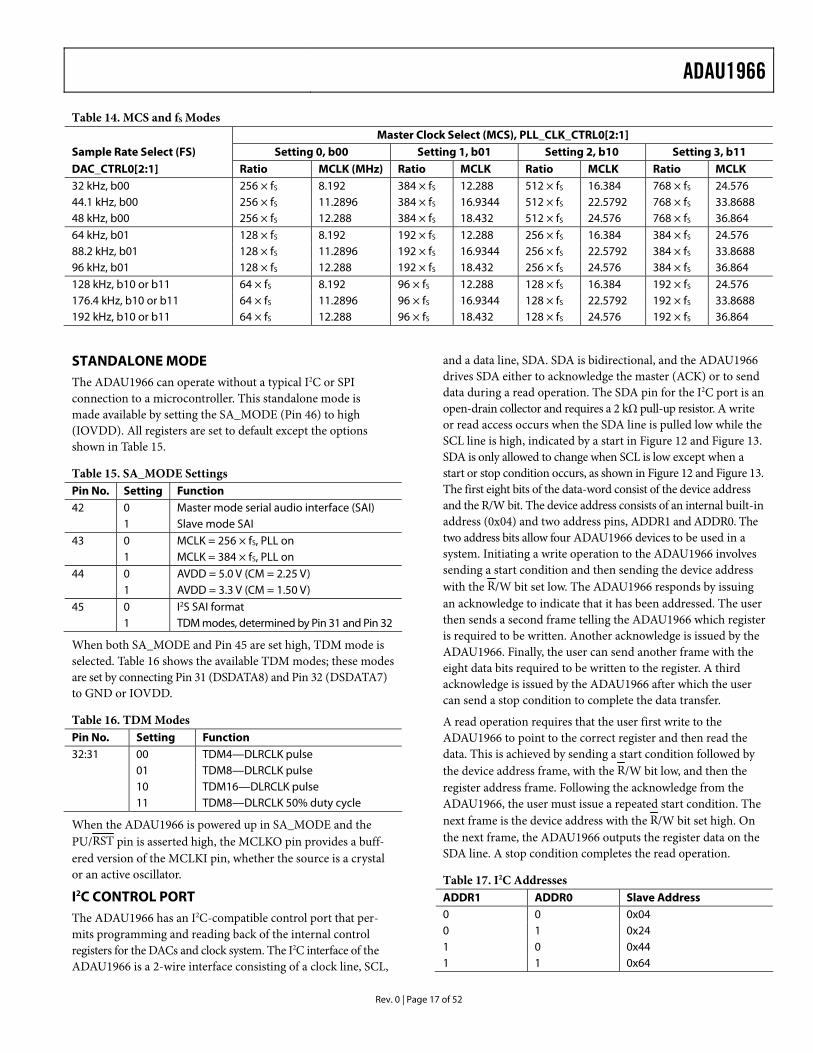
Table 14. MCS and fS Modes Master Clock Select (MCS), PLL_CLK_CTRL0[2:1] Sample Rate Select (FS) Setting 0, b00 Setting 1, b01 Setting 2, b10 Setting 3, b11 DAC_CTRL0[2:1] Ratio MCLK (MHz) Ratio MCLK Ratio MCLK Ratio MCLK 32 kHz, b00 256 × fS 8.192 384 × fS 12.288 512 × fS 16.384 768 × fS 24.576 44.1 kHz, b00 256 × fS 11.2896 384 × fS 16.9344 512 × fS 22.5792 768 × fS 33.8688 48 kHz, b00 256 × fS 12.288 384 × fS 18.432 512 × fS 24.576 768 × fS 36.864 64 kHz, b01 128 × fS 8.192 192 × fS 12.288 256 × fS 16.384 384 × fS 24.576 88.2 kHz, b01 128 × fS 11.2896 192 × fS 16.9344 256 × fS 22.5792 384 × fS 33.8688 96 kHz, b01 128 × fS 12.288 192 × fS 18.432 256 × fS 24.576 384 × fS 36.864 128 kHz, b10 or b11 64 × fS 8.192 96 × fS 12.288 128 × fS 16.384 192 × fS 24.576 176.4 kHz, b10 or b11 64 × fS 11.2896 96 × fS 16.9344 128 × fS 22.5792 192 × fS 33.8688 192 kHz, b10 or b11 64 × fS 12.288 96 × fS 18.432 128 × fS 24.576 192 × fS 36.864
STANDALONE MODE The ADAU1966 can operate without a typical I2C or SPI connection to a microcontroller. This standalone mode is made available by setting the SA_MODE (Pin 46) to high (IOVDD). All registers are set to default except the options shown in Table 15.
Table 15. SA_MODE Settings Pin No. Setting Function 42 0 Master mode serial audio interface (SAI) 1 Slave mode SAI 43 0 MCLK = 256 × fS, PLL on 1 MCLK = 384 × fS, PLL on 44 0 AVDD = 5.0 V (CM = 2.25 V) 1 AVDD = 3.3 V (CM = 1.50 V) 45 0 I2S SAI format 1 TDM modes, determined by Pin 31 and Pin 32
When both SA_MODE and Pin 45 are set high, TDM mode is selected. Table 16 shows the available TDM modes; these modes are set by connecting Pin 31 (DSDATA8) and Pin 32 (DSDATA7) to GND or IOVDD.
Table 16. TDM Modes Pin No. Setting Function 32:31 00 TDM4—DLRCLK pulse 01 TDM8—DLRCLK pulse 10 TDM16—DLRCLK pulse 11 TDM8—DLRCLK 50% duty cycle
When the ADAU1966 is powered up in SA_MODE and the PU/RST pin is asserted high, the MCLKO pin provides a buff-ered version of the MCLKI pin, whether the source is a crystal or an active oscillator.
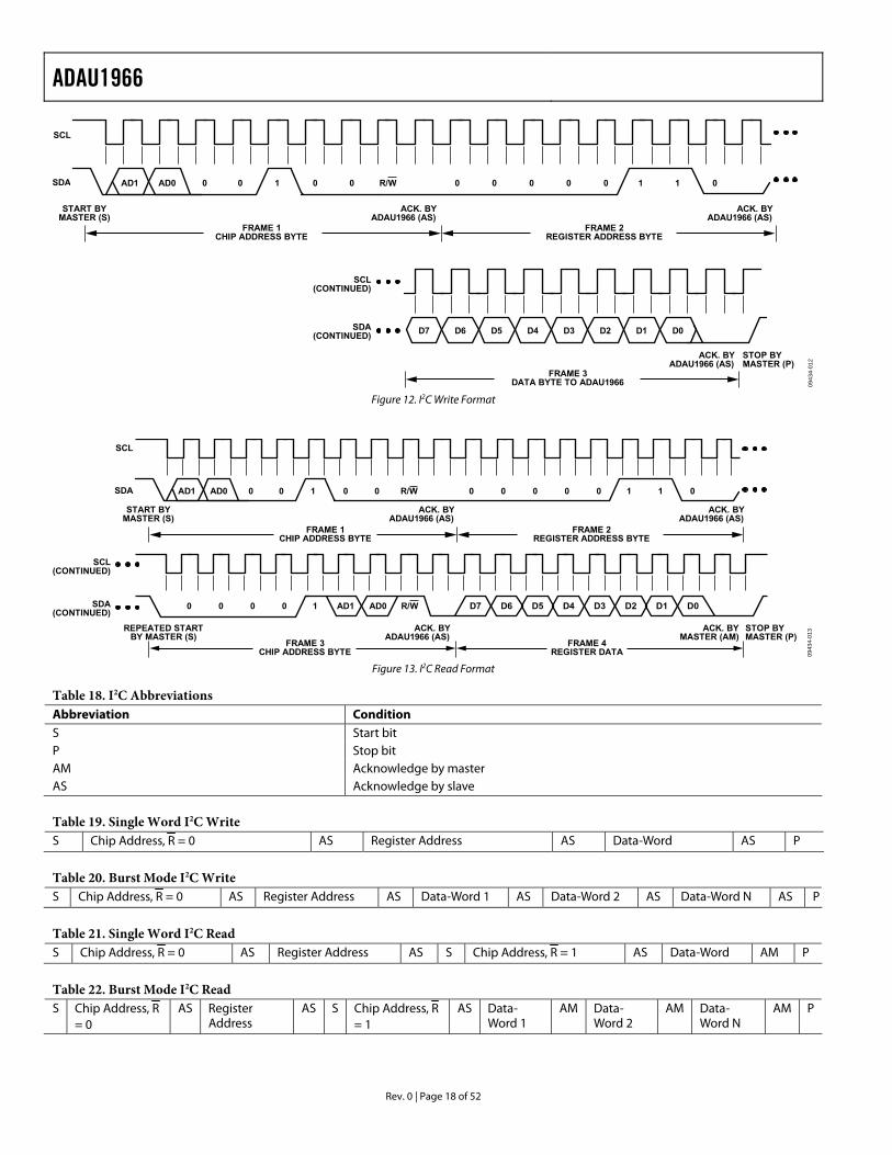
I2C CONTROL PORT The ADAU1966 has an I2C-compatible control port that per-mits programming and reading back of the internal control registers for the DACs and clock system. The I2C interface of the ADAU1966 is a 2-wire interface consisting of a clock line, SCL,
and a data line, SDA. SDA is bidirectional, and the ADAU1966 drives SDA either to acknowledge the master (ACK) or to send data during a read operation. The SDA pin for the I2C port is an open-drain collector and requires a 2 kΩ pull-up resistor. A write or read access occurs when the SDA line is pulled low while the SCL line is high, indicated by a start in Figure 12 and Figure 13. SDA is only allowed to change when SCL is low except when a start or stop condition occurs, as shown in Figure 12 and Figure 13. The first eight bits of the data-word consist of the device address and the R/W bit. The device address consists of an internal built-in address (0x04) and two address pins, ADDR1 and ADDR0. The two address bits allow four ADAU1966 devices to be used in a system. Initiating a write operation to the ADAU1966 involves sending a start condition and then sending the device address with the R/W bit set low. The ADAU1966 responds by issuing an acknowledge to indicate that it has been addressed. The user then sends a second frame telling the ADAU1966 which register is required to be written. Another acknowledge is issued by the ADAU1966. Finally, the user can send another frame with the eight data bits required to be written to the register. A third acknowledge is issued by the ADAU1966 after which the user can send a stop condition to complete the data transfer.
A read operation requires that the user first write to the ADAU1966 to point to the correct register and then read the data. This is achieved by sending a start condition followed by the device address frame, with the R/W bit low, and then the register address frame. Following the acknowledge from the ADAU1966, the user must issue a repeated start condition. The next frame is the device address with the R/W bit set high. On the next frame, the ADAU1966 outputs the register data on the SDA line. A stop condition completes the read operation.
Table 17. I2C Addresses ADDR1 ADDR0 Slave Address 0 0 0x04 0 1 0x24 1 0 0x44 1 1 0x64
ADAU1966
Rev. 0 | Page 18 of 52
AD0AD1 0 0 1 0 0 R/W 0 0 0 0 0 011
SCL
SDA
SCL(CONTINUED)
SDA(CONTINUED)
START BYMASTER (S)
ACK. BYADAU1966 (AS)
ACK. BYADAU1966 (AS)
ACK. BYADAU1966 (AS)
STOP BYMASTER (P)
FRAME 1CHIP ADDRESS BYTE
FRAME 2REGISTER ADDRESS BYTE
FRAME 3DATA BYTE TO ADAU1966
D7 D6 D5 D4 D3 D2 D1 D0
0943
4-01
2
Figure 12. I2C Write Format
SCL
FRAME 4REGISTER DATA
FRAME 3CHIP ADDRESS BYTE
ACK. BYMASTER (AM)
ACK. BYADAU1966 (AS)
REPEATED STARTBY MASTER (S)
STOP BYMASTER (P)
SCL(CONTINUED)
SDA(CONTINUED)
START BYMASTER (S)
ACK. BYADAU1966 (AS)
ACK. BYADAU1966 (AS)
FRAME 1CHIP ADDRESS BYTE
FRAME 2REGISTER ADDRESS BYTE
AD0AD1 0 0 1 0 0 R/W 0 0 0 0 0 011SDA
D7AD010000 AD1 D6 D5 D4 D3 D2 D1 D0R/W
0943
4-01
3
Figure 13. I2C Read Format
Table 18. I2C Abbreviations Abbreviation Condition S Start bit P Stop bit AM Acknowledge by master AS Acknowledge by slave
Table 19. Single Word I2C Write S Chip Address, R = 0 AS Register Address AS Data-Word AS P
Table 20. Burst Mode I2C Write S Chip Address, R = 0 AS Register Address AS Data-Word 1 AS Data-Word 2 AS Data-Word N AS P
Table 21. Single Word I2C Read S Chip Address, R = 0 AS Register Address AS S Chip Address, R = 1 AS Data-Word AM P
Table 22. Burst Mode I2C Read S Chip Address, R
= 0 AS Register
Address AS S Chip Address, R
= 1 AS Data-
Word 1 AM Data-
Word 2 AM Data-
Word N AM P
ADAU1966
Rev. 0 | Page 19 of 52
SERIAL CONTROL PORT: SPI CONTROL MODE The ADAU1966 has an SPI control port that permits program-ming and reading back of the internal control registers for the DACs and clock system. A standalone mode is also available for operation without serial control; it is configured at reset using the SA_MODE pin. See the Standalone Mode section for details about SA_MODE.
By default, the ADAU1966 is in I2C mode, but it can be put into SPI control mode by pulling CLATCH low three times. This is done by performing three dummy writes to the SPI port (the ADAU1966 does not acknowledge these three writes). Begin-ning with the fourth SPI write, data can be written to or read from the IC. The ADAU1966 can be taken out of SPI control mode only by a full reset initiated by power cycling the IC.
The SPI control port of the ADAU1966 is a 4-wire serial control port. The format is similar to the Motorola SPI format except the input data-word is 24 bits wide. The serial bit clock and latch can be completely asynchronous to the sample rate of the DACs. Figure 14 shows the format of the SPI signal. The first byte is a global address with a read/write bit. For the ADAU1966, the address is 0x06, shifted left one bit due to the R/W bit. The second byte is the ADAU1966 register address, and the third byte is the data.
POWER SUPPLY AND VOLTAGE REFERENCE The ADAU1966 is designed for 3.3 V or 5 V analog and 2.5 V digital supplies. To minimize noise pickup, the power supply pins should be bypassed with 100 nF ceramic chip capacitors placed as close to the pins as possible. A bulk aluminum electrolytic capacitor of at least 22 μF should also be provided for each rail on the same PC board as the codec. It is important that the analog supply be as clean as possible.
The ADAU1966 includes a 2.5 V regulator driver that requires only an external pass transistor and bypass capacitors to make a 2.5 V regulator from a 5 V or 3.3 V supply. The VSUPPLY and VSENSE pins should be decoupled with no more than 10 μF, in parallel with 100 nF high frequency bypassing. If the regulator driver is not used, connect VSUPPLY and VDRIVE to GND and leave VSENSE unconnected.
All digital inputs are compatible with TTL and CMOS levels. All outputs are driven from the 3.3 V or 5 V IOVDD supply and are compatible with TTL and 3.3 V CMOS levels.
The temperature sensor internal voltage reference (VTS_REF) is brought out on the TS_REF pin and should be bypassed as close as possible to the chip with a parallel combination of 10 μF and 100 nF.
The internal band gap reference can be disabled in the PLL_CLK_CTRL1 register by setting VREF_EN to 0; the CM pin can be then be driven from an external source. This can be used to scale the DAC output to the clipping level of a power amplifier based on its power supply voltage.
The CM pin is the internal common-mode reference. It should be bypassed as close as possible to the chip, with a parallel combination of 10 μF and 100 nF. This voltage can be used to bias external op amps to the common-mode voltage of the analog input and output signal pins. The output current should be limited to less than 0.5 mA source and 2 mA sink.
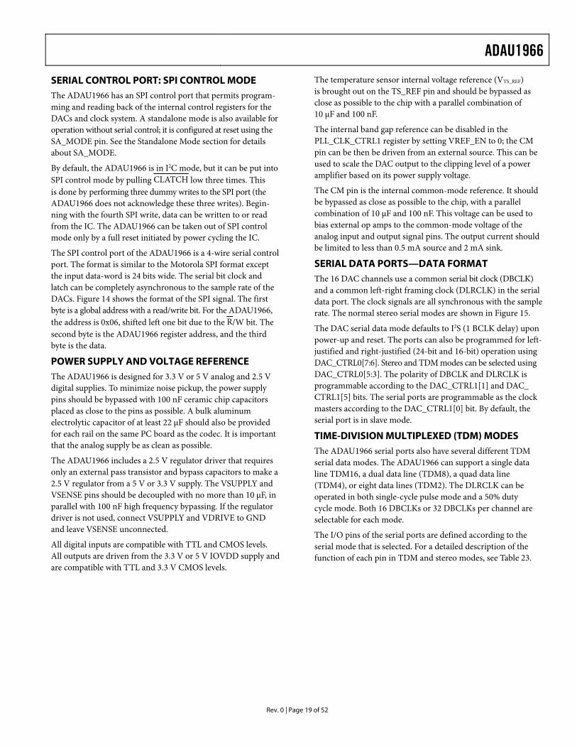
SERIAL DATA PORTS—DATA FORMAT The 16 DAC channels use a common serial bit clock (DBCLK) and a common left-right framing clock (DLRCLK) in the serial data port. The clock signals are all synchronous with the sample rate. The normal stereo serial modes are shown in Figure 15.
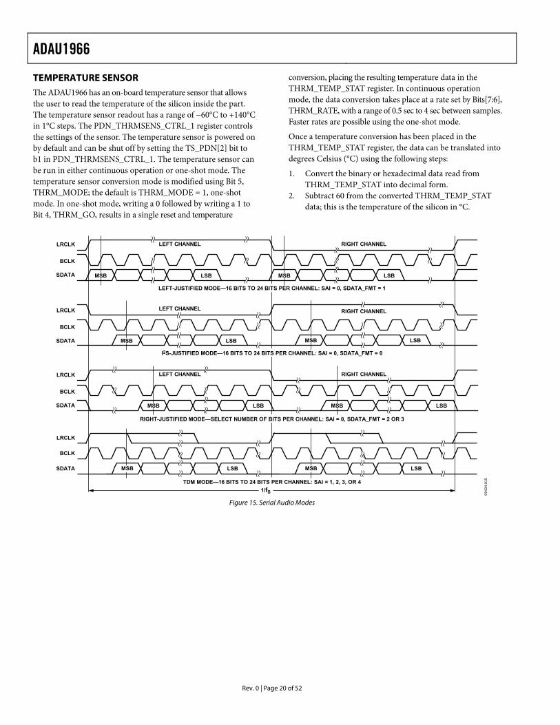
The DAC serial data mode defaults to I2S (1 BCLK delay) upon power-up and reset. The ports can also be programmed for left-justified and right-justified (24-bit and 16-bit) operation using DAC_CTRL0[7:6]. Stereo and TDM modes can be selected using DAC_CTRL0[5:3]. The polarity of DBCLK and DLRCLK is programmable according to the DAC_CTRL1[1] and DAC_ CTRL1[5] bits. The serial ports are programmable as the clock masters according to the DAC_CTRL1[0] bit. By default, the serial port is in slave mode.
TIME-DIVISION MULTIPLEXED (TDM) MODES The ADAU1966 serial ports also have several different TDM serial data modes. The ADAU1966 can support a single data line TDM16, a dual data line (TDM8), a quad data line (TDM4), or eight data lines (TDM2). The DLRCLK can be operated in both single-cycle pulse mode and a 50% duty cycle mode. Both 16 DBCLKs or 32 DBCLKs per channel are selectable for each mode.
The I/O pins of the serial ports are defined according to the serial mode that is selected. For a detailed description of the function of each pin in TDM and stereo modes, see Table 23.
ADAU1966
Rev. 0 | Page 20 of 52
TEMPERATURE SENSOR The ADAU1966 has an on-board temperature sensor that allows the user to read the temperature of the silicon inside the part. The temperature sensor readout has a range of −60°C to +140°C in 1°C steps. The PDN_THRMSENS_CTRL_1 register controls the settings of the sensor. The temperature sensor is powered on by default and can be shut off by setting the TS_PDN[2] bit to b1 in PDN_THRMSENS_CTRL_1. The temperature sensor can be run in either continuous operation or one-shot mode. The temperature sensor conversion mode is modified using Bit 5, THRM_MODE; the default is THRM_MODE = 1, one-shot mode. In one-shot mode, writing a 0 followed by writing a 1 to Bit 4, THRM_GO, results in a single reset and temperature
conversion, placing the resulting temperature data in the THRM_TEMP_STAT register. In continuous operation mode, the data conversion takes place at a rate set by Bits[7:6], THRM_RATE, with a range of 0.5 sec to 4 sec between samples. Faster rates are possible using the one-shot mode.
Once a temperature conversion has been placed in the THRM_TEMP_STAT register, the data can be translated into degrees Celsius (°C) using the following steps:
1. Convert the binary or hexadecimal data read from THRM_TEMP_STAT into decimal form.
2. Subtract 60 from the converted THRM_TEMP_STAT data; this is the temperature of the silicon in °C.
LRCLK
BCLK
SDATA
LRCLK
BCLK
SDATA
LRCLK
BCLK
SDATA LSB LSB
LSBLSB
LSB LSB
LEFT CHANNEL RIGHT CHANNEL
RIGHT CHANNELLEFT CHANNEL
LEFT CHANNEL RIGHT CHANNEL
MSB MSB
MSBMSB
MSB MSB
RIGHT-JUSTIFIED MODE—SELECT NUMBER OF BITS PER CHANNEL: SAI = 0, SDATA_FMT = 2 OR 3
TDM MODE—16 BITS TO 24 BITS PER CHANNEL: SAI = 1, 2, 3, OR 4
I2S-JUSTIFIED MODE—16 BITS TO 24 BITS PER CHANNEL: SAI = 0, SDATA_FMT = 0
LEFT-JUSTIFIED MODE—16 BITS TO 24 BITS PER CHANNEL: SAI = 0, SDATA_FMT = 1
LRCLK
BCLK
SDATA LSB LSBMSB MSB
1/fS 0943
4-01
5
Figure 15. Serial Audio Modes
ADAU1966
Rev. 0 | Page 21 of 52
DBCLK
DLRCLK
DSDATAxLEFT-JUSTIFIED
MODE
DSDATAxRIGHT-JUSTIFIED
MODE
DSDATAxI2S-JUSTIFIED
MODE
tDLH
tDBH
tDBL
tDLS
tDDS
MSB
MSB
MSB LSB
MSB – 1
tDDH
tDDS
tDDH
tDDS
tDDH tDDH
tDDS
0943
4-01
6
Figure 16. DAC Serial Timing
Table 23. Pin Function Changes in Different Serial Audio Interface Modes
Signal Stereo Modes (SAI = 0 or 1)
TDM4 Mode (SAI = 2)
TDM8 Mode (SAI = 3)
TDM16 Mode (SAI = 4)
DSDATA1 Channel 1/Channel 2 data in
Channel 1 to Channel 4 data in
Channel 1 to Channel 8 data in
Channel 1 to Channel 16 data in
DSDATA2 Channel 3/Channel 4 data in
Channel 5 to Channel 8 data in
Channel 9 to Channel 16 data in
Not used
DSDATA3 Channel 5/Channel 6 data in
Channel 9 to Channel 12 data in
Not used Not used
DSDATA4 Channel 7/Channel 8 data in
Channel 13 to Channel 16 data in
Not used Not used
DSDATA5 Channel 9/Channel 10 data in
Not used Not used Not used
DSDATA6 Channel 11/Channel 12 data in
Not used Not Used Not used
DSDATA7 Channel 13/Channel 14 data in
Not used Not used Not used
DSDATA8 Channel 15/Channel 16 data in
Not used Not used Not used
DLRCLK DLRCLK in/DLRCLK out TDM frame sync in/ TDM frame sync out
TDM frame sync in/ TDM frame sync out
TDM frame sync in/ TDM frame sync out
DBCLK DBCLK in/DBCLK out TDM DBCLK in/TDM DBCLK out
TDM DBCLK in/TDM DBCLK out
TDM DBCLK in/ TDM DBCLK out
Maximum Sample Rate 192 kHz 192 kHz 96 kHz 48 kHz
ADAU1966
Rev. 0 | Page 22 of 52
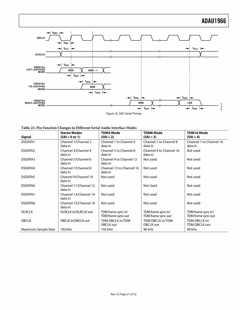
ADDITIONAL MODES The ADAU1966 offers several additional modes for board level design enhancements. To reduce the EMI in board level design, serial data can be transmitted without an explicit DBCLK. See Figure 17 for an example of a DAC TDM data transmission mode that does not require a high speed DBCLK or an external MCLK. This configuration is applicable when the ADAU1966 master clock is generated by the PLL with the DLRCLK as the PLL reference frequency.
To relax the requirement for the setup time of the ADAU1966 in cases of high speed TDM data transmission, the ADAU1966 can latch in the data using the falling edge of DBCLK; see the BCLK_EDGE bit in the DAC_CTRL1 register. This effectively dedicates the entire BCLK period to the setup time. This mode is useful in cases where the source has a large delay time in the serial data driver. Figure 18 shows this inverted DBCLK mode of data transmission.
DLRCLK
INTERNALDBCLK
DSDATAx
DLRCLK
INTERNALDBCLK
TDM-DSDATAx
32 BITS
0943
4-01
7
Figure 17. Serial DAC Data Transmission in TDM Format Without DBCLK
(Applicable Only If PLL Locks to DLRCLK)
DLRCLK
DBCLK
DSDATAx
DATA MUST BE VALIDAT THIS BCLK EDGE
MSB09
434-
018
Figure 18. Inverted DBCLK Mode in DAC Serial Data Transmission
(Applicable in Stereo and TDM, Useful for High Frequency TDM Transmission)
ADAU1966
Rev. 0 | Page 23 of 52
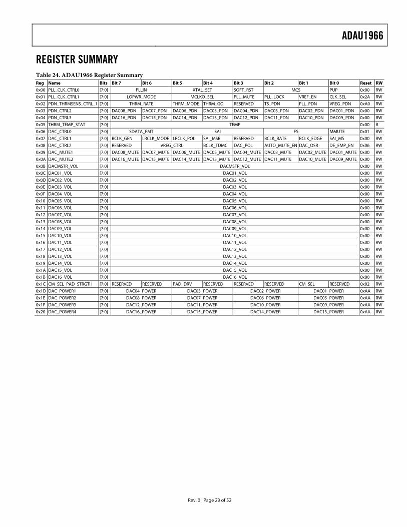
REGISTER SUMMARY Table 24. ADAU1966 Register Summary Reg Name Bits Bit 7 Bit 6 Bit 5 Bit 4 Bit 3 Bit 2 Bit 1 Bit 0 Reset RW
0x00 PLL_CLK_CTRL0 [7:0] PLLIN XTAL_SET SOFT_RST MCS PUP 0x00 RW
0x01 PLL_CLK_CTRL1 [7:0] LOPWR_MODE MCLKO_SEL PLL_MUTE PLL_LOCK VREF_EN CLK_SEL 0x2A RW
0x02 PDN_THRMSENS_CTRL_1 [7:0] THRM_RATE THRM_MODE THRM_GO RESERVED TS_PDN PLL_PDN VREG_PDN 0xA0 RW
0x03 PDN_CTRL2 [7:0] DAC08_PDN DAC07_PDN DAC06_PDN DAC05_PDN DAC04_PDN DAC03_PDN DAC02_PDN DAC01_PDN 0x00 RW
0x04 PDN_CTRL3 [7:0] DAC16_PDN DAC15_PDN DAC14_PDN DAC13_PDN DAC12_PDN DAC11_PDN DAC10_PDN DAC09_PDN 0x00 RW
0x05 THRM_TEMP_STAT [7:0] TEMP 0x00 R 0x06 DAC_CTRL0 [7:0] SDATA_FMT SAI FS MMUTE 0x01 RW
0x07 DAC_CTRL1 [7:0] BCLK_GEN LRCLK_MODE LRCLK_POL SAI_MSB RESERVED BCLK_RATE BCLK_EDGE SAI_MS 0x00 RW
0x08 DAC_CTRL2 [7:0] RESERVED VREG_CTRL BCLK_TDMC DAC_POL AUTO_MUTE_EN DAC_OSR DE_EMP_EN 0x06 RW
0x09 DAC_MUTE1 [7:0] DAC08_MUTE DAC07_MUTE DAC06_MUTE DAC05_MUTE DAC04_MUTE DAC03_MUTE DAC02_MUTE DAC01_MUTE 0x00 RW
0x0A DAC_MUTE2 [7:0] DAC16_MUTE DAC15_MUTE DAC14_MUTE DAC13_MUTE DAC12_MUTE DAC11_MUTE DAC10_MUTE DAC09_MUTE 0x00 RW
0x0B DACMSTR_VOL [7:0] DACMSTR_VOL 0x00 RW
0x0C DAC01_VOL [7:0] DAC01_VOL 0x00 RW
0x0D DAC02_VOL [7:0] DAC02_VOL 0x00 RW
0x0E DAC03_VOL [7:0] DAC03_VOL 0x00 RW
0x0F DAC04_VOL [7:0] DAC04_VOL 0x00 RW
0x10 DAC05_VOL [7:0] DAC05_VOL 0x00 RW
0x11 DAC06_VOL [7:0] DAC06_VOL 0x00 RW
0x12 DAC07_VOL [7:0] DAC07_VOL 0x00 RW
0x13 DAC08_VOL [7:0] DAC08_VOL 0x00 RW
0x14 DAC09_VOL [7:0] DAC09_VOL 0x00 RW
0x15 DAC10_VOL [7:0] DAC10_VOL 0x00 RW
0x16 DAC11_VOL [7:0] DAC11_VOL 0x00 RW
0x17 DAC12_VOL [7:0] DAC12_VOL 0x00 RW
0x18 DAC13_VOL [7:0] DAC13_VOL 0x00 RW
0x19 DAC14_VOL [7:0] DAC14_VOL 0x00 RW
0x1A DAC15_VOL [7:0] DAC15_VOL 0x00 RW
0x1B DAC16_VOL [7:0] DAC16_VOL 0x00 RW
0x1C CM_SEL_PAD_STRGTH [7:0] RESERVED RESERVED PAD_DRV RESERVED RESERVED RESERVED CM_SEL RESERVED 0x02 RW
0x1D DAC_POWER1 [7:0] DAC04_POWER DAC03_POWER DAC02_POWER DAC01_POWER 0xAA RW
0x1E DAC_POWER2 [7:0] DAC08_POWER DAC07_POWER DAC06_POWER DAC05_POWER 0xAA RW
0x1F DAC_POWER3 [7:0] DAC12_POWER DAC11_POWER DAC10_POWER DAC09_POWER 0xAA RW
0x20 DAC_POWER4 [7:0] DAC16_POWER DAC15_POWER DAC14_POWER DAC13_POWER 0xAA RW
ADAU1966
Rev. 0 | Page 24 of 52
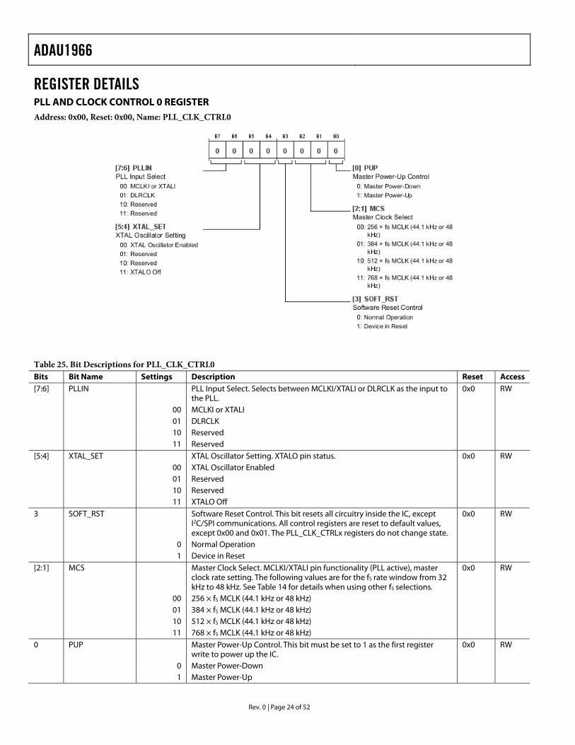
REGISTER DETAILS PLL AND CLOCK CONTROL 0 REGISTER Address: 0x00, Reset: 0x00, Name: PLL_CLK_CTRL0
Table 25. Bit Descriptions for PLL_CLK_CTRL0 Bits Bit Name Settings Description Reset Access [7:6] PLLIN PLL Input Select. Selects between MCLKI/XTALI or DLRCLK as the input to
the PLL. 0x0 RW
00 MCLKI or XTALI 01 DLRCLK 10 Reserved 11 Reserved [5:4] XTAL_SET XTAL Oscillator Setting. XTALO pin status. 0x0 RW 00 XTAL Oscillator Enabled 01 Reserved 10 Reserved 11 XTALO Off 3 SOFT_RST Software Reset Control. This bit resets all circuitry inside the IC, except
I2C/SPI communications. All control registers are reset to default values, except 0x00 and 0x01. The PLL_CLK_CTRLx registers do not change state.
0x0 RW
0 Normal Operation 1 Device in Reset [2:1] MCS Master Clock Select. MCLKI/XTALI pin functionality (PLL active), master
clock rate setting. The following values are for the fS rate window from 32 kHz to 48 kHz. See Table 14 for details when using other fS selections.
0x0 RW
00 256 × fS MCLK (44.1 kHz or 48 kHz) 01 384 × fS MCLK (44.1 kHz or 48 kHz) 10 512 × fS MCLK (44.1 kHz or 48 kHz) 11 768 × fS MCLK (44.1 kHz or 48 kHz) 0 PUP Master Power-Up Control. This bit must be set to 1 as the first register
write to power up the IC. 0x0 RW
0 Master Power-Down 1 Master Power-Up
ADAU1966
Rev. 0 | Page 25 of 52
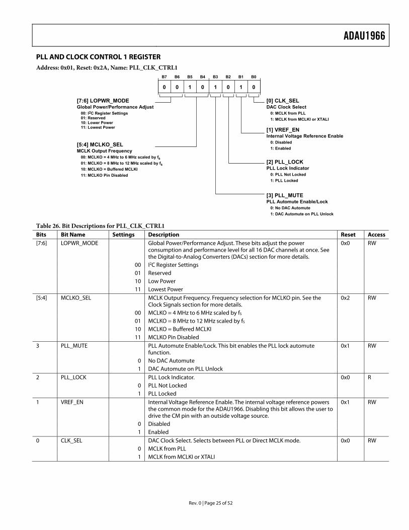
PLL AND CLOCK CONTROL 1 REGISTER Address: 0x01, Reset: 0x2A, Name: PLL_CLK_CTRL1
0
B7
0
B6
1
B5
0
B4
1
B3
0
B2
1
B1
0
B0
[0] CLK_SELDAC Clock Select
0: MCLK from PLL1: MCLK from MCLKI or XTALI
[1] VREF_ENInternal Voltage Reference Enable
0: Disabled1: Enabled
[2] PLL_LOCKPLL Lock Indicator
0: PLL Not Locked1: PLL Locked
[3] PLL_MUTEPLL Automute Enable/Lock
0: No DAC Automute1: DAC Automute on PLL Unlock
[7:6] LOPWR_MODEGlobal Power/Performance Adjust
00: I2C Register Settings01: Reserved10: Lower Power11: Lowest Power
[5:4] MCLKO_SELMCLK Output Frequency
00: MCLKO = 4 MHz to 6 MHz scaled by fs01: MCLKO = 8 MHz to 12 MHz scaled by fs10: MCLKO = Buffered MCLKI11: MCLKO Pin Disabled
Table 26. Bit Descriptions for PLL_CLK_CTRL1 Bits Bit Name Settings Description Reset Access [7:6] LOPWR_MODE Global Power/Performance Adjust. These bits adjust the power
consumption and performance level for all 16 DAC channels at once. See the Digital-to-Analog Converters (DACs) section for more details.
0x0 RW
00 I2C Register Settings 01 Reserved 10 Low Power 11 Lowest Power [5:4] MCLKO_SEL MCLK Output Frequency. Frequency selection for MCLKO pin. See the
Clock Signals section for more details. 0x2 RW
00 MCLKO = 4 MHz to 6 MHz scaled by fS 01 MCLKO = 8 MHz to 12 MHz scaled by fS 10 MCLKO = Buffered MCLKI 11 MCLKO Pin Disabled 3 PLL_MUTE PLL Automute Enable/Lock. This bit enables the PLL lock automute
function. 0x1 RW
0 No DAC Automute 1 DAC Automute on PLL Unlock 2 PLL_LOCK PLL Lock Indicator. 0x0 R 0 PLL Not Locked 1 PLL Locked 1 VREF_EN Internal Voltage Reference Enable. The internal voltage reference powers
the common mode for the ADAU1966. Disabling this bit allows the user to drive the CM pin with an outside voltage source.
0x1 RW
0 Disabled 1 Enabled 0 CLK_SEL DAC Clock Select. Selects between PLL or Direct MCLK mode. 0x0 RW 0 MCLK from PLL 1 MCLK from MCLKI or XTALI
ADAU1966
Rev. 0 | Page 26 of 52
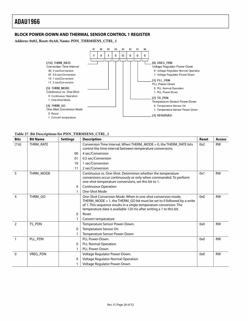
BLOCK POWER-DOWN AND THERMAL SENSOR CONTROL 1 REGISTER Address: 0x02, Reset: 0xA0, Name: PDN_THRMSENS_CTRL_1
Table 27. Bit Descriptions for PDN_THRMSENS_CTRL_1 Bits Bit Name Settings Description Reset Access [7:6] THRM_RATE Conversion Time Interval. When THERM_MODE = 0, the THERM_RATE bits
control the time interval between temperature conversions. 0x2 RW
00 4 sec/Conversion 01 0.5 sec/Conversion 10 1 sec/Conversion 11 2 sec/Conversion 5 THRM_MODE Continuous vs. One-Shot. Determines whether the temperature
conversions occur continuously or only when commanded. To perform one-shot temperature conversions, set this bit to 1.
0x1 RW
0 Continuous Operation 1 One-Shot Mode 4 THRM_GO One-Shot Conversion Mode. When in one-shot conversion mode,
THERM_MODE = 1, the THERM_GO bit must be set to 0 followed by a write of 1. This sequence results in a single temperature conversion. The temperature data is available 120 ms after writing a 1 to this bit.
0x0 RW
0 Reset 1 Convert temperature 2 TS_PDN Temperature Sensor Power-Down. 0x0 RW 0 Temperature Sensor On 1 Temperature Sensor Power-Down 1 PLL_PDN PLL Power-Down. 0x0 RW 0 PLL Normal Operation 1 PLL Power-Down 0 VREG_PDN Voltage Regulator Power-Down. 0x0 RW 0 Voltage Regulator Normal Operation 1 Voltage Regulator Power-Down
ADAU1966
Rev. 0 | Page 27 of 52
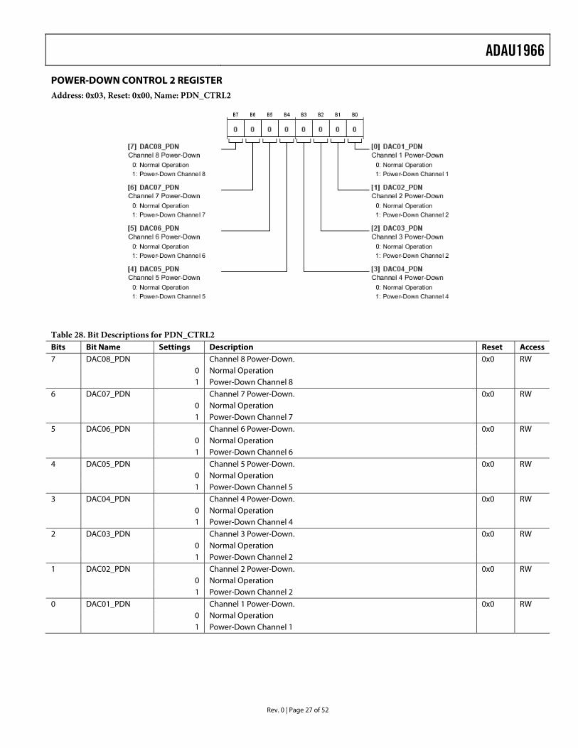
POWER-DOWN CONTROL 2 REGISTER Address: 0x03, Reset: 0x00, Name: PDN_CTRL2
Table 28. Bit Descriptions for PDN_CTRL2 Bits Bit Name Settings Description Reset Access 7 DAC08_PDN Channel 8 Power-Down. 0x0 RW 0 Normal Operation 1 Power-Down Channel 8 6 DAC07_PDN Channel 7 Power-Down. 0x0 RW 0 Normal Operation 1 Power-Down Channel 7 5 DAC06_PDN Channel 6 Power-Down. 0x0 RW 0 Normal Operation 1 Power-Down Channel 6 4 DAC05_PDN Channel 5 Power-Down. 0x0 RW 0 Normal Operation 1 Power-Down Channel 5 3 DAC04_PDN Channel 4 Power-Down. 0x0 RW 0 Normal Operation 1 Power-Down Channel 4 2 DAC03_PDN Channel 3 Power-Down. 0x0 RW 0 Normal Operation 1 Power-Down Channel 2 1 DAC02_PDN Channel 2 Power-Down. 0x0 RW 0 Normal Operation 1 Power-Down Channel 2 0 DAC01_PDN Channel 1 Power-Down. 0x0 RW 0 Normal Operation 1 Power-Down Channel 1
ADAU1966
Rev. 0 | Page 28 of 52
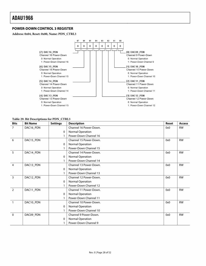
POWER-DOWN CONTROL 3 REGISTER Address: 0x04, Reset: 0x00, Name: PDN_CTRL3
Table 29. Bit Descriptions for PDN_CTRL3 Bits Bit Name Settings Description Reset Access 7 DAC16_PDN Channel 16 Power-Down. 0x0 RW 0 Normal Operation 1 Power-Down Channel 16 6 DAC15_PDN Channel 15 Power-Down. 0x0 RW 0 Normal Operation 1 Power-Down Channel 15 5 DAC14_PDN Channel 14 Power-Down. 0x0 RW 0 Normal Operation 1 Power-Down Channel 14 4 DAC13_PDN Channel 13 Power-Down. 0x0 RW 0 Normal Operation 1 Power-Down Channel 13 3 DAC12_PDN Channel 12 Power-Down. 0x0 RW 0 Normal Operation 1 Power-Down Channel 12 2 DAC11_PDN Channel 11 Power-Down. 0x0 RW 0 Normal Operation 1 Power-Down Channel 11 1 DAC10_PDN Channel 10 Power-Down. 0x0 RW 0 Normal Operation 1 Power-Down Channel 10 0 DAC09_PDN Channel 9 Power-Down. 0x0 RW 0 Normal Operation 1 Power-Down Channel 9
ADAU1966
Rev. 0 | Page 29 of 52
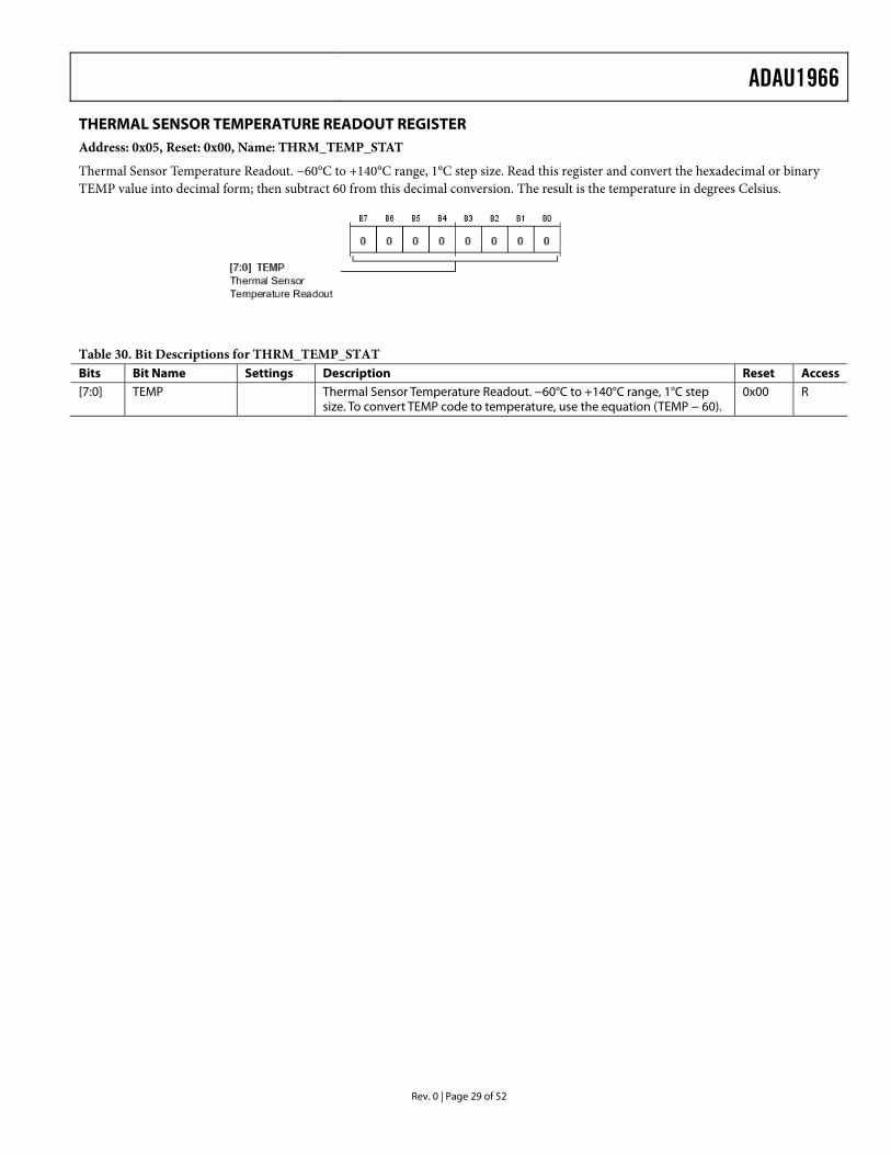
THERMAL SENSOR TEMPERATURE READOUT REGISTER Address: 0x05, Reset: 0x00, Name: THRM_TEMP_STAT
Thermal Sensor Temperature Readout. −60°C to +140°C range, 1°C step size. Read this register and convert the hexadecimal or binary TEMP value into decimal form; then subtract 60 from this decimal conversion. The result is the temperature in degrees Celsius.
Table 30. Bit Descriptions for THRM_TEMP_STAT Bits Bit Name Settings Description Reset Access [7:0] TEMP Thermal Sensor Temperature Readout. −60°C to +140°C range, 1°C step
size. To convert TEMP code to temperature, use the equation (TEMP − 60). 0x00 R
ADAU1966
Rev. 0 | Page 30 of 52
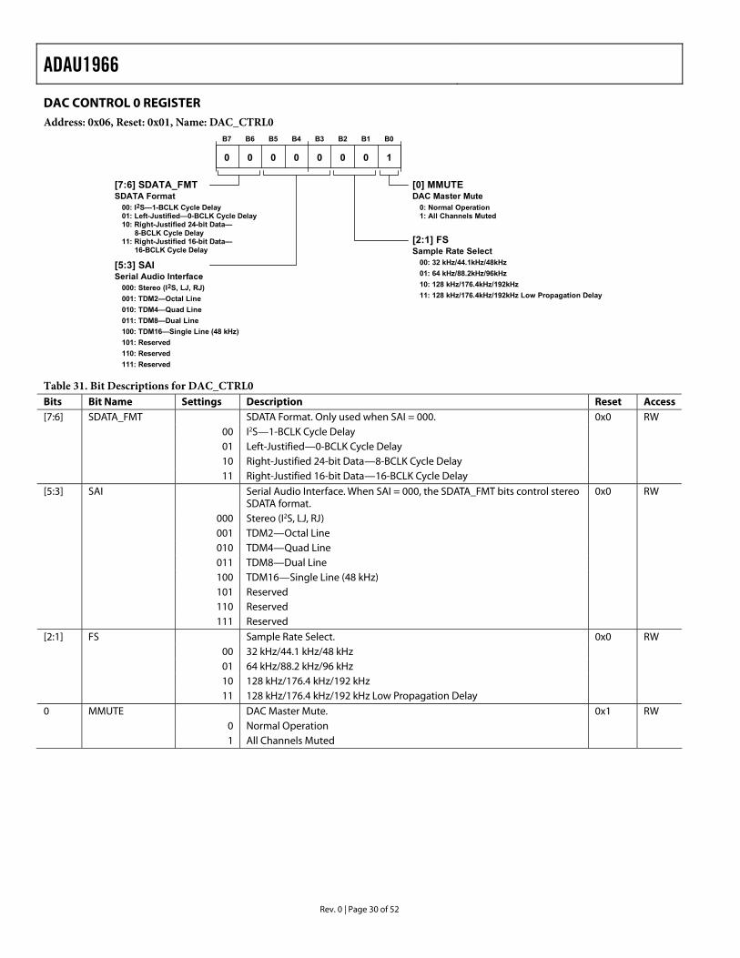
DAC CONTROL 0 REGISTER Address: 0x06, Reset: 0x01, Name: DAC_CTRL0
0
B7
0
B6
0
B5
0
B4
0
B3
0
B2
0
B1
1
B0
[7:6] SDATA_FMTSDATA Format
00: I2S—1-BCLK Cycle Delay01: Left-Justified—0-BCLK Cycle Delay10: Right-Justified 24-bit Data— 8-BCLK Cycle Delay11: Right-Justified 16-bit Data— 16-BCLK Cycle Delay
[5:3] SAISerial Audio Interface
000: Stereo (I2S, LJ, RJ)001: TDM2—Octal Line010: TDM4—Quad Line011: TDM8—Dual Line100: TDM16—Single Line (48 kHz)101: Reserved110: Reserved111: Reserved
[0] MMUTEDAC Master Mute
0: Normal Operation1: All Channels Muted
[2:1] FSSample Rate Select
00: 32 kHz/44.1kHz/48kHz01: 64 kHz/88.2kHz/96kHz10: 128 kHz/176.4kHz/192kHz11: 128 kHz/176.4kHz/192kHz Low Propagation Delay
Table 31. Bit Descriptions for DAC_CTRL0 Bits Bit Name Settings Description Reset Access [7:6] SDATA_FMT SDATA Format. Only used when SAI = 000. 0x0 RW 00 I2S—1-BCLK Cycle Delay 01 Left-Justified—0-BCLK Cycle Delay 10 Right-Justified 24-bit Data—8-BCLK Cycle Delay 11 Right-Justified 16-bit Data—16-BCLK Cycle Delay [5:3] SAI Serial Audio Interface. When SAI = 000, the SDATA_FMT bits control stereo
SDATA format. 0x0 RW
000 Stereo (I2S, LJ, RJ) 001 TDM2—Octal Line 010 TDM4—Quad Line 011 TDM8—Dual Line 100 TDM16—Single Line (48 kHz) 101 Reserved 110 Reserved 111 Reserved [2:1] FS Sample Rate Select. 0x0 RW 00 32 kHz/44.1 kHz/48 kHz 01 64 kHz/88.2 kHz/96 kHz 10 128 kHz/176.4 kHz/192 kHz 11 128 kHz/176.4 kHz/192 kHz Low Propagation Delay 0 MMUTE DAC Master Mute. 0x1 RW 0 Normal Operation 1 All Channels Muted
ADAU1966
Rev. 0 | Page 31 of 52
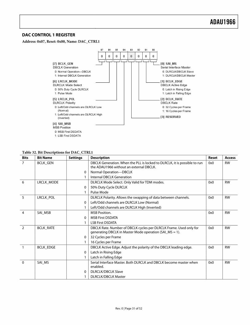
DAC CONTROL 1 REGISTER Address: 0x07, Reset: 0x00, Name: DAC_CTRL1
Table 32. Bit Descriptions for DAC_CTRL1 Bits Bit Name Settings Description Reset Access 7 BCLK_GEN DBCLK Generation. When the PLL is locked to DLRCLK, it is possible to run
the ADAU1966 without an external DBCLK. 0x0 RW
0 Normal Operation—DBCLK 1 Internal DBCLK Generation 6 LRCLK_MODE DLRCLK Mode Select. Only Valid for TDM modes. 0x0 RW 0 50% Duty Cycle DLRCLK 1 Pulse Mode 5 LRCLK_POL DLRCLK Polarity. Allows the swapping of data between channels. 0x0 RW 0 Left/Odd channels are DLRCLK Low (Normal) 1 Left/Odd channels are DLRCLK High (Inverted) 4 SAI_MSB MSB Position. 0x0 RW 0 MSB First DSDATA 1 LSB First DSDATA 2 BCLK_RATE DBCLK Rate. Number of DBCLK cycles per DLRCLK Frame. Used only for
generating DBCLK in Master Mode operation (SAI_MS = 1). 0x0 RW
0 32 Cycles per Frame 1 16 Cycles per Frame 1 BCLK_EDGE DBCLK Active Edge. Adjust the polarity of the DBCLK leading edge. 0x0 RW 0 Latch in Rising Edge 1 Latch in Falling Edge 0 SAI_MS Serial Interface Master. Both DLRCLK and DBCLK become master when
enabled. 0x0 RW
0 DLRCLK/DBCLK Slave 1 DLRCLK/DBCLK Master
ADAU1966
Rev. 0 | Page 32 of 52
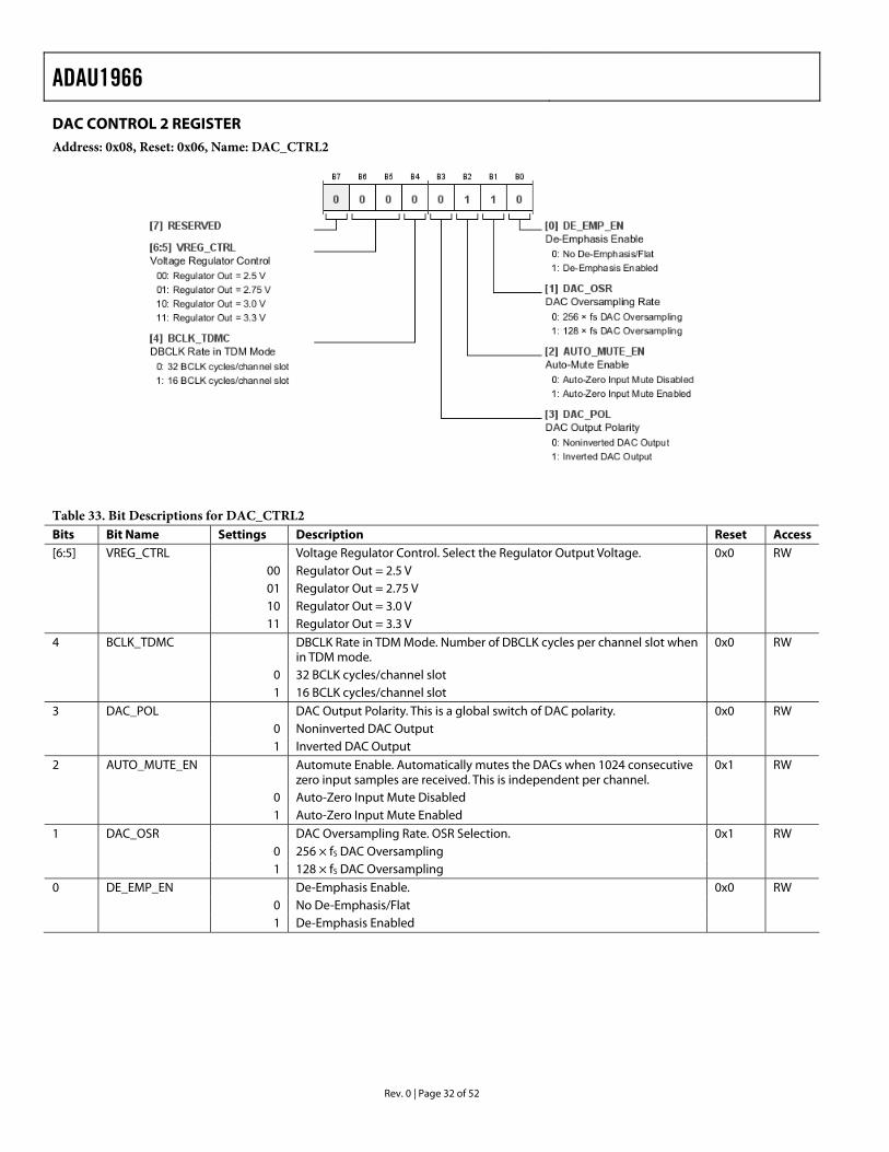
DAC CONTROL 2 REGISTER Address: 0x08, Reset: 0x06, Name: DAC_CTRL2
Table 33. Bit Descriptions for DAC_CTRL2 Bits Bit Name Settings Description Reset Access [6:5] VREG_CTRL Voltage Regulator Control. Select the Regulator Output Voltage. 0x0 RW 00 Regulator Out = 2.5 V 01 Regulator Out = 2.75 V 10 Regulator Out = 3.0 V 11 Regulator Out = 3.3 V 4 BCLK_TDMC DBCLK Rate in TDM Mode. Number of DBCLK cycles per channel slot when
in TDM mode. 0x0 RW
0 32 BCLK cycles/channel slot 1 16 BCLK cycles/channel slot 3 DAC_POL DAC Output Polarity. This is a global switch of DAC polarity. 0x0 RW 0 Noninverted DAC Output 1 Inverted DAC Output 2 AUTO_MUTE_EN Automute Enable. Automatically mutes the DACs when 1024 consecutive
zero input samples are received. This is independent per channel. 0x1 RW
0 Auto-Zero Input Mute Disabled 1 Auto-Zero Input Mute Enabled 1 DAC_OSR DAC Oversampling Rate. OSR Selection. 0x1 RW 0 256 × fS DAC Oversampling 1 128 × fS DAC Oversampling 0 DE_EMP_EN De-Emphasis Enable. 0x0 RW 0 No De-Emphasis/Flat 1 De-Emphasis Enabled
ADAU1966
Rev. 0 | Page 33 of 52
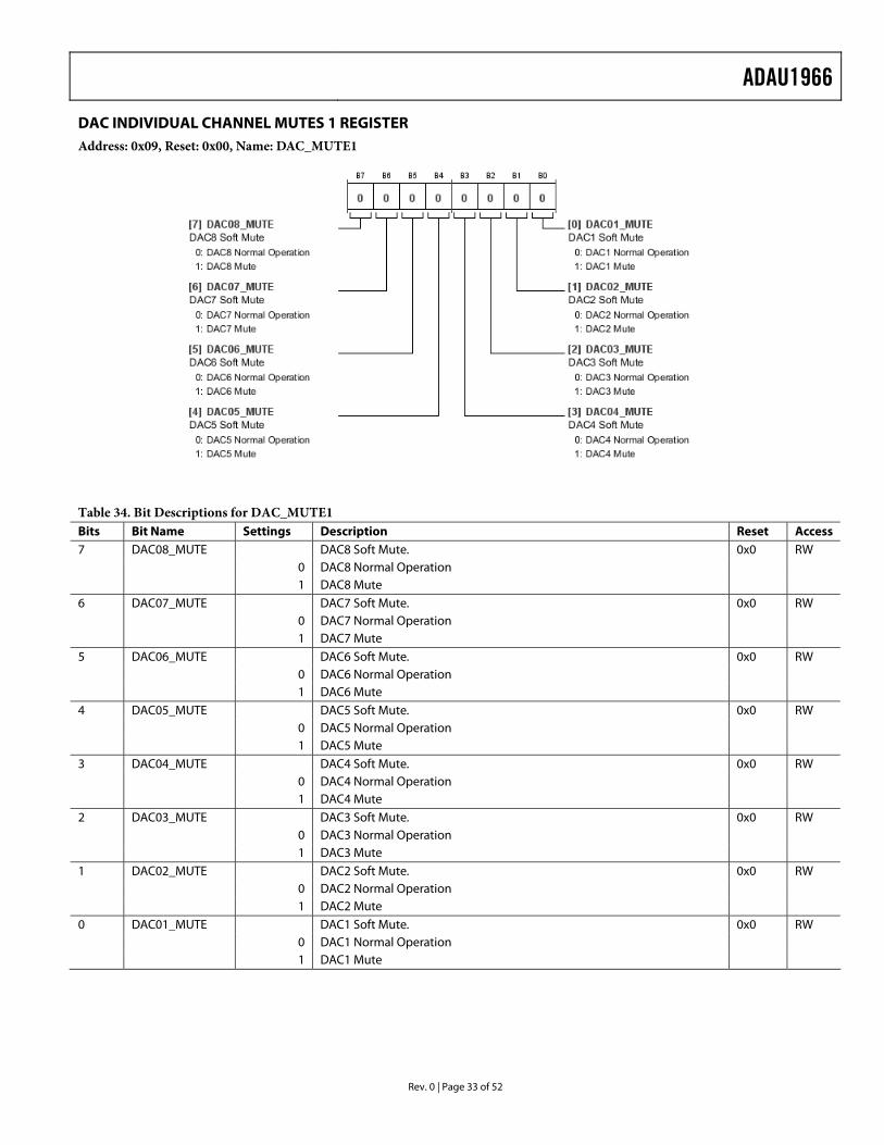
DAC INDIVIDUAL CHANNEL MUTES 1 REGISTER Address: 0x09, Reset: 0x00, Name: DAC_MUTE1
Table 34. Bit Descriptions for DAC_MUTE1 Bits Bit Name Settings Description Reset Access 7 DAC08_MUTE DAC8 Soft Mute. 0x0 RW 0 DAC8 Normal Operation 1 DAC8 Mute 6 DAC07_MUTE DAC7 Soft Mute. 0x0 RW 0 DAC7 Normal Operation 1 DAC7 Mute 5 DAC06_MUTE DAC6 Soft Mute. 0x0 RW 0 DAC6 Normal Operation 1 DAC6 Mute 4 DAC05_MUTE DAC5 Soft Mute. 0x0 RW 0 DAC5 Normal Operation 1 DAC5 Mute 3 DAC04_MUTE DAC4 Soft Mute. 0x0 RW 0 DAC4 Normal Operation 1 DAC4 Mute 2 DAC03_MUTE DAC3 Soft Mute. 0x0 RW 0 DAC3 Normal Operation 1 DAC3 Mute 1 DAC02_MUTE DAC2 Soft Mute. 0x0 RW 0 DAC2 Normal Operation 1 DAC2 Mute 0 DAC01_MUTE DAC1 Soft Mute. 0x0 RW 0 DAC1 Normal Operation 1 DAC1 Mute
ADAU1966
Rev. 0 | Page 34 of 52
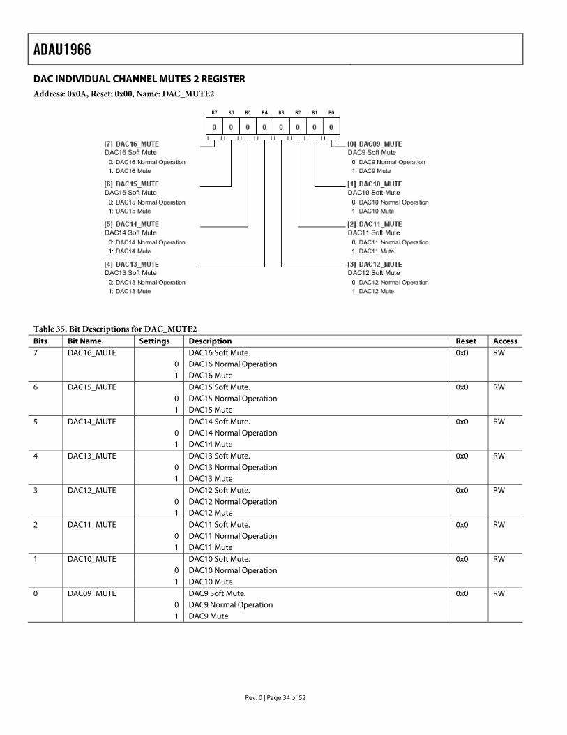
DAC INDIVIDUAL CHANNEL MUTES 2 REGISTER Address: 0x0A, Reset: 0x00, Name: DAC_MUTE2
Table 35. Bit Descriptions for DAC_MUTE2 Bits Bit Name Settings Description Reset Access 7 DAC16_MUTE DAC16 Soft Mute. 0x0 RW 0 DAC16 Normal Operation 1 DAC16 Mute 6 DAC15_MUTE DAC15 Soft Mute. 0x0 RW 0 DAC15 Normal Operation 1 DAC15 Mute 5 DAC14_MUTE DAC14 Soft Mute. 0x0 RW 0 DAC14 Normal Operation 1 DAC14 Mute 4 DAC13_MUTE DAC13 Soft Mute. 0x0 RW 0 DAC13 Normal Operation 1 DAC13 Mute 3 DAC12_MUTE DAC12 Soft Mute. 0x0 RW 0 DAC12 Normal Operation 1 DAC12 Mute 2 DAC11_MUTE DAC11 Soft Mute. 0x0 RW 0 DAC11 Normal Operation 1 DAC11 Mute 1 DAC10_MUTE DAC10 Soft Mute. 0x0 RW 0 DAC10 Normal Operation 1 DAC10 Mute 0 DAC09_MUTE DAC9 Soft Mute. 0x0 RW 0 DAC9 Normal Operation 1 DAC9 Mute
ADAU1966
Rev. 0 | Page 35 of 52
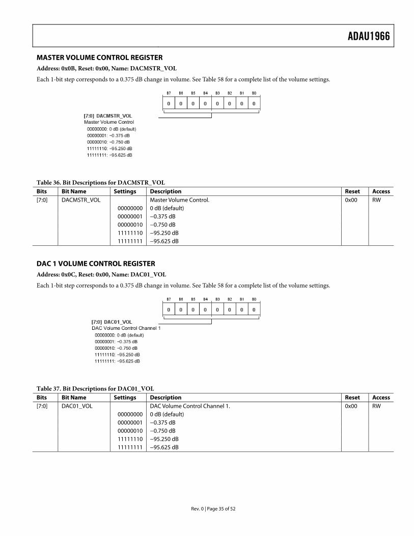
MASTER VOLUME CONTROL REGISTER Address: 0x0B, Reset: 0x00, Name: DACMSTR_VOL
Each 1-bit step corresponds to a 0.375 dB change in volume. See Table 58 for a complete list of the volume settings.
Table 36. Bit Descriptions for DACMSTR_VOL Bits Bit Name Settings Description Reset Access [7:0] DACMSTR_VOL Master Volume Control. 0x00 RW 00000000 0 dB (default) 00000001 −0.375 dB 00000010 −0.750 dB 11111110 −95.250 dB 11111111 −95.625 dB
DAC 1 VOLUME CONTROL REGISTER Address: 0x0C, Reset: 0x00, Name: DAC01_VOL
Each 1-bit step corresponds to a 0.375 dB change in volume. See Table 58 for a complete list of the volume settings.
Table 37. Bit Descriptions for DAC01_VOL Bits Bit Name Settings Description Reset Access [7:0] DAC01_VOL DAC Volume Control Channel 1. 0x00 RW 00000000 0 dB (default) 00000001 −0.375 dB 00000010 −0.750 dB 11111110 −95.250 dB 11111111 −95.625 dB

ADAU1966
Rev. 0 | Page 36 of 52
DAC 2 VOLUME CONTROL REGISTER Address: 0x0D, Reset: 0x00, Name: DAC02_VOL
Each 1-bit step corresponds to a 0.375 dB change in volume. See Table 58 for a complete list of the volume settings.
Table 38. Bit Descriptions for DAC02_VOL Bits Bit Name Settings Description Reset Access [7:0] DAC02_VOL DAC Volume Control Channel 2. 0x00 RW 00000000 0 dB (default) 00000001 −0.375 dB 00000010 −0.750 dB 11111110 −95.250 dB 11111111 −95.625 dB
DAC 3 VOLUME CONTROL REGISTER Address: 0x0E, Reset: 0x00, Name: DAC03_VOL
Each 1-bit step corresponds to a 0.375 dB change in volume. See Table 58 for a complete list of the volume settings.
Table 39. Bit Descriptions for DAC03_VOL Bits Bit Name Settings Description Reset Access [7:0] DAC03_VOL DAC Volume Control Channel 3. 0x00 RW 00000000 0 dB (default) 00000001 −0.375 dB 00000010 −0.750 dB 11111110 −95.250 dB 11111111 −95.625 dB

ADAU1966
Rev. 0 | Page 37 of 52
DAC 4 VOLUME CONTROL REGISTER Address: 0x0F, Reset: 0x00, Name: DAC04_VOL
Each 1-bit step corresponds to a 0.375 dB change in volume. See Table 58 for a complete list of the volume settings.
Table 40. Bit Descriptions for DAC04_VOL Bits Bit Name Settings Description Reset Access [7:0] DAC04_VOL DAC Volume Control Channel 4. 0x00 RW 00000000 0 dB (default) 00000001 −0.375 dB 00000010 −0.750 dB 11111110 −95.250 dB 11111111 −95.625 dB
DAC 5 VOLUME CONTROL REGISTER Address: 0x10, Reset: 0x00, Name: DAC05_VOL
Each 1-bit step corresponds to a 0.375 dB change in volume. See Table 58 for a complete list of the volume settings.
Table 41. Bit Descriptions for DAC05_VOL Bits Bit Name Settings Description Reset Access [7:0] DAC05_VOL DAC Volume Control Channel 5. 0x00 RW 00000000 0 dB (default) 00000001 −0.375 dB 00000010 −0.750 dB 11111110 −95.250 dB 11111111 −95.625 dB
ADAU1966
Rev. 0 | Page 38 of 52
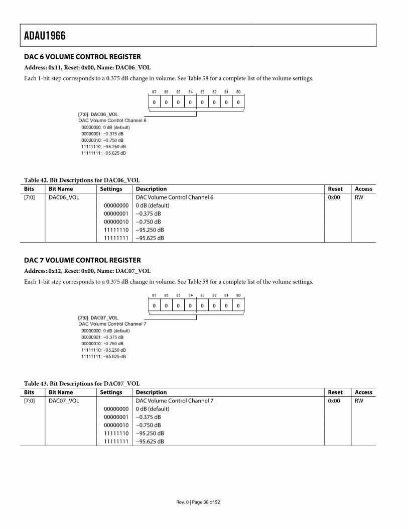
DAC 6 VOLUME CONTROL REGISTER Address: 0x11, Reset: 0x00, Name: DAC06_VOL
Each 1-bit step corresponds to a 0.375 dB change in volume. See Table 58 for a complete list of the volume settings.
Table 42. Bit Descriptions for DAC06_VOL Bits Bit Name Settings Description Reset Access [7:0] DAC06_VOL DAC Volume Control Channel 6. 0x00 RW 00000000 0 dB (default) 00000001 −0.375 dB 00000010 −0.750 dB 11111110 −95.250 dB 11111111 −95.625 dB
DAC 7 VOLUME CONTROL REGISTER Address: 0x12, Reset: 0x00, Name: DAC07_VOL
Each 1-bit step corresponds to a 0.375 dB change in volume. See Table 58 for a complete list of the volume settings.
Table 43. Bit Descriptions for DAC07_VOL Bits Bit Name Settings Description Reset Access [7:0] DAC07_VOL DAC Volume Control Channel 7. 0x00 RW 00000000 0 dB (default) 00000001 −0.375 dB 00000010 −0.750 dB 11111110 −95.250 dB 11111111 −95.625 dB

ADAU1966
Rev. 0 | Page 39 of 52
DAC 8 VOLUME CONTROL REGISTER Address: 0x13, Reset: 0x00, Name: DAC08_VOL
Each 1-bit step corresponds to a 0.375 dB change in volume. See Table 58 for a complete list of the volume settings.
Table 44. Bit Descriptions for DAC08_VOL Bits Bit Name Settings Description Reset Access [7:0] DAC08_VOL DAC Volume Control Channel 8. 0x00 RW 00000000 0 dB (default) 00000001 −0.375 dB 00000010 −0.750 dB 11111110 −95.250 dB 11111111 −95.625 dB
DAC 9 VOLUME CONTROL REGISTER Address: 0x14, Reset: 0x00, Name: DAC09_VOL
Each 1-bit step corresponds to a 0.375 dB change in volume. See Table 58 for a complete list of the volume settings.
Table 45. Bit Descriptions for DAC09_VOL Bits Bit Name Settings Description Reset Access [7:0] DAC09_VOL DAC Volume Control Channel 9. 0x00 RW 00000000 0 dB (default) 00000001 −0.375 dB 00000010 −0.750 dB 11111110 −95.250 dB 11111111 −95.625 dB

ADAU1966
Rev. 0 | Page 40 of 52
DAC 10 VOLUME CONTROL REGISTER Address: 0x15, Reset: 0x00, Name: DAC10_VOL
Each 1-bit step corresponds to a 0.375 dB change in volume. See Table 58 for a complete list of the volume settings.
Table 46. Bit Descriptions for DAC10_VOL Bits Bit Name Settings Description Reset Access [7:0] DAC10_VOL DAC Volume Control Channel 10. 0x00 RW 00000000 0 dB (default) 00000001 −0.375 dB 00000010 −0.750 dB 11111110 −95.250 dB 11111111 −95.625 dB
DAC 11 VOLUME CONTROL REGISTER Address: 0x16, Reset: 0x00, Name: DAC11_VOL
Each 1-bit step corresponds to a 0.375 dB change in volume. See Table 58 for a complete list of the volume settings.
Table 47. Bit Descriptions for DAC11_VOL Bits Bit Name Settings Description Reset Access [7:0] DAC11_VOL DAC Volume Control Channel 11. 0x00 RW 00000000 0 dB (default) 00000001 −0.375 dB 00000010 −0.750 dB 11111110 −95.250 dB 11111111 −95.625 dB
ADAU1966
Rev. 0 | Page 41 of 52
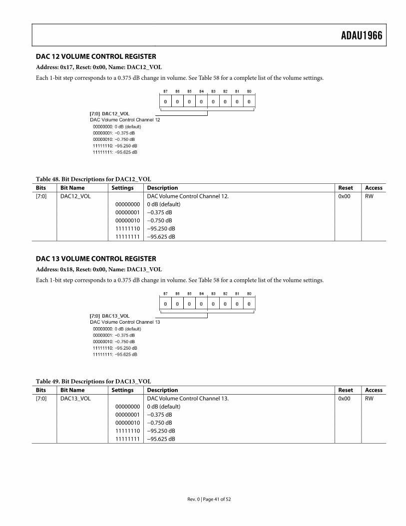
DAC 12 VOLUME CONTROL REGISTER Address: 0x17, Reset: 0x00, Name: DAC12_VOL
Each 1-bit step corresponds to a 0.375 dB change in volume. See Table 58 for a complete list of the volume settings.
Table 48. Bit Descriptions for DAC12_VOL Bits Bit Name Settings Description Reset Access [7:0] DAC12_VOL DAC Volume Control Channel 12. 0x00 RW 00000000 0 dB (default) 00000001 −0.375 dB 00000010 −0.750 dB 11111110 −95.250 dB 11111111 −95.625 dB
DAC 13 VOLUME CONTROL REGISTER Address: 0x18, Reset: 0x00, Name: DAC13_VOL
Each 1-bit step corresponds to a 0.375 dB change in volume. See Table 58 for a complete list of the volume settings.
Table 49. Bit Descriptions for DAC13_VOL Bits Bit Name Settings Description Reset Access [7:0] DAC13_VOL DAC Volume Control Channel 13. 0x00 RW 00000000 0 dB (default) 00000001 −0.375 dB 00000010 −0.750 dB 11111110 −95.250 dB 11111111 −95.625 dB
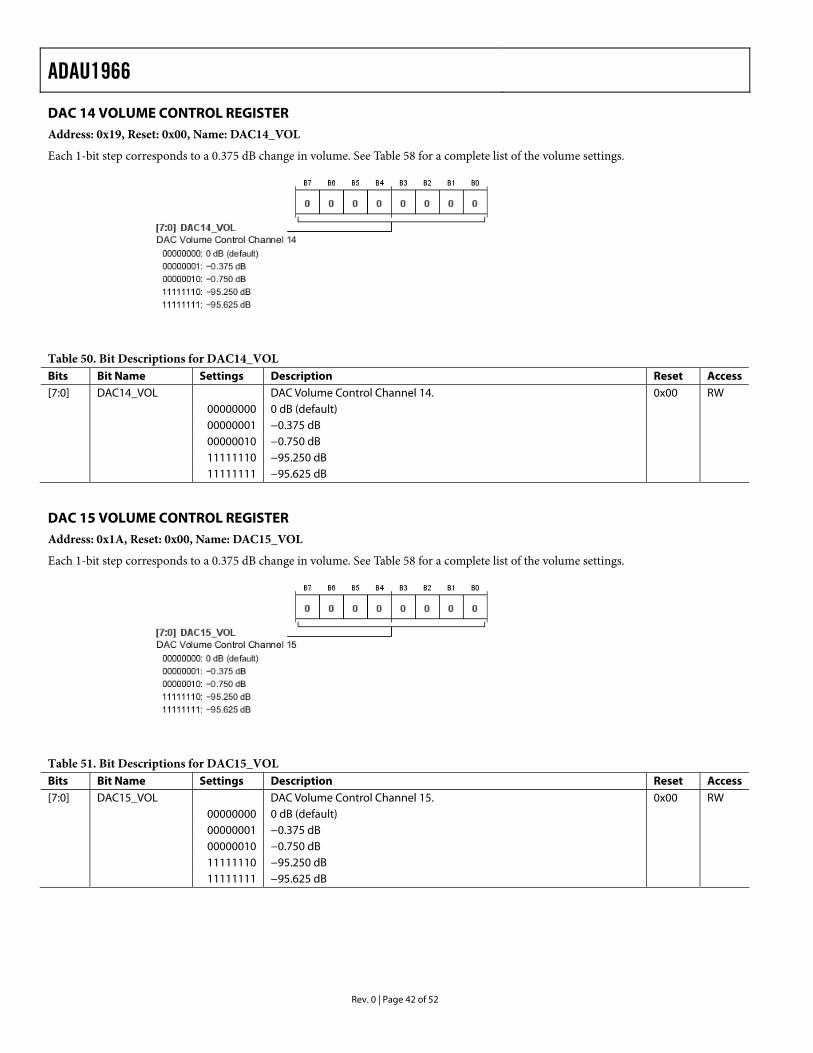
ADAU1966
Rev. 0 | Page 42 of 52
DAC 14 VOLUME CONTROL REGISTER Address: 0x19, Reset: 0x00, Name: DAC14_VOL
Each 1-bit step corresponds to a 0.375 dB change in volume. See Table 58 for a complete list of the volume settings.
Table 50. Bit Descriptions for DAC14_VOL Bits Bit Name Settings Description Reset Access [7:0] DAC14_VOL DAC Volume Control Channel 14. 0x00 RW 00000000 0 dB (default) 00000001 −0.375 dB 00000010 −0.750 dB 11111110 −95.250 dB 11111111 −95.625 dB
DAC 15 VOLUME CONTROL REGISTER Address: 0x1A, Reset: 0x00, Name: DAC15_VOL
Each 1-bit step corresponds to a 0.375 dB change in volume. See Table 58 for a complete list of the volume settings.
Table 51. Bit Descriptions for DAC15_VOL Bits Bit Name Settings Description Reset Access [7:0] DAC15_VOL DAC Volume Control Channel 15. 0x00 RW 00000000 0 dB (default) 00000001 −0.375 dB 00000010 −0.750 dB 11111110 −95.250 dB 11111111 −95.625 dB
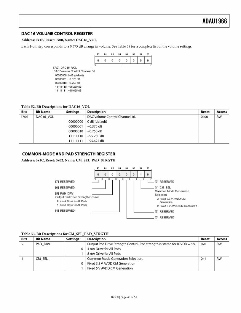
ADAU1966
Rev. 0 | Page 43 of 52
DAC 16 VOLUME CONTROL REGISTER Address: 0x1B, Reset: 0x00, Name: DAC16_VOL
Each 1-bit step corresponds to a 0.375 dB change in volume. See Table 58 for a complete list of the volume settings.
Table 52. Bit Descriptions for DAC16_VOL Bits Bit Name Settings Description Reset Access [7:0] DAC16_VOL DAC Volume Control Channel 16. 0x00 RW 00000000 0 dB (default) 00000001 −0.375 dB 00000010 −0.750 dB 11111110 −95.250 dB 11111111 −95.625 dB
COMMON-MODE AND PAD STRENGTH REGISTER Address: 0x1C, Reset: 0x02, Name: CM_SEL_PAD_STRGTH
Table 53. Bit Descriptions for CM_SEL_PAD_STRGTH Bits Bit Name Settings Description Reset Access 5 PAD_DRV Output Pad Drive Strength Control. Pad strength is stated for IOVDD = 5 V. 0x0 RW 0 4 mA Drive for All Pads 1 8 mA Drive for All Pads 1 CM_SEL Common Mode Generation Selection. 0x1 RW 0 Fixed 3.3 V AVDD CM Generation 1 Fixed 5 V AVDD CM Generation
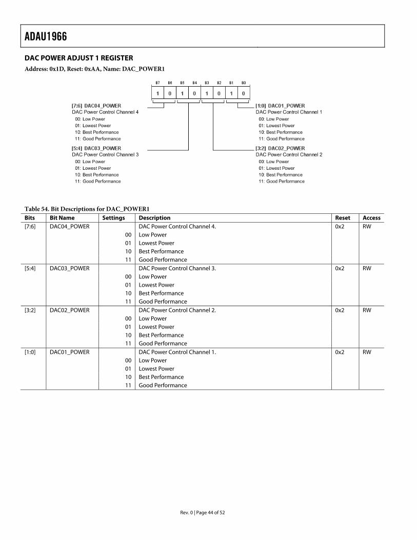
ADAU1966
Rev. 0 | Page 44 of 52
DAC POWER ADJUST 1 REGISTER Address: 0x1D, Reset: 0xAA, Name: DAC_POWER1
Table 54. Bit Descriptions for DAC_POWER1 Bits Bit Name Settings Description Reset Access [7:6] DAC04_POWER DAC Power Control Channel 4. 0x2 RW 00 Low Power 01 Lowest Power 10 Best Performance 11 Good Performance [5:4] DAC03_POWER DAC Power Control Channel 3. 0x2 RW 00 Low Power 01 Lowest Power 10 Best Performance 11 Good Performance [3:2] DAC02_POWER DAC Power Control Channel 2. 0x2 RW 00 Low Power 01 Lowest Power 10 Best Performance 11 Good Performance [1:0] DAC01_POWER DAC Power Control Channel 1. 0x2 RW 00 Low Power 01 Lowest Power 10 Best Performance 11 Good Performance
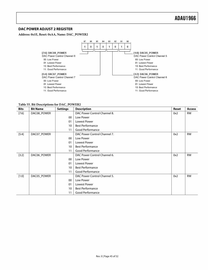
ADAU1966
Rev. 0 | Page 45 of 52
DAC POWER ADJUST 2 REGISTER Address: 0x1E, Reset: 0xAA, Name: DAC_POWER2
Table 55. Bit Descriptions for DAC_POWER2 Bits Bit Name Settings Description Reset Access [7:6] DAC08_POWER DAC Power Control Channel 8. 0x2 RW 00 Low Power 01 Lowest Power 10 Best Performance 11 Good Performance [5:4] DAC07_POWER DAC Power Control Channel 7. 0x2 RW 00 Low Power 01 Lowest Power 10 Best Performance 11 Good Performance [3:2] DAC06_POWER DAC Power Control Channel 6. 0x2 RW 00 Low Power 01 Lowest Power 10 Best Performance 11 Good Performance [1:0] DAC05_POWER DAC Power Control Channel 5. 0x2 RW 00 Low Power 01 Lowest Power 10 Best Performance 11 Good Performance

ADAU1966
Rev. 0 | Page 46 of 52
DAC POWER ADJUST 3 REGISTER Address: 0x1F, Reset: 0xAA, Name: DAC_POWER3
Table 56. Bit Descriptions for DAC_POWER3 Bits Bit Name Settings Description Reset Access [7:6] DAC12_POWER DAC Power Control Channel 12. 0x2 RW 00 Low Power 01 Lowest Power 10 Best Performance 11 Good Performance [5:4] DAC11_POWER DAC Power Control Channel 11. 0x2 RW 00 Low Power 01 Lowest Power 10 Best Performance 11 Good Performance [3:2] DAC10_POWER DAC Power Control Channel 10. 0x2 RW 00 Low Power 01 Lowest Power 10 Best Performance 11 Good Performance [1:0] DAC09_POWER DAC Power Control Channel 9. 0x2 RW 00 Low Power 01 Lowest Power 10 Best Performance 11 Good Performance

ADAU1966
Rev. 0 | Page 47 of 52
DAC POWER ADJUST 4 REGISTER Address: 0x20, Reset: 0xAA, Name: DAC_POWER4
Table 57. Bit Descriptions for DAC_POWER4 Bits Bit Name Settings Description Reset Access [7:6] DAC16_POWER DAC Power Control Channel 16. 0x2 RW 00 Low Power 01 Lowest Power 10 Best Performance 11 Good Performance [5:4] DAC15_POWER DAC Power Control Channel 15. 0x2 RW 00 Low Power 01 Lowest Power 10 Best Performance 11 Good Performance [3:2] DAC14_POWER DAC Power Control Channel 14. 0x2 RW 00 Low Power 01 Lowest Power 10 Best Performance 11 Good Performance [1:0] DAC13_POWER DAC Power Control Channel 13. 0x2 RW 00 Low Power 01 Lowest Power 10 Best Performance 11 Good Performance
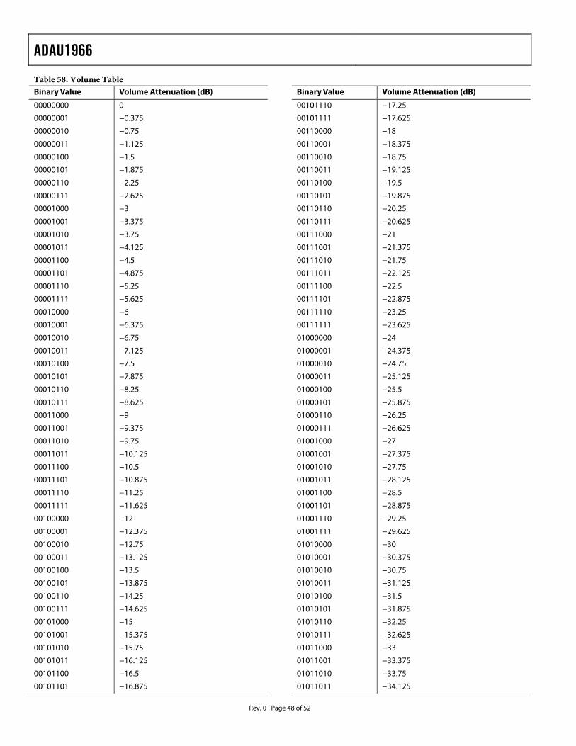
ADAU1966
Rev. 0 | Page 48 of 52
Table 58. Volume Table Binary Value Volume Attenuation (dB)
00000000 0
00000001 −0.375
00000010 −0.75
00000011 −1.125
00000100 −1.5
00000101 −1.875
00000110 −2.25
00000111 −2.625
00001000 −3
00001001 −3.375
00001010 −3.75
00001011 −4.125
00001100 −4.5
00001101 −4.875
00001110 −5.25
00001111 −5.625
00010000 −6
00010001 −6.375
00010010 −6.75
00010011 −7.125
00010100 −7.5
00010101 −7.875
00010110 −8.25
00010111 −8.625
00011000 −9
00011001 −9.375
00011010 −9.75
00011011 −10.125
00011100 −10.5
00011101 −10.875
00011110 −11.25
00011111 −11.625
00100000 −12
00100001 −12.375
00100010 −12.75
00100011 −13.125
00100100 −13.5
00100101 −13.875
00100110 −14.25
00100111 −14.625
00101000 −15
00101001 −15.375
00101010 −15.75
00101011 −16.125
00101100 −16.5
00101101 −16.875
Binary Value Volume Attenuation (dB)
00101110 −17.25
00101111 −17.625
00110000 −18
00110001 −18.375
00110010 −18.75
00110011 −19.125
00110100 −19.5
00110101 −19.875
00110110 −20.25
00110111 −20.625
00111000 −21
00111001 −21.375
00111010 −21.75
00111011 −22.125
00111100 −22.5
00111101 −22.875
00111110 −23.25
00111111 −23.625
01000000 −24
01000001 −24.375
01000010 −24.75
01000011 −25.125
01000100 −25.5
01000101 −25.875
01000110 −26.25
01000111 −26.625
01001000 −27
01001001 −27.375
01001010 −27.75
01001011 −28.125
01001100 −28.5
01001101 −28.875
01001110 −29.25
01001111 −29.625
01010000 −30
01010001 −30.375
01010010 −30.75
01010011 −31.125
01010100 −31.5
01010101 −31.875
01010110 −32.25
01010111 −32.625
01011000 −33
01011001 −33.375
01011010 −33.75
01011011 −34.125
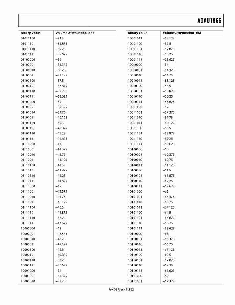
ADAU1966
Rev. 0 | Page 49 of 52
Binary Value Volume Attenuation (dB)
01011100 −34.5
01011101 −34.875
01011110 −35.25
01011111 −35.625
01100000 −36
01100001 −36.375
01100010 −36.75
01100011 −37.125
01100100 −37.5
01100101 −37.875
01100110 −38.25
01100111 −38.625
01101000 −39
01101001 −39.375
01101010 −39.75
01101011 −40.125
01101100 −40.5
01101101 −40.875
01101110 −41.25
01101111 −41.625
01110000 −42
01110001 −42.375
01110010 −42.75
01110011 −43.125
01110100 −43.5
01110101 −43.875
01110110 −44.25
01110111 −44.625
01111000 −45
01111001 −45.375
01111010 −45.75
01111011 −46.125
01111100 −46.5
01111101 −46.875
01111110 −47.25
01111111 −47.625
10000000 −48
10000001 −48.375
10000010 −48.75
10000011 −49.125
10000100 −49.5
10000101 −49.875
10000110 −50.25
10000111 −50.625
10001000 −51
10001001 −51.375
10001010 −51.75
Binary Value Volume Attenuation (dB)
10001011 −52.125
10001100 −52.5
10001101 −52.875
10001110 −53.25
10001111 −53.625
10010000 −54
10010001 −54.375
10010010 −54.75
10010011 −55.125
10010100 −55.5
10010101 −55.875
10010110 −56.25
10010111 −56.625
10011000 −57
10011001 −57.375
10011010 −57.75
10011011 −58.125
10011100 −58.5
10011101 −58.875
10011110 −59.25
10011111 −59.625
10100000 −60
10100001 −60.375
10100010 −60.75
10100011 −61.125
10100100 −61.5
10100101 −61.875
10100110 −62.25
10100111 −62.625
10101000 −63
10101001 −63.375
10101010 −63.75
10101011 −64.125
10101100 −64.5
10101101 −64.875
10101110 −65.25
10101111 −65.625
10110000 −66
10110001 −66.375
10110010 −66.75
10110011 −67.125
10110100 −67.5
10110101 −67.875
10110110 −68.25
10110111 −68.625
10111000 −69
10111001 −69.375
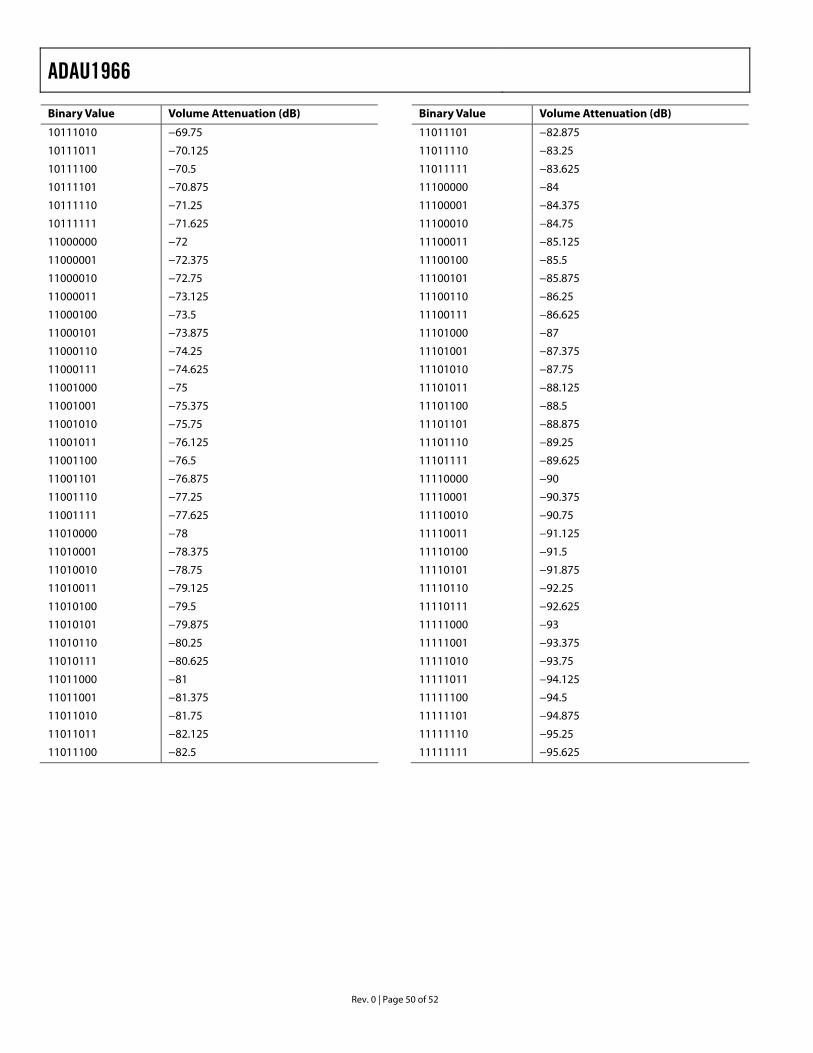
ADAU1966
Rev. 0 | Page 50 of 52
Binary Value Volume Attenuation (dB)
10111010 −69.75
10111011 −70.125
10111100 −70.5
10111101 −70.875
10111110 −71.25
10111111 −71.625
11000000 −72
11000001 −72.375
11000010 −72.75
11000011 −73.125
11000100 −73.5
11000101 −73.875
11000110 −74.25
11000111 −74.625
11001000 −75
11001001 −75.375
11001010 −75.75
11001011 −76.125
11001100 −76.5
11001101 −76.875
11001110 −77.25
11001111 −77.625
11010000 −78
11010001 −78.375
11010010 −78.75
11010011 −79.125
11010100 −79.5
11010101 −79.875
11010110 −80.25
11010111 −80.625
11011000 −81
11011001 −81.375
11011010 −81.75
11011011 −82.125
11011100 −82.5
Binary Value Volume Attenuation (dB)
11011101 −82.875
11011110 −83.25
11011111 −83.625
11100000 −84
11100001 −84.375
11100010 −84.75
11100011 −85.125
11100100 −85.5
11100101 −85.875
11100110 −86.25
11100111 −86.625
11101000 −87
11101001 −87.375
11101010 −87.75
11101011 −88.125
11101100 −88.5
11101101 −88.875
11101110 −89.25
11101111 −89.625
11110000 −90
11110001 −90.375
11110010 −90.75
11110011 −91.125
11110100 −91.5
11110101 −91.875
11110110 −92.25
11110111 −92.625
11111000 −93
11111001 −93.375
11111010 −93.75
11111011 −94.125
11111100 −94.5
11111101 −94.875
11111110 −95.25
11111111 −95.625
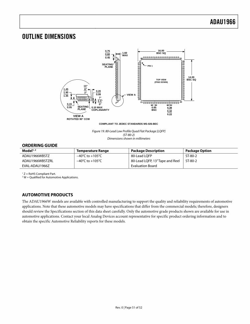
ADAU1966
Rev. 0 | Page 51 of 52
OUTLINE DIMENSIONS
1.451.401.35
0.150.05
61601
80
20 4121 40
TOP VIEW(PINS DOWN)
PIN 1SEATING
PLANE
VIEW A
1.60MAX
0.750.600.45
0.200.09
0.10 MAXCOPLANARITY
VIEW AROTATED 90° CCW
SEATINGPLANE
10°6°2°
7°3.5°0°
14.00BSC SQ
16.00BSC SQ
0.65BSC
0.380.320.22
COMPLIANT TO JEDEC STANDARDS MS-026-BEC
Figure 19. 80-Lead Low Profile Quad Flat Package [LQFP]
(ST-80-2) Dimensions shown in millimeters
ORDERING GUIDE Model1, 2 Temperature Range Package Description Package Option ADAU1966WBSTZ −40°C to +105°C 80-Lead LQFP ST-80-2 ADAU1966WBSTZRL −40°C to +105°C 80-Lead LQFP, 13” Tape and Reel ST-80-2 EVAL-ADAU1966Z Evaluation Board 1 Z = RoHS Compliant Part. 2 W = Qualified for Automotive Applications.
AUTOMOTIVE PRODUCTS The ADAU1966W models are available with controlled manufacturing to support the quality and reliability requirements of automotive applications. Note that these automotive models may have specifications that differ from the commercial models; therefore, designers should review the Specifications section of this data sheet carefully. Only the automotive grade products shown are available for use in automotive applications. Contact your local Analog Devices account representative for specific product ordering information and to obtain the specific Automotive Reliability reports for these models.
ADAU1966
Rev. 0 | Page 52 of 52
NOTES
I2C refers to a communications protocol originally developed by Philips Semiconductors (now NXP Semiconductors).
©2011 Analog Devices, Inc. All rights reserved. Trademarks and registered trademarks are the property of their respective owners. D09434-0-9/11(0)