Embed Size (px)
Citation preview
SLUS272C − FEBRUARY 2000 − REVISED JUNE 2003
1www.ti.com
FEATURES BiCMOS Version of UC3846 Family
1.4-mA Maximum Operating Current
100-µA Maximum Startup Current
±0.5-A Peak Output Current
125-ns Circuit Delay
Easier Parallelability
Improved Benefits of Current Mode Control
DESCRIPTION
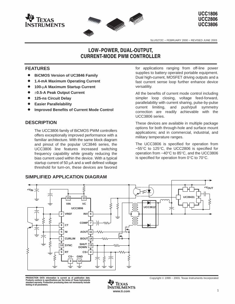
The UCC3806 family of BiCMOS PWM controllersoffers exceptionally improved performance with afamiliar architecture. With the same block diagramand pinout of the popular UC3846 series, theUCC3806 line features increased switchingfrequency capability while greatly reducing thebias current used within the device. With a typicalstartup current of 50 µA and a well defined voltagethreshold for turn-on, these devices are favored
for applications ranging from off-line powersupplies to battery operated portable equipment.Dual high-current, MOSFET driving outputs and afast current sense loop further enhance deviceversatility.
All the benefits of current mode control includingsimpler loop closing, voltage feed-forward,parallelability with current sharing, pulse-by-pulsecurrent limiting, and push/pull symmetrycorrection are readily achievable with theUCC3806 series.
These devices are available in multiple packageoptions for both through-hole and surface mountapplications; and in commercial, industrial, andmilitary temperature ranges.
The UCC3806 is specified for operation from−55°C to 125°C, the UCC2806 is specified foroperation from −40°C to 85°C, and the UCC3806is specified for operation from 0°C to 70°C.
SIMPLIFIED APPLICATION DIAGRAM
2
8
5
1
6
11
14
15
INV
AOUT
BOUT
VREF
CT
NI
CURLIM
UCC3806
10
9
SYNC
RT 4CS+
VIN
15 13
VC
7COMP
UCC3612
CS−
3 12
GND
UC39431
+VIN+VOUT
SHUTDOWN
! "#$ ! %#&'" ($) (#"! " !%$""! %$ *$ $! $+! !#$!!(( ,-) (#" %"$!!. ($! $"$!!'- "'#($$!. '' %$$!)
Copyright 1999 − 2003, Texas Instruments Incorporated
SLUS272C − FEBRUARY 2000 − REVISED JUNE 2003
2 www.ti.com
These devices have limited built-in ESD protection. The leads should be shorted together or the device placed in conductive foamduring storage or handling to prevent electrostatic damage to the MOS gates.
ABSOLUTE MAXIMUM RATINGSover operating free-air temperature range unless otherwise noted(1)
UCx806 UNIT
Supply voltage, VIN VIN, low impedance 15 V
Supply current, IIN VIN, high impedance 25 mA
Output supply voltage VC 18 V
Continuous source or sink ± 200
Output currentGate drive ± 500
mAOutput currentSYNC ± 30
mA
COMP ± 10 to −(self-limiting)
Analog input voltage range CS−, CS+, NI, INV, SHUTDOWN −0.3 to (VIN + 0.3) V
Storage temperature, Tstg −65 to 150 °C
Operating temperature, TJ −55 to 150 °C
Lead temperature, Tsol, 1,6 mm (1/16 inch) from case for 10 seconds 300 °C(1) Stresses beyond those listed under “absolute maximum ratings” may cause permanent damage to the device. These are stress ratings only,
and functional operation of the device at these or any other conditions beyond those indicated under “recommended operating conditions” isnot implied. Exposure to absolute-maximum-rated conditions for extended periods may affect device reliability. All voltages are with respect toGND. Currents are positive into and negative out of, the specified terminal.
RECOMMENDED OPERATING CONDITIONSMIN NOM MAX UNIT
Input voltage, VIN 8.0 14.5 V
UCC1806 −55 125
Operating junction temperature, TJ UCC2806 −40 85 °COperating junction temperature, TJUCC3806 0 70
C
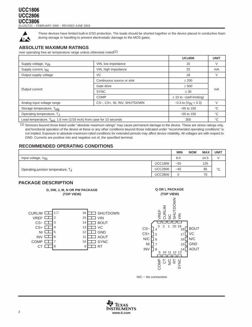
PACKAGE DESCRIPTION
1
2
3
4
5
6
78
16
15
14
13
12
11
109
CURLIMVREF
CS−CS+
NIINV
COMPCT
SHUTDOWNVINBOUTVCGNDAOUTSYNCRT
D, DW, J, M, N OR PW PACKAGE(TOP VIEW)
3 2 1 20 19
9 10 11 12 13
4
5
6
7
8
18
17
16
15
14
BOUTVCN/CGNDAOUT
CS−CS+N/C
NIINV
Q OR L PACKAGE(TOP VIEW)
VR
EF
CU
RLI
MN
CR
TS
YN
CS
HU
TD
OW
NV
IN
CO
MP
CT
N/C
N/C − No connection
SLUS272C − FEBRUARY 2000 − REVISED JUNE 2003
3www.ti.com
ORDERING INFORMATION
PACKAGED DEVICES TA = TJDESIGNATOR TYPE OPTION QUANTITY − 55°C to 125°C − 40°C to 85°C 0°C to 70°C
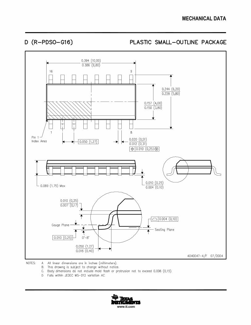
D SOIC−16Tube 40 – UCC2806D –
D SOIC−16Reeled 2,500 – UCC2806DTR –
DW SOICW−16Tube 40 – UCC2806DW UCC3806DW
DW SOICW−16Reeled 2,000 – UCC2806DWTR UCC3806DWTR
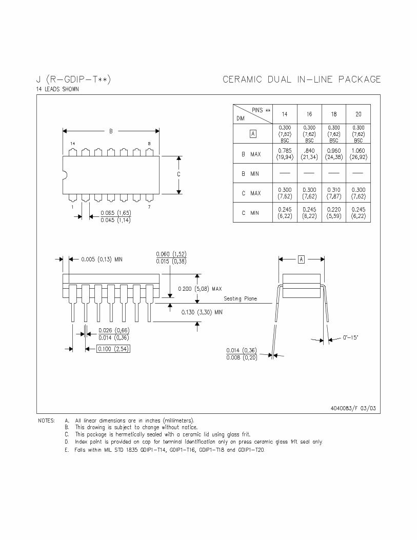
J CDIP−16 Tube 25 UCC1806J UCC2806J UCC3806J
L CLCC−20 Tube 55 UCC1806L – –
M SSOP−16 Reeled 2,500 – UCC2806MTR –
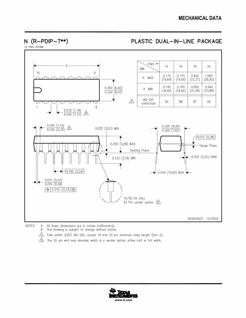
N PDIP−16 Tube 25 – UCC2806N UCC3806N
PW TSSOP−16Tube 90 – UCC2806PW UCC3806PW
PW TSSOP−16Reeled 2,000 – UCC2806PWTR UCC3806PWTR
Q PLCC−20Tube 46 – UCC2806Q UCC3806Q
Q PLCC−20Reeled 1,000 – UCC2806QTR UCC3806QTR
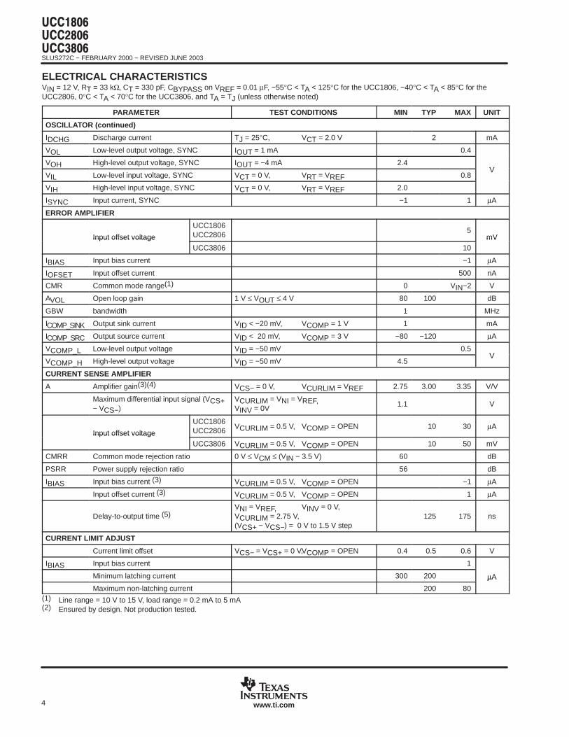
ELECTRICAL CHARACTERISTICSVIN = 12 V, RT = 33 kΩ, CT = 330 pF, CBYPASS on VREF = 0.01 µF, −55°C < TA < 125°C for the UCC1806, −40°C < TA < 85°C for theUCC2806, 0°C < TA < 70°C for the UCC3806, and TA = TJ (unless otherwise noted)
PARAMETER TEST CONDITIONS MIN TYP MAX UNIT
REFERENCE
VREF Supply, UVLO, turn-on
UCC1806UCC2806
5.02 5.10 5.17VVREF Supply, UVLO, turn-on
UCC3806 5.00 5.10 5.20
V
Load regulation 0.2 mA ≤ IOUT ≤ 5 mA 3 25mV
Total output variation (1)(2) Line, load, temperature −150 150mV
Output noise voltage (2) 10 Hz ≤ fOSC ≤ 10 kHz, TJ = 25°C 70 µV
Long term stability (2) TA = 125°C, 1000 hours 5 25 mV
Output short circuit −10 −30 mA
OSCILLATOR
Initial accuracy TJ = 25°C 42 47 52 kHz
Temperature stability (2) T(min) ≤ TA ≤ T(max) 2%
Amplitude 2.35 V
tDELAY Delay-to-output time, SYNC
UCC1806UCC2806
VCT = 0 V, VRT = VREF 0.8 V ≤ VSYNC ≤ 2.0 V
50 125
nstDELAY Delay-to-output time, SYNCUCC3806
VCT = 0 V, VRT = VREF 0.8 V ≤ VSYNC ≤ 2.0 V
50 100ns
SLUS272C − FEBRUARY 2000 − REVISED JUNE 2003
4 www.ti.com
ELECTRICAL CHARACTERISTICSVIN = 12 V, RT = 33 kΩ, CT = 330 pF, CBYPASS on VREF = 0.01 µF, −55°C < TA < 125°C for the UCC1806, −40°C < TA < 85°C for theUCC2806, 0°C < TA < 70°C for the UCC3806, and TA = TJ (unless otherwise noted)
PARAMETER TEST CONDITIONS MIN TYP MAX UNIT
OSCILLATOR (continued)
IDCHG Discharge current TJ = 25°C, VCT = 2.0 V 2 mA
VOL Low-level output voltage, SYNC IOUT = 1 mA 0.4
VOH High-level output voltage, SYNC IOUT = −4 mA 2.4V
VIL Low-level input voltage, SYNC VCT = 0 V, VRT = VREF 0.8V
VIH High-level input voltage, SYNC VCT = 0 V, VRT = VREF 2.0
ISYNC Input current, SYNC −1 1 µA
ERROR AMPLIFIER
Input offset voltage
UCC1806UCC2806
5mVInput offset voltage
UCC3806 10
mV
IBIAS Input bias current −1 µA
IOFSET Input offset current 500 nA
CMR Common mode range(1) 0 VIN−2 V
AVOL Open loop gain 1 V ≤ VOUT ≤ 4 V 80 100 dB
GBW bandwidth 1 MHz
ICOMP_SINK Output sink current VID < −20 mV, VCOMP = 1 V 1 mA
ICOMP_SRC Output source current VID < 20 mV, VCOMP = 3 V −80 −120 µA
VCOMP_L Low-level output voltage VID = −50 mV 0.5V
VCOMP_H High-level output voltage VID = −50 mV 4.5V
CURRENT SENSE AMPLIFIER
A Amplifier gain(3)(4) VCS− = 0 V, VCURLIM = VREF 2.75 3.00 3.35 V/V
Maximum differential input signal (VCS+− VCS−)
VCURLIM = VNI = VREF, VINV = 0V
1.1 V
Input offset voltage
UCC1806UCC2806
VCURLIM = 0.5 V, VCOMP = OPEN 10 30 µAInput offset voltage
UCC3806 VCURLIM = 0.5 V, VCOMP = OPEN 10 50 mV
CMRR Common mode rejection ratio 0 V ≤ VCM ≤ (VIN − 3.5 V) 60 dB
PSRR Power supply rejection ratio 56 dB
IBIAS Input bias current (3) VCURLIM = 0.5 V, VCOMP = OPEN −1 µA
Input offset current (3) VCURLIM = 0.5 V, VCOMP = OPEN 1 µA
Delay-to-output time (5)VNI = VREF, VINV = 0 V,VCURLIM = 2.75 V, (VCS+ − VCS−) = 0 V to 1.5 V step
125 175 ns
CURRENT LIMIT ADJUST
Current limit offset VCS− = VCS+ = 0 V, VCOMP = OPEN 0.4 0.5 0.6 V
IBIAS Input bias current 1
Minimum latching current 300 200 µA
Maximum non-latching current 200 80
µA
(1) Line range = 10 V to 15 V, load range = 0.2 mA to 5 mA(2) Ensured by design. Not production tested.
SLUS272C − FEBRUARY 2000 − REVISED JUNE 2003
5www.ti.com
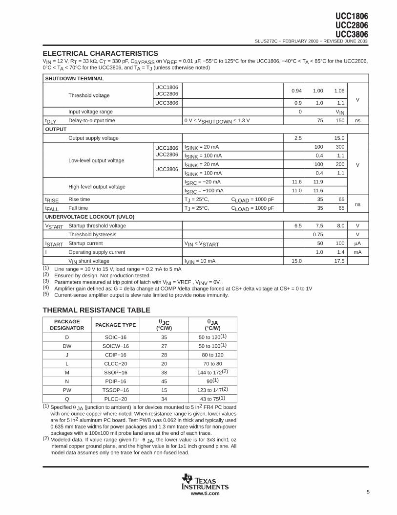
ELECTRICAL CHARACTERISTICSVIN = 12 V, RT = 33 kΩ, CT = 330 pF, CBYPASS on VREF = 0.01 µF, −55°C to 125°C for the UCC1806, −40°C < TA < 85°C for the UCC2806,0°C < TA < 70°C for the UCC3806, and TA = TJ (unless otherwise noted)
SHUTDOWN TERMINAL
Threshold voltage
UCC1806UCC2806
0.94 1.00 1.06
VThreshold voltage
UCC3806 0.9 1.0 1.1V
Input voltage range 0 VIN
tDLY Delay-to-output time 0 V ≤ VSHUTDOWN ≤ 1.3 V 75 150 ns
OUTPUT
Output supply voltage 2.5 15.0
UCC1806 ISINK = 20 mA 100 300
Low-level output voltage
UCC1806UCC2806 ISINK = 100 mA 0.4 1.1
Low-level output voltage
UCC3806ISINK = 20 mA 100 200 V
UCC3806ISINK = 100 mA 0.4 1.1
V
High-level output voltageISRC = −20 mA 11.6 11.9
High-level output voltageISRC = −100 mA 11.0 11.6
tRISE Rise time TJ = 25°C, CLOAD = 1000 pF 35 65ns
tFALL Fall time TJ = 25°C, CLOAD = 1000 pF 35 65ns
UNDERVOLTAGE LOCKOUT (UVLO)
VSTART Startup threshold voltage 6.5 7.5 8.0 V
Threshold hysteresis 0.75 V
ISTART Startup current VIN < VSTART 50 100 µA
I Operating supply current 1.0 1.4 mA
VIN shunt voltage IVIN = 10 mA 15.0 17.5(1) Line range = 10 V to 15 V, load range = 0.2 mA to 5 mA(2) Ensured by design. Not production tested.(3) Parameters measured at trip point of latch with VNI = VREF , VINV = 0V.(4) Amplifier gain defined as: G = delta change at COMP /delta change forced at CS+ delta voltage at CS+ = 0 to 1V(5) Current-sense amplifier output is slew rate limited to provide noise immunity.
THERMAL RESISTANCE TABLE
PACKAGEDESIGNATOR PACKAGE TYPE
θJC(°C/W)
θJA(°C/W)
D SOIC−16 35 50 to 120(1)
DW SOICW−16 27 50 to 100(1)
J CDIP−16 28 80 to 120
L CLCC−20 20 70 to 80
M SSOP−16 38 144 to 172(2)
N PDIP−16 45 90(1)
PW TSSOP−16 15 123 to 147(2)
Q PLCC−20 34 43 to 75(1)
(1) Specified θ JA (junction to ambient) is for devices mounted to 5 in2 FR4 PC boardwith one ounce copper where noted. When resistance range is given, lower valuesare for 5 in2 aluminum PC board. Test PWB was 0.062 in thick and typically used0.635 mm trace widths for power packages and 1.3 mm trace widths for non-powerpackages with a 100x100 mil probe land area at the end of each trace.
(2) Modeled data. If value range given for θ JA, the lower value is for 3x3 inch1 ozinternal copper ground plane, and the higher value is for 1x1 inch ground plane. Allmodel data assumes only one trace for each non-fused lead.

SLUS272C − FEBRUARY 2000 − REVISED JUNE 2003
6 www.ti.com
TERMINAL FUNCTIONS
TERMINAL
PACKAGESI/O DESCRIPTION
NAME D/DW/J/M/N/PW L,Q
I/O DESCRIPTION
AOUT 11 14O High-current gate drive for the external MOSFETs
BOUT 14 18O High-current gate drive for the external MOSFETs
COMP 7 9 O Output of the error amplifier
CS− 3 4 I Inverting input of the 3×, differential current sense amplifier
CS+ 4 5 I Non-inverting input of the 3×, differential current sense amplifier
CT 8 10 I Oscillator timing capacitor connection point
CURLIM 1 2 IPrograms the primary current limit threshold that determins latching or retry after anovercurrent situation
GND 12 15 − Reference ground and power ground for all functions of this device
INV 6 8 I Inverting input of the error amplifier.
NI 5 7 I Non-nverting input of the error amplifier.
RT 9 12 I Connection point for the oscillator timing resistor
SHUTDOWN 16 20 IProvided for enhanced protection. When SHUTDOWN is driven above 1 V, AOUT andBOUT are forced low.
SYNC 10 13 I/O Allows providing external synchronization with TTL compatible thresholds.
VC 13 17 I Input supply connection for the FET drive outputs.
VIN 15 19 I Input supply connection for this device.
VREF 2 3 O Reference output.
DETAILED PIN DESCRIPTIONS
AOUT and BOUT: AOUT and BOUT provide alternating high current gate drive for the external MOSFETs. Dutycycle can be varied from 0% to 50% where minimum dead time is a function of CT. Both outputs use MOStransistor switches with inherent anti-parallel body diodes to clamp voltage swings to the supply rails, allowingoperation without the use of clamp diodes.
COMP: COMP is the output of the error amplifier and the input of the PWM comparator. The error amplifier isa low output impedance, 2-MHz operational amplifier which allows sinking or sourcing of current at the COMPpin. The error amplifier is internally current limited, so that zero duty cycle can be commanded by externallyforcing COMP to GND.
CS−: CS− is the inverting input of the 3× differential current sense amplifier.
CS+: CS+ is the non-inverting input of the 3× differential current sense amplifier.
CT: CT is the oscillator timing capacitor connection point, which is charged by the current set by RT. CT isdischarged to GND through a 2.6-mA current sink. This causes a linear discharge of CT to 0 V which theninitiates the next switching cycle. Dead time occurs during the discharge of CT, forcing AOUT and BOUT low.Switching frequency (fS) and dead time (tD) are approximated by:
fS 1
2 RT CT tDand tD 961 CT
(1)
SLUS272C − FEBRUARY 2000 − REVISED JUNE 2003
7www.ti.com
DETAILED PIN DESCRIPTIONS (continued)
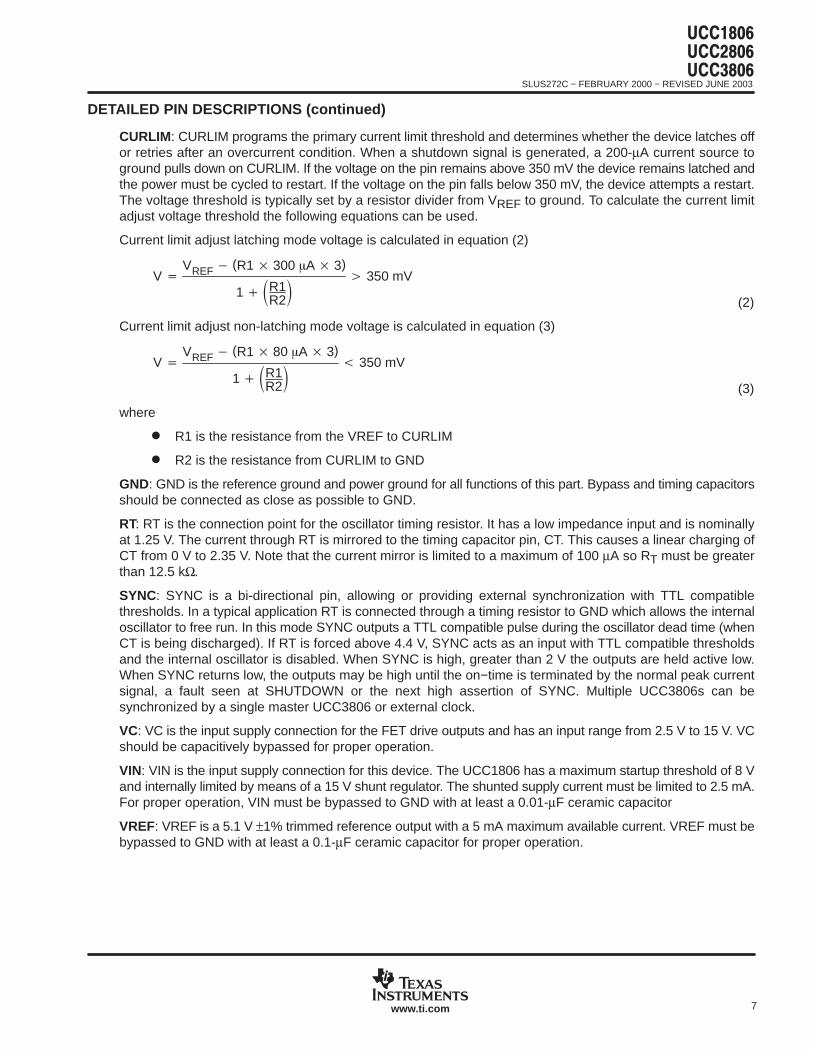
CURLIM: CURLIM programs the primary current limit threshold and determines whether the device latches offor retries after an overcurrent condition. When a shutdown signal is generated, a 200-µA current source toground pulls down on CURLIM. If the voltage on the pin remains above 350 mV the device remains latched andthe power must be cycled to restart. If the voltage on the pin falls below 350 mV, the device attempts a restart.The voltage threshold is typically set by a resistor divider from VREF to ground. To calculate the current limitadjust voltage threshold the following equations can be used.
Current limit adjust latching mode voltage is calculated in equation (2)
V
VREF (R1 300 A 3)
1 R1R2
350 mV
Current limit adjust non-latching mode voltage is calculated in equation (3)
V
VREF (R1 80 A 3)
1 R1R2
350 mV
where
R1 is the resistance from the VREF to CURLIM
R2 is the resistance from CURLIM to GND
GND: GND is the reference ground and power ground for all functions of this part. Bypass and timing capacitorsshould be connected as close as possible to GND.
RT: RT is the connection point for the oscillator timing resistor. It has a low impedance input and is nominallyat 1.25 V. The current through RT is mirrored to the timing capacitor pin, CT. This causes a linear charging ofCT from 0 V to 2.35 V. Note that the current mirror is limited to a maximum of 100 µA so RT must be greaterthan 12.5 kΩ.
SYNC: SYNC is a bi-directional pin, allowing or providing external synchronization with TTL compatiblethresholds. In a typical application RT is connected through a timing resistor to GND which allows the internaloscillator to free run. In this mode SYNC outputs a TTL compatible pulse during the oscillator dead time (whenCT is being discharged). If RT is forced above 4.4 V, SYNC acts as an input with TTL compatible thresholdsand the internal oscillator is disabled. When SYNC is high, greater than 2 V the outputs are held active low.When SYNC returns low, the outputs may be high until the on−time is terminated by the normal peak currentsignal, a fault seen at SHUTDOWN or the next high assertion of SYNC. Multiple UCC3806s can besynchronized by a single master UCC3806 or external clock.
VC: VC is the input supply connection for the FET drive outputs and has an input range from 2.5 V to 15 V. VCshould be capacitively bypassed for proper operation.
VIN: VIN is the input supply connection for this device. The UCC1806 has a maximum startup threshold of 8 Vand internally limited by means of a 15 V shunt regulator. The shunted supply current must be limited to 2.5 mA.For proper operation, VIN must be bypassed to GND with at least a 0.01-µF ceramic capacitor
VREF: VREF is a 5.1 V ±1% trimmed reference output with a 5 mA maximum available current. VREF must bebypassed to GND with at least a 0.1-µF ceramic capacitor for proper operation.
(2)
(3)
SLUS272C − FEBRUARY 2000 − REVISED JUNE 2003
8 www.ti.com
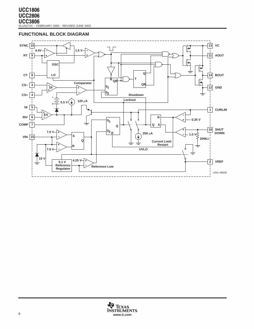
FUNCTIONAL BLOCK DIAGRAM
UDG−99035
10
7
3
8
SYNC
9RT +
−4.4V
+
−1.5 V
OSC
LOCT
+
−3X
4
+−
5
+
−EA
6
1
S1
QBR
S2
13 VC
11 AOUT
14 BOUT
12 GND
T
Q
QB
Shutdown
Lockout
S1Q
RS2
+−
+
−
16
1.0 V
0.35 V
Q
R
S
Current LimitRestart
UVLO
15
+
−
+
−
15 V5.1 V
ReferenceRegulator
+− Reference Low
4.25 V 2
CURLIM
SHUT
VREF
0.5 V
−
+
Comparator
7.0 V
7.5 V
CS−
CS+
NI
INV
COMP
VIN
SQ
R
200kΩ
200 µA
120 µA
DOWN
SLUS272C − FEBRUARY 2000 − REVISED JUNE 2003
9www.ti.com
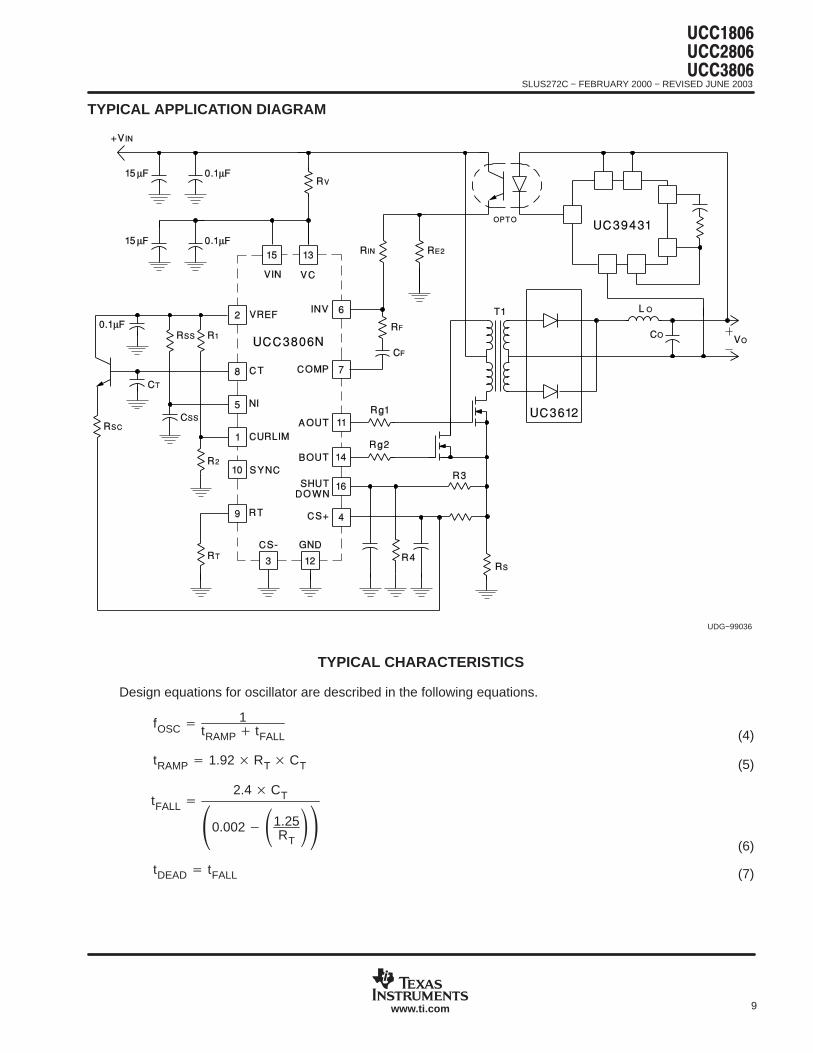
TYPICAL APPLICATION DIAGRAM
UDG−99036
TYPICAL CHARACTERISTICS
Design equations for oscillator are described in the following equations.
fOSC 1
tRAMP tFALL
tRAMP 1.92 RT CT
tFALL
2.4 CT
0.002 1.25RT
tDEAD tFALL
(4)
(5)
(6)
(7)
SLUS272C − FEBRUARY 2000 − REVISED JUNE 2003
10 www.ti.com
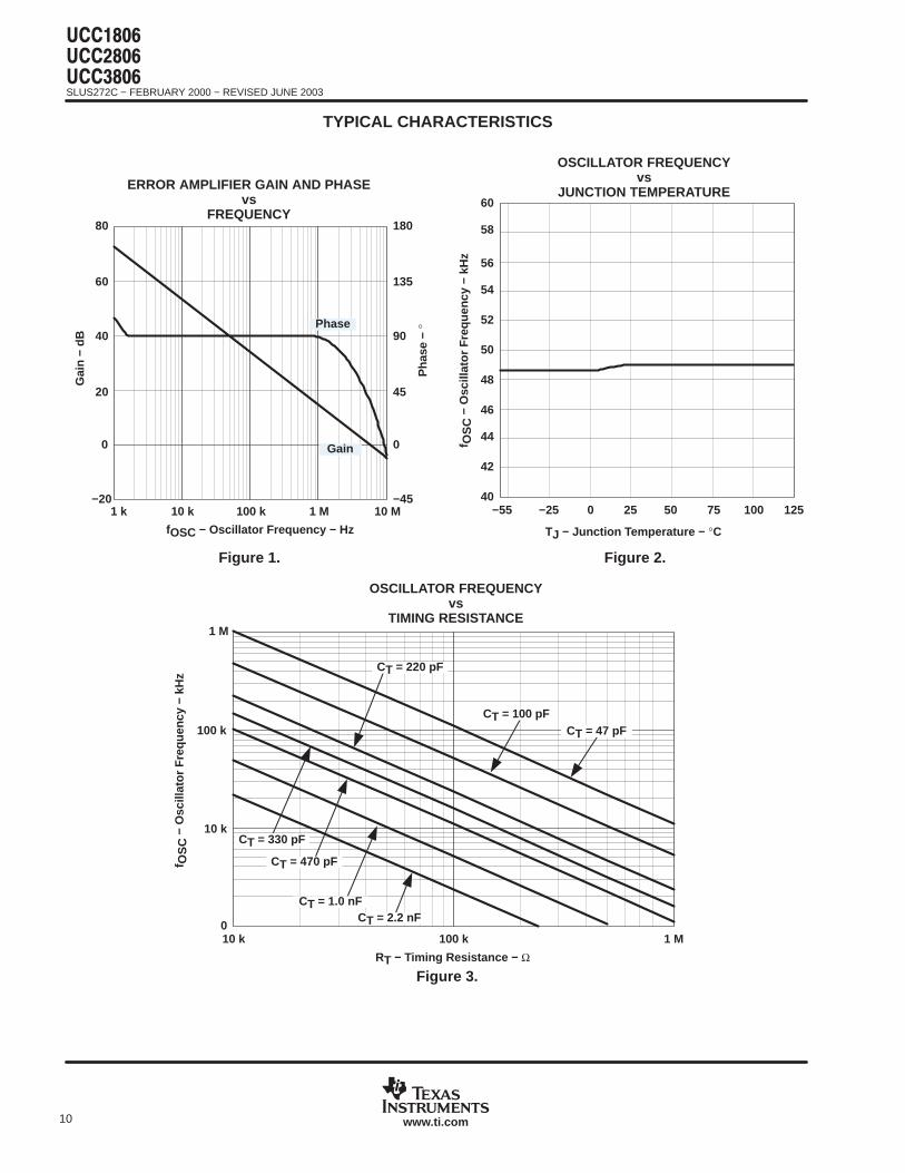
TYPICAL CHARACTERISTICS
Figure 1.
1 k
40
−2010 k
20
0
60
80
90
−45
45
0
135
180
100 k 1 M 10 M
ERROR AMPLIFIER GAIN AND PHASEvs
FREQUENCY
fOSC − Oscillator Frequency − Hz
Gai
n −
dB
Pha
se −
°
Gain
Phase
Figure 2.
52
40
44
42
54
46
50
48
56
58
60
−55 −25 0 25 50 75 100 125
TJ − Junction Temperature − °C
OSCILLATOR FREQUENCYvs
JUNCTION TEMPERATURE
f OS
C −
Osc
illat
or F
requ
ency
− k
Hz
10 k0
100 k 1 M
10 k
100 k
1 M
CT = 47 pFCT = 100 pF
f OS
C −
Osc
illat
or F
requ
ency
− k
Hz
RT − Timing Resistance − Ω
CT = 220 pF
CT = 2.2 nFCT = 1.0 nF
CT = 470 pF
CT = 330 pF
Figure 3.
OSCILLATOR FREQUENCYvs
TIMING RESISTANCE
PACKAGING INFORMATION
Orderable Device Status (1) PackageType
PackageDrawing
Pins PackageQty
Eco Plan (2) Lead/Ball Finish MSL Peak Temp (3)
5962-9457501MEA ACTIVE CDIP J 16 1 None A42 SNPB Level-NC-NC-NC
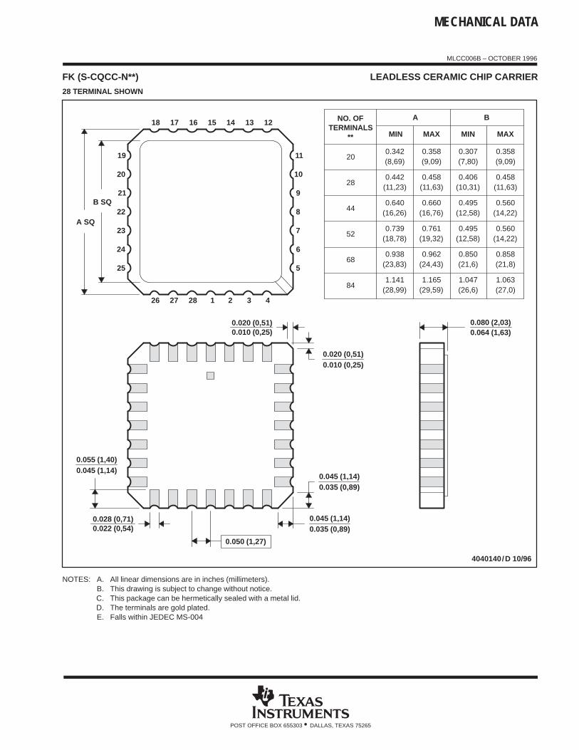
5962-9457501Q2A ACTIVE LCCC FK 20 1 None POST-PLATE Level-NC-NC-NC
5962-9457501V2A ACTIVE LCCC FK 20 1 None Call TI Level-NC-NC-NC
5962-9457501VEA ACTIVE CDIP J 16 1 None Call TI Level-NC-NC-NC
UCC1806J ACTIVE CDIP J 16 1 None A42 SNPB Level-NC-NC-NC
UCC1806J883B ACTIVE CDIP J 16 1 None A42 SNPB Level-NC-NC-NC
UCC1806JQMLV ACTIVE CDIP J 16 None Call TI Call TI
UCC1806L ACTIVE LCCC FK 20 1 None POST-PLATE Level-NC-NC-NC
UCC1806L883B ACTIVE LCCC FK 20 1 None POST-PLATE Level-NC-NC-NC
UCC1806LQMLV ACTIVE LCCC FK 20 None Call TI Call TI
UCC2806D ACTIVE SOIC D 16 40 None CU NIPDAU Level-1-220C-UNLIM
UCC2806DTR ACTIVE SOIC D 16 2500 None CU NIPDAU Level-1-220C-UNLIM
UCC2806DW ACTIVE SOIC DW 16 40 None CU NIPDAU Level-2-220C-1 YEAR
UCC2806DWTR ACTIVE SOIC DW 16 2000 None CU NIPDAU Level-2-220C-1 YEAR
UCC2806J ACTIVE CDIP J 16 1 None A42 SNPB Level-NC-NC-NC
UCC2806M ACTIVE SSOP/QSOP
DBQ 16 75 None CU NIPDAU Level-2-220C-1 YEAR
UCC2806MTR ACTIVE SSOP/QSOP
DBQ 16 2500 None CU NIPDAU Level-2-220C-1 YEAR
UCC2806N ACTIVE PDIP N 16 25 None CU SNPB Level-NA-NA-NA
UCC2806PW ACTIVE TSSOP PW 16 90 None CU NIPDAU Level-2-220C-1 YEAR
UCC2806PWTR ACTIVE TSSOP PW 16 2000 None CU NIPDAU Level-2-220C-1 YEAR
UCC2806PWTRG4 ACTIVE TSSOP PW 16 2000 Green (RoHS &no Sb/Br)
CU NIPDAU Level-1-260C-UNLIM
UCC2806Q ACTIVE PLCC FN 20 46 None CU SNPB Level-2-220C-1 YEAR
UCC2806QTR ACTIVE PLCC FN 20 1000 None CU SNPB Level-2-220C-1 YEAR
UCC3806DW ACTIVE SOIC DW 16 40 None CU NIPDAU Level-2-220C-1 YEAR
UCC3806DWTR ACTIVE SOIC DW 16 2000 None CU NIPDAU Level-2-220C-1 YEAR
UCC3806J ACTIVE CDIP J 16 1 None A42 SNPB Level-NC-NC-NC
UCC3806N ACTIVE PDIP N 16 25 None CU SNPB Level-NA-NA-NA
UCC3806PW ACTIVE TSSOP PW 16 90 None CU NIPDAU Level-2-220C-1 YEAR
UCC3806PWTR ACTIVE TSSOP PW 16 2000 None CU NIPDAU Level-2-220C-1 YEAR
UCC3806Q ACTIVE PLCC FN 20 46 None CU SNPB Level-2-220C-1 YEAR
UCC3806QTR ACTIVE PLCC FN 20 1000 None CU SNPB Level-2-220C-1 YEAR
(1) The marketing status values are defined as follows:ACTIVE: Product device recommended for new designs.LIFEBUY: TI has announced that the device will be discontinued, and a lifetime-buy period is in effect.NRND: Not recommended for new designs. Device is in production to support existing customers, but TI does not recommend using this part ina new design.PREVIEW: Device has been announced but is not in production. Samples may or may not be available.OBSOLETE: TI has discontinued the production of the device.
(2) Eco Plan - May not be currently available - please check http://www.ti.com/productcontent for the latest availability information and additionalproduct content details.None: Not yet available Lead (Pb-Free).
PACKAGE OPTION ADDENDUM
www.ti.com 8-Mar-2005
Addendum-Page 1
Pb-Free (RoHS): TI's terms "Lead-Free" or "Pb-Free" mean semiconductor products that are compatible with the current RoHS requirementsfor all 6 substances, including the requirement that lead not exceed 0.1% by weight in homogeneous materials. Where designed to be solderedat high temperatures, TI Pb-Free products are suitable for use in specified lead-free processes.Green (RoHS & no Sb/Br): TI defines "Green" to mean "Pb-Free" and in addition, uses package materials that do not contain halogens,including bromine (Br) or antimony (Sb) above 0.1% of total product weight.
(3) MSL, Peak Temp. -- The Moisture Sensitivity Level rating according to the JEDECindustry standard classifications, and peak soldertemperature.
Important Information and Disclaimer:The information provided on this page represents TI's knowledge and belief as of the date that it isprovided. TI bases its knowledge and belief on information provided by third parties, and makes no representation or warranty as to theaccuracy of such information. Efforts are underway to better integrate information from third parties. TI has taken and continues to takereasonable steps to provide representative and accurate information but may not have conducted destructive testing or chemical analysis onincoming materials and chemicals. TI and TI suppliers consider certain information to be proprietary, and thus CAS numbers and other limitedinformation may not be available for release.
In no event shall TI's liability arising out of such information exceed the total purchase price of the TI part(s) at issue in this document sold by TIto Customer on an annual basis.
PACKAGE OPTION ADDENDUM
www.ti.com 8-Mar-2005
Addendum-Page 2
MECHANICAL DATA
MLCC006B – OCTOBER 1996
POST OFFICE BOX 655303 • DALLAS, TEXAS 75265
FK (S-CQCC-N**) LEADLESS CERAMIC CHIP CARRIER
4040140/D 10/96
28 TERMINAL SHOWN
B
0.358(9,09)
MAX
(11,63)
0.560(14,22)
0.560
0.458
0.858(21,8)
1.063(27,0)
(14,22)
ANO. OF
MINMAX
0.358
0.660
0.761
0.458
0.342(8,69)
MIN
(11,23)
(16,26)0.640
0.739
0.442
(9,09)
(11,63)
(16,76)
0.962
1.165
(23,83)0.938
(28,99)1.141
(24,43)
(29,59)
(19,32)(18,78)
**
20
28
52
44
68
84
0.020 (0,51)
TERMINALS
0.080 (2,03)0.064 (1,63)
(7,80)0.307
(10,31)0.406
(12,58)0.495
(12,58)0.495
(21,6)0.850
(26,6)1.047
0.045 (1,14)
0.045 (1,14)0.035 (0,89)
0.035 (0,89)
0.010 (0,25)
121314151618 17
11
10
8
9
7
5
432
0.020 (0,51)0.010 (0,25)
6
12826 27
19
21B SQ
A SQ22
23
24
25
20
0.055 (1,40)0.045 (1,14)
0.028 (0,71)0.022 (0,54)
0.050 (1,27)
NOTES: A. All linear dimensions are in inches (millimeters).B. This drawing is subject to change without notice.C. This package can be hermetically sealed with a metal lid.D. The terminals are gold plated.E. Falls within JEDEC MS-004
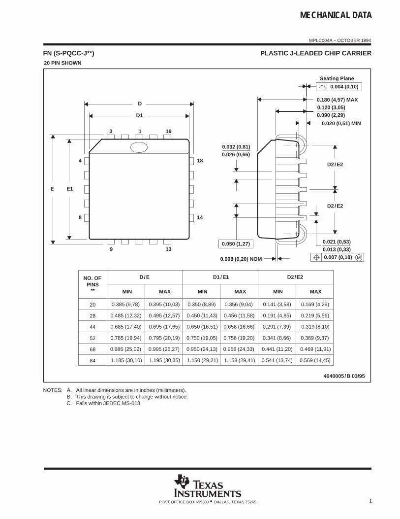
MECHANICAL DATA
MPLC004A – OCTOBER 1994
1POST OFFICE BOX 655303 • DALLAS, TEXAS 75265
FN (S-PQCC-J**) PLASTIC J-LEADED CHIP CARRIER
4040005/B 03/95
20 PIN SHOWN
0.026 (0,66)0.032 (0,81)
D2/E2
0.020 (0,51) MIN
0.180 (4,57) MAX0.120 (3,05)0.090 (2,29)
D2/E2
0.013 (0,33)0.021 (0,53)
Seating Plane
MAX
D2/E2
0.219 (5,56)
0.169 (4,29)
0.319 (8,10)
0.469 (11,91)
0.569 (14,45)
0.369 (9,37)
MAX
0.356 (9,04)
0.456 (11,58)
0.656 (16,66)
0.008 (0,20) NOM
1.158 (29,41)
0.958 (24,33)
0.756 (19,20)
0.191 (4,85)
0.141 (3,58)
MIN
0.441 (11,20)
0.541 (13,74)
0.291 (7,39)
0.341 (8,66)
18
19
14
13
D
D1
13
9
E1E
4
8
MINMAXMINPINS
**
20
28
44
0.385 (9,78)
0.485 (12,32)
0.685 (17,40)
52
68
84 1.185 (30,10)
0.985 (25,02)
0.785 (19,94)
D/E
0.395 (10,03)
0.495 (12,57)
1.195 (30,35)
0.995 (25,27)
0.695 (17,65)
0.795 (20,19)
NO. OF D1/E1
0.350 (8,89)
0.450 (11,43)
1.150 (29,21)
0.950 (24,13)
0.650 (16,51)
0.750 (19,05)
0.004 (0,10)
M0.007 (0,18)
0.050 (1,27)
NOTES: A. All linear dimensions are in inches (millimeters).B. This drawing is subject to change without notice.C. Falls within JEDEC MS-018
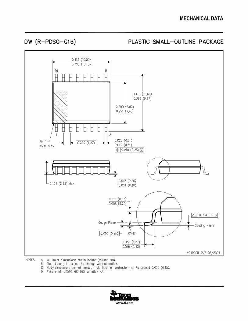
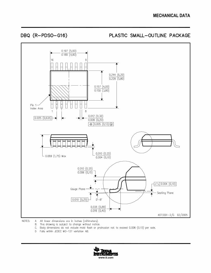
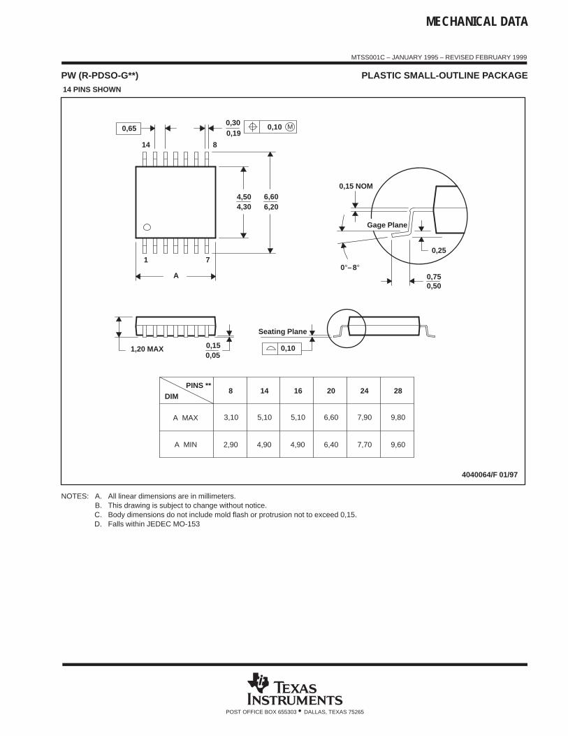
MECHANICAL DATA
MTSS001C – JANUARY 1995 – REVISED FEBRUARY 1999
POST OFFICE BOX 655303 • DALLAS, TEXAS 75265
PW (R-PDSO-G**) PLASTIC SMALL-OUTLINE PACKAGE14 PINS SHOWN
0,65 M0,10
0,10
0,25
0,500,75
0,15 NOM
Gage Plane
28
9,80
9,60
24
7,90
7,70
2016
6,60
6,40
4040064/F 01/97
0,30
6,606,20
8
0,19
4,304,50
7
0,15
14
A
1
1,20 MAX
14
5,10
4,90
8
3,10
2,90
A MAX
A MIN
DIMPINS **
0,05
4,90
5,10
Seating Plane
0°–8°
NOTES: A. All linear dimensions are in millimeters.B. This drawing is subject to change without notice.C. Body dimensions do not include mold flash or protrusion not to exceed 0,15.D. Falls within JEDEC MO-153
IMPORTANT NOTICE
Texas Instruments Incorporated and its subsidiaries (TI) reserve the right to make corrections, modifications,enhancements, improvements, and other changes to its products and services at any time and to discontinueany product or service without notice. Customers should obtain the latest relevant information before placingorders and should verify that such information is current and complete. All products are sold subject to TI’s termsand conditions of sale supplied at the time of order acknowledgment.
TI warrants performance of its hardware products to the specifications applicable at the time of sale inaccordance with TI’s standard warranty. Testing and other quality control techniques are used to the extent TIdeems necessary to support this warranty. Except where mandated by government requirements, testing of allparameters of each product is not necessarily performed.
TI assumes no liability for applications assistance or customer product design. Customers are responsible fortheir products and applications using TI components. To minimize the risks associated with customer productsand applications, customers should provide adequate design and operating safeguards.
TI does not warrant or represent that any license, either express or implied, is granted under any TI patent right,copyright, mask work right, or other TI intellectual property right relating to any combination, machine, or processin which TI products or services are used. Information published by TI regarding third-party products or servicesdoes not constitute a license from TI to use such products or services or a warranty or endorsement thereof.Use of such information may require a license from a third party under the patents or other intellectual propertyof the third party, or a license from TI under the patents or other intellectual property of TI.
Reproduction of information in TI data books or data sheets is permissible only if reproduction is withoutalteration and is accompanied by all associated warranties, conditions, limitations, and notices. Reproductionof this information with alteration is an unfair and deceptive business practice. TI is not responsible or liable forsuch altered documentation.
Resale of TI products or services with statements different from or beyond the parameters stated by TI for thatproduct or service voids all express and any implied warranties for the associated TI product or service andis an unfair and deceptive business practice. TI is not responsible or liable for any such statements.
Following are URLs where you can obtain information on other Texas Instruments products and applicationsolutions:
Products Applications
Amplifiers amplifier.ti.com Audio www.ti.com/audio
Data Converters dataconverter.ti.com Automotive www.ti.com/automotive
DSP dsp.ti.com Broadband www.ti.com/broadband
Interface interface.ti.com Digital Control www.ti.com/digitalcontrol
Logic logic.ti.com Military www.ti.com/military
Power Mgmt power.ti.com Optical Networking www.ti.com/opticalnetwork
Microcontrollers microcontroller.ti.com Security www.ti.com/security
Telephony www.ti.com/telephony
Video & Imaging www.ti.com/video
Wireless www.ti.com/wireless
Mailing Address: Texas Instruments
Post Office Box 655303 Dallas, Texas 75265
Copyright 2005, Texas Instruments Incorporated