Embed Size (px)
Citation preview
January 2007
LM4949
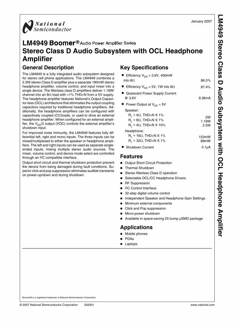
Stereo Class D Audio Subsystem with OCL HeadphoneAmplifierGeneral DescriptionThe LM4949 is a fully integrated audio subsystem designedfor stereo cell phone applications. The LM4949 combines a2.5W stereo Class D amplifier plus a separate 190mW stereoheadphone amplifier, volume control, and input mixer into asingle device. The filterless class D amplifiers deliver 1.19W/channel into an 8Ω load with <1% THD+N from a 5V supply.The headphone amplifier features National’s Output Capaci-tor-less (OCL) architecture that eliminates the output couplingcapacitors required by traditional headphone amplifiers. Ad-ditionally, the headphone amplifiers can be configured withcapacitively coupled (CC)loads, or used to drive an externalheadphone amplifier. When configured for an external ampli-fier, the VDD/2 output (VOC) controls the external amplifier’sshutdown input.
For improved noise immunity, the LM4949 features fully dif-ferential left, right and mono inputs. The three inputs can bemixed/multiplexed to either the speaker or headphone ampli-fiers. The left and right inputs can be used as separate single-ended inputs, mixing multiple stereo audio sources. Themixer, volume control, and device mode select are controlledthrough an I2C compatible interface.
Output short circuit and thermal shutdown protection preventthe device from being damaged during fault conditions. Su-perior click and pop suppression eliminates audible transientson power-up/down and during shutdown.
Key Specifications
Efficiency VDD = 3.6V, 400mW
into 8Ω 86.5%
Efficiency VDD = 5V, 1W into 8Ω 87.4%
Quiescent Power Supply Current
@ 3.6V 9.36mA
Power Output at VDD = 5V
Speaker:
RL = 4Ω, THD+N ≤ 1%
RL = 8Ω, THD+N ≤ 1%
RL = 4Ω, THD+N ≤ 10%
2W1.19W
2.5W
Headphone:
RL = 16Ω, THD+N ≤ 1%
RL = 32Ω, THD+N ≤ 1%153mW
89mW
Shutdown Current 0.1μA
Features Output Short Circuit Protection
Thermal Shutdown
Stereo filterless Class D operation
Selectable OCL/CC Headphone Drivers
RF Suppression
I2C Control Interface
32-step digital volume control
Independent Speaker and Headphone Gain Settings
Minimum external components
Click and Pop suppression
Micro-power shutdown
Available in space-saving 25 bump µSMD package
Applications Mobile phones
PDAs
Laptops
Boomer® is a registered trademark of National Semiconductor Corporation.
© 2007 National Semiconductor Corporation 202001 www.national.com
LM
4949 S
tere
o C
lass D
Au
dio
Su
bsyste
m w
ith O
CL
Head
ph
on
e A
mp
lifier
Typical Application
202001c6
FIGURE 1. Typical Audio Amplifier Application Circuit
www.national.com 2
LM
4949
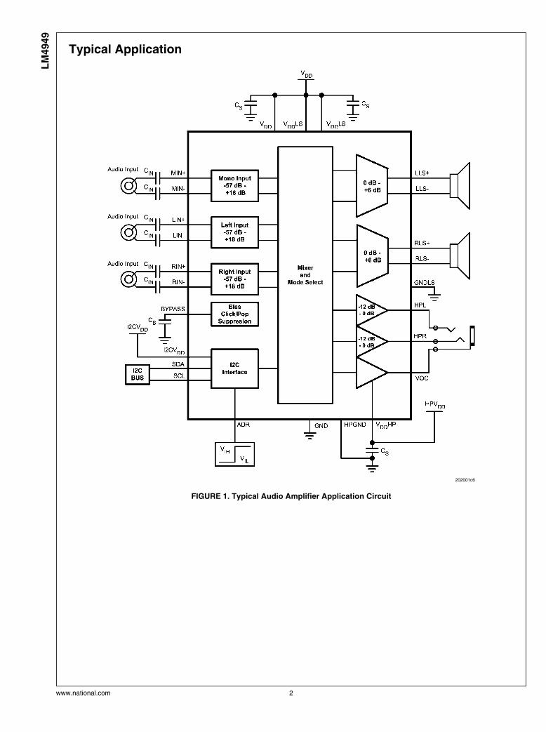
Connection Diagrams
TL Package2.68mm x 2.68mm x 0.6mm
202001c7
Top ViewOrder Number LM4949TL
See NS Package Number TLA25JJA
LM4949TL Marking
202001c0
Top ViewXY — 2 digit datecodeTT — Die traceability
3 www.national.com
LM
4949
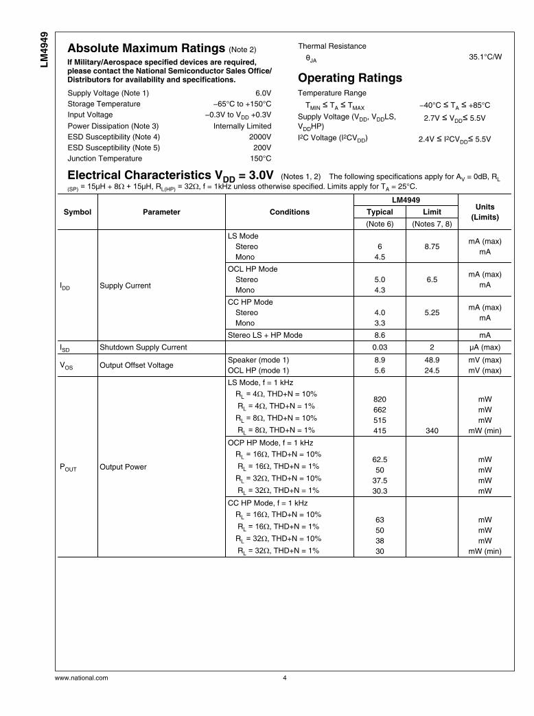
Absolute Maximum Ratings (Note 2)
If Military/Aerospace specified devices are required,please contact the National Semiconductor Sales Office/Distributors for availability and specifications.
Supply Voltage (Note 1) 6.0V
Storage Temperature −65°C to +150°C
Input Voltage −0.3V to VDD +0.3V
Power Dissipation (Note 3) Internally Limited
ESD Susceptibility (Note 4) 2000V
ESD Susceptibility (Note 5) 200V
Junction Temperature 150°C
Thermal Resistance
θJA35.1°C/W
Operating RatingsTemperature Range
TMIN ≤ TA ≤ TMAX −40°C ≤ TA ≤ +85°C
Supply Voltage (VDD, VDDLS,VDDHP)
2.7V ≤ VDD≤ 5.5V
I2C Voltage (I2CVDD) 2.4V ≤ I2CVDD≤ 5.5V
Electrical Characteristics VDD = 3.0V (Notes 1, 2) The following specifications apply for AV = 0dB, RL
(SP) = 15μH + 8Ω + 15μH, RL(HP) = 32Ω, f = 1kHz unless otherwise specified. Limits apply for TA = 25°C.
Symbol Parameter Conditions
LM4949Units
(Limits)Typical Limit
(Note 6) (Notes 7, 8)
IDD Supply Current
LS Mode
Stereo
Mono
6
4.5
8.75mA (max)
mA
OCL HP Mode
Stereo
Mono
5.0
4.3
6.5mA (max)
mA
CC HP Mode
Stereo
Mono
4.0
3.3
5.25mA (max)
mA
Stereo LS + HP Mode 8.6 mA
ISD Shutdown Supply Current 0.03 2 µA (max)
VOS Output Offset VoltageSpeaker (mode 1)
OCL HP (mode 1)
8.9
5.6
48.9
24.5
mV (max)
mV (max)
POUT Output Power
LS Mode, f = 1 kHz
RL = 4Ω, THD+N = 10%
RL = 4Ω, THD+N = 1%
RL = 8Ω, THD+N = 10%
RL = 8Ω, THD+N = 1%
820
662
515
415 340
mW
mW
mW
mW (min)
OCP HP Mode, f = 1 kHz
RL = 16Ω, THD+N = 10%
RL = 16Ω, THD+N = 1%
RL = 32Ω, THD+N = 10%
RL = 32Ω, THD+N = 1%
62.5
50
37.5
30.3
mW
mW
mW
mW
CC HP Mode, f = 1 kHz
RL = 16Ω, THD+N = 10%
RL = 16Ω, THD+N = 1%
RL = 32Ω, THD+N = 10%
RL = 32Ω, THD+N = 1%
63
50
38
30
mW
mW
mW
mW (min)
www.national.com 4
LM
4949
Symbol Parameter Conditions
LM4949Units
(Limits)Typical Limit
(Note 6) (Notes 7, 8)
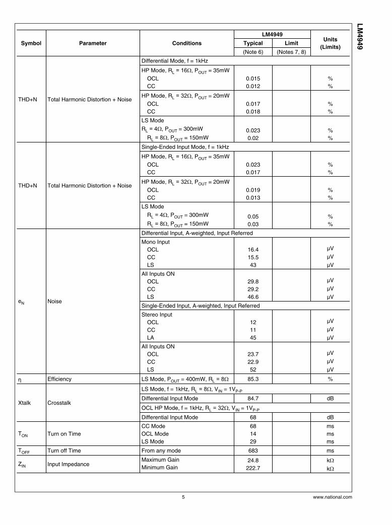
THD+N Total Harmonic Distortion + Noise
Differential Mode, f = 1kHz
HP Mode, RL = 16Ω, POUT = 35mW
OCL
CC
0.015
0.012
%
%
HP Mode, RL = 32Ω, POUT = 20mW
OCL
CC
0.017
0.018
%
%
LS Mode
RL = 4Ω, POUT = 300mW
RL = 8Ω, POUT = 150mW
0.023
0.02
%
%
THD+N Total Harmonic Distortion + Noise
Single-Ended Input Mode, f = 1kHz
HP Mode, RL = 16Ω, POUT = 35mW
OCL
CC
0.023
0.017
%
%
HP Mode, RL = 32Ω, POUT = 20mW
OCL
CC
0.019
0.013
%
%
LS Mode
RL = 4Ω, POUT = 300mW
RL = 8Ω, POUT = 150mW
0.05
0.03
%
%
eN Noise
Differential Input, A-weighted, Input Referred
Mono Input
OCL
CC
LS
16.4
15.5
43
μV
μV
μV
All Inputs ON
OCL
CC
LS
29.8
29.2
46.6
μV
μV
μV
Single-Ended Input, A-weighted, Input Referred
Stereo Input
OCL
CC
LA
12
11
45
μV
μV
μV
All Inputs ON
OCL
CC
LS
23.7
22.9
52
μV
μV
μV
η Efficiency LS Mode, POUT = 400mW, RL = 8Ω 85.3 %
Xtalk Crosstalk
LS Mode, f = 1kHz, RL = 8Ω, VIN = 1VP-P
Differential Input Mode 84.7 dB
OCL HP Mode, f = 1kHz, RL = 32Ω, VIN = 1VP-P
Differential Input Mode 68 dB
TON Turn on Time
CC Mode
OCL Mode
LS Mode
68
14
29
ms
ms
ms
TOFF Turn off Time From any mode 683 ms
ZIN Input ImpedanceMaximum Gain
Minimum Gain24.8
222.7
kΩkΩ
5 www.national.com
LM
4949
Symbol Parameter Conditions
LM4949Units
(Limits)Typical Limit
(Note 6) (Notes 7, 8)
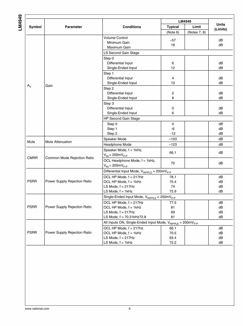
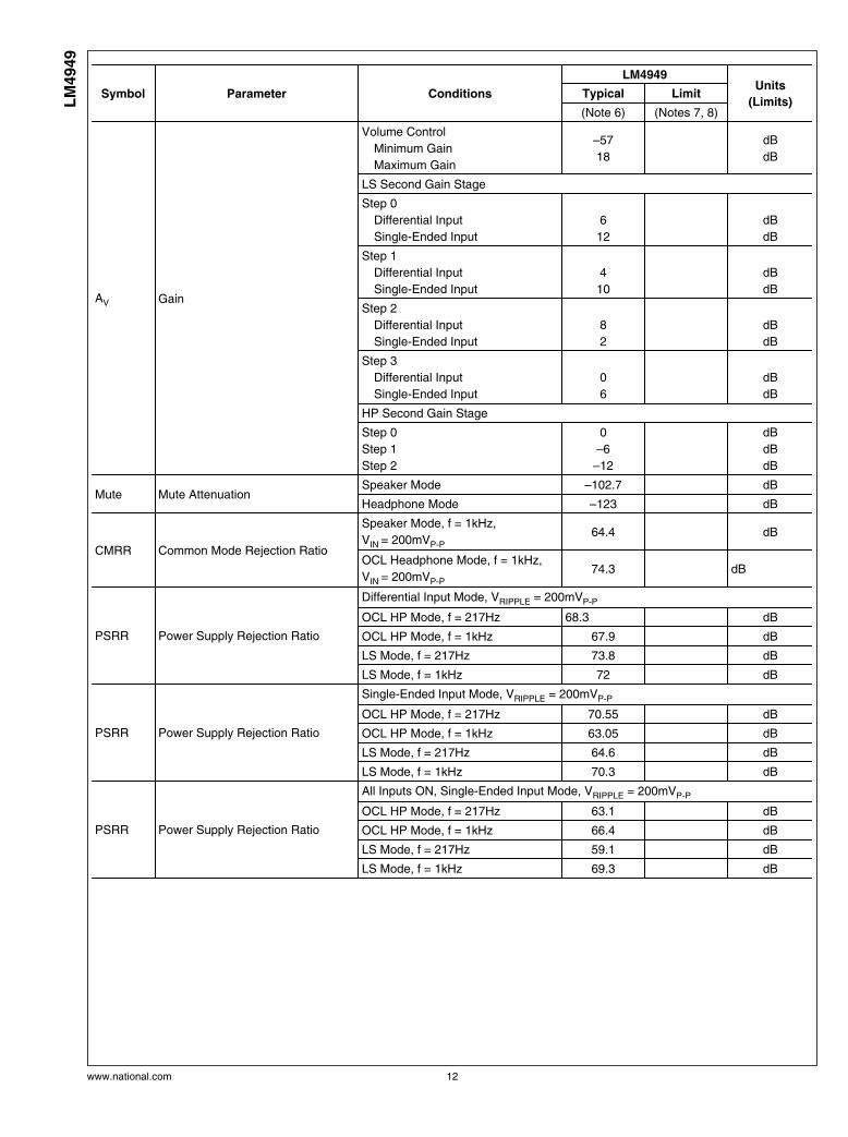
AV Gain
Volume Control
Minimum Gain
Maximum Gain
–57
18
dB
dB
LS Second Gain Stage
Step 0
Differential Input
Single-Ended Input
6
12
dB
dB
Step 1
Differential Input
Single-Ended Input
4
10
dB
dB
Step 2
Differential Input
Single-Ended Input
2
8
dB
dB
Step 3
Differential Input
Single-Ended Input
0
6
dB
dB
HP Second Gain Stage
Step 0
Step 1
Step 2
0
-6
-12
dB
dB
dB
Mute Mute AttenuationSpeaker Mode –103 dB
Headphone Mode –123 dB
CMRR Common Mode Rejection Ratio
Speaker Mode, f = 1kHz,
VIN = 200mVP-P
66.1
dB
OCL Headphone Mode, f = 1kHz,
VIN = 200mVP-P
70
dB
PSRR Power Supply Rejection Ratio
Differential Input Mode, VRIPPLE = 200mVP-P
OCL HP Mode, f = 217Hz
OCL HP Mode, f = 1kHz
LS Mode, f = 217Hz
LS Mode, f = 1kHz
78.1
75.4
74
72.9
dB
dB
dB
dB
PSRR Power Supply Rejection Ratio
Single-Ended Input Mode, VRIPPLE = 200mVP-P
OCL HP Mode, f = 217Hz
OCL HP Mode, f = 1kHz
LS Mode, f = 217Hz
LS Mode, f = 70.31kHz72.8
77.5
81
69
81
dB
dB
dB
dB
PSRR Power Supply Rejection Ratio
All Inputs ON, Single-Ended Input Mode, VRIPPLE = 200mVP-P
OCL HP Mode, f = 217Hz
OCL HP Mode, f = 1kHz
LS Mode, f = 217Hz
LS Mode, f = 1kHz
66.1
70.5
65.4
72.2
dB
dB
dB
dB
www.national.com 6
LM
4949
Electrical Characteristics VDD = 3.6V (Notes 1, 2) The following specifications apply for AV = 0dB, RL
(SP) = 15μH + 8Ω + 15μH, RL(HP) = 32Ω, f = 1kHz unless otherwise specified. Limits apply for TA = 25°C.
Symbol Parameter Conditions
LM4949Units
(Limits)Typical Limit
(Note 6) (Notes 7, 8)
IDD Supply Current
LS Mode
Stereo
Mono
6.8
4.9
7.3
5.3
mA (max)
mA (max)
OCL HP Mode
Stereo
Mono
5.8
4.9
6.5
5.5
mA (max)
mA (max)
CC HP Mode
Stereo
Mono
4.7
4.1
5.2
4.6
mA (max)
mA (max)
Stereo LS + HP Mode 9.36 mA
ISD Shutdown Supply Current 0.03 1 µA (max)
VOS Output Offset VoltageHeadphone
Speaker
6.7
8.9
20
49
mV (max)
mV (max)
POUT Output Power
LS Mode, f = 1 kHz
RL = 4Ω, THD+N = 10%
RL = 4Ω, THD+N = 1%
RL = 8Ω, THD+N = 10%
RL = 8Ω, THD+N = 1%
1.24
1
0.765
0.615
W
W
W
W
OCL HP Mode, f = 1 kHz
RL = 16Ω, THD+N = 10%
RL = 16Ω, THD+N = 1%
RL = 32Ω, THD+N = 10%
RL = 32Ω, THD+N = 1%
94
76
55
45
mW
mW
mW
mW
CC HP Mode, f = 1 kHz
RL = 16Ω, THD+N = 10%
RL = 16Ω, THD+N = 1%
RL = 32Ω, THD+N = 10%
RL = 32Ω, THD+N = 1%
93
75
56
45
mW
mW
mW
mW
THD+N Total Harmonic Distortion + Noise
Differential Mode, f = 1kHz
HP Mode, RL = 16Ω, POUT = 50mW
OCL
CC
0.021
0.021
%
%
HP Mode, RL = 32Ω,POUT = 30mW
OCL
CC
0.01
0.01
%
%
LS Mode
RL = 4Ω, POUT = 400mW
RL = 8Ω, POUT = 300mW
0.023
0.02
%
%
7 www.national.com
LM
4949
Symbol Parameter Conditions
LM4949Units
(Limits)Typical Limit
(Note 6) (Notes 7, 8)
THD+N Total Harmonic Distortion + Noise
Single-Ended Input Mode, f = 1kHz
HP Mode, RL = 16Ω, POUT = 50mW
OCL
CC
0.021
0.017
%
%
HP Mode, RL = 32Ω, POUT = 30mW
OCL
CC
0.02
0.015
%
%
LS Mode
RL = 4Ω, POUT = 400mW
RL = 8Ω, POUT = 300mW
0.05
0.034
%
%
eN Noise
Differential Mode, A-weighted, Input Referred
Mono Input
OCL
CC
LS
16.4
15.5
43
μV
μV
μV
All Inputs ON
OCL
CC
LS
29.8
29.2
46.6
μV
μV
μV
Single-Ended Input, A-weighted, Input Referred
Stereo Input
OCL
CC
LS
12
11
45
μV
μV
μV
All Inputs ON
OCL
CC
LS
23.7
22.9
52
μV
μV
μV
η Efficiency LS Mode, POUT = 400mW, RL = 8Ω 86.5 %
Xtalk Crosstalk
LS Mode, f = 1kHz, RL = 8Ω, VIN = 1VP-P
Differential Input Mode 86 dB
OCL HP Mode, f = 1kHz, RL = 32Ω, VIN = 1VP-P
Differential Input Mode 68 dB
TON Turn on Time
CC Mode
OCL Mode
LS Mode
75
14
31
ms
ms
TOFF Turn off Time From any mode 692 ms
ZIN Input ImpedanceMaximum Gain
Minimum Gain24.8
222.7
kΩkΩ
www.national.com 8
LM
4949
Symbol Parameter Conditions
LM4949Units
(Limits)Typical Limit
(Note 6) (Notes 7, 8)
AV Gain
Volume Control
Minimum Gain
Maximum Gain
–57
18
dB
dB
LS Second Gain Stage
Step 0
Differential Input
Single-Ended Input
6
12
dB
dB
Step 2
Differential Input
Single-Ended Input
4
10
dB
dB
Step 2
Differential Input
Single-Ended Input
2
8
dB
dB
Step 3
Differential Input
Single-Ended Input
0
6
dB
dB
HP Second Gain Stage
Step 0
Step 1
Step 2
0
–6
–12
dB
dB
Mute Mute AttenuationSpeaker Mode –84 dB
Headphone Mode –95 dB
CMRR Common Mode Rejection Ratio
Speaker Mode, f = 1kHz,
VIN = 200mVP-P
66
dB
OCL Headphone Mode, f = 1kHz,
VIN = 200mVP-P
68.6
dB
PSRR Power Supply Rejection Ratio
Differential Input Mode, VRIPPLE = 200mVP-P
OCL HP Mode, f = 217Hz
OCL HP Mode, f = 1kHz
LS Mode, f = 217Hz
LS Mode, f = 1kHz
75
75
73
73
dB
dB
dB
dB
PSRR Power Supply Rejection Ratio
Single-Ended Input Mode, VRIPPLE = 200mVP-P
OCL HP Mode, f = 217Hz
OCL HP Mode, f = 1kHz
LS Mode, f = 217Hz
LS Mode, f = 1kHz
75
75
67
71
dB
dB
dB
dB
PSRR Power Supply Rejection Ratio
All Inputs ON, Single-Ended Input Mode, VRIPPLE = 200mVP-P
OCL HP Mode, f = 217Hz
OCL HP Mode, f = 1kHz
LS Mode, f = 217Hz
LS Mode, f = 1kHz
72
70
60
65
dB
dB
dB
dB
9 www.national.com
LM
4949
Electrical Characteristics VDD = 5.0V (Notes 1, 2) The following specifications apply for AV = 0dB, RL
(SP) = 15μH + 8Ω + 15μH, RL(HP) = 32Ω, f = 1kHz unless otherwise specified. Limits apply for TA = 25°C.
Symbol Parameter Conditions
LM4949Units
(Limits)Typical Limit
(Note 6) (Notes 7, 8)
IDD Supply Current
LS Mode
Stereo
Mono
9.9
6.6
10.9
7.2
mA (max)
mA (max)
OCL HP Mode
Stereo
Mono
6.6
5.5
7.3
6.2
mA (max)
mA (max)
CC HP Mode
Stereo
Mono
5.4
4.3
5.9
4.8
mA (max)
mA (max)
Stereo LS + HP Mode 13 mA
ISD Shutdown Supply Current 0.1 1 µA (max)
VOS Output Offset VoltageHeadphone
Speaker
10
9.6
52
50
mV (max)
mV (max)
POUT Output Power
LS Mode, f = 1 kHz
RL = 4Ω, THD+N = 10%
RL = 4Ω, THD+N = 1%
RL = 8Ω, THD+N = 10%
RL = 8Ω, THD+N = 1%
2.5
2.01
1.48
1.19
W
W
W
W
OCL HP Mode, f = 1 kHz
RL = 16Ω, THD+N = 10%
RL = 16Ω, THD+N = 1%
RL = 32Ω, THD+N = 10%
RL = 32Ω, THD+N = 1%
190
154
109
89
mW
mW
mW
mW
CC HP Mode, f = 1 kHz
RL = 16Ω, THD+N = 10%
RL = 16Ω, THD+N = 1%
RL = 32Ω, THD+N = 10%
RL = 32Ω, THD+N = 1%
188
153
105
88
mW
mW
mW
mW
THD + N Total Harmonic Distortion + Noise
Differential Input Mode, f = 1kHz
HP Mode, RL = 16Ω, POUT = 100mW
OCL
CC
0.02
0.027
%
%
HP Mode, RL = 32Ω, POUT = 50mW
OCL
CC
0.02
0.022
%
%
LS Mode
RL = 4Ω, POUT = 1W
RL = 8Ω, POUT = 600mW
0.022
0.02
%
%
www.national.com 10
LM
4949
Symbol Parameter Conditions
LM4949Units
(Limits)Typical Limit
(Note 6) (Notes 7, 8)
THD + N Total Harmonic Distortion + Noise
Single-Ended Input Mode, f = 1kHz
HP Mode, RL = 16Ω, POUT = 100mW
OCL
CC
0.021
0.02
%
%
HP Mode, RL = 32Ω, POUT = 50mW
OCL
CC
0.02
0.017
%
%
LS Mode
RL = 4Ω, POUT = 1W
RL = 8Ω, POUT = 600mW
0.05
0.033
%
%
eN Noise
Differential Input, A-weighted, Input Referred
Mono Input
OCL
CC
LS
16.4
15.5
43
μV
μV
μV
All Inputs ON
OCL
CC
LS
29.8
29.2
46.6
μV
μV
μV
Single-Ended Input, A-weighted, Input Rrferred
Stereo Input
OCL
CC
LS
12
11
45
μV
μV
μV
All Inputs ON
OCL
CC
LS
23.7
22.9
52
μV
μV
μV
η Efficiency LS Mode, POUT = 1W, RL = 8Ω 87.4 %
Xtalk Crosstalk
LS Mode, f = 1kHz, RL = 8Ω, VIN = 1VP-P
Differential Input Mode 105.8 dB
OCL HP Mode, f = 1kHz, RL = 32Ω, VIN = 1VP-P
Differential Input Mode 69.6 dB
TON
Turn on Time
CC Mode
OCL Mode
LS Mode
89
14
35
ms
ms
ms
TOFF Turn off Time From any mode 716 ms
ZIN Input ImpedanceMaximum Gain
Minimum Gain24.8
222.7
kΩkΩ
11 www.national.com
LM
4949
Symbol Parameter Conditions
LM4949Units
(Limits)Typical Limit
(Note 6) (Notes 7, 8)
AV Gain
Volume Control
Minimum Gain
Maximum Gain
–57
18
dB
dB
LS Second Gain Stage
Step 0
Differential Input
Single-Ended Input
6
12
dB
dB
Step 1
Differential Input
Single-Ended Input
4
10
dB
dB
Step 2
Differential Input
Single-Ended Input
8
2
dB
dB
Step 3
Differential Input
Single-Ended Input
0
6
dB
dB
HP Second Gain Stage
Step 0
Step 1
Step 2
0
–6
–12
dB
dB
dB
Mute Mute AttenuationSpeaker Mode –102.7 dB
Headphone Mode –123 dB
CMRR Common Mode Rejection Ratio
Speaker Mode, f = 1kHz,
VIN = 200mVP-P
64.4
dB
OCL Headphone Mode, f = 1kHz,
VIN = 200mVP-P
74.3
dB
PSRR Power Supply Rejection Ratio
Differential Input Mode, VRIPPLE = 200mVP-P
OCL HP Mode, f = 217Hz 68.3 dB
OCL HP Mode, f = 1kHz 67.9 dB
LS Mode, f = 217Hz 73.8 dB
LS Mode, f = 1kHz 72 dB
PSRR Power Supply Rejection Ratio
Single-Ended Input Mode, VRIPPLE = 200mVP-P
OCL HP Mode, f = 217Hz 70.55 dB
OCL HP Mode, f = 1kHz 63.05 dB
LS Mode, f = 217Hz 64.6 dB
LS Mode, f = 1kHz 70.3 dB
PSRR Power Supply Rejection Ratio
All Inputs ON, Single-Ended Input Mode, VRIPPLE = 200mVP-P
OCL HP Mode, f = 217Hz 63.1 dB
OCL HP Mode, f = 1kHz 66.4 dB
LS Mode, f = 217Hz 59.1 dB
LS Mode, f = 1kHz 69.3 dB
www.national.com 12
LM
4949

Note 1: All voltages are measured with respect to the ground pin, unless otherwise specified.
Note 2: Absolute Maximum Ratings indicate limits beyond which damage to the device may occur. Operating Ratings indicate conditions for which the device isfunctional, but do not guarantee specific performance limits. Electrical Characteristics state DC and AC electrical specifications under particular test conditionswhich guarantee specific performance limits. This assumes that the device is within the Operating Ratings. Specifications are not guaranteed for parameterswhere no limit is given, however, the typical value is a good indication of device performance.
Note 3: The maximum power dissipation must be derated at elevated temperatures and is dictated by TJMAX, θJA, and the ambient temperature TA. The maximumallowable power dissipation is PDMAX = (TJMAX – TA) / θJA or the number given in Absolute Maximum Ratings, whichever is lower. For the LM4949, see powerderating currents for additional information.
Note 4: Human body model, 100pF discharged through a 1.5kΩ resistor.
Note 5: Machine Model, 220pF – 240pF discharged through all pins.
Note 6: Typicals are measured at 25°C and represent the parametric norm.
Note 7: Limits are guaranteed to National's AOQL (Average Outgoing Quality Level).
Note 8: Datasheet min/max specification limits are guaranteed by design, test or statistical analysis.
13 www.national.com
LM
4949

TABLE 1. Bump Description
BUMP NAME DESCRIPTION
A1 LLS- Left Channel Loudspeaker Inverting Output
A2 LLS+ Left Channel Loudspeaker Non-inverting Output
A3 SDA Serial Data Input
A4 HPGND Headphone Ground
A5 HPR Right Channel Headphone Output
B1 VDDLS Speaker Power Supply
B2 ADR Address Select Bit
B3 RIN- Right Channel Inverting Input
B4 HPL Left Channel Headphone Output
B5 VOC Headphone Return Bias Output
C1 GNDLS Speaker Ground
C2 VDD Power Supply
C3 RIN+ Right Channel Non-Inverting Input
C4 LIN+ Left Channel Non-inverting Input
C5 VDDHP Headphone Power Supply
D1 VDDLS Speaker Power Supply
D2 I2CVDD I2C Power Supply
D3 SCL Serial Clock Input
D4 MIN+ Mono Channel Non-inverting Input
D5 LIN- Left Channel Inverting Input
E1 RLS- Right Channel Loudspeaker Inverting Output
E2 RLS+ Right Channel Loudspeaker Non-inverting Output
E3 GND Ground
E4 MIN- Mono Channel Inverting Input
E5 BYPASS Mid-rail Bias Bypass
www.national.com 14
LM
4949
Typical Performance Characteristics
THD+N vs FrequencySpeaker Mode, Differential Input
VDD = 3.0V, POUT = 300mW, RL = 4Ω
202001f0
THD+N vs FrequencySpeaker Mode, Differential Input
VDD = 3.6V, POUT = 400mW, RL = 4Ω
202001f1
THD+N vs FrequencySpeaker Mode, Differential InputVDD = 5.0V, POUT = 1W, RL = 4Ω
202001f2
THD+N vs FrequencySpeaker Mode, Differential Input
VDD = 3.0V, POUT = 150mW, RL = 8Ω
202001f3
THD+N vs FrequencySpeaker Mode, Differential Input
VDD = 3.6V, POUT = 300mW, RL = 8Ω
202001f4
THD+N vs FrequencySpeaker Mode, Differential Input
VDD = 5.0V, POUT = 600mW, RL = 8Ω
202001f5
15 www.national.com
LM
4949
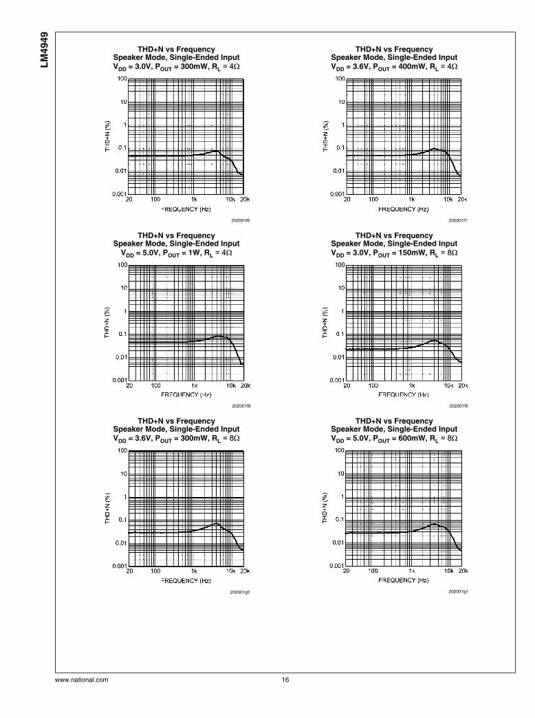
THD+N vs FrequencySpeaker Mode, Single-Ended InputVDD = 3.0V, POUT = 300mW, RL = 4Ω
202001f6
THD+N vs FrequencySpeaker Mode, Single-Ended InputVDD = 3.6V, POUT = 400mW, RL = 4Ω
202001f7
THD+N vs FrequencySpeaker Mode, Single-Ended Input
VDD = 5.0V, POUT = 1W, RL = 4Ω
202001f8
THD+N vs FrequencySpeaker Mode, Single-Ended InputVDD = 3.0V, POUT = 150mW, RL = 8Ω
202001f9
THD+N vs FrequencySpeaker Mode, Single-Ended InputVDD = 3.6V, POUT = 300mW, RL = 8Ω
202001g0
THD+N vs FrequencySpeaker Mode, Single-Ended InputVDD = 5.0V, POUT = 600mW, RL = 8Ω
202001g1
www.national.com 16
LM
4949
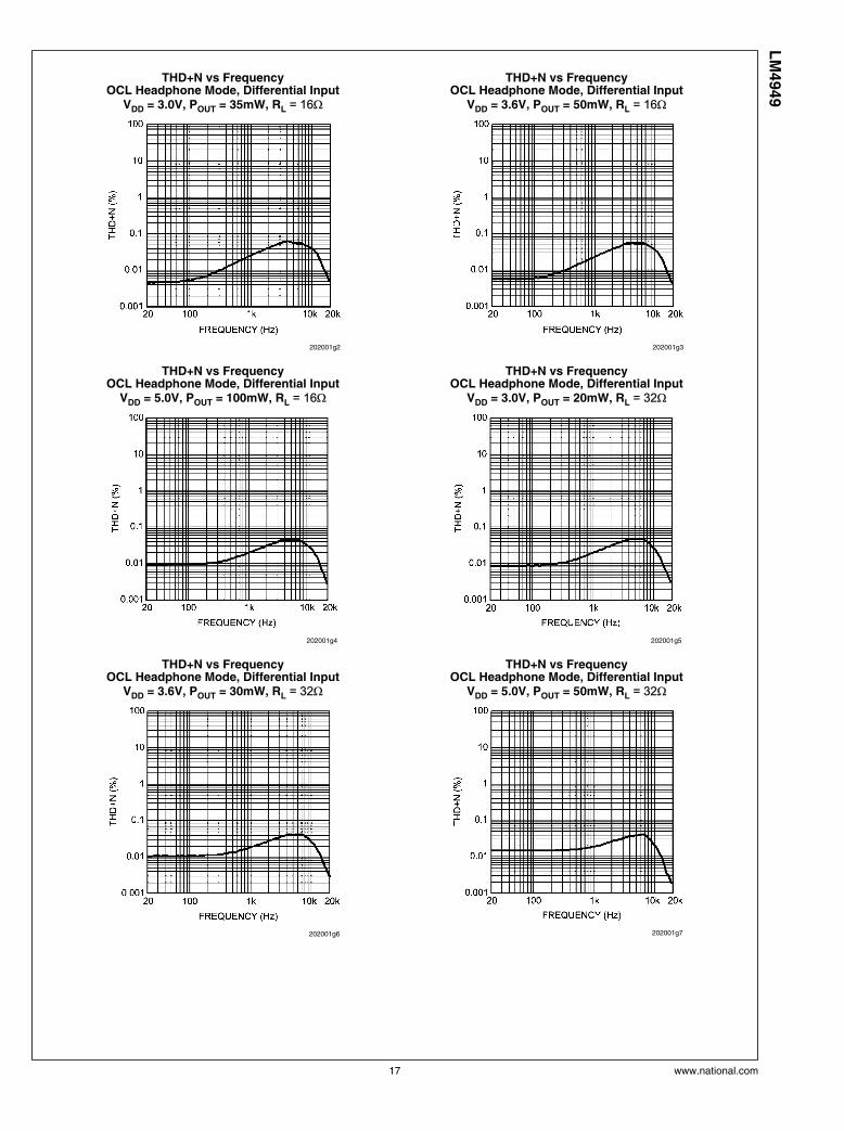
THD+N vs FrequencyOCL Headphone Mode, Differential Input
VDD = 3.0V, POUT = 35mW, RL = 16Ω
202001g2
THD+N vs FrequencyOCL Headphone Mode, Differential Input
VDD = 3.6V, POUT = 50mW, RL = 16Ω
202001g3
THD+N vs FrequencyOCL Headphone Mode, Differential Input
VDD = 5.0V, POUT = 100mW, RL = 16Ω
202001g4
THD+N vs FrequencyOCL Headphone Mode, Differential Input
VDD = 3.0V, POUT = 20mW, RL = 32Ω
202001g5
THD+N vs FrequencyOCL Headphone Mode, Differential Input
VDD = 3.6V, POUT = 30mW, RL = 32Ω
202001g6
THD+N vs FrequencyOCL Headphone Mode, Differential Input
VDD = 5.0V, POUT = 50mW, RL = 32Ω
202001g7
17 www.national.com
LM
4949
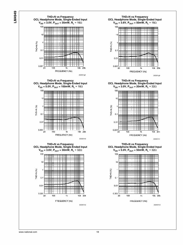
THD+N vs FrequencyOCL Headphone Mode, Single-Ended Input
VDD = 3.0V, POUT = 35mW, RL = 16Ω
202001g8
THD+N vs FrequencyOCL Headphone Mode, Single-Ended Input
VDD = 3.6V, POUT = 50mW, RL = 16Ω
202001g9
THD+N vs FrequencyOCL Headphone Mode, Single-Ended Input
VDD = 5.0V, POUT = 100mW, RL = 16Ω
202001h0
THD+N vs FrequencyOCL Headphone Mode, Single-Ended Input
VDD = 3.0V, POUT = 20mW, RL = 32Ω
202001h1
THD+N vs FrequencyOCL Headphone Mode, Single-Ended Input
VDD = 3.6V, POUT = 30mW, RL = 32Ω
202001h2
THD+N vs FrequencyOCL Headphone Mode, Single-Ended Input
VDD = 5.0V, POUT = 50mW, RL = 32Ω
202001h3
www.national.com 18
LM
4949

THD+N vs FrequencyCC Headphone Mode, Differential Input
VDD = 3.0V, POUT = 35mW, RL = 16Ω
202001h4
THD+N vs FrequencyCC Headphone Mode, Differential Input
VDD = 3.6V, POUT = 50mW, RL = 16Ω
202001h5
THD+N vs FrequencyCC Headphone Mode, Differential Input
VDD = 5.0V, POUT = 100mW, RL = 16Ω
202001h6
THD+N vs FrequencyCC Headphone Mode, Differential Input
VDD = 3.0V, POUT = 20mW, RL = 32Ω
202001h7
THD+N vs FrequencyCC Headphone Mode, Differential Input
VDD = 3.6V, POUT = 30mW, RL = 32Ω
202001h8
THD+N vs FrequencyCC Headphone Mode, Differential Input
VDD = 5.0V, POUT = 50mW, RL = 32Ω
202001h9
19 www.national.com
LM
4949

THD+N vs FrequencyCC Headphone Mode, Single-Ended Input
VDD = 3.0V, POUT = 35mW, RL = 16Ω
202001i3
THD+N vs FrequencyCC Headphone Mode, Single-Ended Input
VDD = 3.6V, POUT = 50mW, RL = 16Ω
202001i4
THD+N vs FrequencyCC Headphone Mode, Single-Ended Input
VDD = 5.0V, POUT = 100mW, RL = 16Ω
202001i5
THD+N vs FrequencyCC Headphone Mode, Single-Ended Input
VDD = 3.0V, POUT = 20mW, RL = 32Ω
202001i6
THD+N vs FrequencyCC Headphone Mode, Single-Ended Input
VDD = 3.6V, POUT = 30mW, RL = 32Ω
202001i7
THD+N vs FrequencyCC Headphone Mode, Single-Ended Input
VDD = 5.0V, POUT = 50mW, RL = 32Ω
202001i8
www.national.com 20
LM
4949
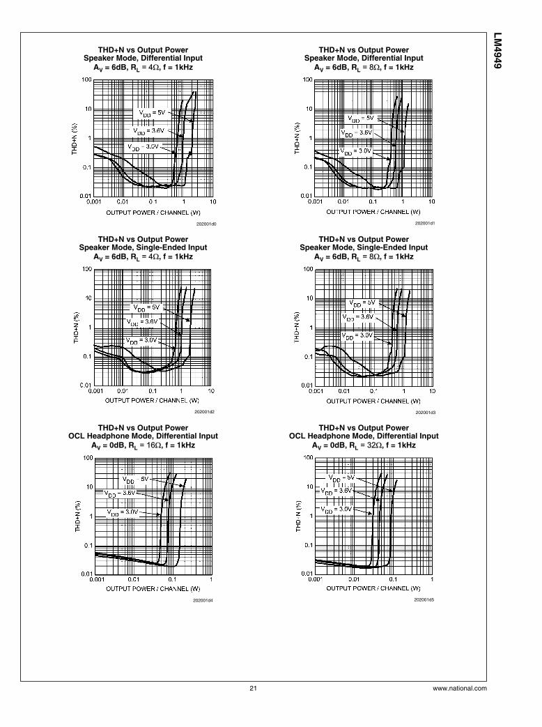
THD+N vs Output PowerSpeaker Mode, Differential Input
AV = 6dB, RL = 4Ω, f = 1kHz
202001d0
THD+N vs Output PowerSpeaker Mode, Differential Input
AV = 6dB, RL = 8Ω, f = 1kHz
202001d1
THD+N vs Output PowerSpeaker Mode, Single-Ended Input
AV = 6dB, RL = 4Ω, f = 1kHz
202001d2
THD+N vs Output PowerSpeaker Mode, Single-Ended Input
AV = 6dB, RL = 8Ω, f = 1kHz
202001d3
THD+N vs Output PowerOCL Headphone Mode, Differential Input
AV = 0dB, RL = 16Ω, f = 1kHz
202001d4
THD+N vs Output PowerOCL Headphone Mode, Differential Input
AV = 0dB, RL = 32Ω, f = 1kHz
202001d5
21 www.national.com
LM
4949
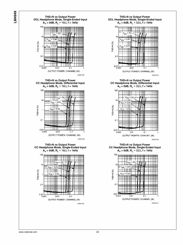
THD+N vs Output PowerOCL Headphone Mode, Single-Ended Input
AV = 0dB, RL = 16Ω, f = 1kHz
202001d6
THD+N vs Output PowerOCL Headphone Mode, Single-Ended Input
AV = 0dB, RL = 32Ω, f = 1kHz
202001d7
THD+N vs Output PowerCC Headphone Mode, Differential Input
AV = 0dB, RL = 16Ω, f = 1kHz
202001d8
THD+N vs Output PowerCC Headphone Mode, Differential Input
AV = 0dB, RL = 32Ω, f = 1kHz
202001d9
THD+N vs Output PowerCC Headphone Mode, Single-Ended Input
AV = 0dB, RL = 16Ω, f = 1kHz
202001e0
THD+N vs Output PowerCC Headphone Mode, Single-Ended Input
AV = 0dB, RL = 32Ω, f = 1kHz
202001e1
www.national.com 22
LM
4949
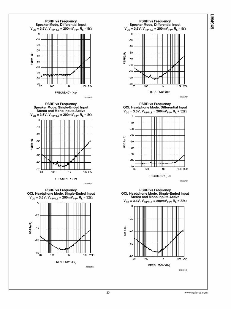
PSRR vs FrequencySpeaker Mode, Differential Input
VDD = 3.6V, VRIPPLE = 200mVP-P, RL = 8Ω
202001i9
PSRR vs FrequencySpeaker Mode, Differential Input
VDD = 3.6V, VRIPPLE = 200mVP-P, RL = 8Ω
202001j0
PSRR vs FrequencySpeaker Mode, Single-Ended Input
Stereo and Mono Inputs ActiveVDD = 3.6V, VRIPPLE = 200mVP-P, RL = 8Ω
202001j1
PSRR vs FrequencyOCL Headphone Mode, Differential InputVDD = 3.6V, VRIPPLE = 200mVP-P, RL = 32Ω
202001j2
PSRR vs FrequencyOCL Headphone Mode, Single-Ended Input
VDD = 3.6V, VRIPPLE = 200mVP-P, RL = 32Ω
202001j3
PSRR vs FrequencyOCL Headphone Mode, Single-Ended Input
Stereo and Mono Inputs ActiveVDD = 3.6V, VRIPPLE = 200mVP-P, RL = 32Ω
202001j4
23 www.national.com
LM
4949
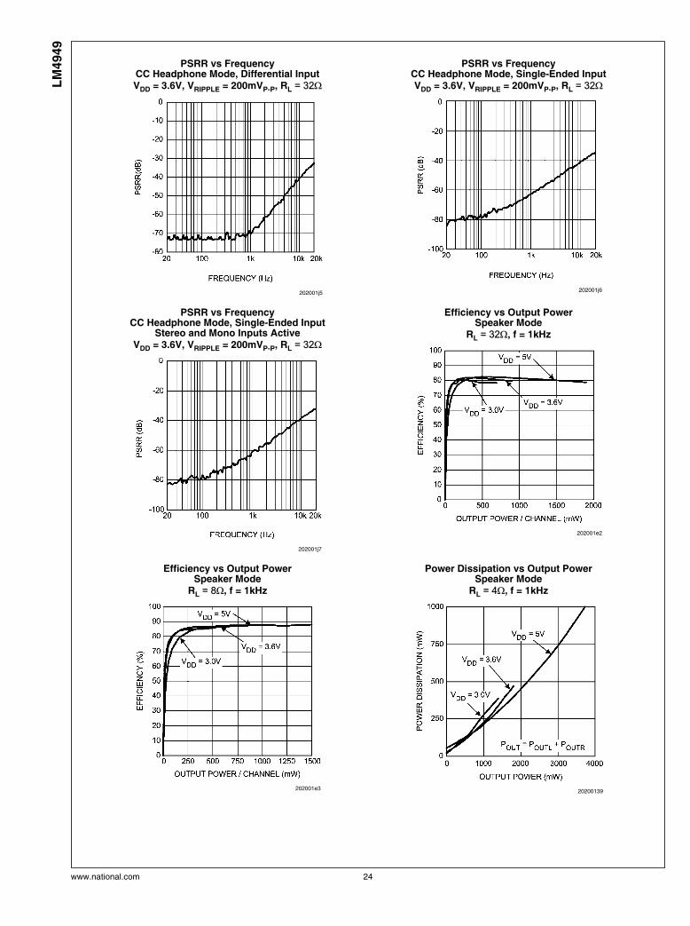
PSRR vs FrequencyCC Headphone Mode, Differential InputVDD = 3.6V, VRIPPLE = 200mVP-P, RL = 32Ω
202001j5
PSRR vs FrequencyCC Headphone Mode, Single-Ended InputVDD = 3.6V, VRIPPLE = 200mVP-P, RL = 32Ω
202001j6
PSRR vs FrequencyCC Headphone Mode, Single-Ended Input
Stereo and Mono Inputs ActiveVDD = 3.6V, VRIPPLE = 200mVP-P, RL = 32Ω
202001j7
Efficiency vs Output PowerSpeaker Mode
RL = 32Ω, f = 1kHz
202001e2
Efficiency vs Output PowerSpeaker Mode
RL = 8Ω, f = 1kHz
202001e3
Power Dissipation vs Output PowerSpeaker Mode
RL = 4Ω, f = 1kHz
20200139
www.national.com 24
LM
4949

Power Dissipation vs Output PowerSpeaker Mode
RL = 8Ω, f = 1kHz
20200140
Power Dissipation vs Output PowerOCL Headphone Mode
RL = 16Ω, f = 1kHz
20200168
Power Dissipation vs Output PowerOCL Headphone Mode
RL = 32Ω, f = 1kHz
20200169
Power Dissipation vs Output PowerCC Headphone Mode
RL = 16Ω, f = 1kHz
20200195
Power Dissipation vs Output PowerCC Headphone Mode
RL = 32Ω, f = 1kHz
20200196
Output Power vs Supply VoltageSpeaker Mode
RL = 4Ω, f = 1kHz
202001e4
25 www.national.com
LM
4949
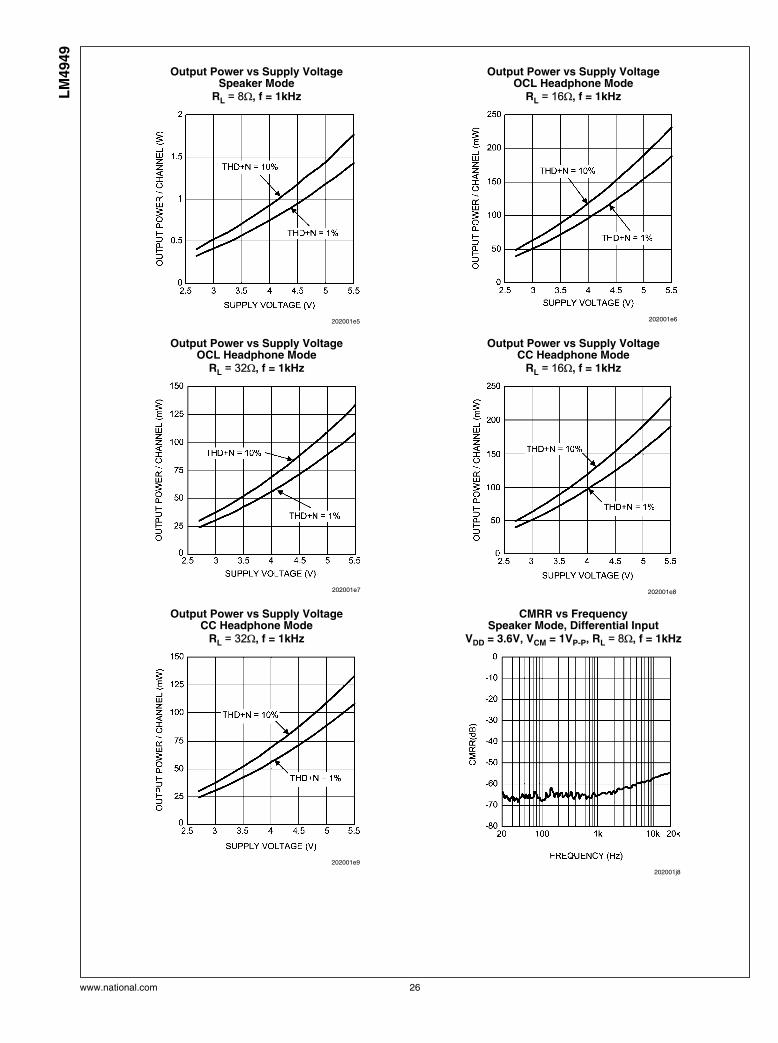
Output Power vs Supply VoltageSpeaker Mode
RL = 8Ω, f = 1kHz
202001e5
Output Power vs Supply VoltageOCL Headphone Mode
RL = 16Ω, f = 1kHz
202001e6
Output Power vs Supply VoltageOCL Headphone Mode
RL = 32Ω, f = 1kHz
202001e7
Output Power vs Supply VoltageCC Headphone Mode
RL = 16Ω, f = 1kHz
202001e8
Output Power vs Supply VoltageCC Headphone Mode
RL = 32Ω, f = 1kHz
202001e9
CMRR vs FrequencySpeaker Mode, Differential Input
VDD = 3.6V, VCM = 1VP-P, RL = 8Ω, f = 1kHz
202001j8
www.national.com 26
LM
4949

CMRR vs FrequencyOCL Headphone Mode
VDD = 3.6V, VCM = 1VP-P, RL = 32Ω
202001j9
CMRR vs FrequencyCC Headphone Mode
VDD = 3.6V, VCM = 1VP-P, RL = 32Ω
202001k3
Output Noise vs FrequencySpeaker Mode, Single-Ended Input
Stereo and Mono Inputs ActiveVDD = 3.6V, RL = 8Ω
202001k0
Output Noise vs FrequencyOCL Headphone Mode, Single-Ended Input
Stereo and Mono Inputs ActiveVDD = 3.6V, RL = 32Ω
202001k1
Output Noise vs FrequencyCC Headphone Mode, Single-Ended Input
Stereo and Mono Inputs ActiveVDD = 3.6V, RL = 32Ω
202001k2
Crosstalk vs FrequencySpeaker Mode
VDD = 3.6V, VRIPPLE = 1VP-P, RL = 8Ω
202001i0
27 www.national.com
LM
4949
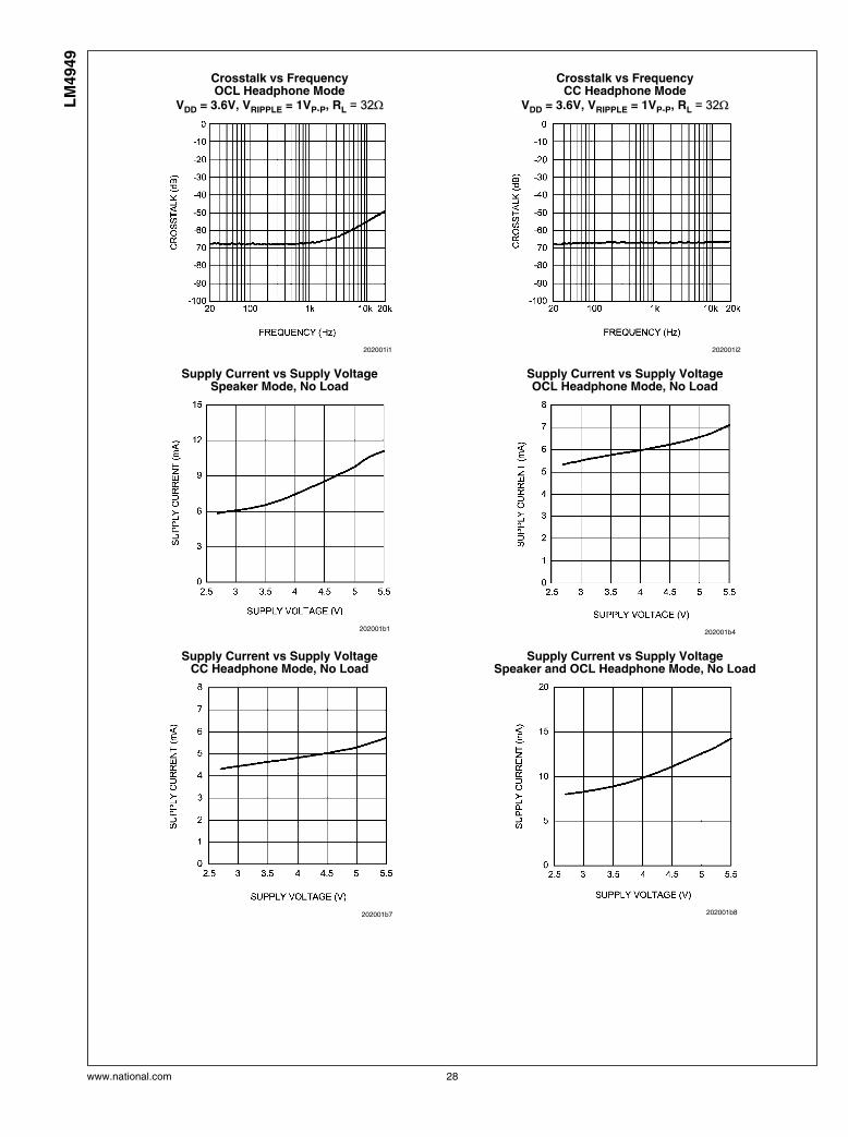
Crosstalk vs FrequencyOCL Headphone Mode
VDD = 3.6V, VRIPPLE = 1VP-P, RL = 32Ω
202001i1
Crosstalk vs FrequencyCC Headphone Mode
VDD = 3.6V, VRIPPLE = 1VP-P, RL = 32Ω
202001i2
Supply Current vs Supply VoltageSpeaker Mode, No Load
202001b1
Supply Current vs Supply VoltageOCL Headphone Mode, No Load
202001b4
Supply Current vs Supply VoltageCC Headphone Mode, No Load
202001b7
Supply Current vs Supply VoltageSpeaker and OCL Headphone Mode, No Load
202001b8
www.national.com 28
LM
4949
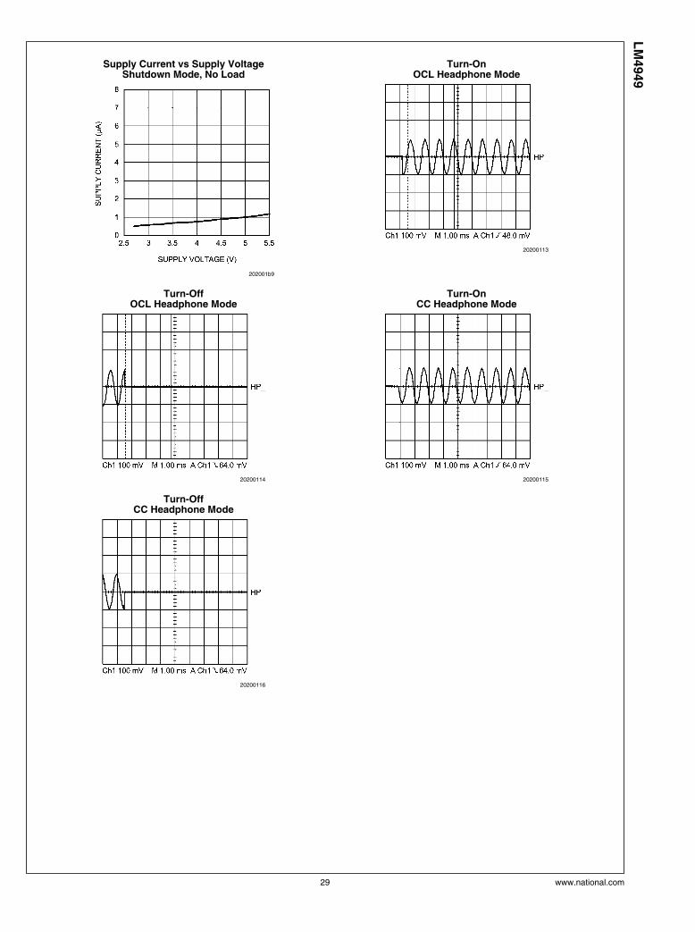
Supply Current vs Supply VoltageShutdown Mode, No Load
202001b9
Turn-OnOCL Headphone Mode
20200113
Turn-OffOCL Headphone Mode
20200114
Turn-OnCC Headphone Mode
20200115
Turn-OffCC Headphone Mode
20200116
29 www.national.com
LM
4949

Application Information
I2C COMPATIBLE INTERFACE
The LM4949 is controlled through an I2C compatible serialinterface that consists of two wires; clock (SCL) and data(SDA). The clock line is uni-directional. The data line is bi-directional (open-collector) although the LM4949 does not
write to the I2C bus. The maximum clock frequency specifiedby the I2C standard is 400kHz.
To avoid an address conflict with another device on the I2Cbus, the LM4949 address is determined by the ADR pin, thestate of ADR determines address bit A1 (Table 2). When ADR= 0, the address is 1111 1000. When ADR = 1 the deviceaddress is 1111 1010.
TABLE 2. Device Address
ADR A7 A6 A5 A4 A3 A2 A1 A0
X 1 1 1 1 1 0 X 0
0 1 1 1 1 1 0 0 0
1 1 1 1 1 1 0 1 0
BUS FORMAT
The I2C bus format is shown in Figure 2. The “start” signal isgenerated by lowering the data signal while the clock is high.The start signal alerts all devices on the bus that a deviceaddress is being written to the bus.
The 8-bit device address is written to the bus next, most sig-nificant bit first. The data is latched in on the rising edge of theclock. Each address bit must be stable while the clock is high.
After the last address bit is sent, the master device releasesthe data line, during which time, an acknowledge clock pulse
is generated. If the LM4949 receives the address correctly,then the LM4949 pulls the data line low, generating an ac-knowledge bit (ACK).
Once the master device has registered the ACK bit, the 8-bitregister address/data word is sent. Each data bit should bestable while the clock level is high. After the 8–bit word is sent,the LM4949 sends another ACK bit. Following the acknowl-edgement of the data word, the master device issues a “stop”bit, allowing SDA to go high while the clock signal is high.
20200109
FIGURE 2. I2C Bus Format
20200110
FIGURE 3. I2C Timing Diagram
www.national.com 30
LM
4949
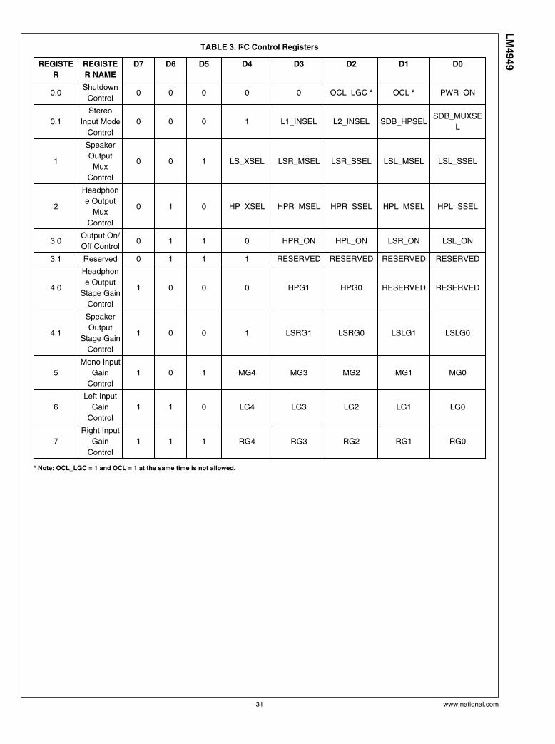
TABLE 3. I2C Control Registers
REGISTE
R
REGISTE
R NAME
D7 D6 D5 D4 D3 D2 D1 D0
0.0Shutdown
Control0 0 0 0 0 OCL_LGC * OCL * PWR_ON
0.1
Stereo
Input Mode
Control
0 0 0 1 L1_INSEL L2_INSEL SDB_HPSELSDB_MUXSE
L
1
Speaker
Output
Mux
Control
0 0 1 LS_XSEL LSR_MSEL LSR_SSEL LSL_MSEL LSL_SSEL
2
Headphon
e Output
Mux
Control
0 1 0 HP_XSEL HPR_MSEL HPR_SSEL HPL_MSEL HPL_SSEL
3.0Output On/
Off Control0 1 1 0 HPR_ON HPL_ON LSR_ON LSL_ON
3.1 Reserved 0 1 1 1 RESERVED RESERVED RESERVED RESERVED
4.0
Headphon
e Output
Stage Gain
Control
1 0 0 0 HPG1 HPG0 RESERVED RESERVED
4.1
Speaker
Output
Stage Gain
Control
1 0 0 1 LSRG1 LSRG0 LSLG1 LSLG0
5
Mono Input
Gain
Control
1 0 1 MG4 MG3 MG2 MG1 MG0
6
Left Input
Gain
Control
1 1 0 LG4 LG3 LG2 LG1 LG0
7
Right Input
Gain
Control
1 1 1 RG4 RG3 RG2 RG1 RG0
* Note: OCL_LGC = 1 and OCL = 1 at the same time is not allowed.
31 www.national.com
LM
4949
GENERAL AMPLIFIER FUNCTION
Class D Amplifier
The LM4949 features a high-efficiency, filterless, Class Dstereo amplifier. The LM4949 Class D amplifiers feature a fil-terless modulation scheme, the differential outputs of eachchannel switch at 300khz, from VDD to GND. When there isno input signal applied, the two outputs (_LS+ and _LS-)switch with a 50% duty cycle, with both outputs in phase. Be-cause the outputs of the LM4949 are differential, the twosignals cancel each other. This results in no net voltageacross the speaker, thus no load current during the idle state,conserving power.
When an input signal is applied, the duty cycle (pulse width)changes. For increasing output voltages, the duty cycle of_LS+ increases, while the duty cycle of _LS- decreases. Fordecreasing output voltages, the converse occurs, the dutycycle of _LS- increases while the duty cycle of _LS+ decreas-es. The difference between the two pulse widths yields thedifferential output voltage.
Headphone Amplifier
The LM4949 headphone amplifier features three different op-erating modes, output capacitorless (OCL), capacitor-cou-pled (CC), and external amplifier mode.
The OCL architecture eliminates the bulky, expensive outputcoupling capacitors required by traditional headphone ampli-fiers. The LM4949 headphone section uses three amplifiers.Two amplifiers drive the headphones while the third (VOC) isset to the internally generated bias voltage (typically VDD/2).The third amplifier is connected to the return terminal of theheadphone jack. In this configuration, the signal side of theheadphones are biased to VDD/2, the return is biased toVDD/2, thus there is no net DC voltage across the headphone,eliminating the need for an output coupling capacitor. Re-
moving the output coupling capacitors from the headphonesignal path reduces component count, reducing system costand board space consumption, as well as improving low fre-quency performance.
In OCL mode, the headphone return sleeve is biased toVDD/2. When driving headphones, the voltage on the returnsleeve is not an issue. However, if the headphone output isused as a line out, the VDD/2 can conflict with the GND po-tential that a line-in would expect on the return sleeve. Whenthe return of the headphone jack is connected to GND, theVOC amplifier of the LM4949 detects an output short circuitcondition and is disabled, preventing damage to the LM4949,and allowing the headphone return to be biased at GND.
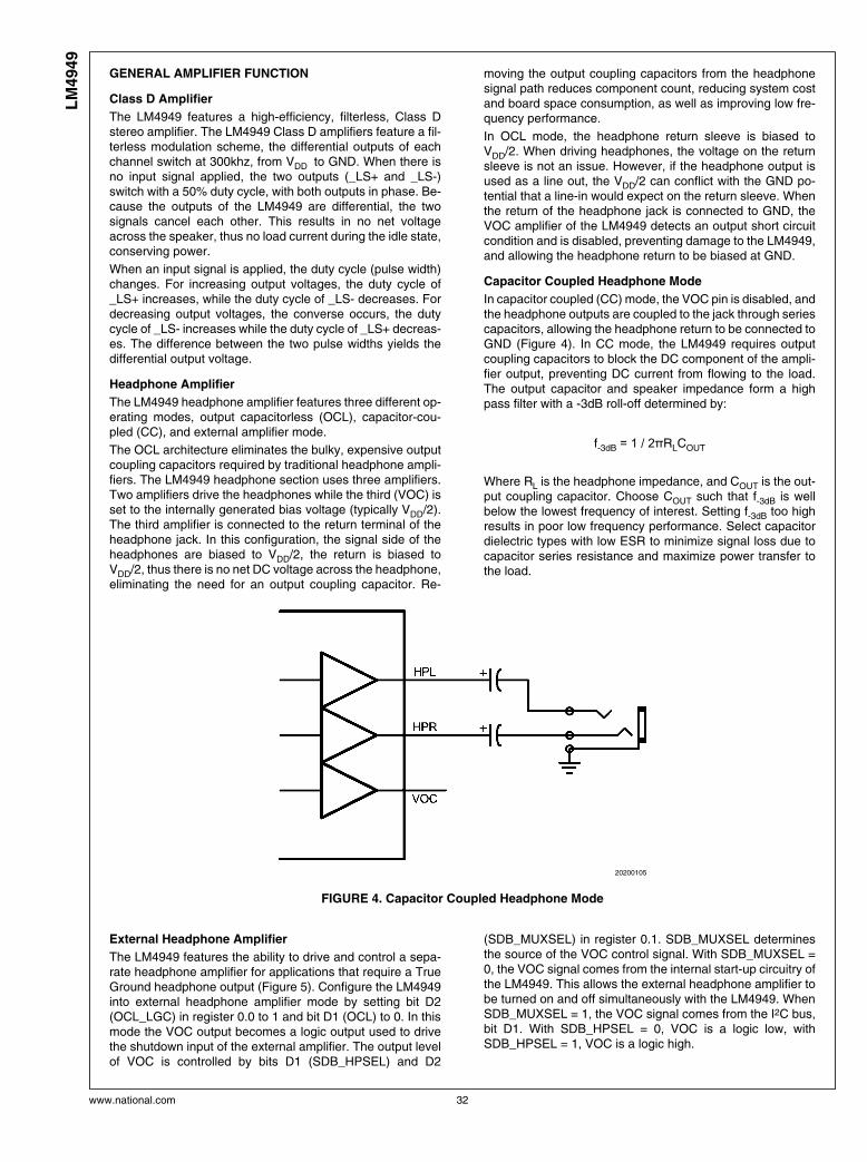
Capacitor Coupled Headphone Mode
In capacitor coupled (CC) mode, the VOC pin is disabled, andthe headphone outputs are coupled to the jack through seriescapacitors, allowing the headphone return to be connected toGND (Figure 4). In CC mode, the LM4949 requires outputcoupling capacitors to block the DC component of the ampli-fier output, preventing DC current from flowing to the load.The output capacitor and speaker impedance form a highpass filter with a -3dB roll-off determined by:
f-3dB = 1 / 2πRLCOUT
Where RL is the headphone impedance, and COUT is the out-put coupling capacitor. Choose COUT such that f-3dB is wellbelow the lowest frequency of interest. Setting f-3dB too highresults in poor low frequency performance. Select capacitordielectric types with low ESR to minimize signal loss due tocapacitor series resistance and maximize power transfer tothe load.
20200105
FIGURE 4. Capacitor Coupled Headphone Mode
External Headphone Amplifier
The LM4949 features the ability to drive and control a sepa-rate headphone amplifier for applications that require a TrueGround headphone output (Figure 5). Configure the LM4949into external headphone amplifier mode by setting bit D2(OCL_LGC) in register 0.0 to 1 and bit D1 (OCL) to 0. In thismode the VOC output becomes a logic output used to drivethe shutdown input of the external amplifier. The output levelof VOC is controlled by bits D1 (SDB_HPSEL) and D2
(SDB_MUXSEL) in register 0.1. SDB_MUXSEL determinesthe source of the VOC control signal. With SDB_MUXSEL =0, the VOC signal comes from the internal start-up circuitry ofthe LM4949. This allows the external headphone amplifier tobe turned on and off simultaneously with the LM4949. WhenSDB_MUXSEL = 1, the VOC signal comes from the I2C bus,bit D1. With SDB_HPSEL = 0, VOC is a logic low, withSDB_HPSEL = 1, VOC is a logic high.
www.national.com 32
LM
4949

202001c8
FIGURE 5. Driving an External Headphone Amplifier
33 www.national.com
LM
4949
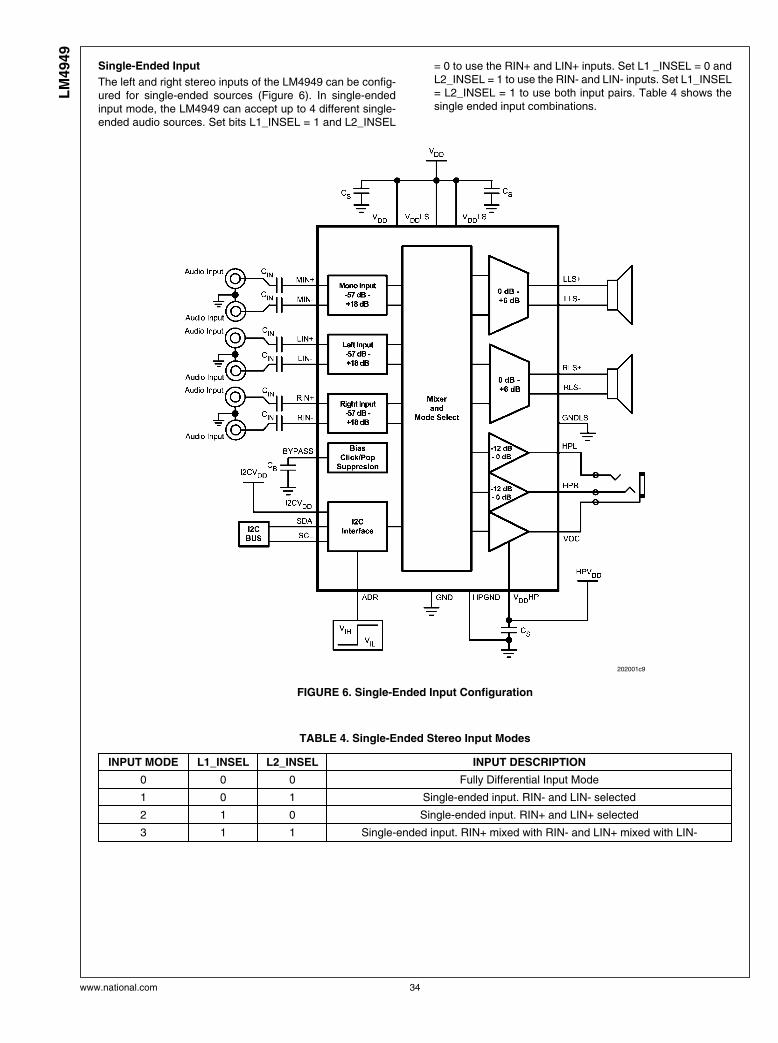
Single-Ended Input
The left and right stereo inputs of the LM4949 can be config-ured for single-ended sources (Figure 6). In single-endedinput mode, the LM4949 can accept up to 4 different single-ended audio sources. Set bits L1_INSEL = 1 and L2_INSEL
= 0 to use the RIN+ and LIN+ inputs. Set L1 _INSEL = 0 andL2_INSEL = 1 to use the RIN- and LIN- inputs. Set L1_INSEL= L2_INSEL = 1 to use both input pairs. Table 4 shows thesingle ended input combinations.
202001c9
FIGURE 6. Single-Ended Input Configuration
TABLE 4. Single-Ended Stereo Input Modes
INPUT MODE L1_INSEL L2_INSEL INPUT DESCRIPTION
0 0 0 Fully Differential Input Mode
1 0 1 Single-ended input. RIN- and LIN- selected
2 1 0 Single-ended input. RIN+ and LIN+ selected
3 1 1 Single-ended input. RIN+ mixed with RIN- and LIN+ mixed with LIN-
www.national.com 34
LM
4949
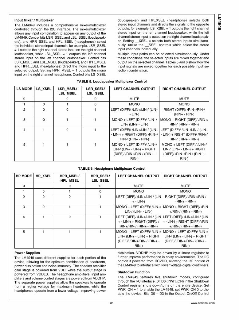
Input Mixer / Multiplexer
The LM4949 includes a comprehensive mixer/multiplexercontrolled through the I2C interface. The mixer/multiplexerallows any input combination to appear on any output of theLM4949. Control bits LSR_SSEL and LSL_SSEL (loudspeak-ers), and HPR_SSEL and HPL_SSEL (headphones) selectthe individual stereo input channels; for example, LSR_SSEL= 1 outputs the right channel stereo input on the right channelloudspeaker, while LSL_SSEL = 1 outputs the left channelstereo input on the left channel loudspeaker. Control bitsLSR_MSEL and LSL_MSEL (loudspeaker), and HPR_MSELand HPR_LSEL (headphones) direct the mono input to theselected output. Setting HPR_MSEL = 1 outputs the monoinput on the right channel headphone. Control bits LS_XSEL
(loudspeaker) and HP_XSEL (headphone) selects bothstereo input channels and directs the signals to the oppositeoutputs, for example, LS_XSEL = 1 outputs the right channelstereo input on the left channel loudspeaker, while the leftchannel stereo input is output on the right channel loudspeak-er. Setting __XSEL = selects both stereo inputs simultane-ously, unlike the __SSEL controls which select the stereoinput channels individually.
Multiple input paths can be selected simultaneously. Underthese conditions, the selected inputs are mixed together andoutput on the selected channel. Tables 5 and 6 show how theinput signals are mixed together for each possible input se-lection combination.
TABLE 5. Loudspeaker Multiplexer Control
LS MODE LS_XSEL LSR_MSEL/
LSL_MSEL
LSR_SSEL/
LSL_SSEL
LEFT CHANNEL OUTPUT RIGHT CHANNEL OUTPUT
0 0 0 MUTE MUTE
1 0 1 0 MONO MONO
2 0 0 1 LEFT (DIFF)/ /LIN+/LIN-/ (LIN+
- LIN-)
RIGHT (DIFF)/ /RIN+/RIN-/
(RIN+ - RIN-)
3 0 1 1 MONO + LEFT (DIFF)/ /LIN+/
LIN-/ (LIN+ - LIN-)
MONO + RIGHT (DIFF)/ /RIN+/
RIN-/ (RIN+ - RIN-)
4 1 0 1 LEFT (DIFF)/ /LIN+/LIN-/ (LIN+
- LIN-) + RIGHT (DIFF)/ /RIN+/
RIN-/ (RIN+ - RIN-)
LEFT (DIFF)/ /LIN+/LIN-/ (LIN+
- LIN-) + RIGHT (DIFF)/ /RIN+/
RIN-/ (RIN+ - RIN-)
5 1 1 1 MONO + LEFT (DIFF)/ /LIN+/
LIN-/ (LIN+ - LIN-) + RIGHT
(DIFF)/ /RIN+/RIN-/ (RIN+ -
RIN-)
MONO + LEFT (DIFF)/ /LIN+/
LIN-/ (LIN+ - LIN-) + RIGHT
(DIFF)/ /RIN+/RIN-/ (RIN+ -
RIN-)
TABLE 6. Headphone Multiplexer Control
HP MODE HP_XSEL HPR_MSEL/
HPL_MSEL
HPR_SSEL/
LSL_SSEL
LEFT CHANNEL OUTPUT RIGHT CHANNEL OUTPUT
0 0 0 MUTE MUTE
1 0 1 0 MONO MONO
2 0 0 1 LEFT (DIFF)/ /LIN+/LIN-/ (LIN
+ - LIN-)
RIGHT (DIFF)/ /RIN+/RIN-/
(RIN+ - RIN-)
3 0 1 1 MONO + LEFT (DIFF)/ /LIN+/
LIN-/ (LIN+ - LIN-)
MONO + RIGHT (DIFF)/ /RIN
+/RIN-/ (RIN+ - RIN-)
4 1 0 1 LEFT (DIFF)/ /LIN+/LIN-/ (LIN
+ - LIN-) + RIGHT (DIFF)/ /
RIN+/RIN-/ (RIN+ - RIN-)
LEFT (DIFF)/ /LIN+/LIN-/ (LIN
+ - LIN-) + RIGHT (DIFF)/ /RIN
+/RIN-/ (RIN+ - RIN-)
5 1 1 1 MONO + LEFT (DIFF)/ /LIN+/
LIN-/ (LIN+ - LIN-) + RIGHT
(DIFF)/ /RIN+/RIN-/ (RIN+ -
RIN-)
MONO + LEFT (DIFF)/ /LIN+/
LIN-/ (LIN+ - LIN-) + RIGHT
(DIFF)/ /RIN+/RIN-/ (RIN+ -
RIN-)
Power Supplies
The LM4949 uses different supplies for each portion of thedevice, allowing for the optimum combination of headroom,power dissipation and noise immunity. The speaker amplifiergain stage is powered from VDD, while the output stage ispowered from VDDLS. The headphone amplifiers, input am-plifiers and volume control stages are powered from VDDHP.The separate power supplies allow the speakers to operatefrom a higher voltage for maximum headroom, while theheadphones operate from a lower voltage, improving power
dissipation. VDDHP may be driven by a linear regulator tofurther improve performance in noisy environments. The I2Cportion if powered from I2CVDD, allowing the I2C portion ofthe LM4949 to interface with lower voltage digital controllers.
Shutdown Function
The LM4949 features five shutdown modes, configuredthrough the I2C interface. Bit D0 (PWR_ON) in the ShutdownControl register shuts down/turns on the entire device. SetPWR_ON = 1 to enable the LM4949, set PWR_ON 0 to dis-able the device. Bits D0 – D3 in the Output On/Off Control
35 www.national.com
LM
4949

shutdown/turn on the individual channels. HPR_ON (D3) con-trols the right channel headphone output, HPL_ON (D2) con-trols the left channel headphone output, LSR_ON (D1)controls the right channel loudspeaker output, and LRL_ON(D0) controls the left channel loudspeaker output. ThePWR_ON bit takes precedence over the individual channelcontrols.
Audio Amplifier Gain Setting
The each channel of the LM4949 has two separate gainstages. Each input stage features a 32 step volume controlwith a range of -57dB to +18dB (Table 7). Each speaker out-put stage has 4 gain settings (Table 8); 0dB, 2dB, 4dB, and6dB when either a fully differential signal or two single endedsignals are applied on the _IN+ and _IN- pins; and 6dB, 8dB,
10dB and 12dB in single-ended input mode with only one sig-nal applied. The headphone gain is not affected by the inputmode. Each headphone output stage has 3 gain settings (Ta-ble 9), 0dB, -6dB, and -12dB. This allows for a maximumseparation of 24dB between the speaker and headphone out-puts when both are active.
Calculate the total gain of a given signal path as follows:
AVOL + AOS = ATOTAL
Where AVOL is the volume control level, AOS is the gain settingof the output stage, and ATOTAL is the total gain for the signalpath.
www.national.com 36
LM
4949
TABLE 7. 32 Step Volume Control
Volume Step MG4/LG4/RG4 MG3/LG3/RG3 MG2/LG2/RG2 MG1/LG1/RG1 MG0/LG0/RG0 Gain (dB)
1 0 0 0 0 0 –57
2 0 0 0 0 1 –49
3 0 0 0 1 0 –42
4 0 0 0 1 1 –34.5
5 0 0 1 0 0 –30.5
6 0 0 1 0 1 –27
7 0 0 1 1 0 –24
8 0 0 1 1 1 –21
9 0 1 0 0 0 –18
10 0 1 0 0 1 –15
11 0 1 0 1 0 –13.5
12 0 1 0 1 1 –12
13 0 1 1 0 0 –10.5
14 0 1 1 0 1 –9
15 0 1 1 1 0 –7.5
16 0 1 1 1 1 –6
17 1 0 0 0 0 –4.5
18 1 0 0 0 1 –3
19 1 0 0 1 0 –1.5
20 1 0 0 1 1 0
21 1 0 1 0 0 1.5
22 1 0 1 0 1 3
23 1 0 1 1 0 4.5
24 1 0 1 1 1 6
25 1 1 0 0 0 7.5
26 1 1 0 0 1 9
27 1 1 0 1 0 10.5
28 1 1 0 1 1 12
29 1 1 1 0 0 13.5
30 1 1 1 0 1 15
31 1 1 1 1 0 16.5
32 1 1 1 1 1 18
TABLE 8. Loudspeaker Gain Setting
LSRG1/LSLG1 LSRG0/LSLG0Gain (dB)
_IN+ ≠ _IN- _IN+ =_IN-
0 0 12 6
0 1 10 4
1 0 8 2
1 1 6 0
TABLE 9. Headphone Gain Setting
HPG1 HPG0 Gain (dB)
0 0 0
0 1 –6
1 0 –12
37 www.national.com
LM
4949
Differential Audio Amplifier Configuration
As logic supply voltages continue to shrink, system designersincreasingly turn to differential signal handling to preservesignal to noise ratio with decreasing voltage swing. TheLM4949 can be configured as a fully differential amplifier,amplifying the difference between the two inputs. The advan-tage of the differential architecture is any signal componentthat is common to both inputs is rejected, improving common-mode rejection (CMRR) and increasing the SNR of the am-plifier by 6dB over a single-ended architecture. The improvedCMRR and SNR of a differential amplifier reduce sensitivityto ground offset related noise injection, especially importantin noisy applications such as cellular phones. Driving theLM4949 differentially also allows the inputs to be DC coupled,eliminating two external capacitors per channel. Set bitsL1_INSEL and L2_INSEL = 0 for differential input mode. Theleft and right stereo inputs have selectable differential or sin-gle-ended input modes, while the mono input is always dif-ferential.
Single-Ended Audio Amplifier Configuration
In single-ended input mode, the audio sources must be ca-pacitively coupled to the LM4949. With LIN+ ≠ LIN- and RIN+ ≠ RIN-, the loud speaker gain is 6dB more than in differentialinput mode, or when LIN+ = LIN- and RIN+ = RIN-. The head-phone gain does not change. The mono input channel is notaffected by L1_INSEL and L2_INSEL, and is always config-ured as a differential input.
Power Dissipation and Efficiency
The major benefit of Class D amplifiers is increased efficiencyversus Class AB. The efficiency of the LM4949 speaker am-plifiers is attributed to the output transistors’ region of opera-tion. The Class D output stage acts as current steeringswitches, consuming negligible amounts of power comparedto their Class AB counterparts. Most of the power loss asso-ciated with the output stage is due to the IR loss of theMOSFET on-resistance, along with the switching losses dueto gate charge.
The maximum power dissipation per headphone channel inCapacitor-Coupled mode is given by:
PDMAX = VDD2 / 2π2RL
In OCL mode, the maximum power dissipation per head-phone channel increases due to the use of a third amplifier asa buffer. The power dissipation is given by:
PDMAX = VDD2 / π2RL
PROPER SELECTION OF EXTERNAL COMPONENTS
Audio Amplifier Power Supply Bypassing / Filtering
Proper power supply bypassing is critical for low noise per-formance and high PSRR. Place the supply bypass capaci-
tors as close to the device as possible. Typical applicationsemploy a voltage regulator with 10µF and 0.1µF bypass ca-pacitors that increase supply stability. These capacitors donot eliminate the need for bypassing of the LM4949 supplypins. A 1µF ceramic capacitor placed close to each supply pinis recommended.
Bypass Capacitor Selection
The LM4949 generates a VDD/2 common-mode bias voltageinternally. The BYPASS capacitor, CB, improves PSRR andTHD+N by reducing noise at the BYPASS node. Use a 1µFcapacitor, placed as close to the device as possible for CB.
Audio Amplifier Input Capacitor Selection
Input capacitors, CIN, in conjunction with the input impedanceof the LM4949 forms a high pass filter that removes the DCbias from an incoming signal. The AC-coupling capacitor al-lows the amplifier to bias the signal to an optimal DC level.Assuming zero source impedance, the -3dB point of the highpass filter is given by:
f-3dB = 1 / 2πRINCIN
Choose CIN such that f-3dB is well below the lowest frequencyof interest. Setting f-3dB too high affects the low-frequency re-sponse of the amplifier. Use capacitors with low voltage co-efficient dielectrics, such as tantalum or aluminum electrolyt-ic. Capacitors with high-voltage coefficients, such asceramics, may result in increased distortion at low frequen-cies. Other factors to consider when designing the input filterinclude the constraints of the overall system. Although highfidelity audio requires a flat frequency response between20Hz and 20kHz, portable devices such as cell phones mayonly concentrate on the frequency range of the spoken humanvoice (typically 300Hz to 4kHz). In addition, the physical sizeof the speakers used in such portable devices limits the lowfrequency response; in this case, frequencies below 150Hzmay be filtered out.
PCB LAYOUT GUIDELINES
Minimize trace impedance of the power, ground and all outputtraces for optimum performance. Voltage loss due to traceresistance between the LM4949 and the load results in de-creased output power and efficiency. Trace resistance be-tween the power supply and GND of the LM4949 has thesame effect as a poorly regulated supply, increased ripple andreduced peak output power. Use wide traces for power-sup-ply inputs and amplifier outputs to minimize losses due totrace resistance, as well as route heat away from the device.Proper grounding improves audio performance, minimizescrosstalk between channels and prevents switching noisefrom interfering with the audio signal. Use of power andground planes is recommended.
Place all digital components and digital signal traces as far aspossible from analog components and traces. Do not run dig-ital and analog traces in parallel on the same PCB layer.
www.national.com 38
LM
4949

Revision History
Rev Date Description
1.0 09/06/06 Initial release.
1.1 09/27/06 Fixed some of the Typical Performance Curves.
1.2 01/17/07 Added the X1, X2, and X3 numerical values of theTLA25JJA mktg outline (back
page).
39 www.national.com
LM
4949

Physical Dimensions inches (millimeters) unless otherwise noted
micro SMD PackageOrder Number LM4949TL
NS Package Number TLA25JJAX1 = 2.722, X2 = 2.722, X3 = 0.600
www.national.com 40
LM
4949
Notes
41 www.national.com
LM
4949
NotesL
M4949 S
tere
o C
lass D
Au
dio
Su
bsyste
m w
ith
OC
L H
ead
ph
on
e A
mp
lifi
er
THE CONTENTS OF THIS DOCUMENT ARE PROVIDED IN CONNECTION WITH NATIONAL SEMICONDUCTOR CORPORATION(“NATIONAL”) PRODUCTS. NATIONAL MAKES NO REPRESENTATIONS OR WARRANTIES WITH RESPECT TO THE ACCURACYOR COMPLETENESS OF THE CONTENTS OF THIS PUBLICATION AND RESERVES THE RIGHT TO MAKE CHANGES TOSPECIFICATIONS AND PRODUCT DESCRIPTIONS AT ANY TIME WITHOUT NOTICE. NO LICENSE, WHETHER EXPRESS,IMPLIED, ARISING BY ESTOPPEL OR OTHERWISE, TO ANY INTELLECTUAL PROPERTY RIGHTS IS GRANTED BY THISDOCUMENT.
TESTING AND OTHER QUALITY CONTROLS ARE USED TO THE EXTENT NATIONAL DEEMS NECESSARY TO SUPPORTNATIONAL’S PRODUCT WARRANTY. EXCEPT WHERE MANDATED BY GOVERNMENT REQUIREMENTS, TESTING OF ALLPARAMETERS OF EACH PRODUCT IS NOT NECESSARILY PERFORMED. NATIONAL ASSUMES NO LIABILITY FORAPPLICATIONS ASSISTANCE OR BUYER PRODUCT DESIGN. BUYERS ARE RESPONSIBLE FOR THEIR PRODUCTS ANDAPPLICATIONS USING NATIONAL COMPONENTS. PRIOR TO USING OR DISTRIBUTING ANY PRODUCTS THAT INCLUDENATIONAL COMPONENTS, BUYERS SHOULD PROVIDE ADEQUATE DESIGN, TESTING AND OPERATING SAFEGUARDS.
EXCEPT AS PROVIDED IN NATIONAL’S TERMS AND CONDITIONS OF SALE FOR SUCH PRODUCTS, NATIONAL ASSUMES NOLIABILITY WHATSOEVER, AND NATIONAL DISCLAIMS ANY EXPRESS OR IMPLIED WARRANTY RELATING TO THE SALEAND/OR USE OF NATIONAL PRODUCTS INCLUDING LIABILITY OR WARRANTIES RELATING TO FITNESS FOR A PARTICULARPURPOSE, MERCHANTABILITY, OR INFRINGEMENT OF ANY PATENT, COPYRIGHT OR OTHER INTELLECTUAL PROPERTYRIGHT.
LIFE SUPPORT POLICY
NATIONAL’S PRODUCTS ARE NOT AUTHORIZED FOR USE AS CRITICAL COMPONENTS IN LIFE SUPPORT DEVICES ORSYSTEMS WITHOUT THE EXPRESS PRIOR WRITTEN APPROVAL OF THE CHIEF EXECUTIVE OFFICER AND GENERALCOUNSEL OF NATIONAL SEMICONDUCTOR CORPORATION. As used herein:
Life support devices or systems are devices which (a) are intended for surgical implant into the body, or (b) support or sustain life andwhose failure to perform when properly used in accordance with instructions for use provided in the labeling can be reasonably expectedto result in a significant injury to the user. A critical component is any component in a life support device or system whose failure to performcan be reasonably expected to cause the failure of the life support device or system or to affect its safety or effectiveness.
National Semiconductor and the National Semiconductor logo are registered trademarks of National Semiconductor Corporation. All otherbrand or product names may be trademarks or registered trademarks of their respective holders.
Copyright© 2007 National Semiconductor Corporation
For the most current product information visit us at www.national.com
National SemiconductorAmericas CustomerSupport CenterEmail:[email protected]: 1-800-272-9959
National Semiconductor EuropeCustomer Support CenterFax: +49 (0) 180-530-85-86Email: [email protected] Tel: +49 (0) 69 9508 6208English Tel: +49 (0) 870 24 0 2171Français Tel: +33 (0) 1 41 91 8790
National Semiconductor AsiaPacific Customer Support CenterEmail: [email protected]
National Semiconductor JapanCustomer Support CenterFax: 81-3-5639-7507Email: [email protected]: 81-3-5639-7560
www.national.com