Embed Size (px)
Citation preview

Parallel Flash Loader IP Core User Guide2016.06.01
UG-01082 Subscribe Send Feedback
This document describes how to instantiate the Parallel Flash Loader (PFL) IP core in your design,programming flash memory, and configuring your FPGA from the flash memory.
FPGAs’ increasing density requires larger configuration storage. If your system contains a flash memorydevice, you can use your flash memory as the FPGA configuration storage as well. You can use the PFL IPcore in Altera® MAX® Series (MAX II, MAX V and MAX 10 devices) or all other FPGAs to programflash memory devices efficiently through the JTAG interface and to control configuration from the flashmemory device to the Altera FPGA.
Related Information
• Introduction to Altera IP CoresProvides general information about all Altera IP cores, including parameterizing, generating,upgrading, and simulating IP.
• Creating Version-Independent IP and Qsys Simulation ScriptsCreate simulation scripts that do not require manual updates for software or IP version upgrades.
• Project Management Best PracticesGuidelines for efficient management and portability of your project and IP files.
• Parallel Flash Loader IP Core User Guide Archives on page 54Provides a list of user guides for previous versions of the Parallel Flash Loader IP core.
FeaturesUse the PFL IP core to:
• Program Common Flash Interface (CFI) flash, quad Serial Peripheral Interface (SPI) flash, or NANDflash memory devices with the device JTAG interface.
• Control Altera FPGA configuration from a CFI flash, quad SPI flash, or NAND flash memory devicefor Arria series, Cyclone series, and Stratix series FPGA devices.
Device SupportThis user guide focuses on implementing the PFL IP core in an Altera CPLD. The PFL IP core supports allAltera FPGAs. You can implement the PFL IP core in an Arria®, Cyclone®, or Stratix® device familyFPGA to program flash memory or to configure other FPGAs.
© 2016 Altera Corporation. All rights reserved. ALTERA, ARRIA, CYCLONE, ENPIRION, MAX, MEGACORE, NIOS, QUARTUS and STRATIX words and logos aretrademarks of Altera Corporation and registered in the U.S. Patent and Trademark Office and in other countries. All other words and logos identified astrademarks or service marks are the property of their respective holders as described at www.altera.com/common/legal.html. Altera warrants performanceof its semiconductor products to current specifications in accordance with Altera's standard warranty, but reserves the right to make changes to anyproducts and services at any time without notice. Altera assumes no responsibility or liability arising out of the application or use of any information,product, or service described herein except as expressly agreed to in writing by Altera. Altera customers are advised to obtain the latest version of devicespecifications before relying on any published information and before placing orders for products or services.
ISO9001:2008Registered
www.altera.com101 Innovation Drive, San Jose, CA 95134

Related InformationAN478: Using FPGA-Based Parallel Flash Loader with the Quartus II SoftwareProvides more information about using the FPGA-based PFL IP core to program a flash memory device.
Supported Flash Memory DevicesThe software generates the PFL IP core logic for the flash programming bridge and FPGA configuration.
Table 1: CFI Flash Memory Devices Supported by PFL IP Core
If your CFI device is not in the following table, but is compatible with an Intel or Spansion CFI flash device, Alterarecommends selecting Define CFI Flash Device in the software.
Manufacturer Product Family Data Width Density (Megabit) Device Name(1)(2)
Micron
C3 16
8 28F800C316 28F160C332 28F320C364 28F640C3
J38 or 16
32 28F320J364 28F640J3
128 28F128J316 256 JS29F256J3
P30 16
64 28F640P30128 28F128P30256 28F256P30512 28F512P30
1000 28F00AP302000 28F00BP30
P33 16
128 28F128P33256 28F256P33512 28F512P33640 28F640P33
1000 28F00AP332000 28F00BP33
(1) Spansion has discontinued the Spansion S29GL-N flash memory device family. Altera does not recommendusing this flash memory device. For more information about an alternative recommendation, see relatedinformation.
(2) The PFL IP core supports top and bottom boot block of the flash memory devices. For Micron flash memorydevices, the PFL IP core supports top, bottom, and symmetrical blocks of flash memory devices.
2 Supported Flash Memory DevicesUG-01082
2016.06.01
Altera Corporation Parallel Flash Loader IP Core User Guide
Send Feedback

Manufacturer Product Family Data Width Density (Megabit) Device Name(1)(2)
M29EW 8 or 16
256 28F256M29EW
512 28F512M29EW1000 28F00AM29EW
M29W 8 or 16
16
M28W160CTM28W160CBM29W160F7M29W160FB
32M29W320EM29W320FTM29W320FB
64M29W640FM29W640G
128 M29W128G256 M29W256G
M29DW 8 or 16 32M29DW323DTM29DW323DB
G18 16
512 MT28GU512AAA1EGC-0SIT
1024 MT28GU01GAAA1EGC-0SIT
M58BW32
16M58BW16FTM58BW16FB
32 M58BW32FT16 or 32 32 M58BW32FB
(1) Spansion has discontinued the Spansion S29GL-N flash memory device family. Altera does not recommendusing this flash memory device. For more information about an alternative recommendation, see relatedinformation.
(2) The PFL IP core supports top and bottom boot block of the flash memory devices. For Micron flash memorydevices, the PFL IP core supports top, bottom, and symmetrical blocks of flash memory devices.
UG-010822016.06.01 Supported Flash Memory Devices 3
Parallel Flash Loader IP Core User Guide Altera Corporation
Send Feedback

Manufacturer Product Family Data Width Density (Megabit) Device Name(1)(2)
Spansion
GL-P(3) 8 or 16
128 S29GL128P
256 S29GL256P512 S29GL512P
1024 S29GL01GP
AL-D 8 or 1616 S29AL016D32 S29AL032D
AL-J 8 or 16 16 S29AL016JAL-M 8 or 16 16 S29AL016M
JL-H 8 or 1632 S29JL032H64 S29JL064H
WS-N 16 128 S29WS128N
GL-S 16
128 S29GL128S256 S29GL256S512 S29GL512S
1024 S29GL01GS
MacronixMX29LV 16
16 MX29LV160D32 MX29LV320D
64MX29LV640DMX29LV640E
MX29GL 16128 MX29GL128E256 MX29GL256E
Eon SiliconSolution
EN29LV 16 16 EN29LV160B
EN29GL 1632 EN29LV320B
128 EN29GL128
(1) Spansion has discontinued the Spansion S29GL-N flash memory device family. Altera does not recommendusing this flash memory device. For more information about an alternative recommendation, see relatedinformation.
(2) The PFL IP core supports top and bottom boot block of the flash memory devices. For Micron flash memorydevices, the PFL IP core supports top, bottom, and symmetrical blocks of flash memory devices.
(3) Supports page mode.
4 Supported Flash Memory DevicesUG-01082
2016.06.01
Altera Corporation Parallel Flash Loader IP Core User Guide
Send Feedback

Table 2: Quad SPI Flash Memory Device Supported by PFL IP Core
Manufacturer Product Family Density (Megabit) Device Name
MicronN25Q 1.8V 128 N25Q128
N25Q 3.3V128 N25Q128256 N25Q256
SpansionFL
32 S25FL032P64 S25FL064P
128 S25FL129PFS 256 S25FS256S
Macronix
MX25L
8MX25L8035EMX25L8036E
16
MX25L1635DMX25L1635EMX25L1636DMX25L1636E
32
MX25L3225DMX25L3235DMX25L3235DMX25L3236DMX25L3237D
64MX25L6436EMX25L6445EMX25L6465E
128MX25L12836EMX25L12845EMX25L12865E
256MX25L25635EMX25L25735E
MX25U
8MX25U8035MX25U8035E
16 MX25U1635E32 MX25U3235E64 MX25U6435E
UG-010822016.06.01 Supported Flash Memory Devices 5
Parallel Flash Loader IP Core User Guide Altera Corporation
Send Feedback

Table 3: NAND Flash Memory Device Supported by PFL IP Core
Manufacturer Density (Megabit) Device Name
Micron 512
NAND512 1.8VNAND512 3.0VNAND512 3.3VMicron(MT29)
Samsung 512 K9F1208R0CToshiba 1000 TC58DVG02A1Hynix 512 HY27US0812(1/2)B
Related InformationSpansion Website
Supported Schemes and FeaturesThe PFL IP core allows you to configure the FPGA in passive serial (PS) or fast passive parallel (FPP)scheme. The PFL IP core supports configuration with FPGA on-chip data compression and dataencryption.
When you use compressed or encrypted configuration data for FPP configuration, the PFL IP core holdsone data byte for one, two, four, or eight DCLK cycles to ensure the DCLK frequency runs at the requireddata rate as specified by the DCLK-to-DATA[] Ratio. The PFL IP core checks if the compression orencryption feature is turned on in the configuration image before configuring in FPP mode. Hence, noadditional setting is required in the PFL IP core to specify whether the configuration file stored in theflash memory device is a compressed or uncompressed image.
Note: When you turn on the enhanced bitstream compression feature, data encryption is disabled.
You can program the Altera CPLDs and flash memory device in Programmer Object File (.pof), Jam™
Standard Test and Programming Language (STAPL) Format File (.jam), or JAM Byte Code File (.jbc) fileformat. The PFL IP core does not support Raw Binary File (.rbf) format.
Logic element (LE) usage varies with different PFL IP core and software settings. To determine the exactLE usage number, compile a PFL design with your settings using the software.
Functional DescriptionThe PFL IP core allows you to program flash memory devices with Altera CPLDs through the JTAGinterface and provides the logic to control configuration from the flash memory device to the AlteraFPGA.
6 Supported Schemes and FeaturesUG-01082
2016.06.01
Altera Corporation Parallel Flash Loader IP Core User Guide
Send Feedback
Programming Flash MemoryYou can use the PFL IP core to program the following flash memory devices with JTAG interface:
• Programming CFI Flash• Programming Quad SPI Flash• Programming NAND Flash
Related Information
• Supported Flash Memory Devices on page 2• Third-party Programmer Support on page 37
Provides more information about programming the flash memory using third-party tools.
Programming CFI FlashAltera configuration devices support programming through the JTAG interface to allow in-systemprogramming and updates. However, standard flash memory devices do not support the JTAG interface.You can use the JTAG interface in Altera CPLDs to indirectly program the flash memory device.
The Altera CPLD JTAG block interfaces directly with the logic array in a special JTAG mode. This modebrings the JTAG chain through the logic array instead of the Altera CPLD boundary-scan cells (BSCs).The PFL IP core provides JTAG interface logic to convert the JTAG stream provided by the software andto program the CFI flash memory devices connected to the CPLD I/O pins.
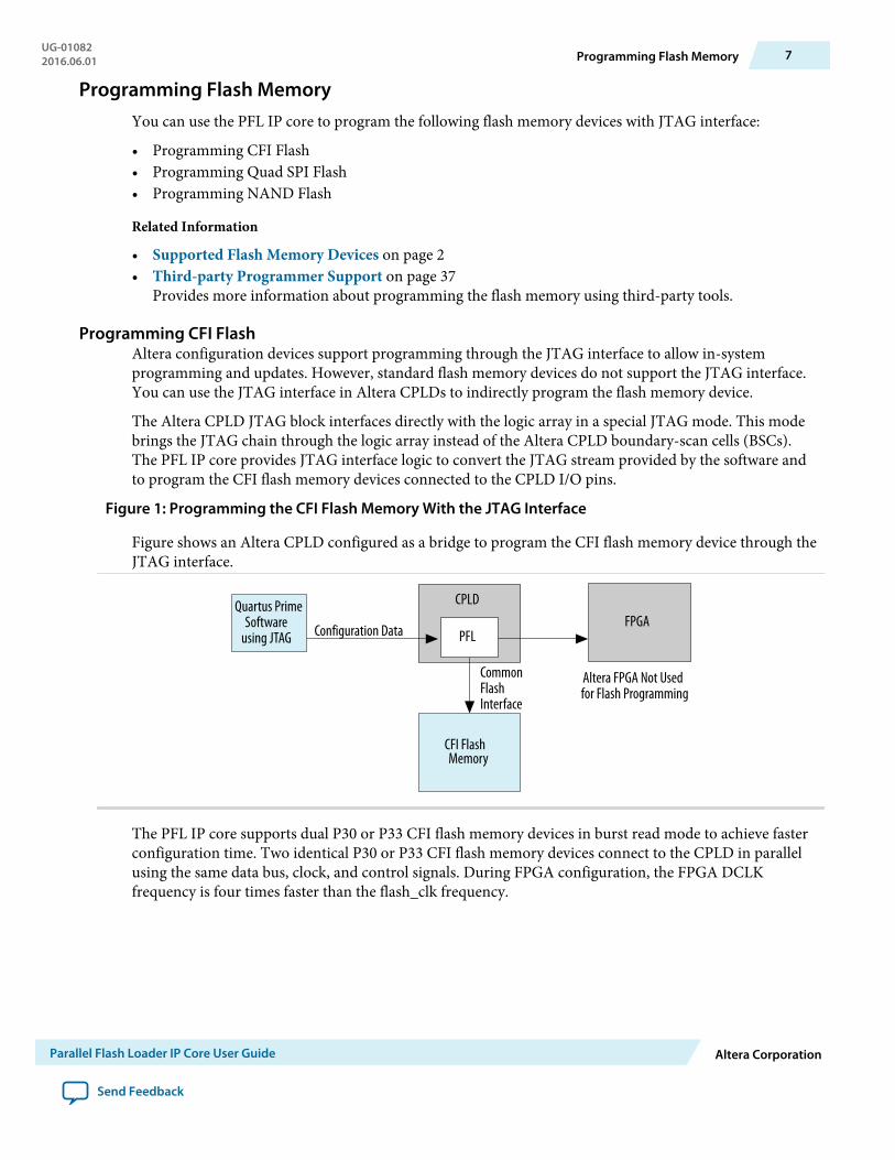
Figure 1: Programming the CFI Flash Memory With the JTAG Interface
Figure shows an Altera CPLD configured as a bridge to program the CFI flash memory device through theJTAG interface.
CPLD
CFI FlashMemory
FPGAConfiguration Data
CommonFlashInterface
PFL
Quartus PrimeSoftware
using JTAG
Altera FPGA Not Usedfor Flash Programming
The PFL IP core supports dual P30 or P33 CFI flash memory devices in burst read mode to achieve fasterconfiguration time. Two identical P30 or P33 CFI flash memory devices connect to the CPLD in parallelusing the same data bus, clock, and control signals. During FPGA configuration, the FPGA DCLKfrequency is four times faster than the flash_clk frequency.
UG-010822016.06.01 Programming Flash Memory 7
Parallel Flash Loader IP Core User Guide Altera Corporation
Send Feedback
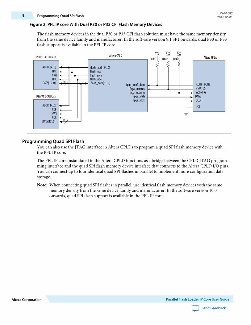
Figure 2: PFL IP core With Dual P30 or P33 CFI Flash Memory Devices
The flash memory devices in the dual P30 or P33 CFI flash solution must have the same memory densityfrom the same device family and manufacturer. In the software version 9.1 SP1 onwards, dual P30 or P33flash support is available in the PFL IP core.
VCC VCC VCCP30/P33 CFI Flash Altera CPLD Altera FPGA
P30/P33 CFI Flash
16
16
10kΩ 10kΩ 10kΩ
ADDR[24..0]NCENWENOE
DATA[15..0]
ADDR[24..0]NCENWENOE
DATA[15..0]
flash_addr[24..0]flash_nceflash_nweflash_noeflash_data[31..0] fpga_conf_done
fpga_nstatusfpga_nconfig
fpga_datafpga_dclk
CONF_DONEnSTATUSnCONFIG
DATA
nCE
DCLK
Programming Quad SPI FlashYou can also use the JTAG interface in Altera CPLDs to program a quad SPI flash memory device withthe PFL IP core.
The PFL IP core instantiated in the Altera CPLD functions as a bridge between the CPLD JTAG program‐ming interface and the quad SPI flash memory device interface that connects to the Altera CPLD I/O pins.You can connect up to four identical quad SPI flashes in parallel to implement more configuration datastorage.
Note: When connecting quad SPI flashes in parallel, use identical flash memory devices with the samememory density from the same device family and manufacturer. In the software version 10.0onwards, quad SPI flash support is available in the PFL IP core.
8 Programming Quad SPI FlashUG-01082
2016.06.01
Altera Corporation Parallel Flash Loader IP Core User Guide
Send Feedback

Figure 3: Programming Quad SPI Flash Memory Devices With the CPLD JTAG Interface
Figure shows an Altera CPLD functioning as a bridge to program the quad SPI flash memory devicethrough the JTAG interface. The PFL IP core supports multiple quad SPI flash programming of up to fourdevices.
VCC VCC VCCQuad SPI Flash Altera CPLD
Altera FPGA
10kΩ 10kΩ 10kΩflash_sck
flash_io0flash_io1flash_io2flash_io3
flash_sck[3..0]
flash_io0[3..0]flash_io1[3..0]flash_io2[3..0]flash_io3[3..0] fpga_conf_done
fpga_nstatusfpga_nconfig
fpga_datafpga_dclk
CONF_DONEnSTATUSnCONFIGDATA
nCE
DCLK
flash_ncs flash_ncs[3..0]
Quad SPI Flash
flash_sck
flash_io0flash_io1flash_io2flash_io3
flash_ncs
Quad SPI Flash
flash_sck
flash_io0flash_io1flash_io2flash_io3
flash_ncs
Quad SPI Flash
flash_sck
flash_io0flash_io1flash_io2flash_io3
flash_ncs
Related InformationSupported Flash Memory Devices on page 2
Programming NAND FlashYou can use the JTAG interface in Altera CPLDs to program the NAND flash memory device with thePFL IP core. The NAND flash memory device is a simpler device that has faster erase and write speed withhigher memory density in comparison with the CFI flash.
You can use the JTAG interface in Altera CPLDs to indirectly program the flash memory device. TheCPLD JTAG block interfaces directly with the logic array in a special JTAG mode. This mode brings theJTAG chain through the logic array instead of the Altera CPLD BSCs. The PFL IP core provides JTAGinterface logic to convert the JTAG stream from the Quartus® Primesoftware and to program the NANDflash memory device that connects to the CPLD I/O pins.
UG-010822016.06.01 Programming NAND Flash 9
Parallel Flash Loader IP Core User Guide Altera Corporation
Send Feedback
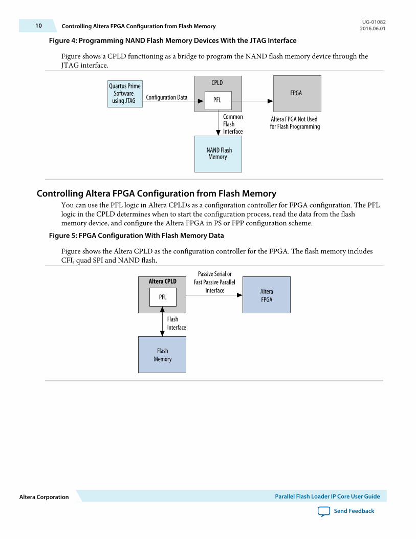
Figure 4: Programming NAND Flash Memory Devices With the JTAG Interface
Figure shows a CPLD functioning as a bridge to program the NAND flash memory device through theJTAG interface.
CPLD
NAND FlashMemory
FPGAConfiguration Data
CommonFlashInterface
PFL
Quartus PrimeSoftware
using JTAG
Altera FPGA Not Usedfor Flash Programming
Controlling Altera FPGA Configuration from Flash MemoryYou can use the PFL logic in Altera CPLDs as a configuration controller for FPGA configuration. The PFLlogic in the CPLD determines when to start the configuration process, read the data from the flashmemory device, and configure the Altera FPGA in PS or FPP configuration scheme.
Figure 5: FPGA Configuration With Flash Memory Data
Figure shows the Altera CPLD as the configuration controller for the FPGA. The flash memory includesCFI, quad SPI and NAND flash.
Altera CPLD
FlashMemory
AlteraFPGA
FlashInterface
PFL
Passive Serial orFast Passive Parallel
Interface
10 Controlling Altera FPGA Configuration from Flash MemoryUG-01082
2016.06.01
Altera Corporation Parallel Flash Loader IP Core User Guide
Send Feedback

You can use the PFL IP core to either program the flash memory devices, configure your FPGA, or both;however, to perform both functions, create separate PFL functions if any of the following conditions applyto your design:
• You want to use fewer LEs.• You modify the flash data infrequently.• You have JTAG or In-System Programming (ISP) access to the Altera CPLD.• You want to program the flash memory device with non-Altera data. For example, the flash memory
device contains initialization storage for an ASSP. You can use the PFL IP core to program the flashmemory device with the initialization data and also create your own design source code to implementthe read and initialization control with the CPLD logic.
Creating Separate PFL Functions
To create separate PFL functions, follow these steps:
1. To create a PFL instantiation, select Flash Programming Only mode.2. Assign the pins appropriately.3. Compile and generate a .pof for the flash memory device. Ensure that you tri-state all unused I/O pins.4. To create another PFL instantiation, select Configuration Control Only mode.5. Instantiate this configuration controller into your production design.6. Whenever you must program the flash memory device, program the CPLD with the flash memory
device .pof and update the flash memory device contents.7. Reprogram the CPLD with the production design .pof that includes the configuration controller.
Note: All unused pins are set to ground by default. When programming the configuration flash memorydevice through the CPLD JTAG pins, you must tri-state the FPGA configuration pins common tothe CPLD and the configuration flash memory device. You can use thepfl_flash_access_request and pfl_flash_access_granted signals of the PFL block to tri-statethe correct FPGA configuration pins.
Related Information
• Mapping PFL and Flash Address on page 11• Implementing Page in the Flash .pof on page 13• Using Enhanced Bitstream Compression and Decompression on page 16• Using Remote System Upgrade on page 18
Mapping PFL and Flash AddressThe address connections between the PFL IP core and the flash memory device vary depending on theflash memory device vendor and data bus width.
UG-010822016.06.01 Mapping PFL and Flash Address 11
Parallel Flash Loader IP Core User Guide Altera Corporation
Send Feedback

Figure 6: Micron J3 Flash Memory in 8-Bit Mode
The address connection between the PFL IP core and the flash memory device are the same.
232221---210
PFLaddress: 24 bits
232221---210
Flash Memoryaddress: 24 bits
Figure 7: Micron J3, P30, and P33 Flash Memories in 16-Bit Mode
The flash memory addresses in Micron J3, P30, and P33 16-bit flash memory shift one bit down incomparison with the flash addresses in the PFL IP core. The flash address in the Micron J3, P30, and P33flash memory starts from bit 1 instead of bit 0.
222120---210
PFLaddress: 23 bits
232221---321
Flash Memoryaddress: 23 bits
Figure 8: Spansion and Micron M28, M29 Flash Memory in 8-Bit Mode
The flash memory addresses in Spansion 8-bit flash shifts one bit up. Address bit 0 of the PFL IP coreconnects to data pin D15 of the flash memory.
232221---210
PFLaddress: 24 bits
222120---10
D15
Flash Memoryaddress: 24 bits
12 Mapping PFL and Flash AddressUG-01082
2016.06.01
Altera Corporation Parallel Flash Loader IP Core User Guide
Send Feedback
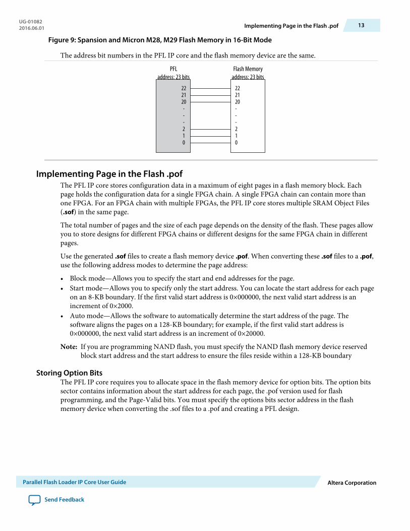
Figure 9: Spansion and Micron M28, M29 Flash Memory in 16-Bit Mode
The address bit numbers in the PFL IP core and the flash memory device are the same.
222120---210
PFLaddress: 23 bits
222120---210
Flash Memoryaddress: 23 bits
Implementing Page in the Flash .pofThe PFL IP core stores configuration data in a maximum of eight pages in a flash memory block. Eachpage holds the configuration data for a single FPGA chain. A single FPGA chain can contain more thanone FPGA. For an FPGA chain with multiple FPGAs, the PFL IP core stores multiple SRAM Object Files(.sof) in the same page.
The total number of pages and the size of each page depends on the density of the flash. These pages allowyou to store designs for different FPGA chains or different designs for the same FPGA chain in differentpages.
Use the generated .sof files to create a flash memory device .pof. When converting these .sof files to a .pof,use the following address modes to determine the page address:
• Block mode—Allows you to specify the start and end addresses for the page.• Start mode—Allows you to specify only the start address. You can locate the start address for each page
on an 8-KB boundary. If the first valid start address is 0×000000, the next valid start address is anincrement of 0×2000.
• Auto mode—Allows the software to automatically determine the start address of the page. The software aligns the pages on a 128-KB boundary; for example, if the first valid start address is0×000000, the next valid start address is an increment of 0×20000.
Note: If you are programming NAND flash, you must specify the NAND flash memory device reservedblock start address and the start address to ensure the files reside within a 128-KB boundary
Storing Option BitsThe PFL IP core requires you to allocate space in the flash memory device for option bits. The option bitssector contains information about the start address for each page, the .pof version used for flashprogramming, and the Page-Valid bits. You must specify the options bits sector address in the flashmemory device when converting the .sof files to a .pof and creating a PFL design.
UG-010822016.06.01 Implementing Page in the Flash .pof 13
Parallel Flash Loader IP Core User Guide Altera Corporation
Send Feedback

Table 4: Option Bits Sector Format
Offset address 0x80 stores the .pof version required for programming flash memory. This .pof version applies toall eight pages of the configuration data. The PFL IP core requires the .pof version to perform a successful FPGAconfiguration process.
Sector Offset Value
0x00–0x03 Page 0 start address0x04–0x07 Page 1 start address0x08–0x0B Page 2 start address0x0C–0x0F Page 3 start address0x10–0x13 Page 4 start address0x14–0x17 Page 5 start address0x18–0x1B Page 6 start address0x1C–0x1F Page 7 start address0x20–0x7F Reserved0x80(4) .pof version
0x81–0xFF Reserved
The Convert Programming File tool generates the information for the .pof version when you convertthe .sof files to .pof files.
The value for the .pof version generated by the Quartus II software version 7.1 onwards is 0x03. However,if you turn on the enhanced bitstream-compression feature, the value for the .pof version is 0x04.
Caution: Do not overwrite any information in the option bits sector to prevent the PFL IP core frommalfunctioning, and always store the option bits in unused addresses in the flash memorydevice.
(4) .pof version occupies only one byte in the option bits sector.
14 Storing Option BitsUG-01082
2016.06.01
Altera Corporation Parallel Flash Loader IP Core User Guide
Send Feedback
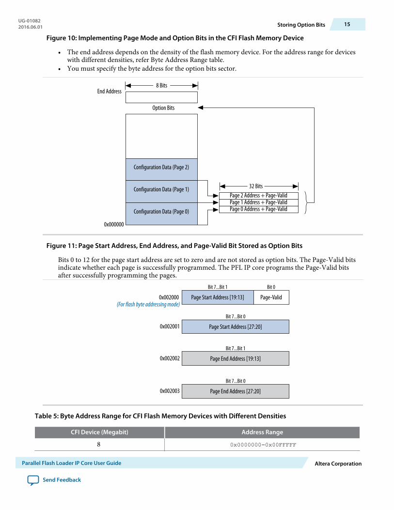
Figure 10: Implementing Page Mode and Option Bits in the CFI Flash Memory Device
• The end address depends on the density of the flash memory device. For the address range for deviceswith different densities, refer Byte Address Range table.
• You must specify the byte address for the option bits sector.
Option Bits
Configuration Data (Page 2)
Configuration Data (Page 1)
Configuration Data (Page 0)
Page 2 Address + Page-ValidPage 1 Address + Page-ValidPage 0 Address + Page-Valid
End Address
0x000000
8 Bits
32 Bits
Figure 11: Page Start Address, End Address, and Page-Valid Bit Stored as Option Bits
Bits 0 to 12 for the page start address are set to zero and are not stored as option bits. The Page-Valid bitsindicate whether each page is successfully programmed. The PFL IP core programs the Page-Valid bitsafter successfully programming the pages.
Page Start Address [19:13] Page-Valid
Bit 7...Bit 1 Bit 0
Page Start Address [27:20]
Bit 7...Bit 0
0x002000
0x002001
Page End Address [19:13]
Bit 7...Bit 1
0x002002
Page End Address [27:20]
Bit 7...Bit 0
0x002003
(For flash byte addressing mode)
Table 5: Byte Address Range for CFI Flash Memory Devices with Different Densities
CFI Device (Megabit) Address Range
8 0x0000000–0x00FFFFF
UG-010822016.06.01 Storing Option Bits 15
Parallel Flash Loader IP Core User Guide Altera Corporation
Send Feedback

CFI Device (Megabit) Address Range
16 0x0000000–0x01FFFFF32 0x0000000–0x03FFFFF64 0x0000000–0x07FFFFF
128 0x0000000–0x0FFFFFF256 0x0000000–0x1FFFFFF512 0x0000000–0x3FFFFFF
1024 0x0000000–0x7FFFFFF
Using Enhanced Bitstream Compression and DecompressionThe enhanced bitstream compression and decompression feature in the PFL IP core reduces the size ofthe configuration file in the flash memory device. On average, you can reduce the file size by as much as50% depending on the designs. When you turn on the enhanced bitstream compression feature, the PFLIP core disables data encryption.
Table 6: Comparison Between Typical, Enhanced, and Double Compression
FPGA Configuration Typical BitstreamCompression Feature
Enhanced BitstreamCompression Feature
Double CompressionTechnique
FPGA on-chip bitstreamdecompression enabled
Yes No Yes
PFL enhanced bitstreamdecompression enabled
No Yes Yes
Typical configuration file sizereduction
35%–55% 45%–75% 40%–60%
PS configuration time Moderate(5) Slow Moderate(5)
FPP configuration time Fast(6) Very fast(7) Not supported
Note: When using the PFL with compression, set the device MSEL pins set for compression ordecompression. When generating or converting a programming file, you can enable compression.In the first few bytes during the generation of the programming file (with compression enabled), abit set notifies the PFL that the incoming files is a compressed file. The ×4 DCLK-to-data arehandled automatically in the PFL.
Note: For more information about the typical data compression feature, refer to the Configuration DataDecompression section in the configuration chapter of the relevant device handbook.
(5) The FPGA receives compressed bitstream which decreases the duration to transmit the bitstream to theFPGA.
(6) For FPP with on-chip bitstream decompression enabled, the DCLK frequency is ×2, ×4, or ×8 the data rate,depending on the device. You can check the relationship of the DCLK and data rate in the FPPConfiguration section in the configuration chapter of the respective device handbook.
(7) For FPP with enhanced bitstream decompression enabled, the DCLK frequency is ×1 the data rate.
16 Using Enhanced Bitstream Compression and DecompressionUG-01082
2016.06.01
Altera Corporation Parallel Flash Loader IP Core User Guide
Send Feedback
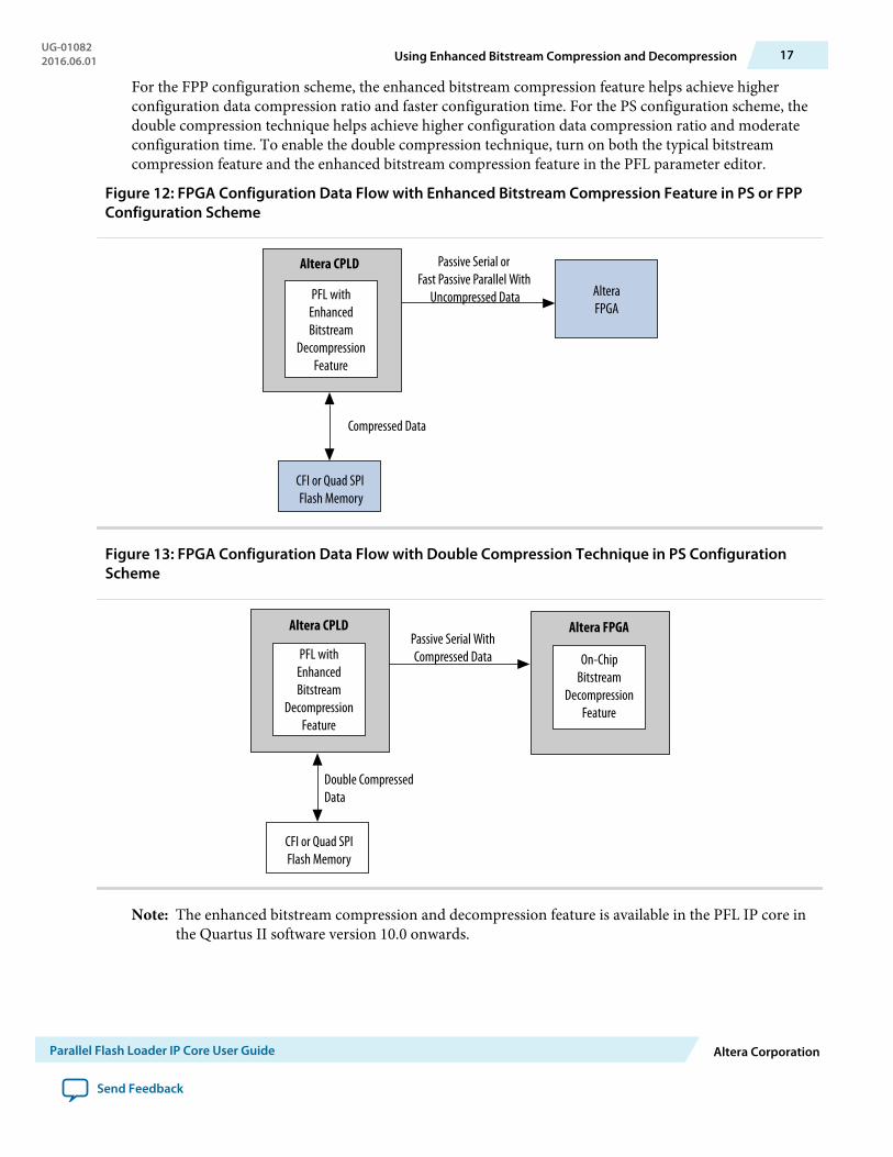
For the FPP configuration scheme, the enhanced bitstream compression feature helps achieve higherconfiguration data compression ratio and faster configuration time. For the PS configuration scheme, thedouble compression technique helps achieve higher configuration data compression ratio and moderateconfiguration time. To enable the double compression technique, turn on both the typical bitstreamcompression feature and the enhanced bitstream compression feature in the PFL parameter editor.
Figure 12: FPGA Configuration Data Flow with Enhanced Bitstream Compression Feature in PS or FPPConfiguration Scheme
Altera CPLD
CFI or Quad SPI Flash Memory
AlteraFPGA
PFL withEnhancedBitstream
DecompressionFeature
Compressed Data
Passive Serial or Fast Passive Parallel With
Uncompressed Data
Figure 13: FPGA Configuration Data Flow with Double Compression Technique in PS ConfigurationScheme
Altera CPLD
CFI or Quad SPIFlash Memory
PFL withEnhancedBitstream
DecompressionFeature
Double Compressed Data
Passive Serial WithCompressed Data
Altera FPGA
On-ChipBitstream
DecompressionFeature
Note: The enhanced bitstream compression and decompression feature is available in the PFL IP core inthe Quartus II software version 10.0 onwards.
UG-010822016.06.01 Using Enhanced Bitstream Compression and Decompression 17
Parallel Flash Loader IP Core User Guide Altera Corporation
Send Feedback

Using Remote System UpgradeWhen you instantiate the PFL IP core in the Altera CPLD for FPP or PS configuration, you can use thefeatures in the PFL IP core to perform remote system upgrade.
You can download a new configuration image from a remote location, store it in the flash memory device,and direct the PFL IP core to trigger an FPGA reconfiguration to load the new configuration image. Youmust store each configuration image as a new page in the flash memory device. The PFL IP core supportsa maximum of eight pages.
When using remote system upgrade, the configuration images are classified as a factory image or asapplication images. A factory image is a user-defined fall-back or safe configuration that performs systemrecovery when unintended errors occur during or after application image configuration. The factoryimage is written to the flash memory device only once by the system manufacturer and you must notmodify or overwrite the factory image. Application images implement user-defined functionality in thetarget FPGA and you can remotely update in the system.
Figure 14: Remote System Upgrade Implementation with the PFL IP Core in FPP and PS ConfigurationScheme
CPLD
CFI FlashMemory
FPGAConfiguration Data
CommonFlashInterface
PFL
Quartus PrimeSoftware
using JTAG
Altera FPGA Not Usedfor Flash Programming
Remote System Upgrade State Machine in the PFL IP CoreAfter FPGA powers up, you have the flexibility to determine whether a factory image or any applicationimage is to be loaded by setting the fpga_pgm[2..0] input pin to the page in which the intendedconfiguration image is stored.
If an error occurs while loading the configuration image, the PFL IP core triggers a reconfiguration toautomatically load the factory image. After the FPGA successfully loads the configuration image, theFPGA enters user mode. After the FPGA enters user mode, you can initiate a reconfiguration to a newpage by following these steps:
1. Set the fpga_pgm[2.0] input pin.2. Release the pfl_nreset to high if the pfl_nreset is asserted to low.3. After four or five clock cycles, pulse the pfl_nreconfigure input pin to low.4. Ensure that all transition is synchronized to pfl_clk.
18 Using Remote System UpgradeUG-01082
2016.06.01
Altera Corporation Parallel Flash Loader IP Core User Guide
Send Feedback

Figure 15: Transitions Between Different Configurations in Remote System Upgrade
• The remote system upgrade feature in the PFL IP core does not restrict the factory image to page 0, butallows the factory image to be located on other pages in the flash.
• You can load the FPGA with either a factory image or any application image after power up,depending on the fpga_pgm[2..0] setting.
Application 1Configuration
Power-up
FactoryConfiguration
Application nConfiguration
fpga_pgm[2..0] is set tofactory page
Set fpga_pgm[2..0] to intended page and pulsepfl_nreconfig
fpga_pgm[2..0] is set toapplication 1 page
Configuration Error
Configuration Error
Configuration Error
fpga_pgm[2..0] is set toapplication n page
Set fpga_pgm[2..0] to intended page and pulsepfl_nreconfig
Set fpga_pgm[2..0] to intended page and pulsepfl_nreconfig
Note: The PFL IP core can implement a Last Revision First programming order. The application image isupdated with remote system upgrade capabilities. If a flash programming error causes the FPGAconfiguration to fail, the FPGA is reconfigured from the factory image address. A system shippedfrom the factory has the same configuration file at the application image address and the factory
UG-010822016.06.01 Remote System Upgrade State Machine in the PFL IP Core 19
Parallel Flash Loader IP Core User Guide Altera Corporation
Send Feedback

image address. Altera recommends that you write-protect the factory image blocks in the flashmemory device.
Implementing Remote System Upgrade with the PFL IP CoreYou can achieve the remote system upgrade capabilities with the PFL IP core by controlling thefpga_pgm[2..0] and the pfl_nreconfigure ports.
To control the fpga_pgm[2..0] and the pfl_nreconfigure ports, user-defined logic must perform thefollowing capabilities:
• After FPGA power up, user logic sets the fpga_pgm[2..0] ports to specify which page of configurationimage is to be loaded from the flash.
• After the remote host completes the new image update to the flash, user logic triggers a reconfigura‐tion by pulling the pfl_nreconfigure pin low and setting the fpga_pgm[2..0] to the page in whichthe new image is located. The pfl_nreconfigure signal pulsed low for greater than one pfl_clkcycle.
• If you have enabled the user watchdog timer, user logic can monitor the pfl_watchdog_error port todetect any occurrence of watchdog time-out error. If the pfl_watchdog_error pin is asserted high,this indicates watchdog time-out error. You can use the user logic to set the fpga_pgm[2..0] and pullthe pfl_nreconfigure port low to initiate FPGA reconfiguration. The recovery page to be loadedfrom the flash memory device after watchdog timer error depends on the fpga_pgm[2..0] setting.
Figure 16: Implementation of Remote System Upgrade with the PFL IP Core
FlashWatchdogtimer reset
circuitry
Altera FPGA
Imageupdatecircuitry
Remote Host
PFL
Watchdog timer reset
User logic
FPP or PSconfiguration
pfl_nreconfigure fpga_pgm[2..0]
Altera CPLD
User Watchdog TimerThe user watchdog timer prevents faulty configuration from stalling the device indefinitely. The systemuses the timer to detect functional errors after a configuration image is successfully loaded into the FPGA.
The user watchdog timer is a time counter that runs at the pfl_clk frequency. The timer beginscounting after the FPGA enters user mode and continues until the timer reaches the watchdog time out
20 Implementing Remote System Upgrade with the PFL IP CoreUG-01082
2016.06.01
Altera Corporation Parallel Flash Loader IP Core User Guide
Send Feedback

period. You must periodically reset this timer by asserting the pfl_reset_watchdog pin before thewatchdog time-out period. If the timer does not reset before the watchdog time-out period, the PFL IPcore detects watchdog time-out error and initiates a reconfiguration to load the factory image.
Instantiate the watchdog timer reset circuitry in the configuration image loaded into the FPGA. Connectone output signal from the reset circuitry to the pfl_reset_watchdog pin of the PFL in the CPLD toperiodically send a reset signal to the user watchdog timer. To reset the watchdog timer correctly, hold thepfl_reset_watchdog pin high or low for at least two pfl_clk cycles.
Note: The user watchdog timer feature for remote system upgrade is available in the PFL IP core in theQuartus II software version 10.0 onwards.
Using the PFL IP CoreThis section describes the procedures on how to use the PFL IP core.
Figure 17: Process for Using the PFL IP Core
Figure shows the process for using the PFL IP core, using MAX II as an example.
Create a new MAX II design, instantiate the PFL Megafunction in
the MAX II design, and createPin Assignments
Add the MAX II .pof to the Quartus Prime Programmer
Add the flash .pof in the Quartus Prime Programmer
Program the MAX II and Flash Devices
MAX II configures the FPGA with theconfiguration data from the Flash Device
Compile andobtain the
FPGA .sof(s)
Convert to .pof for the
TargetedFlash
Compileand obtain
MAX II.pof
Add the .sof(s) for conversion to .pof
Create new FPGAdesigns
Create the optional Jam programming file
UG-010822016.06.01 Using the PFL IP Core 21
Parallel Flash Loader IP Core User Guide Altera Corporation
Send Feedback

Related InformationAN478: Using FPGA-Based Parallel Flash Loader with the Quartus II SoftwareProvides more information about using the FPGA-based PFL IP core to program a flash memory device.
Converting .sof Files to a .pofTo generate a programming file with different compression features, you must convert the .sof files toa .pof.
To convert the .sof files to a .pof, follow these steps:
1. On the File menu, click Convert Programming Files.2. For Programming file type, specify Programmer Object File (.pof) and name the file.3. For Configuration device, select the CFI or NAND flash memory device with the correct density. For
example, CFI_32Mb is a CFI device with 32-Megabit (Mb) capacity.4. To add the configuration data, under Input files to convert, select SOF Data.5. Click Add File and browse to the .sof files you want to add.
You can place more than one .sof in the same page if you intend to configure a chain of FPGAs. Theorder of the .sof files must follow the order of the devices in the chain.If you want to store the data from other .sof files in a different page, click Add SOF page. Add the .soffiles to the new page.
6. Select SOF Data and click Properties to set the page number and name. Under Address mode forselected pages, select Auto to let the Quartus Prime software automatically set the start address forthat page. Select Block to specify the start and end addresses, or select Start to specify the start addressonly.
7. Click OK.8. You can also store Hexadecimal (Intel-Format) File (.hex) user data in the flash memory device:
a. In the Input files to convert sub-window of the Convert Programming Files window, select AddHex Data.
b. In the Add Hex Data dialog box, select either absolute or relative addressing mode.
• If you select absolute addressing mode, the data in the .hex is programmed in the flash memorydevice at the exact same address location listed in the .hex.
• If you select relative addressing mode, specify a start address.
The data in the .hex is programmed into the flash memory device with the specific start address, andthe differences between the addresses are kept. If no address is specified, the software selects anaddress.
Note: You can also add other non-configuration data to the .pof by selecting the .hex that containsyour data when creating the flash memory device .pof.
9. Click Options to specify the start address to store the option bits. This start address must be identicalto the address you specify when creating the PFL IP core. Ensure that the option bits sector does notoverlap with the configuration data pages and that the start address resides on an 8-KB boundary.
10.If you are using a NAND flash memory device, specify the reserved block start address and the startaddress (including the option bits) within a 128-KB boundary. To specify the address, in the File/Dataarea column, select NAND flash Reserved Block and click Properties.
11.To generate programming files with either the typical or enhanced bitstream compression feature, orboth, perform one of the following steps:
22 Converting .sof Files to a .pofUG-01082
2016.06.01
Altera Corporation Parallel Flash Loader IP Core User Guide
Send Feedback
• Typical bitstream compression feature
1. Select .sof under SOF Data.2. Click Properties, and then turn on the Compression option.3. Click OK.
• Enhanced bitstream compression feature
1. In the Options dialog box, turn on the Enable enhanced bitstream-compression whenavailable option.
2. Click OK.• Double compression technique
• Perform all the steps for the typical bitstream compression and enhanced bitstream compressionfeatures listed above.
Note: For more information about the compression feature in the PFL IP core, refer to “UsingEnhanced Bitstream Compression and Decompression”.
12.To generate programming files with encrypted data, select .sof under SOF Data and click Properties.Turn on the Generate encrypted bitstream check box.
13.Click OK to create the .pof.
Related InformationUsing Enhanced Bitstream Compression and Decompression on page 16
Constraining PFL TimingThe PFL IP core supports the TimeQuest Timing Analyzer for accurate timing analysis on the Altera IPcores. To perform timing analysis, you must define the clock characteristics, external path delays, andtiming exceptions for the PFL input and output ports. This section provides guidelines for defining thisinformation for PFL input and output ports for use by the TimeQuest analyzer.
Note: The TimeQuest analyzer is a timing analysis tool that validates the timing performance of the logicin the design using industry-standard constraint, analysis, and reporting methodology. For moreinformation about the TimeQuest analyzer, refer to the TimeQuest Timing Analyzer chapter involume 3 of the Handbook.
Note: After you specify the timing constraint settings for the clock signal and for the asynchronous andsynchronous input and output ports in the TimeQuest analyzer, on the Constraints menu, clickWrite SDC File to write all the constraints to a specific System Design Constraints File (.sdc). Afterthe .sdc is written, run full compilation for the PFL design.
Related InformationQuartus Prime TimeQuest Timing Analyzer of Quartus Prime HandbookProvides more information about the TimeQuest analyzer.
Constraining Clock Signal
At any given time, one of the following two clock sources clocks the blocks and modules of the PFL IPcore:
• Clock signals from the pfl_clk ports of the PFL during FPGA configuration• TCK pins of the JTAG programming interface during flash programming
UG-010822016.06.01 Constraining PFL Timing 23
Parallel Flash Loader IP Core User Guide Altera Corporation
Send Feedback

The clock signal on the TCK pins is internally constrained to the maximum frequency supported by theselected JTAG programming hardware. It is not necessary to constrain the clock signal.
You can constrain pfl_clk to the maximum frequency that the PFL IP core supports. You can use thecreate_clock command or the Create Clock dialog box to specify the period and duty cycle of the clockconstraint.
To constrain the pfl_clk signal in the TimeQuest analyzer, follow these steps:
1. Run full compilation for the PFL design. Ensure that the timing analysis tool is set to TimeQuestTiming Analyzer.
2. After full compilation completes, on the Tools menu, select TimeQuest Timing Analyzer to launchthe TimeQuest analyzer window.
3. In the Tasks list, under Diagnostic, click Report Unconstrained Paths to view the list ofunconstrained parts and ports of the PFL design.
4. In the Report list, under Unconstrained Paths, click Clock Summary to view the clock that requiresconstraints. The default setting for all unconstrained clocks is 1 GHz. To constrain the clock signal,right-click the clock name and select Edit Clock Constraint.
5. In the Create Clock dialog box, set the period and the duty cycle of the clock constraint.6. Click Run.
Constraining Synchronous Input and Output PortsThe setup and hold time of synchronous input and output ports is critical to the system designer. Toavoid setup and hold time violations, you can specify the signal delay from the FPGA or the flash memorydevice to the synchronous input and output ports of the PFL IP core. The Fitter places and routes theinput and output registers of the PFL IP core to meet the specified timing constraints.
Note: For more information about the synchronous input and output ports of the PFL IP core, refer toPFL Timing Constraints table.
The signal delay from FPGA or flash memory device to the PFL synchronous input port is specified byset_input_delay. The delay calculation is:
Input delay value = Board delay from FPGA or flash output port to the PFL input port + TCO of the FPGAor flash memory device
The signal delay from PFL synchronous output port to FPGA or flash memory device is specified byset_output_delay. The delay calculation is:
Output delay value = Board delay from the PFL output port to the FPGA or flash input port + TSU ofFPGA or flash device.
Note: TCO is the clock-to-output time from the timing specification in the FPGA, CPLD or flashdatasheet.
24 Constraining Synchronous Input and Output PortsUG-01082
2016.06.01
Altera Corporation Parallel Flash Loader IP Core User Guide
Send Feedback

To constrain the synchronous input and output signals in the TimeQuest analyzer, follow these steps:
1. Run full compilation for the PFL design. Ensure that the timing analysis tool is set to TimeQuestTiming Analyzer.
2. After full compilation completes, on the Tools menu, select TimeQuest Timing Analyzer to launchthe TimeQuest analyzer window.
3. In the Tasks list, under Diagnostic, click Report Unconstrained Paths to view the list ofunconstrained parts and ports of the PFL design.
4. In the Report list, under the Unconstrained Paths category, select Setup Analysis, and then clickUnconstrained Input Port Paths.
5. Right-click each synchronous input or output port in the From list or To list and selectset_input_delay for the input port or set_output_delay for the output port, then specify the inputdelay or output delay value.
Related InformationSummary of PFL Timing Constraints on page 25
Constraining Asynchronous Input and Output PortsYou can exclude asynchronous input and output ports from the timing analysis of the PFL IP corebecause the signals on these ports are not synchronous to a IP core clock source. The internal structure ofthe PFL IP core handles the metastability of these asynchronous signals.
To exclude asynchronous input and output ports from the timing analysis, use the set_false_pathcommand to ignore these ports during timing analysis.
Note: After you specify all timing constraint settings for the clock signal, on the Constraints menu, clickWrite SDC File to write all the constraints to a specific .sdc. Then, run full compilation for the PFLdesign again.
Summary of PFL Timing Constraints
Table 7: PFL Timing Constraints
Type Port Constraint Type Delay Value
Input clock pfl_clk create_clock Can be constrained up to themaximum frequency supportedby the PFL IP core.
Input asynchro‐nous
pfl_nreset set_false_path —fpga_pgm set_false_path —
fpga_conf_done set_false_path —fpga_nstatus set_false_path —
pfl_flash_access_granted set_false_path —pfl_nreconfigure set_false_path —
UG-010822016.06.01 Constraining Asynchronous Input and Output Ports 25
Parallel Flash Loader IP Core User Guide Altera Corporation
Send Feedback

Type Port Constraint Type Delay Value
Output asynchro‐nous
fpga_nconfig set_false_path —
pfl_flash_access_request set_false_path —flash_nce set_false_path —flash_nwe set_false_path —flash_noe set_false_path —flash_addr set_false_path —
Bidirectionalsynchronous
flash_data • Normal read mode:
set_false_path
• Burst read mode:
set_input_delay
Burst read mode:
Board delay from flash devicedata pins to CPLD data pins +Tco of flash device.
Output synchro‐nous
fpga_data set_output_delay Board delay + TSU of the FPGAfpga_dclk set_output_delay Board delay from fpga_dclk
pin of the CPLD to DCLK pin ofthe FPGA
Simulating PFL DesignYou can simulate the behavior of the PFL IP core with the ModelSim®-Altera software as it configures anFPGA. This section provides guidelines on the PFL simulation for FPGA configuration.
Note: PFL simulation is based on functional netlist, and does not support gate-level simulation. PFLsimulation does not reflect the true behavior of the hardware. Altera certifies the PFL IP core basedon actual hardware testing, and not through PFL simulation. The PFL simulation only providesprimitive behavioral simulation.
Table 8: Files Required for PFL Simulation in the ModelSim-Altera Software
File/Library Description
.vo or .vho The Verilog HDL or VHDL output file of the PFL IP core.
.sdo The Standard Delay Format Output file (.sdo) of the PFL IP core.
Simulation libraries:
• altera• altera_mf• maxii• maxv
The precompiled library files for Altera IP core primitives and Altera CPLDsin the ModelSim-Altera software.
Test bench Test bench file to establish the interface between the PFL IP core and the flashmemory device.
Flash simulation modelfiles
The simulation model files for the flash memory devices in the PS or FPPconfiguration. For the flash simulation model file for each flash memorydevice, refer to the respective flash memory device manufacturer.
26 Simulating PFL DesignUG-01082
2016.06.01
Altera Corporation Parallel Flash Loader IP Core User Guide
Send Feedback

Related Information
• ModelSim-Altera Software SupportProvides more information about simulation setup in ModelSim-Altera software.
• Altera Knowledge CenterProvides more information about known PFL simulation issues.
Creating a Test Bench File for PFL SimulationYou can use a test bench file to establish the interface between the PFL IP core and the flash memorydevice. You must map the input and output ports of the PFL IP core to the appropriate data or addressbus, and to the control signals of the flash.
To perform the signal mapping, you must include the PFL primitive block and the flash primitive block inthe test bench. The primitive blocks contain the input and output ports of the device. You can obtain theflash primitive blocks from the simulation model files provided by the flash memory device manufacturer.
To establish the connection between the PFL IP core and the flash memory device, you must connect theflash data bus, the flash address bus, and the flash control signals from the PFL primitive block to theappropriate ports of the flash primitive block.
Example 1: PFL Primitive Block
pfl pfl_inst ( .fpga_pgm(<fpga_pgm source>), .pfl_clk(<pfl clock source>), .pfl_flash_access_granted(<pfl_flash_access_granted source>), .pfl_flash_access_request(<pfl_flash_access_granted destination>), .pfl_nreconfigure(<pfl_nreconfigure source>), .pfl_nreset(<pfl_nreset source>), .flash_addr(<flash address bus destination>), .flash_data(<flash_data bus destination>), .flash_nce(<flash_nce destination>), .flash_noe(<flash_noe destination>), .flash_nreset(<flash_nreset destination>), .flash_nwe(<flash_nwe destination>), .fpga_conf_done(<fpga_conf_done source>), .fpga_nstatus(<fpga_nstatus source>), .fpga_data(<fpga_data destination>), .fpga_dclk(<fpga_dclk destination>), .fpga_nconfig(<fpga_nconfig destination>), );
Note: For more information about the flash simulation model files, contact the flash memory devicemanufacturer.
Performing PFL Simulation in the ModelSim-Altera SoftwareTo perform PFL simulation in the ModelSim-Altera software, you must specify the .sdo or load theModelSim precompiled libraries listed in Files Required for PFL Simulation in the ModelSim-AlteraSoftware table. Alternatively, you can generate the .vo, .sdo and Modelsim precompiled libraries throughNativeLink feature in Quartus Prime.
UG-010822016.06.01 Creating a Test Bench File for PFL Simulation 27
Parallel Flash Loader IP Core User Guide Altera Corporation
Send Feedback

To set up the simulation using NativeLink and perform ModelSim simulation, follow these steps:
1. On the Assignments menu, click Settings to open the Settings dialog box and then under EDA ToolSettings, click Simulation.
2. Verify that ModelSim-Altera is selected in the Tool name field and click OK.3. To run simulation right after design compilation, turn on theRun gate-level simulation automatically
after compilation option.4. Specify Format for output netlist, Time scale, and Output directory.5. Under NativeLink settings, select Compile test bench then click Test Benches.6. In the Test Bench dialog box appears, click New. Fill in the settings, insert simulation model files for
the flash memory devices and test bench.Figure 18: Test Bench Settings
7. After settings was done, compile the design and the simulation will start automatically.
Related InformationSimulating PFL Design on page 26
28 Performing PFL Simulation in the ModelSim-Altera SoftwareUG-01082
2016.06.01
Altera Corporation Parallel Flash Loader IP Core User Guide
Send Feedback

Performing PFL Simulation for FPGA ConfigurationBefore beginning the FPGA configuration, the PFL IP core reads the option bits stored in the option bitssector to obtain information about the .pof version used for flash programming, the start and end addressof each page of the configuration image stored in the flash, and the Page-Valid bit.
In this simulation example, the start and end addresses of the option bits sector are 0×800000 and0×800080, respectively. The PFL IP core first reads from the final address, which is 0×800080, to obtainthe .pof version information. Because fpga_pgm[2..0] is set to 000, the PFL IP core reads from address0×800000 to address 0×800003 to get the start and end address of page 0 and the Page-Valid bit. The LSBin address 0×800000 is the Page-Valid bit.
The Page-Valid bit must be 0 for the PFL IP core to proceed with FPGA configuration. While the PFL IPcore reads from the flash, it asserts the active-low flash_nce and flash_noe signals, and asserts theactive-high pfl_flash_access_request signal.
Note: Before you perform the device configuration simulation, ensure that the PFL IP core receives thecorrect option bits address and associated values to guarantee correct simulation output.
Figure 19: Simulation Before Configuration
Figure shows the simulation when the PFL IP core reads the option bits from the flash memory devicebefore configuration starts.
After reading the option bits for page 0, the PFL IP core waits for a period of time before the configurationstarts. The flash_data remains at 0×ZZ within this period. Configuration starts when the fpga_dclkstarts to toggle. During configuration, the PFL IP core asserts the flash_nce and flash_noe signals low,and the pfl_flash_access_request signal high.
UG-010822016.06.01 Performing PFL Simulation for FPGA Configuration 29
Parallel Flash Loader IP Core User Guide Altera Corporation
Send Feedback

Figure 20: Simulation When FPGA Configuration Starts
The FPGA configuration continues until the fpga_conf_done signal is asserted high, which indicates theconfiguration is complete. After the configuration process completes, the PFL IP core pulls the flash_nceand flash_noe signals high and the pfl_flash_access_request signal low to indicate the configurationdata is no longer being read from the flash memory device.
Programming Altera CPLDs and Flash Memory DevicesUsing the Programmer, you can program Altera CPLDs and flash memory device in a single step orseparate steps.
To program both in a single step, first program the CPLD, then the flash memory device. Follow thesesteps:
1. Open the Programmer window and click Add File to add the .pof for the CPLD.2. Right-click the CPLD .pof and click Attach Flash Device.3. In the Flash Device menu, select the density of the flash memory device to be programmed.4. Right-click the necessary flash memory device density and click Change File.5. Select the .pof generated for the flash memory device. The .pof for the flash memory device is attached
to the .pof of the CPLD.6. Add other programming files if your chain has other devices.7. Check all the boxes in the Program/Configure column for the new .pof and click Start to program the
CPLD and flash memory device.The Programmer allows you to program, verify, erase, blank-check, or examine the configuration datapage, the user data page, and the option bits sector separately, provided the CPLD contains the PFL IPcore.
30 Programming Altera CPLDs and Flash Memory DevicesUG-01082
2016.06.01
Altera Corporation Parallel Flash Loader IP Core User Guide
Send Feedback

Note: The programmer erases the flash memory device if you select the .pof of the flash memorydevice before programming. To prevent the Programmer from erasing other sectors in the flashmemory device, select only the pages, .hex data, and option bits.
Programming Altera CPLDs and Flash Memory Devices Separately
To program the CPLD and the flash memory devices separately, follow these steps:
1. Open the Programmer window.2. Click Add File. The Add Programming File Window dialog box appears.3. Add the targeted .pof, and click OK.4. Check the boxes under the Program/Configure column of the .pof.5. Click Start to program the CPLD.6. After the programming progress bar reaches 100%, click Auto Detect. For example, if you are using
dual P30 or P33, the programmer window shows a dual P30 or P33 chain in your setup.Alternatively, you can add the flash memory device to the programmer manually. Right-click theCPLD .pof and click Select Flash Device. In the Select Flash Device dialog box, select the device ofyour choice.
7. Right-click the necessary flash memory device density and click Change File.
Note: You must select the density that is equivalent to the sum of the density of two CFI or NANDflash memory devices. For example, if you require two 512-Mb CFI flash memory devices, thenselect CFI 1 Gbit. For more than one quad SPI flash memory device, select the density that isequivalent to the sum of all the density of the quad SPI flash memory devices. For example, afour quad SPI flash memory devices (128 Mb for each device), the total density is equivalent to512 Mb. A .pof with 512-Mb flash density is required to program these quad SPI flash devices.The PFL IP core handles the 512-Mb .pof programming to the four quad SPI flash memorydevices.
8. Select the .pof generated for the flash memory device. The .pof for the flash memory device is attachedto the .pof of the CPLD.
9. Check the boxes under the Program/Configure column for the added .pof and click Start to programthe flash memory devices.
Defining New CFI Flash DeviceThe PFL IP core supports Intel-compatible and AMD-compatible flash memory devices. In addition tothe supported flash memory devices, you can define the new Intel- or AMD-compatible CFI flashmemory device in the PFL-supported flash database using the Define new CFI flash memory devicefeature.
To add a new CFI flash memory device to the database or update a CFI flash device in the database, followthese steps:
1. In the Programmer window, on the Edit menu, select Define New CFI Flash Device. The Define CFIFlash Device window appears. The following table lists the three functions available in the Define CFIFlash Device window.
UG-010822016.06.01 Programming Altera CPLDs and Flash Memory Devices Separately 31
Parallel Flash Loader IP Core User Guide Altera Corporation
Send Feedback

Table 9: Functions of the Define CFI Flash Device Feature
Function Description
New Add new Intel- or AMD-compatible CFI flash memory device into the PFL-supported flash database.
Edit Edit the parameters of the newly added Intel- or AMD-compatible CFI flashmemory device in the PFL-supported flash database.
Remove Remove the newly added Intel- or AMD-compatible CFI flash memory devicefrom the PFL-supported flash database.
2. To add a new CFI flash memory device or edit the parameters of the newly added CFI flash memorydevice, select New or Edit. The New CFI Flash Device dialog box appears.
3. In the New CFI Flash Device dialog box, specify or update the parameters of the new flash memorydevice. You can obtain the values for these parameters from the datasheet of the flash memory devicemanufacturer.
Table 10: Parameter Settings for New CFI Flash Device
Parameter Description
CFI flash device name Define the CFI flash name
CFI flash device ID Specify the CFI flash identifier code
CFI flash manufacturer ID Specify the CFI flash manufacturer identification number
CFI flash extended device ID Specify the CFI flash extended device identifier, onlyapplicable for AMD-compatible CFI flash memory device
Flash device is Intel compatible Turn on the option if the CFI flash is Intel compatible
Typical word programming time Typical word programming time value in µs unit
Maximum word programming time Maximum word programming time value in µs unit
Typical buffer programming time Typical buffer programming time value in µs unit
Maximum buffer programming time Maximum buffer programming time value in µs unit
Note: You must specify either the word programming time parameters, buffer programming timeparameters, or both. Do not leave both programming time parameters with the default value ofzero.
4. Click OK to save the parameter settings.5. After you add, update, or remove the new CFI flash memory device, click OK.
Related InformationSupported Flash Memory Devices on page 2
Programming Multiple Flash Memory DevicesThe PFL IP core supports multiple-flash programming of as many as 16 flash memory devices. Thisfeature allows the PFL IP core to connect to multiple flash memory devices to perform flash programmingsequentially. PFL multiple-flash programming supports both speed and area mode flash programming.
32 Programming Multiple Flash Memory DevicesUG-01082
2016.06.01
Altera Corporation Parallel Flash Loader IP Core User Guide
Send Feedback

For FPGA configuration, use the content in the flash memory device that connects to the nCE[0] pin asconfiguration data.
To use the multiple flash programming feature, follow these steps:
1. Select the number of flash memory devices connected to the CPLD in the PFL IP core parametereditor.
2. Connect the nCE pins of the PFL to the nCE pins of the flash memory device in the block diagram.Compile the design.
3. Click Auto Detect in the programmer. The CPLD appears as the main item, followed by a list of CFIflash memory devices detected as secondary items in the device tree.
4. Attach the flash memory device .pof to each flash memory device.5. Check the boxes in the Programmer for the necessary operation and click Start.
Creating Jam Files for Altera CPLDs and Flash Memory Device ProgrammingTo use .jam files to program the CPLD and flash memory device, follow these steps:
1. Open the Programmer window and click Add File to add the .pof for the CPLD.2. Right-click the CPLD .pof and click Attach Flash Device.3. In the Flash Device menu, select the density of the flash memory device to be programmed.4. Right-click the necessary flash memory device density and click Change File.5. Select the .pof generated for the flash memory device. The .pof for the flash memory device is attached
to the .pof of the CPLD.6. On the File menu, point to Create/Update and click Create JAM, JBC, SVF, or ISF File.7. Enter a name and select the file format (.jam).8. Click OK.
Note: Use the .jam files with the Programmer or quartus_jli executable file.
Related InformationAN425: Using the Command-Line Jam STAPL Solution for Device Programming.Provides more information about the quartus_jli executable.
PFL IP Core In Embedded SystemsThe PFL IP core allows processors, such as the Nios® II processor, to access the flash memory devicewhile programming flash and configuring an FPGA.
The following figure shows how you can use the PFL IP core to program the flash memory device and toconfigure the FPGA with a Nios II processor. The configured Nios II processor uses the non-configura‐tion data stored in the same flash memory device.
UG-010822016.06.01 Creating Jam Files for Altera CPLDs and Flash Memory Device Programming 33
Parallel Flash Loader IP Core User Guide Altera Corporation
Send Feedback

Figure 21: Single-Device Configuration Using the PFL With the Controller
pfl_nresetpfl_flash_access_granted
flash_addrflash_dataflash_nweflash_nceflash_noe
pfl_flash_access_requestfpga_conf_done
fpga_nstatusfpga_nconfigfpga_data
fpga_dclk
nRPnWP
ADDRDATAnWEnCEnOE
WP#/ACCBYTE#
VCC10kΩ
VCC
Altera FPGAAltera CPLDCFI Flash 10kΩ
VCC10kΩVCC VCC
(1)(1)(1)
(2)
Nios II Processor Interface
(3)
(4)
flash_access_grantedext_ram_bus_addrext_ram_bus_datawrite_n_to_ext_flashchip_n_to_ext_flashoutput_n_to_ext_flashWP#/ACCBYTE#
flash_access_request
NC
CONF_DONEnSTATUSnCONFIGDATADCLKnCE nCEO
You must connect the pull-up resistor to a supply that provides an acceptable input signal for the devices. V CC must be high enough to meet the VIH specification of the I/Oon both devices. For example, the Stratix II V IH specification ranges from 1.7 to 3.3 V; therefore, the supply for the pull-up resistor, V CC, must be within 1.7 to 3.3 V to meetthe VIH specification.For PS configuration mode, this is a 1-bit data line. For FPP configuration mode, this is an 8-bit data bus.Do not connect anything to the NC pin (the no connect pin), not even VCC or GND.You can use the Nios II processor in other Altera FPGA, except when you are configuring the FPGA.
(1)
(2)(3)(4)
Figure 22: Relationship Between the Four Sections in the Design Example
CFI FlashMemory
Common FlashInterface
PFL
pfl_flash_access_granted pfl_flash_access_request
Altera FPGAwith
NIOS II Processor
Altera CPLD
You must configure the Altera FPGA with the Nios II processor when you power up the board. You canstore the Nios II processor image in the flash memory device and use the PFL IP core to configure theimage to the Altera FPGA. If you store the Nios II processor image in the same flash memory device you
34 PFL IP Core In Embedded SystemsUG-01082
2016.06.01
Altera Corporation Parallel Flash Loader IP Core User Guide
Send Feedback

intend to program, do not overwrite the Nios II processor image when you program the flash memorydevice with other user data.
If you do not want to store the image in the flash memory device, you can store the Nios II image in adifferent storage device, for example an enhanced configuration (EPC) device or an erasable program‐mable configurable serial (EPCS) memory.
In Relationship Between the Four Sections in the Design Example figure above, the Nios II processor andthe PFL IP core share the same bus line to the flash memory device. However, to avoid data contention,the processor and the IP core cannot access or program the flash memory device at the same time. Toensure that only one controller (the processor or the IP core), is accessing the flash memory device at anygiven time, you must tri-state all output pins from one controller to the flash memory device, while theother controller is accessing the flash memory device using the pfl_flash_access_request andpfl_flash_access_granted pins in the PFL IP core.
Table 11: PFL Flash Access Pins and Functions
Pin Description
pfl_flash_access_request The PFL IP core drives this pin high to request access to the flashmemory device.
pfl_flash_access_granted The PFL IP core enables the access to the flash memory devicewhenever the PFL IP core receives a high input signal at this pin.
Table 12: pfl_flash_access_request and pfl_flash_access_granted Pins With the Nios II and PFL IP Core
Table lists the methods to use the pfl_flash_access_request and pfl_flash_access_granted pins to ensureboth processors are not accessing the flash memory device at the same time.
Signal Nios II Processor PFL IP Core
High output signal atpfl_flash_access_
request
Tri-state all output pins tothe flash memory device.
Connect all input and output pins to the flashmemory device when the pfl_flash_access_granted pin receives a high input.
Low output signal atpfl_flash_access_
request
Reconnect all pins to theflash memory device.
Tri-state all output pins to the flash memory devicewhen the pfl_flash_access_granted pin receivesa low input.
Note: The Set bus pins to tri-state when not in use option for the PFL IP core disables the PFL IP corewhenever the pfl_flash_access_granted pin is pulled low.
UG-010822016.06.01 PFL IP Core In Embedded Systems 35
Parallel Flash Loader IP Core User Guide Altera Corporation
Send Feedback

Figure 23: Nios II Processor and PFL Accessing the Flash Memory Device Sequence
Nios II processor connectsto the flash device
The PFL megafunction pulls the pfl_flash_access_request pin highto request access to the flash device.
PFL megafunction requestsaccess to flash device
Nios II processor releasesthe flash device
PFL megafunction accessesthe flash device
PFL megafunction releasesthe flash device
By default, the Nios II processor is connected to the flash device. All PFL megafunction output pins are tri-stated.
The Nios II processor tri-states all output pins to the flash device and routesthe output of pfl_flash_access_request to pfl_flash_access _granted.
The PFL megafunction accesses the flash device after receivinga high input at the pfl_flash_access_granted input pin.The pfl_flash_access_request pin stays high as long asthe PFL megafunction is connected to the flash device.
The PFL megafunction pulls the pfl_flash_access_request output pin lowafter accessing the flash device.
Note: Altera recommends that you enable the safe state machine setting to prevent the PFL IP core fromentering an undefined state. To set this option, on the Assignments menu, click Settings. In theSettings dialog box, on the Analysis and Synthesis page, click More Settings, and select safe statemachine.
The Altera CPLD and Nios II processor can each program the CFI flash memory device individually. Toprevent both processors from accessing the CFI flash memory device at the same time, theflash_access_granted and flash_access_request pins of the CPLD and Nios II processor are connectedtogether.
To use other processors or controllers in place of the Nios II processor, ensure that thepfl_flash_access_granted and pfl_flash_access_request pins of the PFL IP core connect to yourprocessor using the method in pfl_flash_access_request and pfl_flash_access_granted Pins Withthe Nios II and PFL IP Core table above.
You must also specify the flash memory device read or write access time for your processor or controller.To avoid data contention when the PFL IP core is accessing the flash memory device, ensure that theoutput pins from your processor are tri-stated when the pfl_flash_access_request signal is high.
Related InformationNios II Processor Reference HandbookProvides more information about the Nios II processor.
36 PFL IP Core In Embedded SystemsUG-01082
2016.06.01
Altera Corporation Parallel Flash Loader IP Core User Guide
Send Feedback

Third-party Programmer SupportYou can program the flash memory using a third-party programmer instead of using Parallel Flash LoaderIP core. To program using third-party programmer, you need to convert the .pof to an .rbf by followingthe steps below:
1. Compile and generate a .pof file for the flash memory device.2. Convert .pof file to .hexout file using the following command:
quartus_cpf -c <pof_file_base_name>.pof <hex_file_base_name>.hexout
3. Convert .hexout file created above to .rbf using the nios2-elf-objcopy command on Nios II CommandShell:
nios2-elf-objcopy –I ihex –O binary <input file>.hexout <output file>.rbf
Related Information
• Programming Flash Memory on page 7• NIOS II Command-Line Tools
Provides more information on the nios2-elf-objcopy command.
Parameters
Table 13: PFL General Parameters
Options Value Description
Operatingmode
• Flash Programming and FPGAConfiguration
• Flash Programming• FPGA Configuration
Specifies the operating mode of flash programmingand FPGA configuration control in one IP core orseparate these functions into individual blocks andfunctionality.
Targetedflash device
• CFI Parallel Flash• Altera Active Serial ×4• Quad SPI Flash• NAND Flash
Specifies the flash memory device connected to thePFL IP core.
Tri-stateflash bus
On or Off Allows the PFL IP core to tri-state all pins interfacingwith the flash memory device when the PFL IP coredoes not require an access to the flash memory.
UG-010822016.06.01 Third-party Programmer Support 37
Parallel Flash Loader IP Core User Guide Altera Corporation
Send Feedback

Table 14: PFL Flash Interface Setting Parameters
Options Value Description
Number offlash devicesused
• CFI Parallel Flash: 1–16• Altera Active Serial ×4: 1, 2, 4,
8• Quad SPI Flash: 1, 2, 4, 8• NAND Flash: 1
Specifies the number of flash memory devicesconnected to the PFL IP core. Allows up to four flashmemory devices.
Largest flashdensity
• CFI Parallel Flash: 8 Mbit–2Gbit
• NAND Flash: 512 Mbit/2 Gbit- Micron(NAND)
• 1 Gbit - Micron (MT29)• Altera Active Serial x4: EPCQ
256 Mbit
Specifies the density of the flash memory device to beprogrammed or used for FPGA configuration. If youhave more than one flash memory device connected tothe PFL IP core, specify the largest flash memorydevice density.
For CFI flash, select the density that is equivalent to thesum of the density of two CFI flashes. For example, ifyou use two 512-Mb CFI flashes, you must select CFI 1Gbit. (Available only if you select CFI Parallel Flashor NAND Flash.)
Flashinterfacedata width
• CFI Parallel Flash: 8, 16, or 32bits
• NAND Flash: 8 bits or 16 bits
Specifies the flash data width in bits. The flash datawidth depends on the flash memory device you use.For multiple flash memory device support, the datawidth must be the same for all connected flash memorydevices.
For CFI flash, select the flash data width that isequivalent to the sum of the data width of two CFIflashes. For example, if you are targeting dual P30 orP33 solution, you must select 32 bits because each CFIflash data width is 16 bits. (Available only if you selectCFI Parallel Flash or NAND Flash.)
User controlflash_
nreset pin
On or Off Creates a flash_nreset pin in the PFL IP core toconnect to the reset pin of the flash memory device. Alow signal resets the flash memory device. In burstmode, this pin is available by default.
When using a Spansion GL flash device, connect thispin to the RESET# pin of the flash device. (Availableonly if you select CFI Parallel Flash.)
Quad SPIflash devicemanufac‐turer
• Macronix• Micron• Spansion
Specifies the device manufacturer of the quad SPI flash.(Available only if you select Quad SPI Flash.)
38 ParametersUG-01082
2016.06.01
Altera Corporation Parallel Flash Loader IP Core User Guide
Send Feedback

Options Value Description
Quad SPIflash devicedensity
8 Mbit–256 Mbit Specifies the density of the quad SPI flash to beprogrammed or used for FPGA configuration.(Available only if you select Quad SPI Flash.)
Byte addressfor reservedblock area
— Specifies the start address of the reserved block area forbad block management.
NAND flash memory may contain bad blocks thatcontain one or more invalid bits. The reserve blocksreplace any bad blocks that the PFL IP core encounters.Altera recommends that you reserve a minimum of 2%of the total block. (Available only if you select NANDFlash.)
On-die ECCsupport
On or Off Enables the support for on-die ECC. Certain NANDflash memory devices has on-die ECC. Allows the PFLIP core to use the on-die ECC of the flash memorydevice.
Turning off this option allows the PFL IP core togenerate its own ECC engine. (Available only if youselect NAND Flash.)
Table 15: PFL Flash Programming Parameters
Options Value Description
Flashprogram‐ming IPoptimization
Area, Speed Specifies the flash programming IP optimization. Ifyou optimize the PFL IP core for speed, the flashprogramming time is shorter but the IP core uses moreLEs. If you optimize the PFL IP core for area, the IPcore uses less LEs, but the flash programming time islonger. (Available only if you select CFI ParallelFlash.)
FIFO size — Specifies the FIFO size if you select Speed for flashprogramming IP optimization. The PFL IP core usesadditional LEs to implement FIFO as temporarystorage for programming data during flash program‐ming. With a larger FIFO size, programming time isshorter. (Available only if you select CFI ParallelFlash.)
Add Block-CRCverificationaccelerationsupport
On or Off Adds a block to accelerate verification. (Available onlyif you select CFI Parallel Flash.)
UG-010822016.06.01 Parameters 39
Parallel Flash Loader IP Core User Guide Altera Corporation
Send Feedback

Table 16: PFL FPGA Configuration Parameters
Options Value Description
Externalclockfrequency
— Specifies the user-supplied clock frequency for the IPcore to configure the FPGA. The clock frequency mustnot exceed two times the maximum clock (DCLK)frequency acceptable by the FPGA for configuration.The PFL IP core can divide the frequency of the inputclock maximum by two.
Flash accesstime
— Specifies the access time of the flash. You can get themaximum access time that a flash memory devicerequires from the flash datasheet. Altera recommendsspecifying a flash access time that is the same as orlonger than the required time.
For CFI parallel flash, the unit is in ns and for NANDflash, the unit is in us. NAND flash uses page instead ofbyte, and requires more access time. This option isdisabled for quad SPI flash.
Option bitsbyte address
— Specifies the start address in which the option bits arestored in the flash memory. The start address mustreside on an 8-KB boundary.
See related for more information about option bits.
FPGAconfigura‐tion scheme
• PS• FPP• FPP ×16 (for Stratix V devices)• FPP ×32(for Stratix V devices)
Select the FPGA configuration scheme. The defaultFPP is FPP ×8. If you are using Stratix V devices, twoadditional FPP mode is available: FPP ×16 and FPP×32.
Configura‐tion failureresponseoptions
Halt, Retry same page, or Retryfrom fixed address
Configuration behavior after configuration failure.
• If you select Halt, the FPGA configuration stopscompletely after failure.
• If you select Retry same page, after failure, the PFLIP core reconfigures the FPGA with data from thesame page of the failure.
• If you select Retry from fixed address, the PFL IPcore reconfigures the FPGA with data from a fixedaddress in the next option field after failure.
Byte addressto retry fromon configu‐ration failure
— If you select Retry from fixed address for configura‐tion failure option, this option specifies the flashaddress for the PFL IP core to read from the reconfigu‐ration for a configuration failure.
40 ParametersUG-01082
2016.06.01
Altera Corporation Parallel Flash Loader IP Core User Guide
Send Feedback
Options Value Description
Includeinput toforcereconfigura‐tion
On or Off Includes an optional reconfiguration input pin (pfl_nreconfigure) to enable a reconfiguration of theFPGA.
Watchdogtimer
On or Off Enables a watchdog timer for remote system upgradesupport. Turning on this option enables the pfl_reset_watchdog input pin and pfl_watchdog_erroroutput pin, and specifies the time period before thewatchdog timer times out. This watchdog timer is atime counter which runs at the pfl_clk frequency.
Time periodbefore thewatchdogtimer timesout
— Specifies the time out period of the watchdog timer.The default time out period is 100 ms
Ratiobetweeninput clockand DCLKoutput clock
1, 2, 4, or 8 Specifies the ratio between the input clock and DCLK.
• Ratio 8 means every eight external clocks to pfl_clk generate one fpga_dclk.
• Ratio 4 means every four external clocks to pfl_clkgenerate one fpga_dclk.
• Ratio 2 means every two external clocks to pfl_clkgenerate one fpga_dclk.
• Ratio 1 means every one external clock to pfl_clkgenerate one fpga_dclk.
Use advanceread mode
• Normal Mode• Intel Burst Mode (P30 or P33)• Spansion Page Mode (GL)• Micron Burst Mode (M58BW)
An option to improve the overall flash access time forthe read process during the FPGA configuration.
• Normal mode—Applicable for all flash memory• Intel Burst mode—Applicable for Micron P30 and
P33 flash memory only. Reduces sequential readaccess time
• Spansion page mode—Applicable for Spansion GLflash memory only
• Micron burst mode—Applicable for MicronM58BW flash memory only
For more information about the read-access modes ofthe flash memory device, refer to the respective flashmemory data sheet.
UG-010822016.06.01 Parameters 41
Parallel Flash Loader IP Core User Guide Altera Corporation
Send Feedback

Options Value Description
Enhancedbitstreamdecompres‐sion
• None• Area• Speed
Select to enable or disable the enhanced bitstreamdecompression block.
• If you select None, the core disables the enhancedbitstream decompression block.
• If you select Area, the core optimizes the logicresources used by the enhanced bitstreamdecompression block in the PFL IP core.
• If you select Speed, the core optimizes the speed ofthe data decompression. You can only optimizespeed if you select FPP as the FPGA configurationscheme.
Related Information
• Storing Option Bits on page 13• Configuration Handbook
Provides more information about pull-up configuring pins for specific Altera FPGA families
SignalsThis section contains information about the PFL IP core input and output signals.
Table 17: PFL Signals
For maximum FPGA configuration DCLK frequencies, refer to the Configuration Handbook.Pin Description Weak Pull-
UpFunction
pfl_nreset Input — Asynchronous reset for the PFL IP core. Pullhigh to enable FPGA configuration. Toprevent FPGA configuration, pull low whenyou do not use the PFL IP core. This pindoes not affect the flash programmingfunctionality of the PFL IP core.
pfl_flash_access_granted Input — Used for system-level synchronization. Thispin is driven by a processor or any arbitratorthat controls access to the flash. This active-high pin is connected permanently high ifyou want the PFL IP core to function as theflash master. Pulling the pfl_flash_access_granted pin low prevents the JTAGinterface from accessing the flash and FPGAconfiguration.
42 SignalsUG-01082
2016.06.01
Altera Corporation Parallel Flash Loader IP Core User Guide
Send Feedback

Pin Description Weak Pull-Up
Function
pfl_clk Input — User input clock for the device. Frequencymust match the frequency specified in the IPcore and must not be higher than themaximum DCLK frequency specified for thespecific FPGA during configuration. Thispins are not available for the flash program‐ming option in the PFL IP core.
fpga_pgm[] Input — Determines the page for the configuration.This pins are not available for the flashprogramming option in the PFL IP core.
fpga_conf_done Input 10-kW Pull-Up Resistor
Connects to the CONF_DONE pin of the FPGA.The FPGA releases the pin high if theconfiguration is successful. During FPGAconfiguration, this pin remains low. Thispins are not available for the flash program‐ming option in the PFL IP core.
fpga_nstatus Input 10-kW Pull-Up Resistor
Connects to the nSTATUS pin of the FPGA.This pin must be released high before theFPGA configuration and must stay highthroughout FPGA configuration. If aconfiguration error occurs, the FPGA pullsthis pin low and the PFL IP core stopsreading the data from the flash memorydevice. This pins are not available for theflash programming option in the PFL IPcore.
pfl_nreconfigure Input — A low signal at this pin initiates FPGAreconfiguration. You can reconnect this pinto a switch for more flexibility to set thisinput pin high or low to control FPGAreconfiguration. When FPGA reconfigura‐tion is initiated, the fpga_nconfig pin ispulled low to reset the FPGA device. Thepfl_clk. pin registers this signal. This pinsare not available for the flash programmingoption in the PFL IP core.
pfl_flash_access_request Output — Used for system-level synchronization.When necessary, this pin connects to aprocessor or an arbitrator. The PFL IP coredrives this pin high when the JTAG interfaceaccesses the flash or the PFL IP coreconfigures the FPGA. This output pin worksin conjunction with the flash_noe andflash_nwe pins.
UG-010822016.06.01 Signals 43
Parallel Flash Loader IP Core User Guide Altera Corporation
Send Feedback

Pin Description Weak Pull-Up
Function
flash_addr[] Output — Address inputs for memory addresses. Thewidth of the address bus line depends on thedensity of the flash memory device and thewidth of the flash_data bus. The output ofthis pin depends on the setting of the unusedpins if you did not select the PFL interfacetri-state option when the PFL is notaccessing the flash memory device.
flash_data[] Input orOutput
(bidirectional pin)
— Data bus to transmit or receive 8- or 16-bitdata to or from the flash memory in parallel.The output of this pin depends on the settingof the unused pins if you did not select thePFL interface tri-state option when the PFLis not accessing the flash memory device. (8)
flash_nce[] Output — Connects to the nCE pin of the flash memorydevice. A low signal enables the flashmemory device. Use this pin for multipleflash memory device support. The flash_nce pin is connected to each nCE pin of allthe connected flash memory devices. Thewidth of this port depends on the number offlash memory devices in the chain.
flash_nwe Output — Connects to the nWE pin of the flash memorydevice. A low signal enables write operationto the flash memory device.
flash_noe Output — Connects to the nOE pin of the flash memorydevice. A low signal enables the outputs ofthe flash memory device during a readoperation.
flash_clk Output — Used for burst mode. Connects to the CLKinput pin of the flash memory device. Theactive edges of CLK increment the flashmemory device internal address counter.The flash_clk frequency is half of the pfl_clk frequency in burst mode for single CFIflash. In dual P30 or P33 CFI flash solution,the flash_clk frequency runs at a quarter ofthe pfl_clk frequency. Use this pin for burstmode only. Do not connect these pins fromthe flash memory device to the CPLD deviceif you are not using burst mode.
(8) Altera recommends not inserting logic between the PFL pins and the CPLD I/O pins, especially on theflash_data and fpga_nconfig pins.
44 SignalsUG-01082
2016.06.01
Altera Corporation Parallel Flash Loader IP Core User Guide
Send Feedback

Pin Description Weak Pull-Up
Function
flash_nadv Output — Used for burst mode. Connects to theaddress valid input pin of the flash memorydevice. Use this signal for latching the startaddress. Use this pin for burst mode only.Do not connect these pins from the flashmemory device to the CPLD device if youare not using burst mode.
flash_nreset Output — Connects to the reset pin of the flashmemory device. A low signal resets the flashmemory device.
fpga_data[] Output — Data output from the flash to the FPGAdevice during configuration. For PS mode,this is a 1-bit bus fpga_data[0] data line.For FPP mode, this is an 8-bit fpga_data[7..0] data bus. This pins are notavailable for the flash programming optionin the PFL IP core.
fpga_dclk Output — Connects to the DCLK pin of the FPGA.Clock input data to the FPGA device duringconfiguration. This pins are not available forthe flash programming option in the PFL IPcore.
fpga_nconfig Open DrainOutput
10-kW Pull-Up Resistor
Connects to the nCONFIG pin of the FPGA. Alow pulse resets the FPGA and initiatesconfiguration. This pins are not available forthe flash programming option in the PFL IPcore. (8)
flash_sck[] Output — Clock source for flash data read operation.Connects to the CLK input pin of the quadSPI flash. If you use more than one quad SPIflash, connect this pin to the CLK input of allthe quad SPI flashes. The width of the port isequivalent to the number of quad SPI flashin the chain.
flash_ncs[] Output — Connects to the ncs pin of the quad SPIflash. If you use more than one quad SPIflash, connect this pin to the ncs pin of allthe quad SPI flashes. The width of this portis equivalent to the number of quad SPIflashes in the chain.
flash_io0[] Output — The first bit of the data bus to or from thequad SPI flash. If you use more than onequad SPI flash, connect this pin to the firstbit of the data bus of all the quad SPI flashes.The width of this port is equivalent to thenumber of quad SPI flashes in the chain.
UG-010822016.06.01 Signals 45
Parallel Flash Loader IP Core User Guide Altera Corporation
Send Feedback

Pin Description Weak Pull-Up
Function
flash_io1[] Output — The second bit of the data bus to or from thequad SPI flash. If you use more than onequad SPI flash, connect this pin to thesecond bit of the data bus of all the quad SPIflashes. The width of this port is equivalentto the number of quad SPI flashes in thechain.
flash_io2[] Output — The third bit of the data bus to or from thequad SPI flash. If you use more than onequad SPI flash, connect this pin to the thirdbit of the data bus of all the quad SPI flashes.The width of this port is equivalent to thenumber of quad SPI flashes in the chain.
flash_io3[] Output — The fourth bit of the data bus to or from thequad SPI flash. If you use more than onequad SPI flash, connect this pin to the fourthbit of the data bus of all the quad SPI flashes.The width of this port is equivalent to thenumber of quad SPI flashes in the chain.
pfl_reset_watchdog Input — A toggle signal to reset the watchdog timerbefore the watchdog timer times out. Holdthe signal high or low for at least two clockcycles of the pfl_clk frequency to correctlyreset the watchdog timer.
pfl_watchdog_error Output — A high signal indicates an error to thewatchdog timer.
Related InformationConfiguration HandbookProvides more information about pull-up configuring pins for specific Altera FPGA families
SpecificationsThis section provides the equations to estimate the time for reconfiguring the FPGA with the PFL IP core.
The equations in the following table assume the following definitions:
• Cflash is the number of clock cycles required to read from flash memory.• Ccfg is the number of input clock cycles to clock out the data (producing between one and 16 DCLK
cycles, depending on the choice of flash data bus width and FPP or PS mode). Only the larger numberbetween Cflash and Ccfg is important because reading from the flash and clocking out the data forconfiguration are performed in parallel.
• Fclk is the input clock frequency to the PFL IP core.• Taccess is the flash access time.
46 SpecificationsUG-01082
2016.06.01
Altera Corporation Parallel Flash Loader IP Core User Guide
Send Feedback

• Caccess is the number of clock cycles required before the data from the flash is ready.• Tpage_access is the page read time for Spansion flash memory devices and is only applicable for page
mode access. Tpage_access is set to 30 ns in the PFL IP core.• N is the number of bytes to be clocked out. This value is obtained from the .rbf for the specific FPGA.
Table 18: FPP and PS Mode Equations for the PFL
Flash AccessMode
ConfigurationData Option
Flash DataWidth (bits)
DCLK Ratio = 1, 2, 4, or 8 (9)
FPP Mode PS Mode
Normal Mode/Page Mode (10)
Normal
8 Cflash = Caccess
Ccfg = DCLK Ratio
Coverhead = 5*Caccess
Cflash = Caccess
Ccfg = 8*DCLK Ratio
Coverhead = 5*Caccess
16 Cflash = Caccess/2
Ccfg = DCLK Ratio
Coverhead = 3*Caccess
Cflash = Caccess/2
Ccfg = 8*DCLK Ratio
Coverhead = 3*Caccess
Compressedand/or
encrypted
8 Cflash = Caccess
Ccfg = 4*DCLK Ratio
Coverhead = 5*Caccess
Cflash = Caccess
Ccfg = 8*DCLK Ratio
Coverhead = 5*Caccess
16 Cflash = Caccess/2
Ccfg = 4*DCLK Ratio
Coverhead = 3*Caccess
Cflash = Caccess/2
Ccfg = 8*DCLK Ratio
Coverhead = 3*Caccess
(9) Ratio between input clock and DCLK output clock. For more information, see related information(10) Spansion page mode support is only available in the Quartus II software versions 8.0 onwards.
UG-010822016.06.01 Specifications 47
Parallel Flash Loader IP Core User Guide Altera Corporation
Send Feedback

Flash AccessMode
ConfigurationData Option
Flash DataWidth (bits)
DCLK Ratio = 1, 2, 4, or 8 (9)
FPP Mode PS Mode
Burst Mode
Normal
4 Cflash = 4
Ccfg = DCLK Ratio
Coverhead = 48
Cflash = 4
Ccfg = 8*DCLK Ratio
Coverhead = 48
8 Cflash = 2
Ccfg = DCLK Ratio
Coverhead = 22*Caccess+8
Cflash = 2
Ccfg = 8*DCLK Ratio
Coverhead = 22*Caccess+8
16 Cflash = 1
Ccfg = DCLK Ratio
Coverhead = 20*Caccess+8
Cflash = 1
Ccfg = 8*DCLK Ratio
Coverhead = 20*Caccess+8
Compressedand/or
encrypted
4 Cflash = 4
Ccfg = 4*DCLK Ratio
Coverhead = 48
Cflash = 4
Ccfg = 8*DCLK Ratio
Coverhead = 48
8 Cflash = 2
Ccfg = 4*DCLK Ratio
Coverhead = 22*Caccess+8
Cflash = 2
Ccfg = 8*DCLK Ratio
Coverhead = 22*Caccess+8
16 Cflash = 1
Ccfg = 4*DCLK Ratio
Coverhead = 20*Caccess+8
Cflash = 1
Ccfg = 8*DCLK Ratio
Coverhead = 20*Caccess+8
(9) Ratio between input clock and DCLK output clock. For more information, see related information
48 SpecificationsUG-01082
2016.06.01
Altera Corporation Parallel Flash Loader IP Core User Guide
Send Feedback

Flash AccessMode
ConfigurationData Option
Flash DataWidth (bits)
DCLK Ratio = 1, 2, 4, or 8 (9)
FPP Mode PS Mode
• For Normal Mode and Burst Mode:
Caccess = Taccess*Fclk+1
Total Clock Cycles (from nRESET asserted high to N bytes of data clocked out)
= Coverhead + max(Cflash, Ccfg)*N
Total Configuration Time = Total Clock Cycle/ PFL Input Clock• For Page Mode
Caccess = [(Taccess*Fclk+1) + ((Tpage_access*Fclk+1)*15)]/16
Total Clock Cycles (from nRESET asserted high to N bytes of data clocked out)
= Coverhead + max (Cflash, Ccfg)*N
Total Configuration Time = Total Clock Cycle/ PFL Input Clock• For FPP (×8)
Total Clock Cycles (from nRESET asserted high to N bytes of data clocked out)
Cflash remains the same• For FPP (×16)
Total Clock Cycles (from nRESET asserted high to N word of data clocked out)
Cflash = Cflash × 2 (×2 of Cflash from FPP ×8)• For FPP (×32)
Total Clock Cycles (from nRESET asserted high to N double word of data clocked out)
Cflash = Cflash × 4 (×4 of Cflash from FPP ×8)
Configuration Time Calculation ExamplesThe following are the configuration time calculation examples for normal mode, page mode, and burstmode:
Note: Any reference to the core clock speed of 100 MHz is only an example of the configuration timecalculation and not a recommendation of the actual clock.
(9) Ratio between input clock and DCLK output clock. For more information, see related information
UG-010822016.06.01 Configuration Time Calculation Examples 49
Parallel Flash Loader IP Core User Guide Altera Corporation
Send Feedback

Example 2: Normal Mode
• Normal mode configuration time calculation:
.rbf size for EP2S15 = 577KB = 590,848 Bytes
Configuration mode = FPP without data compression or encryption
Flash access mode = Normal Mode
Flash data bus width = 16 bits
Flash access time = 100 ns
PFL input Clock = 100 MHz
DCLK ratio = 2
• Use the following formulas in this calculation:
Caccess = Taccess*Fclk+1
Cflash for Normal Mode = Caccess / 2
Ccfg = 2
Coverhead = 3*Caccess
Total Clock Cycles = Coverhead + max (Cflash, Ccfg)*N
Total Configuration Time = Total Clock Cycle/ PFL Input Clock
• Substitute these values in the following formulas:
Caccess = (100ns * 100MHz) + 1 = 11
Cflash = 11/2 = 5.5
Ccfg = 2
Coverhead = 3*11 = 33
Total Clock Cycles = 33 + 5.5 * 590848 = 3249697
Total Configuration Time at 100 MHz = 3249697/ 100 × 106 = 32.5ms
50 Configuration Time Calculation ExamplesUG-01082
2016.06.01
Altera Corporation Parallel Flash Loader IP Core User Guide
Send Feedback

Example 3: Page Mode
• Page mode configuration time calculation:
.rbf size for EP2S15 = 577 KB = 590,848 Bytes
Configuration mode = FPP without data compression or encryption
Flash access mode = Page Mode
Flash data bus width = 16 bits
Flash access time = 100 ns
PFL input Clock = 100 MHz
DCLK ratio = 2• Use the following formulas in this calculation:
Tpage_access = 30 ns
Caccess = [(Taccess*Fclk+1) + ((Tpage_access*Fclk+1)*15)]/16
Cflash for Page Mode = Caccess / 2
Ccfg = 2
Coverhead = 3* Caccess
Total Clock Cycles = Coverhead + max (Cflash, Ccfg)*N
Total Configuration Time = Total Clock Cycle/ PFL Input Clock• Substitute these values in the following formulas:
Caccess = [((100ns * 100 MHz) + 1) + (30ns*100 MHz*15)]/16 = 3.5
Cflash for Page Mode = 3.5/ 2 = 1.75 = 2
Ccfg = 2
Coverhead = 3*3.5 = 10.5
Total Clock Cycles = 10.5 + 2.5*590848 = 1477130.5
Total Configuration Time at 100 MHz = 1477130.5 / 100 × 106 = 14.77 ms
UG-010822016.06.01 Configuration Time Calculation Examples 51
Parallel Flash Loader IP Core User Guide Altera Corporation
Send Feedback

Example 4: Burst Mode
• Burst mode configuration time calculation:
.rbf size for EP2S15 = 577KB = 590,848 Bytes
Configuration mode = FPP without data compression or encryption
Flash access mode = Burst Mode
Flash data bus width = 16 bits
Flash access time = 100 ns
PFL input Clock = 100 MHz
DCLK ratio = 2• Use the following formulas in this calculation:
Caccess = Taccess*Fclk+1
Cflash for Burst Mode = 1
Ccfg = 2
Coverhead = 20* Caccess + 8
Total Clock Cycles = Coverhead + max (Cflash, Ccfg)*N
Total Configuration Time = Total Clock Cycle/ PFL Input Clock• Substitute these values in the following formulas:
Caccess = (100ns * 100 MHz) + 1 = 11
Cflash = 1
Ccfg = 2
Coverhead = (20*11)+8 = 228
Total Clock Cycles = 228 + 2 * 590848 = 1181924
Total Configuration Time at 100 MHz = 1181924 / 100 × 106 = 11.82 ms
52 Configuration Time Calculation ExamplesUG-01082
2016.06.01
Altera Corporation Parallel Flash Loader IP Core User Guide
Send Feedback

Example 5: Single Quad SPI Flash
• Single quad SPI flash configuration time calcualtion
.rbf size for EP2S15 = 577KB = 590,848 Bytes
Configuration mode = FPP without data compression or encryption
Flash access mode = Burst Mode
Flash data bus width = 4 bits (only one quad SPI flash is used)
Flash access time = 100 ns
PFL input Clock = 100 MHz
DCLK ratio = 2• Use the following formulas in this calculation:
Cflash = 4
Ccfg = 2
Coverhead = 48
Total Clock Cycles = Coverhead + max (Cflash, Ccfg)*N
Total Configuration Time = Total Clock Cycle/ PFL Input Clock• Substitute these values in the following formulas:
Cflash = 4
Ccfg = 2
Coverhead = 48
Total Clock Cycles = 48 + 4 * 590848 = 2363440
Total Configuration Time at 100 MHz = 2363440 / 100 × 106 = 23.63 ms
Example 6: Four Cascaded Quad SPI Flashes
• Four cascaded quad SPI flashes configuration time calcualtion:
.rbf size for EP2S15 = 577KB = 590,848 Bytes
Configuration mode = FPP without data compression or encryption
Flash access mode = Burst Mode
Flash data bus width = 16 bits (total bus width for four quad SPI flashes)
Flash access time = 100 ns
PFL input Clock = 100 MHz
DCLK ratio = 2
The configuration time calculation for four cascaded quad SPI flash is identical to the configura‐tion time calculation for CFI flash with 16 bit flash data width.
UG-010822016.06.01 Configuration Time Calculation Examples 53
Parallel Flash Loader IP Core User Guide Altera Corporation
Send Feedback

Parallel Flash Loader IP Core User Guide ArchivesIf an IP core version is not listed, the user guide for the previous IP core version applies.
IP Core Version User Guide
15.0 Parallel Flash Loader IP Core User Guide
14.1 Parallel Flash Loader IP Core User Guide
Document Revision HistoryDate Version Changes
June 2016 2016.06.01 • Corrected DCLK ratio and Ccfg in Normal Mode and Page Modeexamples.
• Added N25Q256 in Quad SPI Flash Memory Device Supported byPFL IP Core.
• Removed S25FS512S in Quad SPI Flash Memory Device Supportedby PFL IP Core.
• Edited Parameters table by breaking grouped tables.• Updated Number of flash devices used and Largest flash density
options in PFL Flash Interface Setting Parameters table
May 2016 2016.05.02 • Changed instances of Quartus II to Quartus Prime.• Added steps to set up PFL simulation using NativeLink and
perform ModelSim simulation.• Corrected constraint type for fpga_data and fpga_dclk.• Corrected DCLK ratio in Normal Mode and Page Mode examples.• Corrected Caccess formula for Page Mode configuration time
calculation.• Corrected delay value for flash_data.
June 2015 2015.06.15 Added support for Spansion S25FS256S and S25FS512S.
January 2015 2015.01.23 • Corrected DATA width in PFL IP core With Dual P30 or P33 CFIFlash Memory Devices figure.
• Corrected Spansion part number for S29JL032H and S29JL032Hfrom 229JL032H and 229JL032H respectively.
• Added Micron MT28GU512AAA1EGC-0SIT andMT28GU01GAAA1EGC-0SIT
• Added example of programming PFL using command line.• Rearranged the supported flash memory device by grouping device
families.• Added third-party programmer support.
June 2014 2014.06.30 Replaced MegaWizard Plug-In Manager information with IP Catalog.
54 Parallel Flash Loader IP Core User Guide ArchivesUG-01082
2016.06.01
Altera Corporation Parallel Flash Loader IP Core User Guide
Send Feedback

Date Version Changes
May 2014 3.2 Updated Table 16 on page 41 to remove Stratix V limitation for theEnhanced bitstream decompression IP core option.
May 2013 3.1 Updated Table 2 on page 5 to add 28F00BP30 and 28F00BP33.
September 2012 3.0 • Updated manufacturer name from Numonyx to Micron.• Updated “Implementing Remote System Upgrade with the PFL IP
Core” on page 22, and “Specifications” on page 49• Updated Table 4 on page 7, Table 10 on page 30, Table 16 on page
41, Table 17 on page 45, and Table 18 on page 50.• Removed figures.
August 2012 2.1 Updated Table 1.
December 2011 2.0 • Updated “Using Enhanced Bitstream Compression andDecompression” to include reference.
• Updated Table 1 to include Eon Silicon CFI device EN29GL128and to remove S29GL-N devices.
• Updated Table 2 to include Micron QSPI device N25Q128.• Updated “Specifications”• Updated Table 13 to include FPP x16 and FPP x32 configuration
scheme for Stratix V devices.• Updated Figure 27.• Added Figure 31.• Minor text edits
February 2011 1.1 • Restructured the user guide.• Added information about the new feature for the Quartus II
software 10.1 release: Support for NAND flash.
July 2010 1.0 Converted from AN386: Using the Parallel Flash Loader With theQuartus II Software.
UG-010822016.06.01 Document Revision History 55
Parallel Flash Loader IP Core User Guide Altera Corporation
Send Feedback