Embed Size (px)
Citation preview
Parallel Flash Loader Intel FPGA IPCore User Guide
Updated for Intel® Quartus® Prime Design Suite: 18.1
SubscribeSend Feedback
UG-01082 | 2019.02.19Latest document on the web: PDF | HTML
Contents
1. Parallel Flash Loader Intel® FPGA IP Core User Guide.................................................... 31.1. Features...............................................................................................................31.2. Device Support..................................................................................................... 3
1.2.1. Supported Flash Memory Devices.................................................................41.2.2. Supported Schemes and Features................................................................ 8
1.3. Functional Description............................................................................................ 81.3.1. Programming Flash Memory........................................................................ 81.3.2. Controlling Intel FPGA Configuration from Flash Memory............................... 111.3.3. Mapping PFL and Flash Address................................................................. 121.3.4. Implementing Page in the Flash .pof...........................................................141.3.5. Using Enhanced Bitstream Compression and Decompression..........................171.3.6. Using Remote System Upgrade.................................................................. 18
1.4. Using the PFL IP Core...........................................................................................221.4.1. Converting .sof Files to a .pof.................................................................... 221.4.2. Constraining PFL Timing............................................................................241.4.3. Simulating PFL Design.............................................................................. 271.4.4. Programming Intel CPLDs and Flash Memory Devices....................................311.4.5. Defining New CFI Flash Device...................................................................321.4.6. Programming Multiple Flash Memory Devices...............................................341.4.7. Creating Jam Files for Intel CPLDs and Flash Memory Device Programming...... 34
1.5. PFL IP Core In Embedded Systems.........................................................................351.6. Third-party Programmer Support........................................................................... 381.7. Parameters......................................................................................................... 381.8. Signals...............................................................................................................411.9. Specifications...................................................................................................... 44
1.9.1. Configuration Time Calculation Examples.................................................... 461.10. Parallel Flash Loader Intel FPGA IP Core User Guide Archives................................... 501.11. Document Revision History for the Parallel Flash Loader Intel FPGA IP Core User
Guide.............................................................................................................. 50
Contents
Parallel Flash Loader Intel FPGA IP Core User Guide Send Feedback
2
1. Parallel Flash Loader Intel® FPGA IP Core User GuideThis document describes how to instantiate the Parallel Flash Loader (PFL) Intel®FPGA IP core in your design, programming flash memory, and configuring your FPGAfrom the flash memory.
FPGAs’ increasing density requires larger configuration storage. If your systemcontains a flash memory device, you can use your flash memory as the FPGAconfiguration storage as well. You can use the PFL IP core in Intel MAX® devices (IntelMAX 10, MAX II, and MAX V devices) or all other FPGAs to program flash memorydevices efficiently through the JTAG interface and to control configuration from theflash memory device to the Intel FPGA.
Related Information
• Parallel Flash Loader Intel FPGA IP Core User Guide Archives on page 50Provides a list of user guides for previous versions of the Parallel Flash LoaderIntel FPGA IP core.
• Introduction to Intel FPGA IP CoresProvides general information about all Intel FPGA IP cores, includingparameterizing, generating, upgrading, and simulating IP cores.
• Creating Version-Independent IP and Qsys Simulation ScriptsCreate simulation scripts that do not require manual updates for software or IPversion upgrades.
• Project Management Best PracticesGuidelines for efficient management and portability of your project and IP files.
• JEDEC: Common Flash Interface (CFI)Provides more information about JEDEC CFI standard.
1.1. Features
Use the PFL IP core to:
• Program Common Flash Interface (CFI) flash, quad Serial Peripheral Interface(SPI) flash, or NAND flash memory devices with the device JTAG interface.
• Control Intel FPGA configuration from a CFI flash, quad SPI flash, or NAND flashmemory device for Cyclone®, Arria® or Stratix® series FPGA devices.
1.2. Device Support
This user guide focuses on implementing the PFL IP core in an Intel CPLD. The PFL IPcore supports all Intel FPGAs. You can implement the PFL IP core in an Cyclone, Arriaor Stratix device family FPGA to program flash memory or to configure other FPGAs.
UG-01082 | 2019.02.19
Send Feedback
Intel Corporation. All rights reserved. Intel, the Intel logo, Altera, Arria, Cyclone, Enpirion, MAX, Nios, Quartusand Stratix words and logos are trademarks of Intel Corporation or its subsidiaries in the U.S. and/or othercountries. Intel warrants performance of its FPGA and semiconductor products to current specifications inaccordance with Intel's standard warranty, but reserves the right to make changes to any products and servicesat any time without notice. Intel assumes no responsibility or liability arising out of the application or use of anyinformation, product, or service described herein except as expressly agreed to in writing by Intel. Intelcustomers are advised to obtain the latest version of device specifications before relying on any publishedinformation and before placing orders for products or services.*Other names and brands may be claimed as the property of others.
ISO9001:2015Registered
Related Information
AN478: Using FPGA-Based Parallel Flash Loader with the Intel Quartus® PrimeSoftware
Provides more information about using the FPGA-based Parallel Flash Loader IntelFPGA IP core to program a flash memory device.
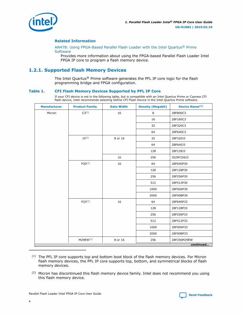
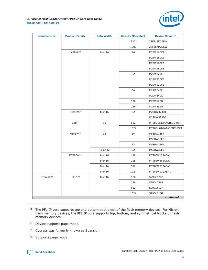
1.2.1. Supported Flash Memory Devices
The Intel Quartus® Prime software generates the PFL IP core logic for the flashprogramming bridge and FPGA configuration.
Table 1. CFI Flash Memory Devices Supported by PFL IP CoreIf your CFI device is not in the following table, but is compatible with an Intel Quartus Prime or Cypress CFIflash device, Intel recommends selecting Define CFI Flash Device in the Intel Quartus Prime software.
Manufacturer Product Family Data Width Density (Megabit) Device Name(1)
Micron C3(2) 16 8 28F800C3
16 28F160C3
32 28F320C3
64 28F640C3
J3(2) 8 or 16 32 28F320J3
64 28F640J3
128 28F128J3
16 256 JS29F256J3
P30(2) 16 64 28F640P30
128 28F128P30
256 28F256P30
512 28F512P30
1000 28F00AP30
2000 28F00BP30
P33(2) 16 64 28F640P33
128 28F128P33
256 28F256P33
512 28F512P33
1000 28F00AP33
2000 28F00BP33
M29EW(2) 8 or 16 256 28F256M29EW
continued...
(1) The PFL IP core supports top and bottom boot block of the flash memory devices. For Micronflash memory devices, the PFL IP core supports top, bottom, and symmetrical blocks of flashmemory devices.
(2) Micron has discontinued this flash memory device family. Intel does not recommend you usingthis flash memory device.
1. Parallel Flash Loader Intel® FPGA IP Core User Guide
UG-01082 | 2019.02.19
Parallel Flash Loader Intel FPGA IP Core User Guide Send Feedback
4
Manufacturer Product Family Data Width Density (Megabit) Device Name(1)
512 28F512M29EW
1000 28F00AM29EW
M29W(2) 8 or 16 16 M28W160CT
M28W160CB
M29W160F7
M29W160FB
32 M29W320E
M29W320FT
M29W320FB
64 M29W640F
M29W640G
128 M29W128G
256 M29W256G
M29DW(2) 8 or 16 32 M29DW323DT
M29DW323DB
G18(2) 16 512 MT28GU512AAA1EGC-0SIT
1024 MT28GU01GAAA1EGC-0SIT
M58BW(2) 32 16 M58BW16FT
M58BW16FB
32 M58BW32FT
16 or 32 32 M58BW32FB
MT28EW(3) 8 or 16 128 MT28EW128ABA1
8 or 16 256 MT28EW256ABA1
8 or 16 512 MT28EW512ABA1
8 or 16 1024 MT28EW01GABA1
Cypress(4) GL-P(5) 8 or 16 128 S29GL128P
256 S29GL256P
512 S29GL512P
1024 S29GL01GP
continued...
(1) The PFL IP core supports top and bottom boot block of the flash memory devices. For Micronflash memory devices, the PFL IP core supports top, bottom, and symmetrical blocks of flashmemory devices.
(3) Device supports page mode.
(4) Cypress was formerly known as Spansion.
(5) Supports page mode.
1. Parallel Flash Loader Intel® FPGA IP Core User Guide
UG-01082 | 2019.02.19
Send Feedback Parallel Flash Loader Intel FPGA IP Core User Guide
5
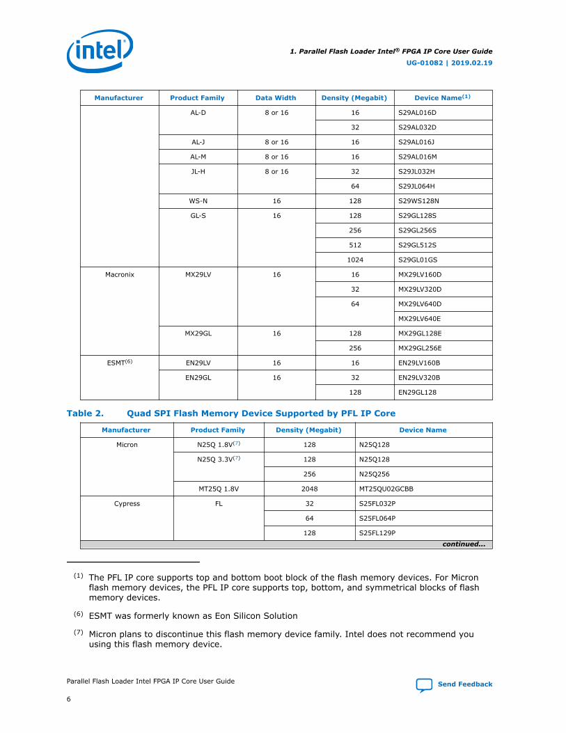
Manufacturer Product Family Data Width Density (Megabit) Device Name(1)
AL-D 8 or 16 16 S29AL016D
32 S29AL032D
AL-J 8 or 16 16 S29AL016J
AL-M 8 or 16 16 S29AL016M
JL-H 8 or 16 32 S29JL032H
64 S29JL064H
WS-N 16 128 S29WS128N
GL-S 16 128 S29GL128S
256 S29GL256S
512 S29GL512S
1024 S29GL01GS
Macronix MX29LV 16 16 MX29LV160D
32 MX29LV320D
64 MX29LV640D
MX29LV640E
MX29GL 16 128 MX29GL128E
256 MX29GL256E
ESMT(6) EN29LV 16 16 EN29LV160B
EN29GL 16 32 EN29LV320B
128 EN29GL128
Table 2. Quad SPI Flash Memory Device Supported by PFL IP Core
Manufacturer Product Family Density (Megabit) Device Name
Micron N25Q 1.8V(7) 128 N25Q128
N25Q 3.3V(7) 128 N25Q128
256 N25Q256
MT25Q 1.8V 2048 MT25QU02GCBB
Cypress FL 32 S25FL032P
64 S25FL064P
128 S25FL129P
continued...
(1) The PFL IP core supports top and bottom boot block of the flash memory devices. For Micronflash memory devices, the PFL IP core supports top, bottom, and symmetrical blocks of flashmemory devices.
(6) ESMT was formerly known as Eon Silicon Solution
(7) Micron plans to discontinue this flash memory device family. Intel does not recommend youusing this flash memory device.
1. Parallel Flash Loader Intel® FPGA IP Core User Guide
UG-01082 | 2019.02.19
Parallel Flash Loader Intel FPGA IP Core User Guide Send Feedback
6
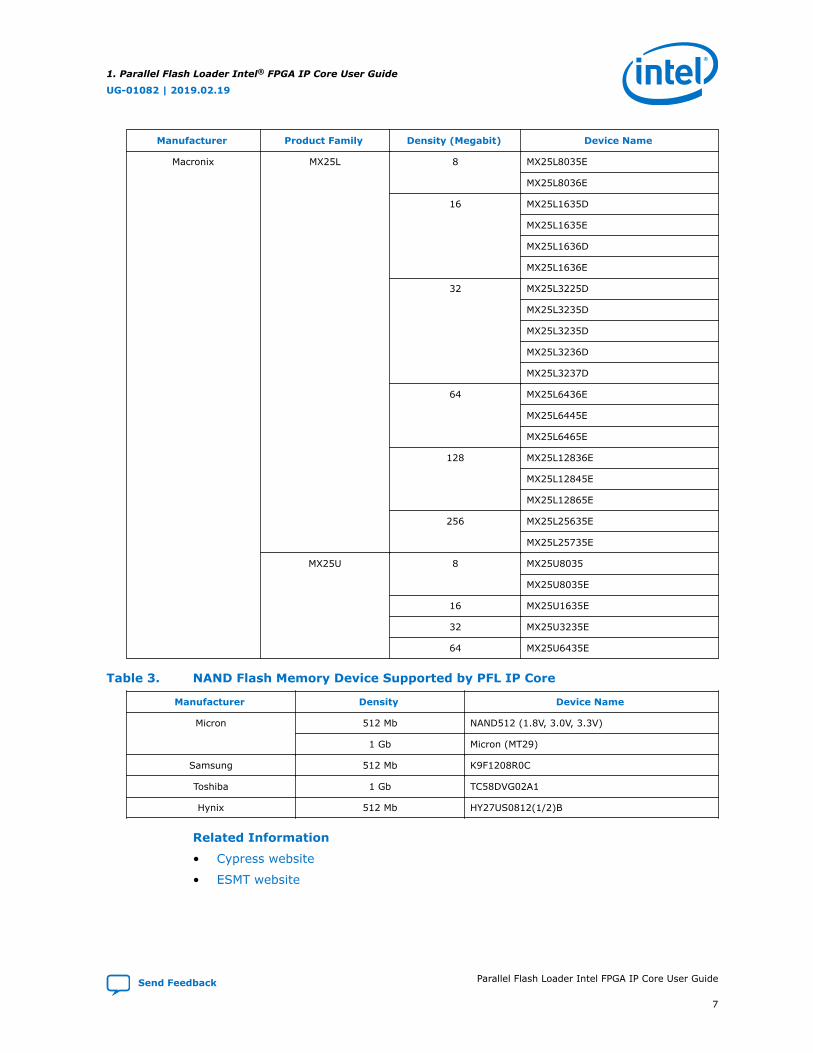
Manufacturer Product Family Density (Megabit) Device Name
Macronix MX25L 8 MX25L8035E
MX25L8036E
16 MX25L1635D
MX25L1635E
MX25L1636D
MX25L1636E
32 MX25L3225D
MX25L3235D
MX25L3235D
MX25L3236D
MX25L3237D
64 MX25L6436E
MX25L6445E
MX25L6465E
128 MX25L12836E
MX25L12845E
MX25L12865E
256 MX25L25635E
MX25L25735E
MX25U 8 MX25U8035
MX25U8035E
16 MX25U1635E
32 MX25U3235E
64 MX25U6435E
Table 3. NAND Flash Memory Device Supported by PFL IP Core
Manufacturer Density Device Name
Micron 512 Mb NAND512 (1.8V, 3.0V, 3.3V)
1 Gb Micron (MT29)
Samsung 512 Mb K9F1208R0C
Toshiba 1 Gb TC58DVG02A1
Hynix 512 Mb HY27US0812(1/2)B
Related Information
• Cypress website
• ESMT website
1. Parallel Flash Loader Intel® FPGA IP Core User Guide
UG-01082 | 2019.02.19
Send Feedback Parallel Flash Loader Intel FPGA IP Core User Guide
7
1.2.2. Supported Schemes and Features
The PFL IP core allows you to configure the FPGA in passive serial (PS) or fast passiveparallel (FPP) scheme. The PFL IP core supports configuration with FPGA on-chip datacompression and data encryption.
When you use compressed or encrypted configuration data for FPP configuration, thePFL IP core holds one data byte for one, two, four, or eight DCLK cycles to ensure theDCLK frequency runs at the required data rate as specified by the DCLK-to-DATA[]Ratio. The PFL IP core checks if the compression or encryption feature is turned on inthe configuration image before configuring in FPP mode. Hence, no additional settingis required in the PFL IP core to specify whether the configuration file stored in theflash memory device is a compressed or uncompressed image.
Note: When you turn on the enhanced bitstream compression feature, data encryption isdisabled.
You can program the Intel CPLDs and flash memory device in Programmer Object File(.pof), Jam™ Standard Test and Programming Language (STAPL) Format File (.jam),or JAM Byte Code File (.jbc) file format. The PFL IP core does not support Raw BinaryFile (.rbf) format.
Logic element (LE) usage varies with different PFL IP core and software settings. Todetermine the exact LE usage number, compile a PFL design with your settings usingthe software.
1.3. Functional Description
The PFL IP core allows you to program flash memory devices with Intel CPLDs throughthe JTAG interface and provides the logic to control configuration from the flashmemory device to the Intel FPGA.
1.3.1. Programming Flash Memory
You can use the PFL IP core to program the following flash memory devices with JTAGinterface:
• Programming CFI Flash
• Programming Quad SPI Flash
• Programming NAND Flash
Related Information
• Supported Flash Memory Devices on page 4
• Third-party Programmer Support on page 38Provides more information about programming the flash memory using third-party tools.
1.3.1.1. Programming CFI Flash
Intel configuration devices support programming through the JTAG interface to allowin-system programming and updates. However, standard flash memory devices do notsupport the JTAG interface. You can use the JTAG interface in Intel CPLDs to indirectlyprogram the flash memory device.
1. Parallel Flash Loader Intel® FPGA IP Core User Guide
UG-01082 | 2019.02.19
Parallel Flash Loader Intel FPGA IP Core User Guide Send Feedback
8
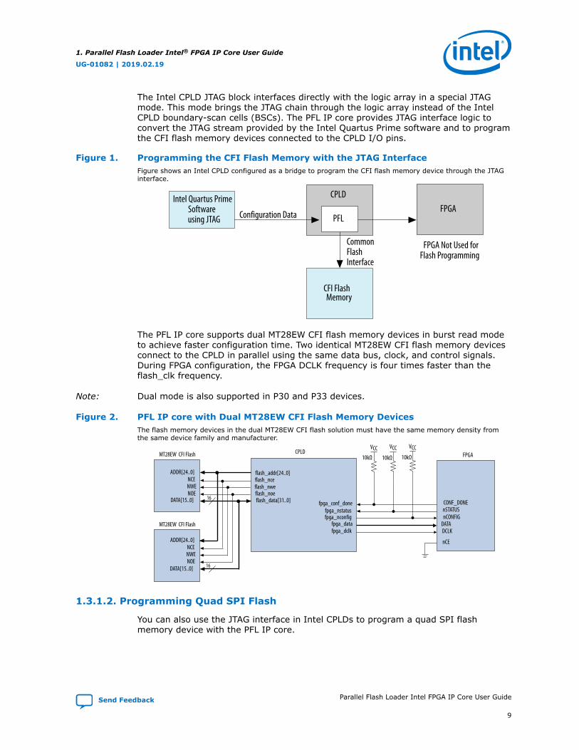
The Intel CPLD JTAG block interfaces directly with the logic array in a special JTAGmode. This mode brings the JTAG chain through the logic array instead of the IntelCPLD boundary-scan cells (BSCs). The PFL IP core provides JTAG interface logic toconvert the JTAG stream provided by the Intel Quartus Prime software and to programthe CFI flash memory devices connected to the CPLD I/O pins.
Figure 1. Programming the CFI Flash Memory with the JTAG InterfaceFigure shows an Intel CPLD configured as a bridge to program the CFI flash memory device through the JTAGinterface.
CPLD
CFI FlashMemory
FPGAConfiguration Data
CommonFlashInterface
PFL
Intel Quartus PrimeSoftwareusing JTAG
FPGA Not Used forFlash Programming
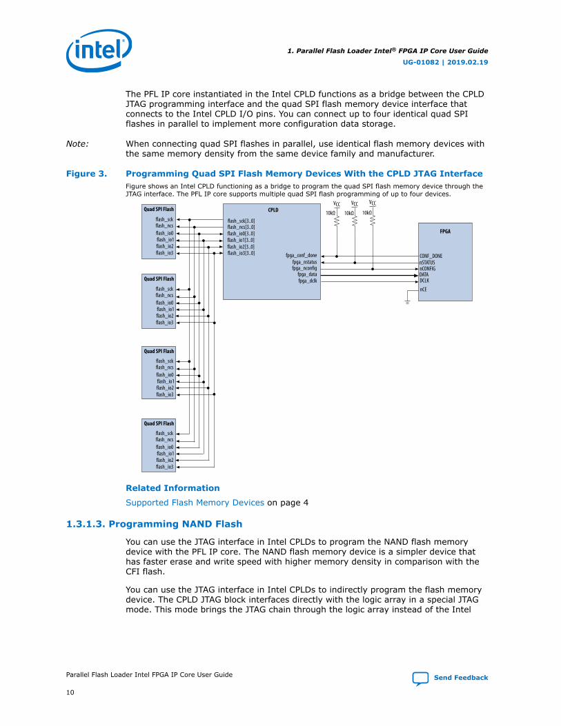
The PFL IP core supports dual MT28EW CFI flash memory devices in burst read modeto achieve faster configuration time. Two identical MT28EW CFI flash memory devicesconnect to the CPLD in parallel using the same data bus, clock, and control signals.During FPGA configuration, the FPGA DCLK frequency is four times faster than theflash_clk frequency.
Note: Dual mode is also supported in P30 and P33 devices.
Figure 2. PFL IP core with Dual MT28EW CFI Flash Memory DevicesThe flash memory devices in the dual MT28EW CFI flash solution must have the same memory density fromthe same device family and manufacturer.
VCC VCC VCC MT28EW CFI Flash CPLD FPGA
MT28EW CFI Flash
16
16
10kΩ 10kΩ 10kΩ
ADDR[24..0]NCENWENOE
DATA[15..0]
ADDR[24..0]NCENWENOE
DATA[15..0]
flash_addr[24..0]flash_nceflash_nweflash_noeflash_data[31..0] fpga_conf_done
fpga_nstatusfpga_nconfig
fpga_datafpga_dclk
CONF_DONEnSTATUSnCONFIG
DATA
nCE
DCLK
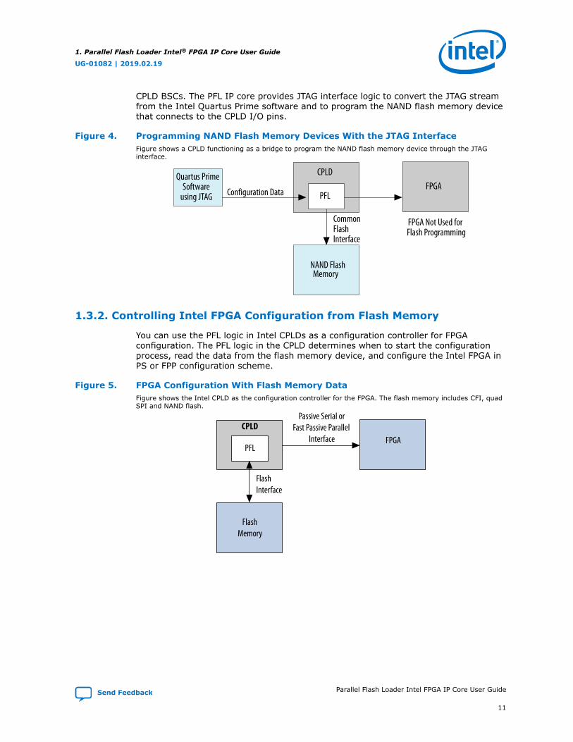
1.3.1.2. Programming Quad SPI Flash
You can also use the JTAG interface in Intel CPLDs to program a quad SPI flashmemory device with the PFL IP core.
1. Parallel Flash Loader Intel® FPGA IP Core User Guide
UG-01082 | 2019.02.19
Send Feedback Parallel Flash Loader Intel FPGA IP Core User Guide
9
The PFL IP core instantiated in the Intel CPLD functions as a bridge between the CPLDJTAG programming interface and the quad SPI flash memory device interface thatconnects to the Intel CPLD I/O pins. You can connect up to four identical quad SPIflashes in parallel to implement more configuration data storage.
Note: When connecting quad SPI flashes in parallel, use identical flash memory devices withthe same memory density from the same device family and manufacturer.
Figure 3. Programming Quad SPI Flash Memory Devices With the CPLD JTAG InterfaceFigure shows an Intel CPLD functioning as a bridge to program the quad SPI flash memory device through theJTAG interface. The PFL IP core supports multiple quad SPI flash programming of up to four devices.
VCC VCC VCCQuad SPI Flash CPLD
FPGA
10kΩ 10kΩ 10kΩflash_sck
flash_io0flash_io1flash_io2flash_io3
flash_sck[3..0]
flash_io0[3..0]flash_io1[3..0]flash_io2[3..0]flash_io3[3..0] fpga_conf_done
fpga_nstatusfpga_nconfig
fpga_datafpga_dclk
CONF_DONEnSTATUSnCONFIGDATA
nCE
DCLK
flash_ncs flash_ncs[3..0]
Quad SPI Flash
flash_sck
flash_io0flash_io1flash_io2flash_io3
flash_ncs
Quad SPI Flash
flash_sck
flash_io0flash_io1flash_io2flash_io3
flash_ncs
Quad SPI Flash
flash_sck
flash_io0flash_io1flash_io2flash_io3
flash_ncs
Related Information
Supported Flash Memory Devices on page 4
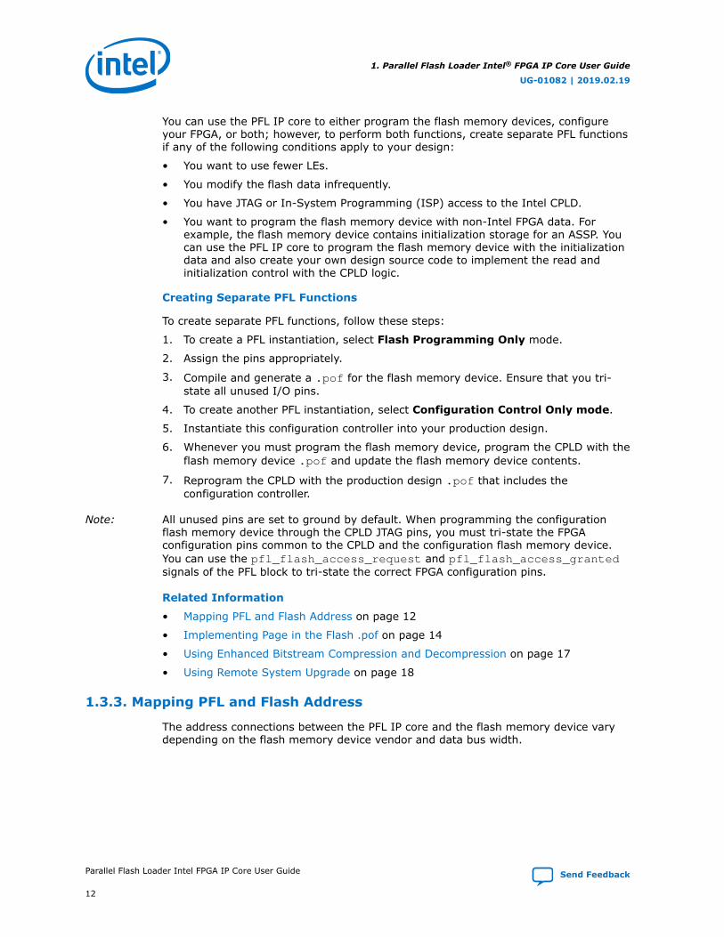
1.3.1.3. Programming NAND Flash
You can use the JTAG interface in Intel CPLDs to program the NAND flash memorydevice with the PFL IP core. The NAND flash memory device is a simpler device thathas faster erase and write speed with higher memory density in comparison with theCFI flash.
You can use the JTAG interface in Intel CPLDs to indirectly program the flash memorydevice. The CPLD JTAG block interfaces directly with the logic array in a special JTAGmode. This mode brings the JTAG chain through the logic array instead of the Intel
1. Parallel Flash Loader Intel® FPGA IP Core User Guide
UG-01082 | 2019.02.19
Parallel Flash Loader Intel FPGA IP Core User Guide Send Feedback
10
CPLD BSCs. The PFL IP core provides JTAG interface logic to convert the JTAG streamfrom the Intel Quartus Prime software and to program the NAND flash memory devicethat connects to the CPLD I/O pins.
Figure 4. Programming NAND Flash Memory Devices With the JTAG InterfaceFigure shows a CPLD functioning as a bridge to program the NAND flash memory device through the JTAGinterface.
CPLD
NAND FlashMemory
FPGAConfiguration Data
CommonFlashInterface
PFL
Quartus PrimeSoftware
using JTAG
FPGA Not Used forFlash Programming
1.3.2. Controlling Intel FPGA Configuration from Flash Memory
You can use the PFL logic in Intel CPLDs as a configuration controller for FPGAconfiguration. The PFL logic in the CPLD determines when to start the configurationprocess, read the data from the flash memory device, and configure the Intel FPGA inPS or FPP configuration scheme.
Figure 5. FPGA Configuration With Flash Memory DataFigure shows the Intel CPLD as the configuration controller for the FPGA. The flash memory includes CFI, quadSPI and NAND flash.
CPLD
FlashMemory
FPGA
FlashInterface
PFL
Passive Serial orFast Passive Parallel
Interface
1. Parallel Flash Loader Intel® FPGA IP Core User Guide
UG-01082 | 2019.02.19
Send Feedback Parallel Flash Loader Intel FPGA IP Core User Guide
11
You can use the PFL IP core to either program the flash memory devices, configureyour FPGA, or both; however, to perform both functions, create separate PFL functionsif any of the following conditions apply to your design:
• You want to use fewer LEs.
• You modify the flash data infrequently.
• You have JTAG or In-System Programming (ISP) access to the Intel CPLD.
• You want to program the flash memory device with non-Intel FPGA data. Forexample, the flash memory device contains initialization storage for an ASSP. Youcan use the PFL IP core to program the flash memory device with the initializationdata and also create your own design source code to implement the read andinitialization control with the CPLD logic.
Creating Separate PFL Functions
To create separate PFL functions, follow these steps:
1. To create a PFL instantiation, select Flash Programming Only mode.
2. Assign the pins appropriately.
3. Compile and generate a .pof for the flash memory device. Ensure that you tri-state all unused I/O pins.
4. To create another PFL instantiation, select Configuration Control Only mode.
5. Instantiate this configuration controller into your production design.
6. Whenever you must program the flash memory device, program the CPLD with theflash memory device .pof and update the flash memory device contents.
7. Reprogram the CPLD with the production design .pof that includes theconfiguration controller.
Note: All unused pins are set to ground by default. When programming the configurationflash memory device through the CPLD JTAG pins, you must tri-state the FPGAconfiguration pins common to the CPLD and the configuration flash memory device.You can use the pfl_flash_access_request and pfl_flash_access_grantedsignals of the PFL block to tri-state the correct FPGA configuration pins.
Related Information
• Mapping PFL and Flash Address on page 12
• Implementing Page in the Flash .pof on page 14
• Using Enhanced Bitstream Compression and Decompression on page 17
• Using Remote System Upgrade on page 18
1.3.3. Mapping PFL and Flash Address
The address connections between the PFL IP core and the flash memory device varydepending on the flash memory device vendor and data bus width.
1. Parallel Flash Loader Intel® FPGA IP Core User Guide
UG-01082 | 2019.02.19
Parallel Flash Loader Intel FPGA IP Core User Guide Send Feedback
12
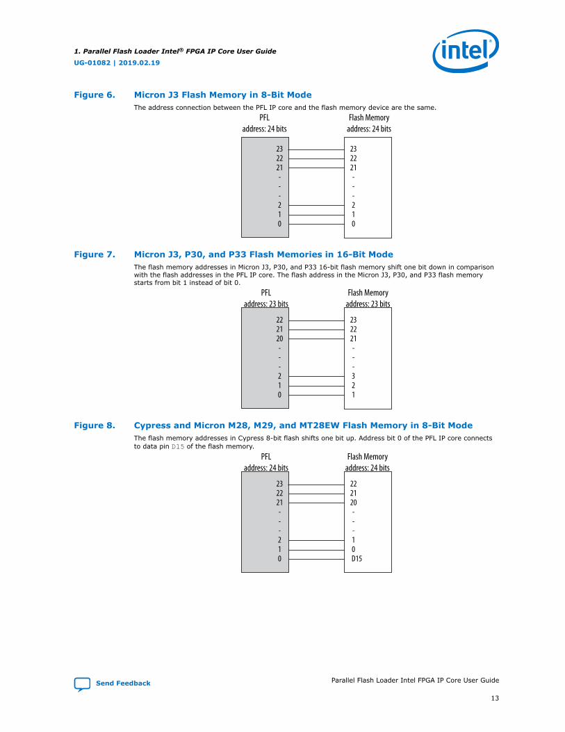
Figure 6. Micron J3 Flash Memory in 8-Bit ModeThe address connection between the PFL IP core and the flash memory device are the same.
232221---210
PFLaddress: 24 bits
232221---210
Flash Memoryaddress: 24 bits
Figure 7. Micron J3, P30, and P33 Flash Memories in 16-Bit ModeThe flash memory addresses in Micron J3, P30, and P33 16-bit flash memory shift one bit down in comparisonwith the flash addresses in the PFL IP core. The flash address in the Micron J3, P30, and P33 flash memorystarts from bit 1 instead of bit 0.
222120---210
PFLaddress: 23 bits
232221---321
Flash Memoryaddress: 23 bits
Figure 8. Cypress and Micron M28, M29, and MT28EW Flash Memory in 8-Bit ModeThe flash memory addresses in Cypress 8-bit flash shifts one bit up. Address bit 0 of the PFL IP core connectsto data pin D15 of the flash memory.
232221---210
PFLaddress: 24 bits
222120---10
D15
Flash Memoryaddress: 24 bits
1. Parallel Flash Loader Intel® FPGA IP Core User Guide
UG-01082 | 2019.02.19
Send Feedback Parallel Flash Loader Intel FPGA IP Core User Guide
13
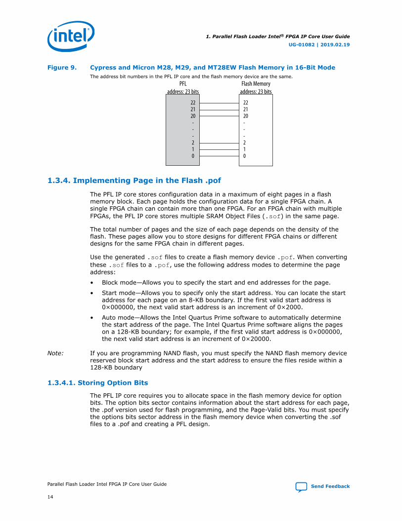
Figure 9. Cypress and Micron M28, M29, and MT28EW Flash Memory in 16-Bit ModeThe address bit numbers in the PFL IP core and the flash memory device are the same.
222120---210
PFLaddress: 23 bits
222120---210
Flash Memoryaddress: 23 bits
1.3.4. Implementing Page in the Flash .pof
The PFL IP core stores configuration data in a maximum of eight pages in a flashmemory block. Each page holds the configuration data for a single FPGA chain. Asingle FPGA chain can contain more than one FPGA. For an FPGA chain with multipleFPGAs, the PFL IP core stores multiple SRAM Object Files (.sof) in the same page.
The total number of pages and the size of each page depends on the density of theflash. These pages allow you to store designs for different FPGA chains or differentdesigns for the same FPGA chain in different pages.
Use the generated .sof files to create a flash memory device .pof. When convertingthese .sof files to a .pof, use the following address modes to determine the pageaddress:
• Block mode—Allows you to specify the start and end addresses for the page.
• Start mode—Allows you to specify only the start address. You can locate the startaddress for each page on an 8-KB boundary. If the first valid start address is0×000000, the next valid start address is an increment of 0×2000.
• Auto mode—Allows the Intel Quartus Prime software to automatically determinethe start address of the page. The Intel Quartus Prime software aligns the pageson a 128-KB boundary; for example, if the first valid start address is 0×000000,the next valid start address is an increment of 0×20000.
Note: If you are programming NAND flash, you must specify the NAND flash memory devicereserved block start address and the start address to ensure the files reside within a128-KB boundary
1.3.4.1. Storing Option Bits
The PFL IP core requires you to allocate space in the flash memory device for optionbits. The option bits sector contains information about the start address for each page,the .pof version used for flash programming, and the Page-Valid bits. You must specifythe options bits sector address in the flash memory device when converting the .soffiles to a .pof and creating a PFL design.
1. Parallel Flash Loader Intel® FPGA IP Core User Guide
UG-01082 | 2019.02.19
Parallel Flash Loader Intel FPGA IP Core User Guide Send Feedback
14
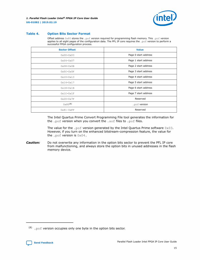
Table 4. Option Bits Sector FormatOffset address 0x80 stores the .pof version required for programming flash memory. This .pof versionapplies to all eight pages of the configuration data. The PFL IP core requires the .pof version to perform asuccessful FPGA configuration process.
Sector Offset Value
0x00–0x03 Page 0 start address
0x04–0x07 Page 1 start address
0x08–0x0B Page 2 start address
0x0C–0x0F Page 3 start address
0x10–0x13 Page 4 start address
0x14–0x17 Page 5 start address
0x18–0x1B Page 6 start address
0x1C–0x1F Page 7 start address
0x20–0x7F Reserved
0x80(8) .pof version
0x81–0xFF Reserved
The Intel Quartus Prime Convert Programming File tool generates the information forthe .pof version when you convert the .sof files to .pof files.
The value for the .pof version generated by the Intel Quartus Prime software 0x03.However, if you turn on the enhanced bitstream-compression feature, the value forthe .pof version is 0x04.
Caution: Do not overwrite any information in the option bits sector to prevent the PFL IP corefrom malfunctioning, and always store the option bits in unused addresses in the flashmemory device.
(8) .pof version occupies only one byte in the option bits sector.
1. Parallel Flash Loader Intel® FPGA IP Core User Guide
UG-01082 | 2019.02.19
Send Feedback Parallel Flash Loader Intel FPGA IP Core User Guide
15
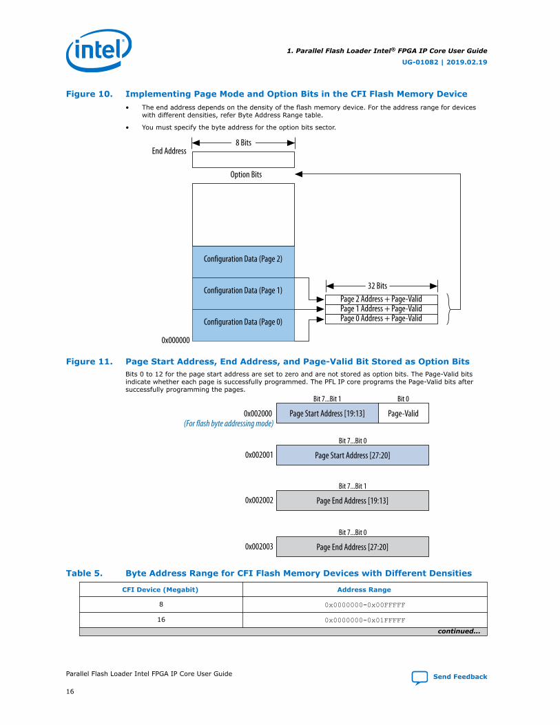
Figure 10. Implementing Page Mode and Option Bits in the CFI Flash Memory Device• The end address depends on the density of the flash memory device. For the address range for devices
with different densities, refer Byte Address Range table.
• You must specify the byte address for the option bits sector.
Option Bits
Configuration Data (Page 2)
Configuration Data (Page 1)
Configuration Data (Page 0)
Page 2 Address + Page-ValidPage 1 Address + Page-ValidPage 0 Address + Page-Valid
End Address
0x000000
8 Bits
32 Bits
Figure 11. Page Start Address, End Address, and Page-Valid Bit Stored as Option BitsBits 0 to 12 for the page start address are set to zero and are not stored as option bits. The Page-Valid bitsindicate whether each page is successfully programmed. The PFL IP core programs the Page-Valid bits aftersuccessfully programming the pages.
Page Start Address [19:13] Page-Valid
Bit 7...Bit 1 Bit 0
Page Start Address [27:20]
Bit 7...Bit 0
0x002000
0x002001
Page End Address [19:13]
Bit 7...Bit 1
0x002002
Page End Address [27:20]
Bit 7...Bit 0
0x002003
(For flash byte addressing mode)
Table 5. Byte Address Range for CFI Flash Memory Devices with Different Densities
CFI Device (Megabit) Address Range
8 0x0000000–0x00FFFFF
16 0x0000000–0x01FFFFF
continued...
1. Parallel Flash Loader Intel® FPGA IP Core User Guide
UG-01082 | 2019.02.19
Parallel Flash Loader Intel FPGA IP Core User Guide Send Feedback
16
CFI Device (Megabit) Address Range
32 0x0000000–0x03FFFFF
64 0x0000000–0x07FFFFF
128 0x0000000–0x0FFFFFF
256 0x0000000–0x1FFFFFF
512 0x0000000–0x3FFFFFF
1024 0x0000000–0x7FFFFFF
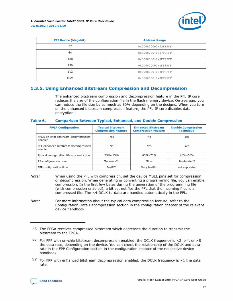
1.3.5. Using Enhanced Bitstream Compression and Decompression
The enhanced bitstream compression and decompression feature in the PFL IP corereduces the size of the configuration file in the flash memory device. On average, youcan reduce the file size by as much as 50% depending on the designs. When you turnon the enhanced bitstream compression feature, the PFL IP core disables dataencryption.
Table 6. Comparison Between Typical, Enhanced, and Double Compression
FPGA Configuration Typical BitstreamCompression Feature
Enhanced BitstreamCompression Feature
Double CompressionTechnique
FPGA on-chip bitstream decompressionenabled
Yes No Yes
PFL enhanced bitstream decompressionenabled
No Yes Yes
Typical configuration file size reduction 35%–55% 45%–75% 40%–60%
PS configuration time Moderate(9) Slow Moderate(9)
FPP configuration time Fast(10) Very fast(11) Not supported
Note: When using the PFL with compression, set the device MSEL pins set for compressionor decompression. When generating or converting a programming file, you can enablecompression. In the first few bytes during the generation of the programming file(with compression enabled), a bit set notifies the PFL that the incoming files is acompressed file. The ×4 DCLK-to-data are handled automatically in the PFL.
Note: For more information about the typical data compression feature, refer to theConfiguration Data Decompression section in the configuration chapter of the relevantdevice handbook.
(9) The FPGA receives compressed bitstream which decreases the duration to transmit thebitstream to the FPGA.
(10) For FPP with on-chip bitstream decompression enabled, the DCLK frequency is ×2, ×4, or ×8the data rate, depending on the device. You can check the relationship of the DCLK and datarate in the FPP Configuration section in the configuration chapter of the respective devicehandbook.
(11) For FPP with enhanced bitstream decompression enabled, the DCLK frequency is ×1 the datarate.
1. Parallel Flash Loader Intel® FPGA IP Core User Guide
UG-01082 | 2019.02.19
Send Feedback Parallel Flash Loader Intel FPGA IP Core User Guide
17

For the FPP configuration scheme, the enhanced bitstream compression feature helpsachieve higher configuration data compression ratio and faster configuration time. Forthe PS configuration scheme, the double compression technique helps achieve higherconfiguration data compression ratio and moderate configuration time. To enable thedouble compression technique, turn on both the typical bitstream compression featureand the enhanced bitstream compression feature in the PFL parameter editor.
Figure 12. FPGA Configuration Data Flow with Enhanced Bitstream Compression Featurein PS or FPP Configuration Scheme
CPLD
CFI or Quad SPI Flash Memory
FPGAPFL withEnhancedBitstream
DecompressionFeature
Compressed Data
Passive Serial or Fast Passive Parallel With
Uncompressed Data
Figure 13. FPGA Configuration Data Flow with Double Compression Technique in PSConfiguration Scheme
CPLD
CFI or Quad SPIFlash Memory
PFL withEnhancedBitstream
DecompressionFeature
Double Compressed Data
Passive Serial WithCompressed Data
FPGA
On-ChipBitstream
DecompressionFeature
1.3.6. Using Remote System Upgrade
When you instantiate the PFL IP core in the Intel CPLD for FPP or PS configuration, youcan use the features in the PFL IP core to perform remote system upgrade.
1. Parallel Flash Loader Intel® FPGA IP Core User Guide
UG-01082 | 2019.02.19
Parallel Flash Loader Intel FPGA IP Core User Guide Send Feedback
18
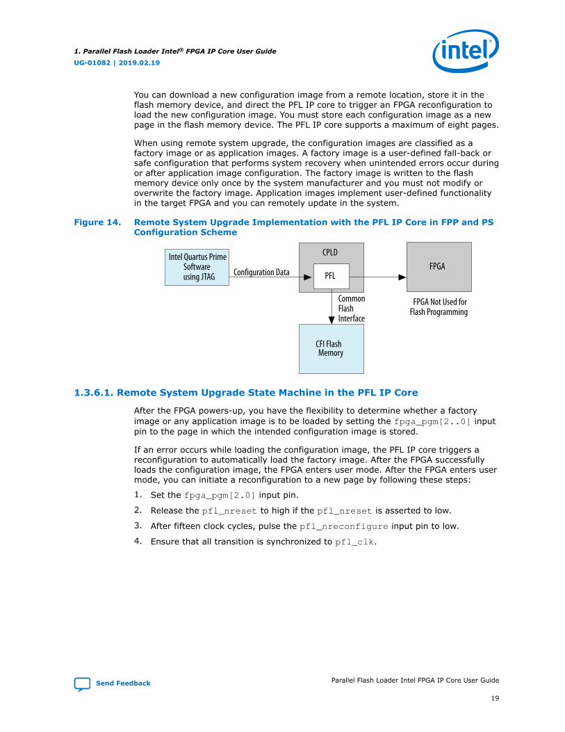
You can download a new configuration image from a remote location, store it in theflash memory device, and direct the PFL IP core to trigger an FPGA reconfiguration toload the new configuration image. You must store each configuration image as a newpage in the flash memory device. The PFL IP core supports a maximum of eight pages.
When using remote system upgrade, the configuration images are classified as afactory image or as application images. A factory image is a user-defined fall-back orsafe configuration that performs system recovery when unintended errors occur duringor after application image configuration. The factory image is written to the flashmemory device only once by the system manufacturer and you must not modify oroverwrite the factory image. Application images implement user-defined functionalityin the target FPGA and you can remotely update in the system.
Figure 14. Remote System Upgrade Implementation with the PFL IP Core in FPP and PSConfiguration Scheme
CPLD
CFI FlashMemory
FPGAConfiguration Data
CommonFlashInterface
PFL
Intel Quartus PrimeSoftwareusing JTAG
FPGA Not Used forFlash Programming
1.3.6.1. Remote System Upgrade State Machine in the PFL IP Core
After the FPGA powers-up, you have the flexibility to determine whether a factoryimage or any application image is to be loaded by setting the fpga_pgm[2..0] inputpin to the page in which the intended configuration image is stored.
If an error occurs while loading the configuration image, the PFL IP core triggers areconfiguration to automatically load the factory image. After the FPGA successfullyloads the configuration image, the FPGA enters user mode. After the FPGA enters usermode, you can initiate a reconfiguration to a new page by following these steps:
1. Set the fpga_pgm[2.0] input pin.
2. Release the pfl_nreset to high if the pfl_nreset is asserted to low.
3. After fifteen clock cycles, pulse the pfl_nreconfigure input pin to low.
4. Ensure that all transition is synchronized to pfl_clk.
1. Parallel Flash Loader Intel® FPGA IP Core User Guide
UG-01082 | 2019.02.19
Send Feedback Parallel Flash Loader Intel FPGA IP Core User Guide
19
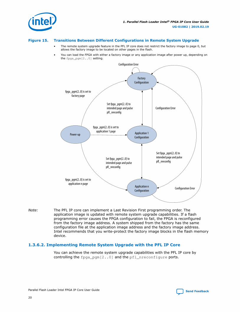
Figure 15. Transitions Between Different Configurations in Remote System Upgrade• The remote system upgrade feature in the PFL IP core does not restrict the factory image to page 0, but
allows the factory image to be located on other pages in the flash.
• You can load the FPGA with either a factory image or any application image after power up, depending onthe fpga_pgm[2..0] setting.
Application 1Configuration
Power-up
FactoryConfiguration
Application nConfiguration
fpga_pgm[2..0] is set tofactory page
Set fpga_pgm[2..0] to intended page and pulsepfl_nreconfig
fpga_pgm[2..0] is set toapplication 1 page
Configuration Error
Configuration Error
Configuration Error
fpga_pgm[2..0] is set toapplication n page
Set fpga_pgm[2..0] to intended page and pulsepfl_nreconfig
Set fpga_pgm[2..0] to intended page and pulsepfl_nreconfig
Note: The PFL IP core can implement a Last Revision First programming order. Theapplication image is updated with remote system upgrade capabilities. If a flashprogramming error causes the FPGA configuration to fail, the FPGA is reconfiguredfrom the factory image address. A system shipped from the factory has the sameconfiguration file at the application image address and the factory image address.Intel recommends that you write-protect the factory image blocks in the flash memorydevice.
1.3.6.2. Implementing Remote System Upgrade with the PFL IP Core
You can achieve the remote system upgrade capabilities with the PFL IP core bycontrolling the fpga_pgm[2..0] and the pfl_nreconfigure ports.
1. Parallel Flash Loader Intel® FPGA IP Core User Guide
UG-01082 | 2019.02.19
Parallel Flash Loader Intel FPGA IP Core User Guide Send Feedback
20
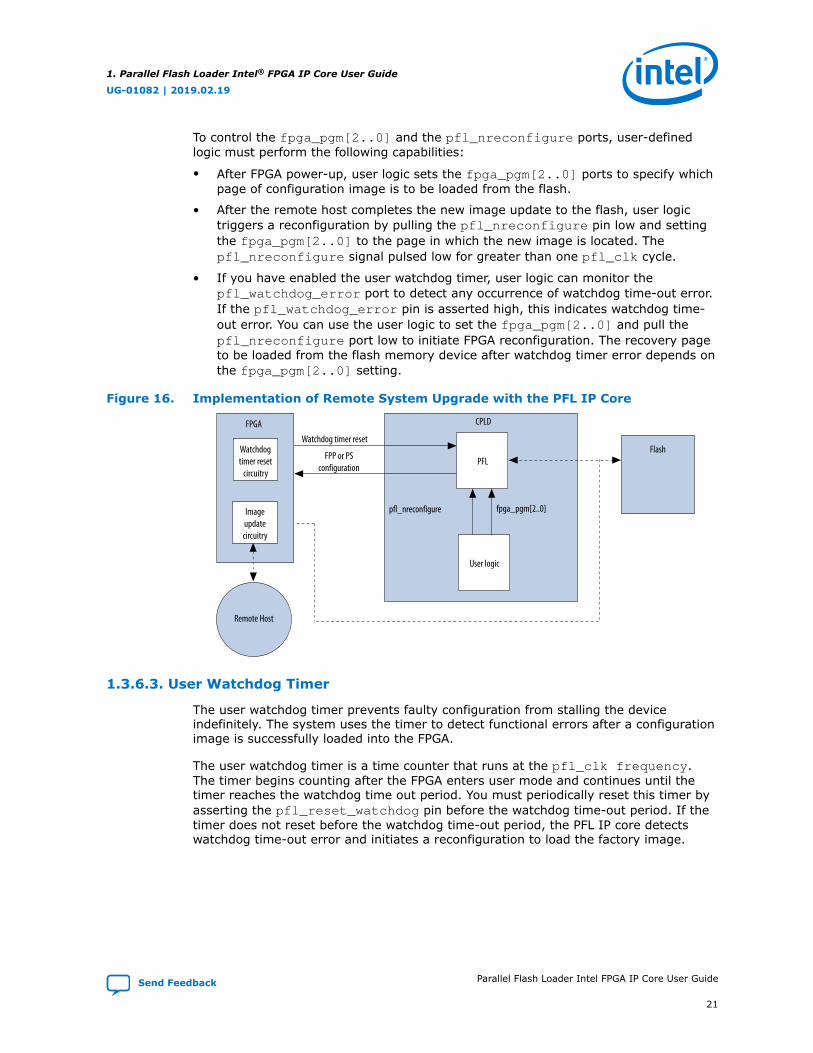
To control the fpga_pgm[2..0] and the pfl_nreconfigure ports, user-definedlogic must perform the following capabilities:
• After FPGA power-up, user logic sets the fpga_pgm[2..0] ports to specify whichpage of configuration image is to be loaded from the flash.
• After the remote host completes the new image update to the flash, user logictriggers a reconfiguration by pulling the pfl_nreconfigure pin low and settingthe fpga_pgm[2..0] to the page in which the new image is located. Thepfl_nreconfigure signal pulsed low for greater than one pfl_clk cycle.
• If you have enabled the user watchdog timer, user logic can monitor thepfl_watchdog_error port to detect any occurrence of watchdog time-out error.If the pfl_watchdog_error pin is asserted high, this indicates watchdog time-out error. You can use the user logic to set the fpga_pgm[2..0] and pull thepfl_nreconfigure port low to initiate FPGA reconfiguration. The recovery pageto be loaded from the flash memory device after watchdog timer error depends onthe fpga_pgm[2..0] setting.
Figure 16. Implementation of Remote System Upgrade with the PFL IP Core
FlashWatchdogtimer reset
circuitry
FPGA
Imageupdatecircuitry
Remote Host
PFL
Watchdog timer reset
User logic
FPP or PSconfiguration
pfl_nreconfigure fpga_pgm[2..0]
CPLD
1.3.6.3. User Watchdog Timer
The user watchdog timer prevents faulty configuration from stalling the deviceindefinitely. The system uses the timer to detect functional errors after a configurationimage is successfully loaded into the FPGA.
The user watchdog timer is a time counter that runs at the pfl_clk frequency.The timer begins counting after the FPGA enters user mode and continues until thetimer reaches the watchdog time out period. You must periodically reset this timer byasserting the pfl_reset_watchdog pin before the watchdog time-out period. If thetimer does not reset before the watchdog time-out period, the PFL IP core detectswatchdog time-out error and initiates a reconfiguration to load the factory image.
1. Parallel Flash Loader Intel® FPGA IP Core User Guide
UG-01082 | 2019.02.19
Send Feedback Parallel Flash Loader Intel FPGA IP Core User Guide
21
Instantiate the watchdog timer reset circuitry in the configuration image loaded intothe FPGA. Connect one output signal from the reset circuitry to thepfl_reset_watchdog pin of the PFL in the CPLD to periodically send a reset signalto the user watchdog timer. To reset the watchdog timer correctly, hold thepfl_reset_watchdog pin high or low for at least two pfl_clk cycles.
1.4. Using the PFL IP Core
This section describes the procedures on how to use the PFL IP core.
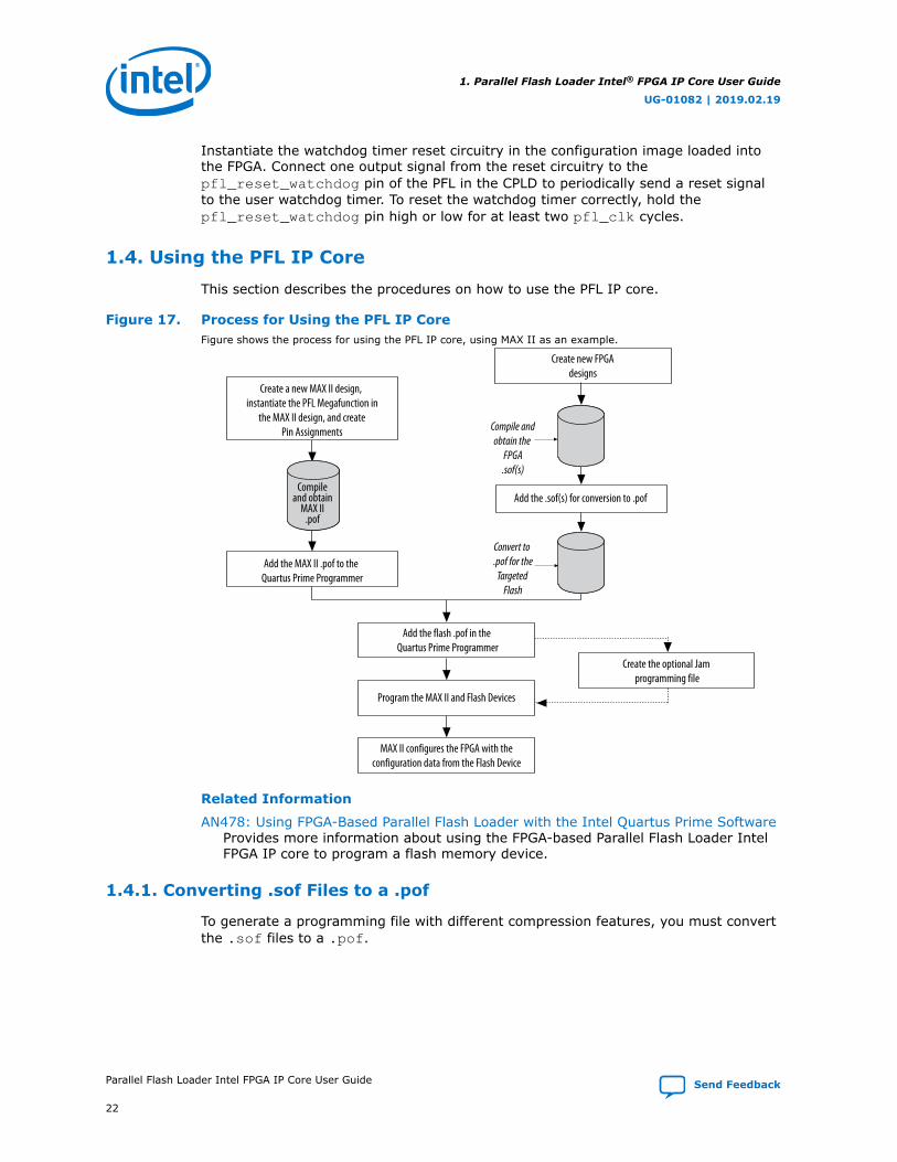
Figure 17. Process for Using the PFL IP CoreFigure shows the process for using the PFL IP core, using MAX II as an example.
Create a new MAX II design, instantiate the PFL Megafunction in
the MAX II design, and createPin Assignments
Add the MAX II .pof to the Quartus Prime Programmer
Add the flash .pof in the Quartus Prime Programmer
Program the MAX II and Flash Devices
MAX II configures the FPGA with theconfiguration data from the Flash Device
Compile andobtain the
FPGA .sof(s)
Convert to .pof for the
TargetedFlash
Compileand obtain
MAX II.pof
Add the .sof(s) for conversion to .pof
Create new FPGAdesigns
Create the optional Jam programming file
Related Information
AN478: Using FPGA-Based Parallel Flash Loader with the Intel Quartus Prime SoftwareProvides more information about using the FPGA-based Parallel Flash Loader IntelFPGA IP core to program a flash memory device.
1.4.1. Converting .sof Files to a .pof
To generate a programming file with different compression features, you must convertthe .sof files to a .pof.
1. Parallel Flash Loader Intel® FPGA IP Core User Guide
UG-01082 | 2019.02.19
Parallel Flash Loader Intel FPGA IP Core User Guide Send Feedback
22
To convert the .sof files to a .pof, follow these steps:
1. On the File menu, click Convert Programming Files.
2. For Programming file type, specify Programmer Object File (.pof) and namethe file.
3. For Configuration device, select the CFI or NAND flash memory device with thecorrect density. For example, CFI_32Mb is a CFI device with 32-Megabit (Mb)capacity.
4. To add the configuration data, under Input files to convert, select SOF Data.
5. Click Add File and browse to the .sof files you want to add.
You can place more than one .sof in the same page if you intend to configure achain of FPGAs. The order of the .sof files must follow the order of the devices inthe chain.
If you want to store the data from other .sof files in a different page, click AddSOF page. Add the .sof files to the new page.
6. Select SOF Data and click Properties to set the page number and name. UnderAddress mode for selected pages, select Auto to let the Intel Quartus Primesoftware automatically set the start address for that page. Select Block to specifythe start and end addresses, or select Start to specify the start address only.
7. Click OK.
8. You can also store Hexadecimal (Intel-Format) File (.hex) user data in the flashmemory device:
a. In the Input files to convert sub-window of the Convert ProgrammingFiles window, select Add Hex Data.
b. In the Add Hex Data dialog box, select either absolute or relative addressingmode.
— If you select absolute addressing mode, the data in the .hex is programmedin the flash memory device at the exact same address location listed inthe .hex.
— If you select relative addressing mode, specify a start address.
The data in the .hex is programmed into the flash memory device with the specificstart address, and the differences between the addresses are kept. If no addressis specified, the Intel Quartus Prime software selects an address.
Note: You can also add other non-configuration data to the .pof by selectingthe .hex that contains your data when creating the flash memorydevice .pof.
9. Click Options to specify the start address to store the option bits. This startaddress must be identical to the address you specify when creating the PFL IPcore. Ensure that the option bits sector does not overlap with the configurationdata pages and that the start address resides on an 8-KB boundary.
10. If you are using a NAND flash memory device, specify the reserved block startaddress and the start address (including the option bits) within a 128-KBboundary. To specify the address, in the File/Data area column, select NANDflash Reserved Block and click Properties.
11. To generate programming files with either the typical or enhanced bitstreamcompression feature, or both, perform one of the following steps:
1. Parallel Flash Loader Intel® FPGA IP Core User Guide
UG-01082 | 2019.02.19
Send Feedback Parallel Flash Loader Intel FPGA IP Core User Guide
23
— Typical bitstream compression feature
a. Select .sof under SOF Data.
b. Click Properties, and then turn on the Compression option.
c. Click OK.
— Enhanced bitstream compression feature
a. In the Options dialog box, turn on the Enable enhanced bitstream-compression when available option.
b. Click OK.
— Double compression technique
— Perform all the steps for the typical bitstream compression and enhancedbitstream compression features listed above.
Note: For more information about the compression feature in the PFL IP core,refer to “Using Enhanced Bitstream Compression and Decompression”.
12. To generate programming files with encrypted data, select .sof under SOF Dataand click Properties. Turn on the Generate encrypted bitstream check box.
13. Click OK to create the .pof.
Related Information
• Using Enhanced Bitstream Compression and Decompression on page 17
• Knowledge Center
1.4.2. Constraining PFL Timing
The PFL IP core supports the Intel Quartus Prime Timing Analyzer for accurate timinganalysis on the Intel IP cores. To perform timing analysis, you must define the clockcharacteristics, external path delays, and timing exceptions for the PFL input andoutput ports. This section provides guidelines for defining this information for PFLinput and output ports for use by the Timing Analyzer.
Note: The Timing Analyzer is a timing analysis tool that validates the timing performance ofthe logic in the design using industry-standard constraint, analysis, and reportingmethodology. For more information about the Timing Analyzer, refer to the IntelQuartus Prime Timing Analyzer chapter in volume 3 of the Intel Quartus PrimeHandbook.
Note: After you specify the timing constraint settings for the clock signal and for theasynchronous and synchronous input and output ports in the Timing Analyzer, on theConstraints menu, click Write SDC File to write all the constraints to a specificSystem Design Constraints File (.sdc). After the .sdc is written, run full compilationfor the PFL design.
Related Information
Intel Quartus Prime TimeQuest Timing Analyzer of the Intel Quartus Prime HandbookProvides more information about the TimeQuest analyzer.
1. Parallel Flash Loader Intel® FPGA IP Core User Guide
UG-01082 | 2019.02.19
Parallel Flash Loader Intel FPGA IP Core User Guide Send Feedback
24

1.4.2.1. Constraining Clock Signal
At any given time, one of the following two clock sources clocks the blocks andmodules of the PFL IP core:
• Clock signals from the pfl_clk ports of the PFL during FPGA configuration
• TCK pins of the JTAG programming interface during flash programming
The clock signal on the TCK pins is internally constrained to the maximum frequencysupported by the selected JTAG programming hardware. Constraining the clock signalis not mandatory.
You can constrain pfl_clk to the maximum frequency that the PFL IP core supports.You can use the create_clock command or the Create Clock dialog box to specifythe period and duty cycle of the clock constraint.
To constrain the pfl_clk signal in the Timing Analyzer, follow these steps:
1. Run full compilation for the PFL design. Ensure that the timing analysis tool is setto Timing Analyzer.
2. After full compilation completes, on the Tools menu, select Timing Analyzer tolaunch the Timing Analyzer window.
3. In the Tasks list, under Diagnostic, click Report Unconstrained Paths to viewthe list of unconstrained parts and ports of the PFL design.
4. In the Report list, under Unconstrained Paths, click Clock Summary to viewthe clock that requires constraints. The default setting for all unconstrained clocksis 1 GHz. To constrain the clock signal, right-click the clock name and select EditClock Constraint.
5. In the Create Clock dialog box, set the period and the duty cycle of the clockconstraint.
6. Click Run.
1.4.2.2. Constraining Synchronous Input and Output Ports
The setup and hold time of synchronous input and output ports is critical to thesystem designer. To avoid setup and hold time violations, you can specify the signaldelay from the FPGA or the flash memory device to the synchronous input and outputports of the PFL IP core. The Intel Quartus Prime Fitter places and routes the inputand output registers of the PFL IP core to meet the specified timing constraints.
Note: For more information about the synchronous input and output ports of the PFL IP core,refer to PFL Timing Constraints table.
The signal delay from FPGA or flash memory device to the PFL synchronous input portis specified by set_input_delay. The delay calculation is:
Input delay value = Board delay from FPGA or flash output port to the PFL input port+ TCO of the FPGA or flash memory device
The signal delay from PFL synchronous output port to FPGA or flash memory device isspecified by set_output_delay. The delay calculation is:
Output delay value = Board delay from the PFL output port to the FPGA or flash inputport + TSU of FPGA or flash device.
1. Parallel Flash Loader Intel® FPGA IP Core User Guide
UG-01082 | 2019.02.19
Send Feedback Parallel Flash Loader Intel FPGA IP Core User Guide
25

Note: TCO is the clock-to-output time from the timing specification in the FPGA, CPLD or flashdatasheet.
To constrain the synchronous input and output signals in the Timing Analyzer, followthese steps:
1. Run full compilation for the PFL design. Ensure that the timing analysis tool is setto Timing Analyzer.
2. After full compilation completes, on the Tools menu, select Timing Analyzer tolaunch the Timing Analyzer window.
3. In the Tasks list, under Diagnostic, click Report Unconstrained Paths to viewthe list of unconstrained parts and ports of the PFL design.
4. In the Report list, under the Unconstrained Paths category, select SetupAnalysis, and then click Unconstrained Input Port Paths.
5. Right-click each synchronous input or output port in the From list or To list andselect set_input_delay for the input port or set_output_delay for the outputport, then specify the input delay or output delay value.
Related Information
Summary of PFL Timing Constraints on page 26
1.4.2.3. Constraining Asynchronous Input and Output Ports
You can exclude asynchronous input and output ports from the timing analysis of thePFL IP core because the signals on these ports are not synchronous to a IP core clocksource. The internal structure of the PFL IP core handles the metastability of theseasynchronous signals.
To exclude asynchronous input and output ports from the timing analysis, use theset_false_path command to ignore these ports during timing analysis.
Note: After you specify all timing constraint settings for the clock signal, on the Constraintsmenu, click Write SDC File to write all the constraints to a specific .sdc. Then, runfull compilation for the PFL design again.
1.4.2.4. Summary of PFL Timing Constraints
Table 7. PFL Timing Constraints
Type Port Constraint Type Delay Value
Input clock pfl_clk create_clock Can be constrained up to themaximum frequency supported bythe PFL IP core.
Inputasynchronou
s
pfl_nreset set_false_path —
fpga_pgm set_false_path —
fpga_conf_done set_false_path —
fpga_nstatus set_false_path —
pfl_flash_access_granted set_false_path —
pfl_nreconfigure set_false_path —
continued...
1. Parallel Flash Loader Intel® FPGA IP Core User Guide
UG-01082 | 2019.02.19
Parallel Flash Loader Intel FPGA IP Core User Guide Send Feedback
26
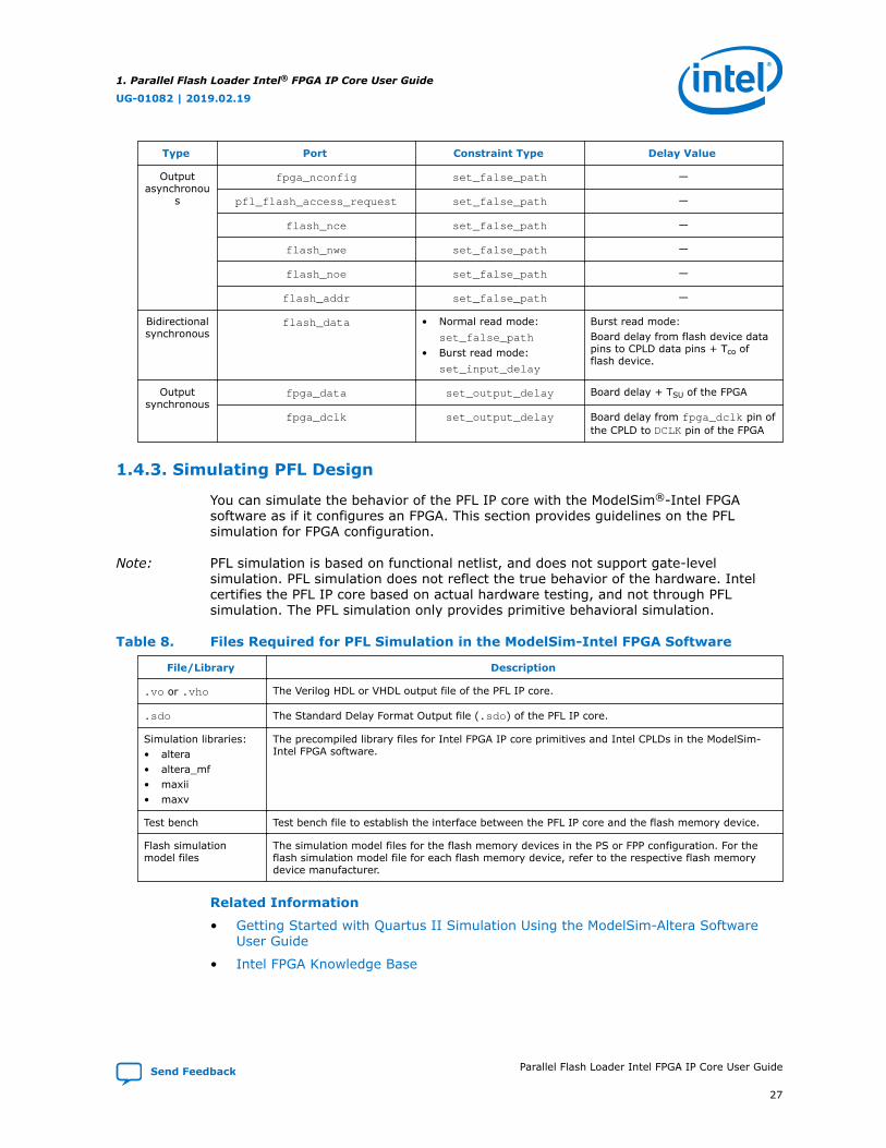
Type Port Constraint Type Delay Value
Outputasynchronou
s
fpga_nconfig set_false_path —
pfl_flash_access_request set_false_path —
flash_nce set_false_path —
flash_nwe set_false_path —
flash_noe set_false_path —
flash_addr set_false_path —
Bidirectionalsynchronous
flash_data • Normal read mode:set_false_path
• Burst read mode:set_input_delay
Burst read mode:Board delay from flash device datapins to CPLD data pins + Tco offlash device.
Outputsynchronous
fpga_data set_output_delay Board delay + TSU of the FPGA
fpga_dclk set_output_delay Board delay from fpga_dclk pin ofthe CPLD to DCLK pin of the FPGA
1.4.3. Simulating PFL Design
You can simulate the behavior of the PFL IP core with the ModelSim®-Intel FPGAsoftware as if it configures an FPGA. This section provides guidelines on the PFLsimulation for FPGA configuration.
Note: PFL simulation is based on functional netlist, and does not support gate-levelsimulation. PFL simulation does not reflect the true behavior of the hardware. Intelcertifies the PFL IP core based on actual hardware testing, and not through PFLsimulation. The PFL simulation only provides primitive behavioral simulation.
Table 8. Files Required for PFL Simulation in the ModelSim-Intel FPGA Software
File/Library Description
.vo or .vho The Verilog HDL or VHDL output file of the PFL IP core.
.sdo The Standard Delay Format Output file (.sdo) of the PFL IP core.
Simulation libraries:• altera• altera_mf• maxii• maxv
The precompiled library files for Intel FPGA IP core primitives and Intel CPLDs in the ModelSim-Intel FPGA software.
Test bench Test bench file to establish the interface between the PFL IP core and the flash memory device.
Flash simulationmodel files
The simulation model files for the flash memory devices in the PS or FPP configuration. For theflash simulation model file for each flash memory device, refer to the respective flash memorydevice manufacturer.
Related Information
• Getting Started with Quartus II Simulation Using the ModelSim-Altera SoftwareUser Guide
• Intel FPGA Knowledge Base
1. Parallel Flash Loader Intel® FPGA IP Core User Guide
UG-01082 | 2019.02.19
Send Feedback Parallel Flash Loader Intel FPGA IP Core User Guide
27

1.4.3.1. Creating a Test Bench File for PFL Simulation
You can use a test bench file to establish the interface between the PFL IP core andthe flash memory device. You must map the input and output ports of the PFL IP coreto the appropriate data or address bus, and to the control signals of the flash.
To perform the signal mapping, you must include the PFL primitive block and the flashprimitive block in the test bench. The primitive blocks contain the input and outputports of the device. You can obtain the flash primitive blocks from the simulationmodel files provided by the flash memory device manufacturer.
To establish the connection between the PFL IP core and the flash memory device, youmust connect the flash data bus, the flash address bus, and the flash control signalsfrom the PFL primitive block to the appropriate ports of the flash primitive block.
Example 1. PFL Primitive Block
pfl pfl_inst ( .fpga_pgm(<fpga_pgm source>), .pfl_clk(<pfl clock source>), .pfl_flash_access_granted(<pfl_flash_access_granted source>), .pfl_flash_access_request(<pfl_flash_access_granted destination>), .pfl_nreconfigure(<pfl_nreconfigure source>), .pfl_nreset(<pfl_nreset source>), .flash_addr(<flash address bus destination>), .flash_data(<flash_data bus destination>), .flash_nce(<flash_nce destination>), .flash_noe(<flash_noe destination>), .flash_nreset(<flash_nreset destination>), .flash_nwe(<flash_nwe destination>), .fpga_conf_done(<fpga_conf_done source>), .fpga_nstatus(<fpga_nstatus source>), .fpga_data(<fpga_data destination>), .fpga_dclk(<fpga_dclk destination>), .fpga_nconfig(<fpga_nconfig destination>), );
Note: For more information about the flash simulation model files, contact the flash memorydevice manufacturer.
1.4.3.2. Performing PFL Simulation in the ModelSim-Intel FPGA Software
To perform PFL simulation in the ModelSim-Intel FPGA software, you must specifythe .sdo or load the ModelSim precompiled libraries listed in Files Required for PFLSimulation in the ModelSim-Intel FPGA Software table. Alternatively, you can generatethe .vo, .sdo and Modelsim precompiled libraries through NativeLink feature in IntelQuartus Prime.
To set up the simulation using NativeLink and perform ModelSim simulation, followthese steps:
1. On the Assignments menu, click Settings to open the Settings dialog box andthen under EDA Tool Settings, click Simulation.
2. Verify that ModelSim-Intel FPGA is selected in the Tool name field and click OK.
3. To run simulation right after design compilation, turn on theRun gate-levelsimulation automatically after compilation option.
4. Specify Format for output netlist, Time scale, and Output directory.
1. Parallel Flash Loader Intel® FPGA IP Core User Guide
UG-01082 | 2019.02.19
Parallel Flash Loader Intel FPGA IP Core User Guide Send Feedback
28

5. Under NativeLink settings, select Compile test bench then click Test Benches.
6. In the Test Bench dialog box appears, click New. Fill in the settings, insertsimulation model files for the flash memory devices and test bench.
Figure 18. Test Bench Settings
7. After settings are done, compile the design and the simulation startsautomatically.
Related Information
Simulating PFL Design on page 27
1.4.3.3. Performing PFL Simulation for FPGA Configuration
Before beginning the FPGA configuration, the PFL IP core reads the option bits storedin the option bits sector to obtain information about the .pof version used for flashprogramming, the start and end address of each page of the configuration imagestored in the flash, and the Page-Valid bit.
In this simulation example, the start and end addresses of the option bits sector are0×800000 and 0×800080, respectively. The PFL IP core first reads from the finaladdress, which is 0×800080, to obtain the .pof version information. Because
1. Parallel Flash Loader Intel® FPGA IP Core User Guide
UG-01082 | 2019.02.19
Send Feedback Parallel Flash Loader Intel FPGA IP Core User Guide
29
fpga_pgm[2..0] is set to 000, the PFL IP core reads from address 0×800000 toaddress 0×800003 to get the start and end address of page 0 and the Page-Valid bit.The LSB in address 0×800000 is the Page-Valid bit.
The Page-Valid bit must be 0 for the PFL IP core to proceed with FPGA configuration.While the PFL IP core reads from the flash, it asserts the active-low flash_nce andflash_noe signals, and asserts the active-high pfl_flash_access_requestsignal.
Note: Before you perform the device configuration simulation, ensure that the PFL IP corereceives the correct option bits address and associated values to guarantee correctsimulation output.
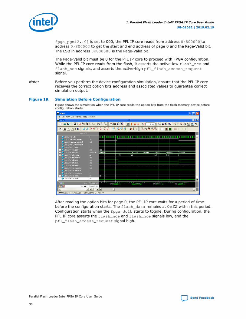
Figure 19. Simulation Before ConfigurationFigure shows the simulation when the PFL IP core reads the option bits from the flash memory device beforeconfiguration starts.
After reading the option bits for page 0, the PFL IP core waits for a period of timebefore the configuration starts. The flash_data remains at 0×ZZ within this period.Configuration starts when the fpga_dclk starts to toggle. During configuration, thePFL IP core asserts the flash_nce and flash_noe signals low, and thepfl_flash_access_request signal high.
1. Parallel Flash Loader Intel® FPGA IP Core User Guide
UG-01082 | 2019.02.19
Parallel Flash Loader Intel FPGA IP Core User Guide Send Feedback
30
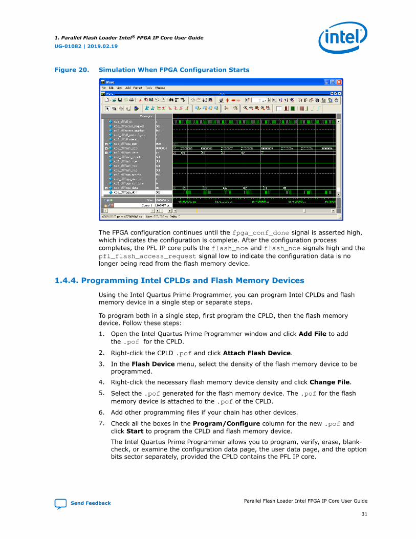
Figure 20. Simulation When FPGA Configuration Starts
The FPGA configuration continues until the fpga_conf_done signal is asserted high,which indicates the configuration is complete. After the configuration processcompletes, the PFL IP core pulls the flash_nce and flash_noe signals high and thepfl_flash_access_request signal low to indicate the configuration data is nolonger being read from the flash memory device.
1.4.4. Programming Intel CPLDs and Flash Memory Devices
Using the Intel Quartus Prime Programmer, you can program Intel CPLDs and flashmemory device in a single step or separate steps.
To program both in a single step, first program the CPLD, then the flash memorydevice. Follow these steps:
1. Open the Intel Quartus Prime Programmer window and click Add File to addthe .pof for the CPLD.
2. Right-click the CPLD .pof and click Attach Flash Device.
3. In the Flash Device menu, select the density of the flash memory device to beprogrammed.
4. Right-click the necessary flash memory device density and click Change File.
5. Select the .pof generated for the flash memory device. The .pof for the flashmemory device is attached to the .pof of the CPLD.
6. Add other programming files if your chain has other devices.
7. Check all the boxes in the Program/Configure column for the new .pof andclick Start to program the CPLD and flash memory device.
The Intel Quartus Prime Programmer allows you to program, verify, erase, blank-check, or examine the configuration data page, the user data page, and the optionbits sector separately, provided the CPLD contains the PFL IP core.
1. Parallel Flash Loader Intel® FPGA IP Core User Guide
UG-01082 | 2019.02.19
Send Feedback Parallel Flash Loader Intel FPGA IP Core User Guide
31
Note: The Intel Quartus Prime programmer erases the flash memory device if youselect the .pof of the flash memory device before programming. To preventthe Intel Quartus Prime Programmer from erasing other sectors in the flashmemory device, select only the pages, .hex data, and option bits.
1.4.4.1. Programming Intel CPLDs and Flash Memory Devices Separately
To program the CPLD and the flash memory devices separately, follow these steps:
1. Open the Intel Quartus Prime Programmer window.
2. Click Add File. The Add Programming File Window dialog box appears.
3. Add the targeted .pof, and click OK.
4. Check the boxes under the Program/Configure column of the .pof.
5. Click Start to program the CPLD.
6. After the programming progress bar reaches 100%, click Auto Detect. Forexample, if you are using dual P30 or P33, the programmer window shows a dualP30 or P33 chain in your setup.
Alternatively, you can add the flash memory device to the programmer manually.Right-click the CPLD .pof and click Select Flash Device. In the Select FlashDevice dialog box, select the device of your choice.
7. Right-click the necessary flash memory device density and click Change File.
Note: You must select the density that is equivalent to the sum of the density oftwo CFI or NAND flash memory devices. For example, if you require two512-Mb CFI flash memory devices, then select CFI 1 Gbit. For more thanone quad SPI flash memory device, select the density that is equivalent tothe sum of all the density of the quad SPI flash memory devices. Forexample, a four quad SPI flash memory devices (128 Mb for each device),the total density is equivalent to 512 Mb. A .pof with 512-Mb flash densityis required to program these quad SPI flash devices. The PFL IP corehandles the 512-Mb .pof programming to the four quad SPI flash memorydevices.
8. Select the .pof generated for the flash memory device. The .pof for the flashmemory device is attached to the .pof of the CPLD.
9. Check the boxes under the Program/Configure column for the added .pof andclick Start to program the flash memory devices.
1.4.5. Defining New CFI Flash Device
The PFL IP core supports Intel-compatible and AMD-compatible flash memory devices.In addition to the supported flash memory devices, you can define the new Intel- orAMD-compatible CFI flash memory device in the PFL-supported flash database usingthe Define new CFI flash memory device feature.
Note: User flash-defined information is stored in the Windows registry. Therefore, you musthave the system administration (administrator) privileges in order to store theparameter in the Define New Flash Device window in the Intel Quartus Primeprogrammer.
1. Parallel Flash Loader Intel® FPGA IP Core User Guide
UG-01082 | 2019.02.19
Parallel Flash Loader Intel FPGA IP Core User Guide Send Feedback
32
To add a new CFI flash memory device to the database or update a CFI flash device inthe database, follow these steps:
1. In the Programmer window, on the Edit menu, select Define New CFI FlashDevice. The Define CFI Flash Device window appears. The following table liststhe three functions available in the Define CFI Flash Device window.
Table 9. Functions of the Define CFI Flash Device Feature
Function Description
New Add new Intel- or AMD-compatible CFI flash memory device into the PFL-supported flash database.
Edit Edit the parameters of the newly added Intel- or AMD-compatible CFI flash memory device in the PFL-supported flash database.
Remove Remove the newly added Intel- or AMD-compatible CFI flash memory device from the PFL-supportedflash database.
2. To add a new CFI flash memory device or edit the parameters of the newly addedCFI flash memory device, select New or Edit. The New CFI Flash Device dialogbox appears.
3. In the New CFI Flash Device dialog box, specify or update the parameters of thenew flash memory device. You can obtain the values for these parameters fromthe datasheet of the flash memory device manufacturer.
Table 10. Parameter Settings for New CFI Flash Device
Parameter Description
CFI flash device name Define the CFI flash name
CFI flash device ID Specify the CFI flash identifier code
CFI flash manufacturer ID Specify the CFI flash manufacturer identification number
CFI flash extended device ID Specify the CFI flash extended device identifier, only applicable for AMD-compatible CFI flash memory device
Flash device is Intel compatible Turn on the option if the CFI flash is Intel compatible
Typical word programming time Typical word programming time value in µs unit
Maximum word programming time Maximum word programming time value in µs unit
Typical buffer programming time Typical buffer programming time value in µs unit
Maximum buffer programming time Maximum buffer programming time value in µs unit
Note: You must specify either the word programming time parameters, bufferprogramming time parameters, or both. Do not leave both programmingtime parameters with the default value of zero.
4. Click OK to save the parameter settings.
5. After you add, update, or remove the new CFI flash memory device, click OK.
Related Information
Supported Flash Memory Devices on page 4
1. Parallel Flash Loader Intel® FPGA IP Core User Guide
UG-01082 | 2019.02.19
Send Feedback Parallel Flash Loader Intel FPGA IP Core User Guide
33
1.4.6. Programming Multiple Flash Memory Devices
The PFL IP core supports multiple-flash programming of as many as 16 flash memorydevices. This feature allows the PFL IP core to connect to multiple flash memorydevices to perform flash programming sequentially. PFL multiple-flash programmingsupports both speed and area mode flash programming. For FPGA configuration, usethe content in the flash memory device that connects to the nCE[0] pin asconfiguration data.
To use the multiple flash programming feature, follow these steps:
1. Select the number of flash memory devices connected to the CPLD in the PFL IPcore parameter editor.
2. Connect the nCE pins of the PFL to the nCE pins of the flash memory device in theblock diagram. Compile the design.
3. Click Auto Detect in the Intel Quartus Prime programmer. The CPLD appears asthe main item, followed by a list of CFI flash memory devices detected assecondary items in the device tree.
4. Attach the flash memory device .pof to each flash memory device.
5. Check the boxes in the Intel Quartus Prime Programmer for the necessaryoperation and click Start.
1.4.7. Creating Jam Files for Intel CPLDs and Flash Memory DeviceProgramming
To use .jam files to program the CPLD and flash memory device, follow these steps:
1. Open the Intel Quartus Prime Programmer window and click Add File to addthe .pof for the CPLD.
2. Right-click the CPLD .pof and click Attach Flash Device.
3. In the Flash Device menu, select the density of the flash memory device to beprogrammed.
4. Right-click the necessary flash memory device density and click Change File.
5. Select the .pof generated for the flash memory device. The .pof for the flashmemory device is attached to the .pof of the CPLD.
6. On the File menu, point to Create/Update and click Create JAM, JBC, SVF, orISF File.
7. Enter a name and select the file format (.jam).
8. Click OK.
Note: Use the .jam files with the Intel Quartus Prime Programmer orquartus_jli executable file.
Related Information
AN425: Using the Command-Line Jam STAPL Solution for Device Programming.Provides more information about the quartus_jli executable.
1. Parallel Flash Loader Intel® FPGA IP Core User Guide
UG-01082 | 2019.02.19
Parallel Flash Loader Intel FPGA IP Core User Guide Send Feedback
34

1.5. PFL IP Core In Embedded Systems
The PFL IP core allows processors, such as the Nios® II processor, to access the flashmemory device while programming flash and configuring an FPGA.
The following figure shows how you can use the PFL IP core to program the flashmemory device and to configure the FPGA with a Nios II processor. The configuredNios II processor uses the non-configuration data stored in the same flash memorydevice.
Figure 21. Single-Device Configuration Using the PFL With the Controller
pfl_nresetpfl_flash_access_granted
flash_addrflash_dataflash_nweflash_nceflash_noe
pfl_flash_access_requestfpga_conf_done
fpga_nstatusfpga_nconfigfpga_data
fpga_dclk
nRPnWP
ADDRDATAnWEnCEnOE
WP#/ACCBYTE#
VCC10kΩ
VCC
FPGACPLDCFI Flash 10kΩ
VCC10kΩVCC VCC
(1)(1)(1)
(2)
Nios II Processor Interface
(3)
(4)
flash_access_grantedext_ram_bus_addrext_ram_bus_datawrite_n_to_ext_flashchip_n_to_ext_flashoutput_n_to_ext_flashWP#/ACCBYTE#
flash_access_request
NC
CONF_DONEnSTATUSnCONFIGDATADCLKnCE nCEO
You must connect the pull-up resistor to a supply that provides an acceptable input signal for the devices. V CC must be high enough to meet the VIH specification of the I/Oon both devices. For example, the Stratix II V IH specification ranges from 1.7 to 3.3 V; therefore, the supply for the pull-up resistor, V CC, must be within 1.7 to 3.3 V to meetthe VIH specification.For PS configuration mode, this is a 1-bit data line. For FPP configuration mode, this is an 8-bit data bus.Do not connect anything to the NC pin (the no connect pin), not even VCC or GND.You can use the Nios II processor in other FPGA, except when you are configuring the FPGA.
(1)
(2)(3)(4)
Figure 22. Relationship Between the Four Sections in the Design Example
CFI FlashMemory
Common FlashInterface
PFL
pfl_flash_access_granted pfl_flash_access_request
FPGA withNIOS II Processor
CPLD
You must configure the Intel FPGA with the Nios II processor when you power-up theboard. You can store the Nios II processor image in the flash memory device and usethe PFL IP core to configure the image to the Intel FPGA. If you store the Nios II
1. Parallel Flash Loader Intel® FPGA IP Core User Guide
UG-01082 | 2019.02.19
Send Feedback Parallel Flash Loader Intel FPGA IP Core User Guide
35
processor image in the same flash memory device you intend to program, do notoverwrite the Nios II processor image when you program the flash memory devicewith other user data.
If you do not want to store the image in the flash memory device, you can store theNios II image in a different storage device, for example an enhanced configuration(EPC) device or an erasable programmable configurable serial (EPCS) memory.
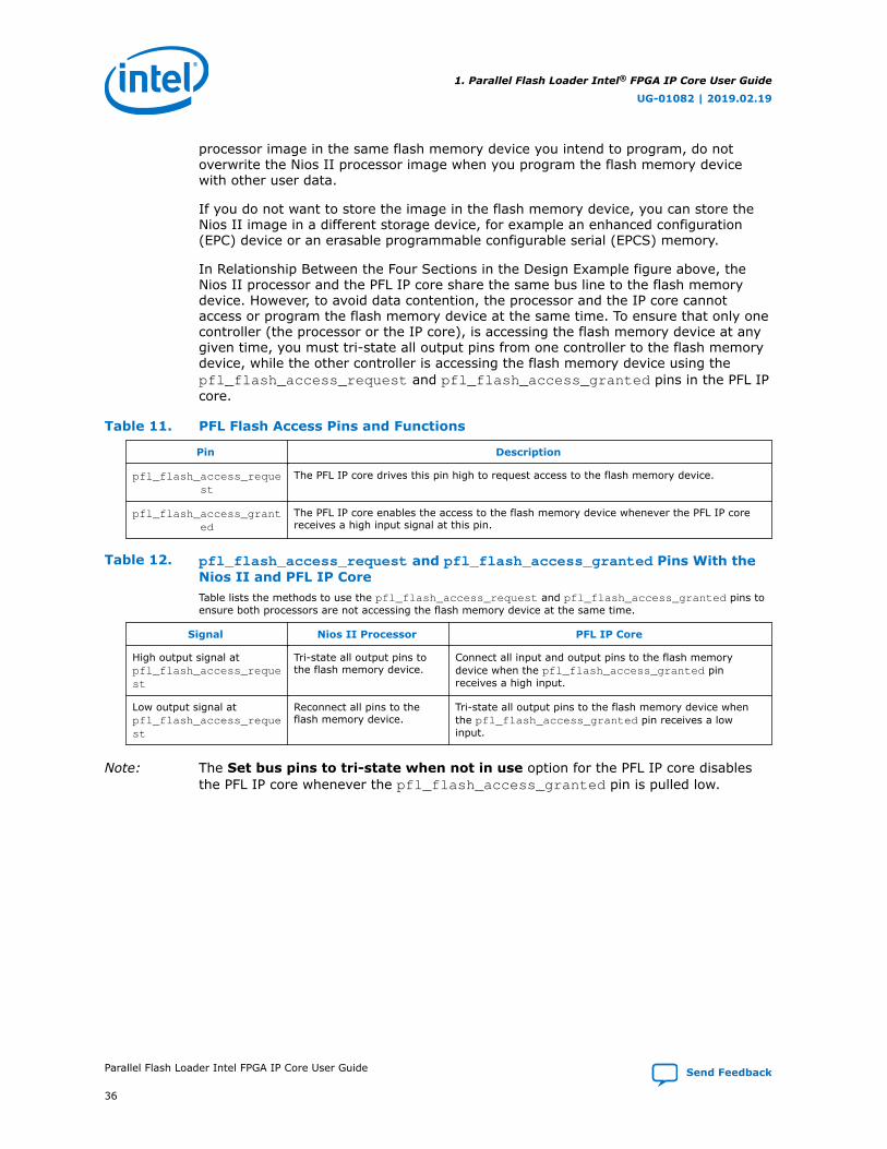
In Relationship Between the Four Sections in the Design Example figure above, theNios II processor and the PFL IP core share the same bus line to the flash memorydevice. However, to avoid data contention, the processor and the IP core cannotaccess or program the flash memory device at the same time. To ensure that only onecontroller (the processor or the IP core), is accessing the flash memory device at anygiven time, you must tri-state all output pins from one controller to the flash memorydevice, while the other controller is accessing the flash memory device using thepfl_flash_access_request and pfl_flash_access_granted pins in the PFL IPcore.
Table 11. PFL Flash Access Pins and Functions
Pin Description
pfl_flash_access_request
The PFL IP core drives this pin high to request access to the flash memory device.
pfl_flash_access_granted
The PFL IP core enables the access to the flash memory device whenever the PFL IP corereceives a high input signal at this pin.
Table 12. pfl_flash_access_request and pfl_flash_access_granted Pins With theNios II and PFL IP CoreTable lists the methods to use the pfl_flash_access_request and pfl_flash_access_granted pins toensure both processors are not accessing the flash memory device at the same time.
Signal Nios II Processor PFL IP Core
High output signal atpfl_flash_access_request
Tri-state all output pins tothe flash memory device.
Connect all input and output pins to the flash memorydevice when the pfl_flash_access_granted pinreceives a high input.
Low output signal atpfl_flash_access_request
Reconnect all pins to theflash memory device.
Tri-state all output pins to the flash memory device whenthe pfl_flash_access_granted pin receives a lowinput.
Note: The Set bus pins to tri-state when not in use option for the PFL IP core disablesthe PFL IP core whenever the pfl_flash_access_granted pin is pulled low.
1. Parallel Flash Loader Intel® FPGA IP Core User Guide
UG-01082 | 2019.02.19
Parallel Flash Loader Intel FPGA IP Core User Guide Send Feedback
36
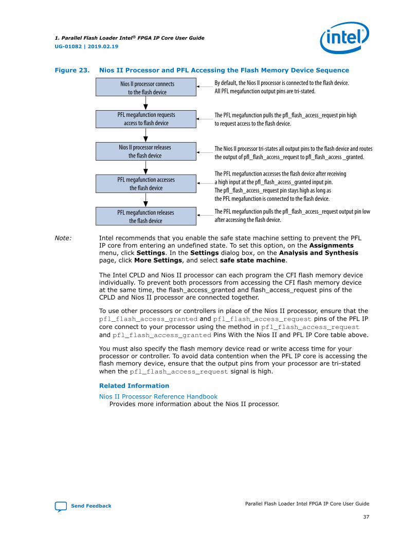
Figure 23. Nios II Processor and PFL Accessing the Flash Memory Device Sequence
Nios II processor connectsto the flash device
The PFL megafunction pulls the pfl_flash_access_request pin highto request access to the flash device.
PFL megafunction requestsaccess to flash device
Nios II processor releasesthe flash device
PFL megafunction accessesthe flash device
PFL megafunction releasesthe flash device
By default, the Nios II processor is connected to the flash device. All PFL megafunction output pins are tri-stated.
The Nios II processor tri-states all output pins to the flash device and routesthe output of pfl_flash_access_request to pfl_flash_access _granted.
The PFL megafunction accesses the flash device after receivinga high input at the pfl_flash_access_granted input pin.The pfl_flash_access_request pin stays high as long asthe PFL megafunction is connected to the flash device.
The PFL megafunction pulls the pfl_flash_access_request output pin lowafter accessing the flash device.
Note: Intel recommends that you enable the safe state machine setting to prevent the PFLIP core from entering an undefined state. To set this option, on the Assignmentsmenu, click Settings. In the Settings dialog box, on the Analysis and Synthesispage, click More Settings, and select safe state machine.
The Intel CPLD and Nios II processor can each program the CFI flash memory deviceindividually. To prevent both processors from accessing the CFI flash memory deviceat the same time, the flash_access_granted and flash_access_request pins of theCPLD and Nios II processor are connected together.
To use other processors or controllers in place of the Nios II processor, ensure that thepfl_flash_access_granted and pfl_flash_access_request pins of the PFL IPcore connect to your processor using the method in pfl_flash_access_requestand pfl_flash_access_granted Pins With the Nios II and PFL IP Core table above.
You must also specify the flash memory device read or write access time for yourprocessor or controller. To avoid data contention when the PFL IP core is accessing theflash memory device, ensure that the output pins from your processor are tri-statedwhen the pfl_flash_access_request signal is high.
Related Information
Nios II Processor Reference HandbookProvides more information about the Nios II processor.
1. Parallel Flash Loader Intel® FPGA IP Core User Guide
UG-01082 | 2019.02.19
Send Feedback Parallel Flash Loader Intel FPGA IP Core User Guide
37
1.6. Third-party Programmer Support
You can program the flash memory using a third-party programmer instead of usingParallel Flash Loader Intel FPGA IP core. To program using third-party programmer,you need to convert the .pof to an .rbf by following the steps below:
1. Compile and generate a .pof file for the flash memory device.
2. Convert .pof file to .hexout file using the following command:
quartus_cpf -c <pof_file_base_name>.pof <hex_file_base_name>.hexout
3. Convert .hexout file created above to .rbf using the nios2-elf-objcopycommand on Nios II Command Shell:
nios2-elf-objcopy –I ihex –O binary <input file>.hexout <output file>.rbf
Related Information
• Programming Flash Memory on page 8
• NIOS II Command-Line ToolsProvides more information on the nios2-elf-objcopy command.
1.7. Parameters
Table 13. PFL General Parameters
Options Value Description
Operating mode • Flash Programming and FPGAConfiguration
• Flash Programming• FPGA Configuration
Specifies the operating mode of flash programming and FPGAconfiguration control in one IP core or separate these functionsinto individual blocks and functionality.
Targeted flashdevice
• CFI Parallel Flash• Altera Active Serial ×4• Quad SPI Flash• NAND Flash
Specifies the flash memory device connected to the PFL IPcore.
Tri-state flashbus
On or Off Allows the PFL IP core to tri-state all pins interfacing with theflash memory device when the PFL IP core does not require anaccess to the flash memory.
Table 14. PFL Flash Interface Setting Parameters
Options Value Description
Number of flashdevices used
• CFI Parallel Flash: 1–16• Altera Active Serial ×4: 1, 2, 4, 8• Quad SPI Flash: 1, 2, 4, 8• NAND Flash: 1
Specifies the number of flash memory devices connected to thePFL IP core.
Largest flashdensity
• CFI Parallel Flash: 8 Mbit–2 Gbit• NAND Flash: 512 Mbit• 1 Gbit - Micron (MT29)• Altera Active Serial x4: EPCQ 256
Mbit
Specifies the density of the flash memory device to beprogrammed or used for FPGA configuration. If you have morethan one flash memory device connected to the PFL IP core,specify the largest flash memory device density.For dual mode CFI and NAND flash devices, select the densitythat is equivalent to the sum of the density of two CFI flashes.For example, if you use two 512-Mb CFI flashes, you mustselect CFI 1 Gbit. (Available only if you select CFI ParallelFlash or NAND Flash.)
continued...
1. Parallel Flash Loader Intel® FPGA IP Core User Guide
UG-01082 | 2019.02.19
Parallel Flash Loader Intel FPGA IP Core User Guide Send Feedback
38
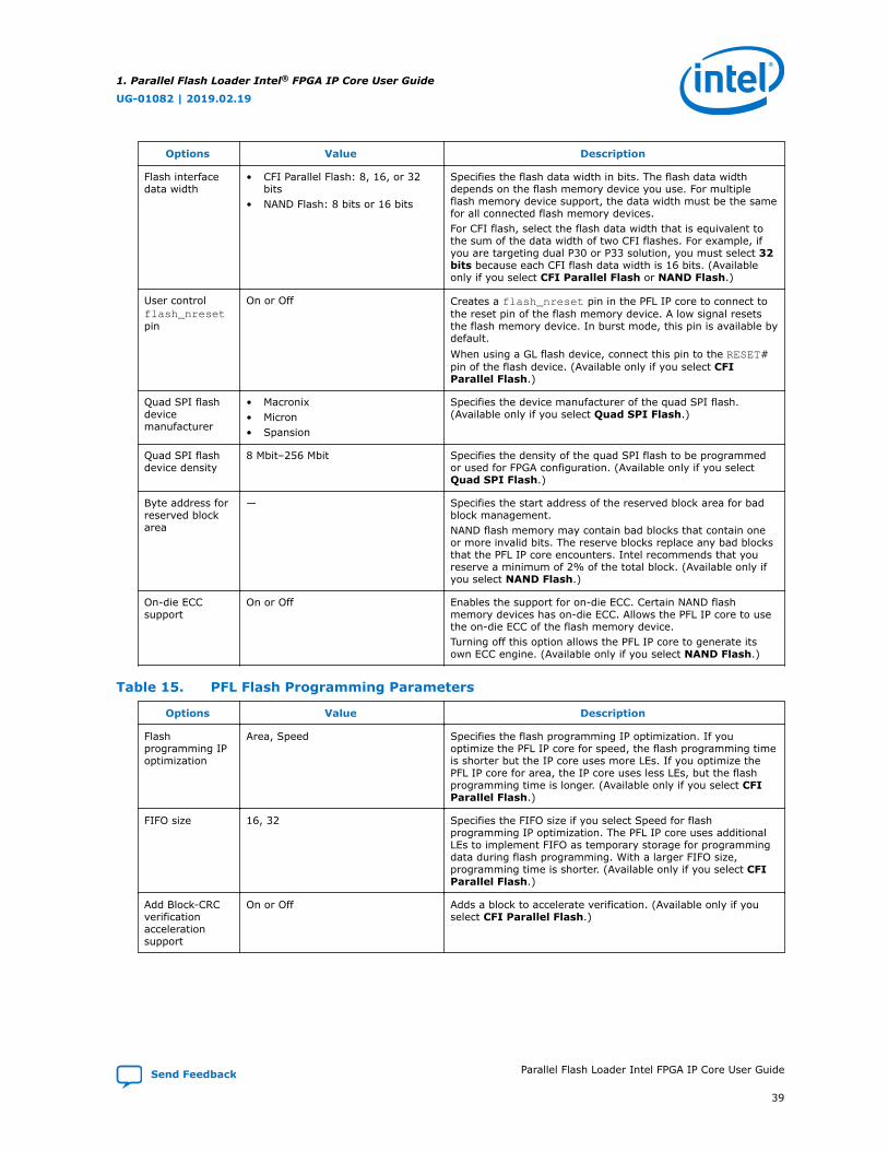
Options Value Description
Flash interfacedata width
• CFI Parallel Flash: 8, 16, or 32bits
• NAND Flash: 8 bits or 16 bits
Specifies the flash data width in bits. The flash data widthdepends on the flash memory device you use. For multipleflash memory device support, the data width must be the samefor all connected flash memory devices.For CFI flash, select the flash data width that is equivalent tothe sum of the data width of two CFI flashes. For example, ifyou are targeting dual P30 or P33 solution, you must select 32bits because each CFI flash data width is 16 bits. (Availableonly if you select CFI Parallel Flash or NAND Flash.)
User controlflash_nresetpin
On or Off Creates a flash_nreset pin in the PFL IP core to connect tothe reset pin of the flash memory device. A low signal resetsthe flash memory device. In burst mode, this pin is available bydefault.When using a GL flash device, connect this pin to the RESET#pin of the flash device. (Available only if you select CFIParallel Flash.)
Quad SPI flashdevicemanufacturer
• Macronix• Micron• Spansion
Specifies the device manufacturer of the quad SPI flash.(Available only if you select Quad SPI Flash.)
Quad SPI flashdevice density
8 Mbit–256 Mbit Specifies the density of the quad SPI flash to be programmedor used for FPGA configuration. (Available only if you selectQuad SPI Flash.)
Byte address forreserved blockarea
— Specifies the start address of the reserved block area for badblock management.NAND flash memory may contain bad blocks that contain oneor more invalid bits. The reserve blocks replace any bad blocksthat the PFL IP core encounters. Intel recommends that youreserve a minimum of 2% of the total block. (Available only ifyou select NAND Flash.)
On-die ECCsupport
On or Off Enables the support for on-die ECC. Certain NAND flashmemory devices has on-die ECC. Allows the PFL IP core to usethe on-die ECC of the flash memory device.Turning off this option allows the PFL IP core to generate itsown ECC engine. (Available only if you select NAND Flash.)
Table 15. PFL Flash Programming Parameters
Options Value Description
Flashprogramming IPoptimization
Area, Speed Specifies the flash programming IP optimization. If youoptimize the PFL IP core for speed, the flash programming timeis shorter but the IP core uses more LEs. If you optimize thePFL IP core for area, the IP core uses less LEs, but the flashprogramming time is longer. (Available only if you select CFIParallel Flash.)
FIFO size 16, 32 Specifies the FIFO size if you select Speed for flashprogramming IP optimization. The PFL IP core uses additionalLEs to implement FIFO as temporary storage for programmingdata during flash programming. With a larger FIFO size,programming time is shorter. (Available only if you select CFIParallel Flash.)
Add Block-CRCverificationaccelerationsupport
On or Off Adds a block to accelerate verification. (Available only if youselect CFI Parallel Flash.)
1. Parallel Flash Loader Intel® FPGA IP Core User Guide
UG-01082 | 2019.02.19
Send Feedback Parallel Flash Loader Intel FPGA IP Core User Guide
39
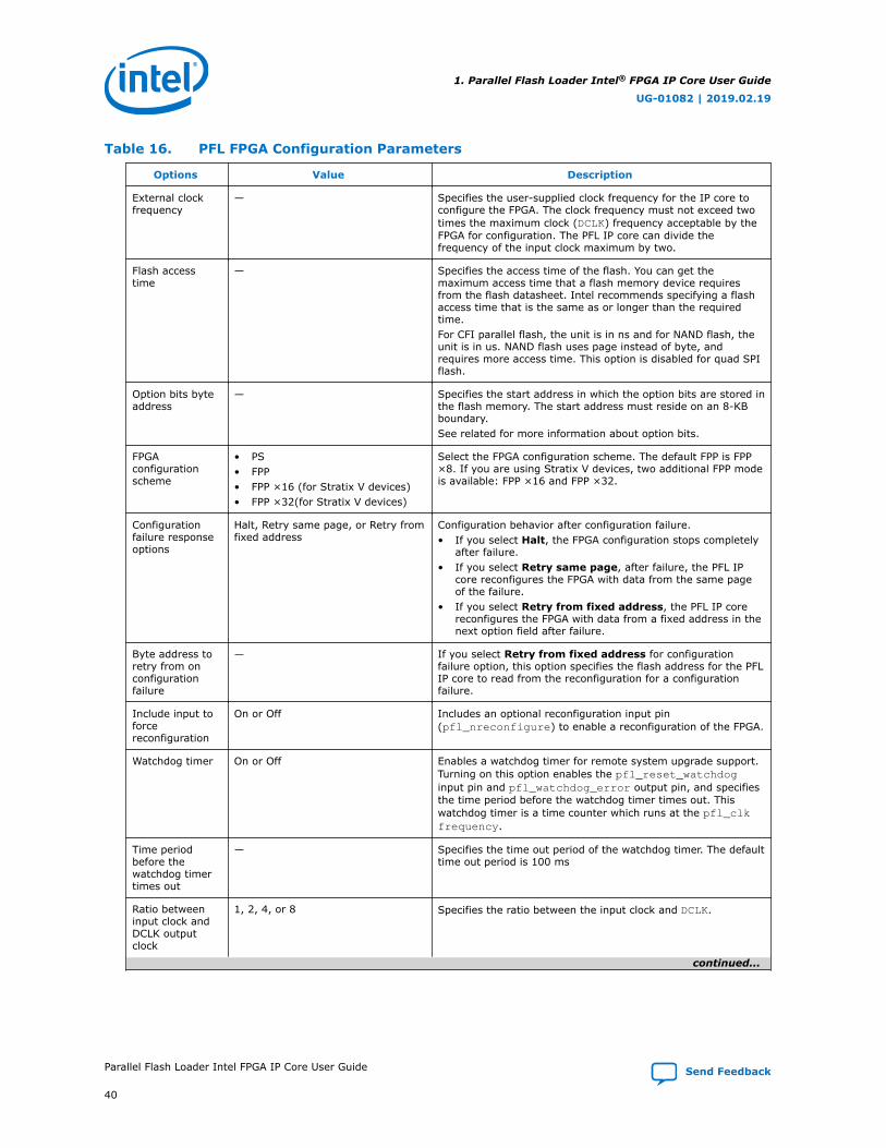
Table 16. PFL FPGA Configuration Parameters
Options Value Description
External clockfrequency
— Specifies the user-supplied clock frequency for the IP core toconfigure the FPGA. The clock frequency must not exceed twotimes the maximum clock (DCLK) frequency acceptable by theFPGA for configuration. The PFL IP core can divide thefrequency of the input clock maximum by two.
Flash accesstime
— Specifies the access time of the flash. You can get themaximum access time that a flash memory device requiresfrom the flash datasheet. Intel recommends specifying a flashaccess time that is the same as or longer than the requiredtime.For CFI parallel flash, the unit is in ns and for NAND flash, theunit is in us. NAND flash uses page instead of byte, andrequires more access time. This option is disabled for quad SPIflash.
Option bits byteaddress
— Specifies the start address in which the option bits are stored inthe flash memory. The start address must reside on an 8-KBboundary.See related for more information about option bits.
FPGAconfigurationscheme
• PS• FPP• FPP ×16 (for Stratix V devices)• FPP ×32(for Stratix V devices)
Select the FPGA configuration scheme. The default FPP is FPP×8. If you are using Stratix V devices, two additional FPP modeis available: FPP ×16 and FPP ×32.
Configurationfailure responseoptions
Halt, Retry same page, or Retry fromfixed address
Configuration behavior after configuration failure.• If you select Halt, the FPGA configuration stops completely
after failure.• If you select Retry same page, after failure, the PFL IP
core reconfigures the FPGA with data from the same pageof the failure.
• If you select Retry from fixed address, the PFL IP corereconfigures the FPGA with data from a fixed address in thenext option field after failure.
Byte address toretry from onconfigurationfailure
— If you select Retry from fixed address for configurationfailure option, this option specifies the flash address for the PFLIP core to read from the reconfiguration for a configurationfailure.
Include input toforcereconfiguration
On or Off Includes an optional reconfiguration input pin(pfl_nreconfigure) to enable a reconfiguration of the FPGA.
Watchdog timer On or Off Enables a watchdog timer for remote system upgrade support.Turning on this option enables the pfl_reset_watchdoginput pin and pfl_watchdog_error output pin, and specifiesthe time period before the watchdog timer times out. Thiswatchdog timer is a time counter which runs at the pfl_clkfrequency.
Time periodbefore thewatchdog timertimes out
— Specifies the time out period of the watchdog timer. The defaulttime out period is 100 ms
Ratio betweeninput clock andDCLK outputclock
1, 2, 4, or 8 Specifies the ratio between the input clock and DCLK.
continued...
1. Parallel Flash Loader Intel® FPGA IP Core User Guide
UG-01082 | 2019.02.19
Parallel Flash Loader Intel FPGA IP Core User Guide Send Feedback
40
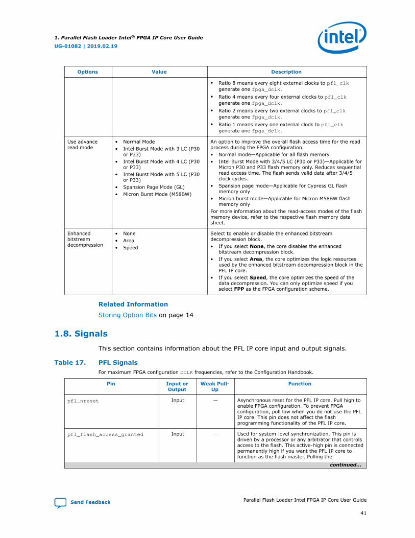
Options Value Description
• Ratio 8 means every eight external clocks to pfl_clkgenerate one fpga_dclk.
• Ratio 4 means every four external clocks to pfl_clkgenerate one fpga_dclk.
• Ratio 2 means every two external clocks to pfl_clkgenerate one fpga_dclk.
• Ratio 1 means every one external clock to pfl_clkgenerate one fpga_dclk.
Use advanceread mode
• Normal Mode• Intel Burst Mode with 3 LC (P30
or P33)• Intel Burst Mode with 4 LC (P30
or P33)• Intel Burst Mode with 5 LC (P30
or P33)• Spansion Page Mode (GL)• Micron Burst Mode (M58BW)
An option to improve the overall flash access time for the readprocess during the FPGA configuration.• Normal mode—Applicable for all flash memory• Intel Burst Mode with 3/4/5 LC (P30 or P33)—Applicable for
Micron P30 and P33 flash memory only. Reduces sequentialread access time. The flash sends valid data after 3/4/5clock cycles.
• Spansion page mode—Applicable for Cypress GL flashmemory only
• Micron burst mode—Applicable for Micron M58BW flashmemory only
For more information about the read-access modes of the flashmemory device, refer to the respective flash memory datasheet.
Enhancedbitstreamdecompression
• None• Area• Speed
Select to enable or disable the enhanced bitstreamdecompression block.• If you select None, the core disables the enhanced
bitstream decompression block.• If you select Area, the core optimizes the logic resources
used by the enhanced bitstream decompression block in thePFL IP core.
• If you select Speed, the core optimizes the speed of thedata decompression. You can only optimize speed if youselect FPP as the FPGA configuration scheme.
Related Information
Storing Option Bits on page 14
1.8. Signals
This section contains information about the PFL IP core input and output signals.
Table 17. PFL SignalsFor maximum FPGA configuration DCLK frequencies, refer to the Configuration Handbook.
Pin Input orOutput
Weak Pull-Up
Function
pfl_nreset Input — Asynchronous reset for the PFL IP core. Pull high toenable FPGA configuration. To prevent FPGAconfiguration, pull low when you do not use the PFLIP core. This pin does not affect the flashprogramming functionality of the PFL IP core.
pfl_flash_access_granted Input — Used for system-level synchronization. This pin isdriven by a processor or any arbitrator that controlsaccess to the flash. This active-high pin is connectedpermanently high if you want the PFL IP core tofunction as the flash master. Pulling the
continued...
1. Parallel Flash Loader Intel® FPGA IP Core User Guide
UG-01082 | 2019.02.19
Send Feedback Parallel Flash Loader Intel FPGA IP Core User Guide
41
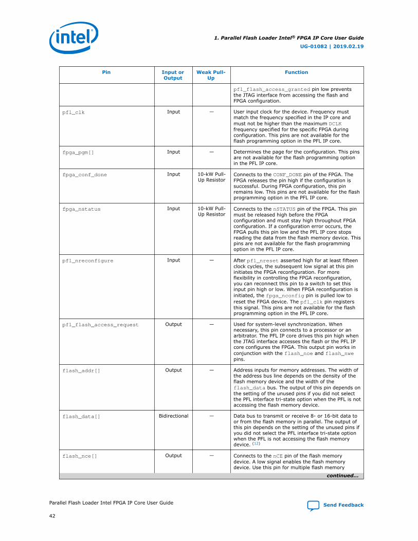
Pin Input orOutput
Weak Pull-Up
Function
pfl_flash_access_granted pin low preventsthe JTAG interface from accessing the flash andFPGA configuration.
pfl_clk Input — User input clock for the device. Frequency mustmatch the frequency specified in the IP core andmust not be higher than the maximum DCLKfrequency specified for the specific FPGA duringconfiguration. This pins are not available for theflash programming option in the PFL IP core.
fpga_pgm[] Input — Determines the page for the configuration. This pinsare not available for the flash programming optionin the PFL IP core.
fpga_conf_done Input 10-kW Pull-Up Resistor
Connects to the CONF_DONE pin of the FPGA. TheFPGA releases the pin high if the configuration issuccessful. During FPGA configuration, this pinremains low. This pins are not available for the flashprogramming option in the PFL IP core.
fpga_nstatus Input 10-kW Pull-Up Resistor
Connects to the nSTATUS pin of the FPGA. This pinmust be released high before the FPGAconfiguration and must stay high throughout FPGAconfiguration. If a configuration error occurs, theFPGA pulls this pin low and the PFL IP core stopsreading the data from the flash memory device. Thispins are not available for the flash programmingoption in the PFL IP core.
pfl_nreconfigure Input — After pfl_nreset asserted high for at least fifteenclock cycles, the subsequent low signal at this pininitiates the FPGA reconfiguration. For moreflexibility in controlling the FPGA reconfiguration,you can reconnect this pin to a switch to set thisinput pin high or low. When FPGA reconfiguration isinitiated, the fpga_nconfig pin is pulled low toreset the FPGA device. The pfl_clk pin registersthis signal. This pins are not available for the flashprogramming option in the PFL IP core.
pfl_flash_access_request Output — Used for system-level synchronization. Whennecessary, this pin connects to a processor or anarbitrator. The PFL IP core drives this pin high whenthe JTAG interface accesses the flash or the PFL IPcore configures the FPGA. This output pin works inconjunction with the flash_noe and flash_nwepins.
flash_addr[] Output — Address inputs for memory addresses. The width ofthe address bus line depends on the density of theflash memory device and the width of theflash_data bus. The output of this pin depends onthe setting of the unused pins if you did not selectthe PFL interface tri-state option when the PFL is notaccessing the flash memory device.
flash_data[] Bidirectional — Data bus to transmit or receive 8- or 16-bit data toor from the flash memory in parallel. The output ofthis pin depends on the setting of the unused pins ifyou did not select the PFL interface tri-state optionwhen the PFL is not accessing the flash memorydevice. (12)
flash_nce[] Output — Connects to the nCE pin of the flash memorydevice. A low signal enables the flash memorydevice. Use this pin for multiple flash memory
continued...
1. Parallel Flash Loader Intel® FPGA IP Core User Guide
UG-01082 | 2019.02.19
Parallel Flash Loader Intel FPGA IP Core User Guide Send Feedback
42
Pin Input orOutput
Weak Pull-Up
Function
device support. The flash_nce pin is connected toeach nCE pin of all the connected flash memorydevices. The width of this port depends on thenumber of flash memory devices in the chain.
flash_nwe Output — Connects to the nWE pin of the flash memorydevice. A low signal enables write operation to theflash memory device.
flash_noe Output — Connects to the nOE pin of the flash memorydevice. A low signal enables the outputs of the flashmemory device during a read operation.
flash_clk Output — Used for burst mode. Connects to the CLK input pinof the flash memory device. The active edges of CLKincrement the flash memory device internal addresscounter. The flash_clk frequency is half of thepfl_clk frequency in burst mode for single CFIflash. In dual P30 or P33 CFI flash solution, theflash_clk frequency runs at a quarter of thepfl_clk frequency. Use this pin for burst modeonly. Do not connect these pins from the flashmemory device to the CPLD device if you are notusing burst mode.
flash_nadv Output — Used for burst mode. Connects to the address validinput pin of the flash memory device. Use this signalfor latching the start address. Use this pin for burstmode only. Do not connect these pins from the flashmemory device to the CPLD device if you are notusing burst mode.
flash_nreset Output — Connects to the reset pin of the flash memorydevice. A low signal resets the flash memory device.
fpga_data[] Output — Data output from the flash to the FPGA deviceduring configuration. For PS mode, this is a 1-bitbus fpga_data[0] data line. For FPP mode, this isan 8-bit fpga_data[7..0] data bus. This pins arenot available for the flash programming option inthe PFL IP core.
fpga_dclk Output — Connects to the DCLK pin of the FPGA. Clock inputdata to the FPGA device during configuration. Thispins are not available for the flash programmingoption in the PFL IP core.
fpga_nconfig Open DrainOutput
10-kW Pull-Up Resistor
Connects to the nCONFIG pin of the FPGA. A lowpulse resets the FPGA and initiates configuration.This pins are not available for the flashprogramming option in the PFL IP core. (12)
flash_sck[] Output — Clock source for flash data read operation. Connectsto the CLK input pin of the quad SPI flash. If youuse more than one quad SPI flash, connect this pinto the CLK input of all the quad SPI flashes. Thewidth of the port is equivalent to the number ofquad SPI flash in the chain.
continued...
(12) Intel recommends not inserting logic between the PFL pins and the CPLD I/O pins, especiallyon the flash_data and fpga_nconfig pins.
1. Parallel Flash Loader Intel® FPGA IP Core User Guide
UG-01082 | 2019.02.19
Send Feedback Parallel Flash Loader Intel FPGA IP Core User Guide
43
Pin Input orOutput
Weak Pull-Up
Function
flash_ncs[] Output — Connects to the ncs pin of the quad SPI flash. If youuse more than one quad SPI flash, connect this pinto the ncs pin of all the quad SPI flashes. The widthof this port is equivalent to the number of quad SPIflashes in the chain.
flash_io0[] Bidirectional — The first bit of the data bus to or from the quad SPIflash. If you use more than one quad SPI flash,connect this pin to the first bit of the data bus of allthe quad SPI flashes. The width of this port isequivalent to the number of quad SPI flashes in thechain.
flash_io1[] Bidirectional — The second bit of the data bus to or from the quadSPI flash. If you use more than one quad SPI flash,connect this pin to the second bit of the data bus ofall the quad SPI flashes. The width of this port isequivalent to the number of quad SPI flashes in thechain.
flash_io2[] Bidirectional — The third bit of the data bus to or from the quad SPIflash. If you use more than one quad SPI flash,connect this pin to the third bit of the data bus of allthe quad SPI flashes. The width of this port isequivalent to the number of quad SPI flashes in thechain.
flash_io3[] Bidirectional — The fourth bit of the data bus to or from the quadSPI flash. If you use more than one quad SPI flash,connect this pin to the fourth bit of the data bus ofall the quad SPI flashes. The width of this port isequivalent to the number of quad SPI flashes in thechain.
pfl_reset_watchdog Input — A toggle signal to reset the watchdog timer beforethe watchdog timer times out. Hold the signal highor low for at least two clock cycles of the pfl_clkfrequency to correctly reset the watchdog timer.
pfl_watchdog_error Output — A high signal indicates an error to the watchdogtimer.
1.9. Specifications
This section provides the equations to estimate the time for reconfiguring the FPGAwith the PFL IP core.
The equations in the following table assume the following definitions:
• Cflash is the number of clock cycles required to read from flash memory.
• Ccfg is the number of input clock cycles to clock out the data (producing betweenone and 16 DCLK cycles, depending on the choice of flash data bus width and FPPor PS mode). Only the larger number between Cflash and Ccfg is important becausereading from the flash and clocking out the data for configuration are performed inparallel.
• Fclk is the input clock frequency to the PFL IP core.
• Taccess is the flash access time.
1. Parallel Flash Loader Intel® FPGA IP Core User Guide
UG-01082 | 2019.02.19
Parallel Flash Loader Intel FPGA IP Core User Guide Send Feedback
44
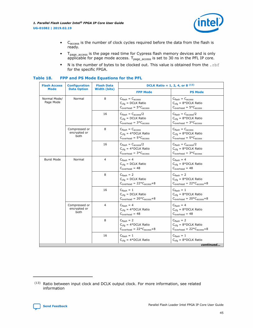
• Caccess is the number of clock cycles required before the data from the flash isready.
• Tpage_access is the page read time for Cypress flash memory devices and is onlyapplicable for page mode access. Tpage_access is set to 30 ns in the PFL IP core.
• N is the number of bytes to be clocked out. This value is obtained from the .rbffor the specific FPGA.
Table 18. FPP and PS Mode Equations for the PFL
Flash AccessMode
ConfigurationData Option
Flash DataWidth (bits)
DCLK Ratio = 1, 2, 4, or 8 (13)
FPP Mode PS Mode
Normal Mode/Page Mode
Normal 8 Cflash = Caccess
Ccfg = DCLK RatioCoverhead = 5*Caccess
Cflash = Caccess
Ccfg = 8*DCLK RatioCoverhead = 5*Caccess
16 Cflash = Caccess/2Ccfg = DCLK RatioCoverhead = 3*Caccess
Cflash = Caccess/2Ccfg = 8*DCLK RatioCoverhead = 3*Caccess
Compressed orencrypted or
both
8 Cflash = Caccess
Ccfg = 4*DCLK RatioCoverhead = 5*Caccess
Cflash = Caccess
Ccfg = 8*DCLK RatioCoverhead = 5*Caccess
16 Cflash = Caccess/2Ccfg = 4*DCLK RatioCoverhead = 3*Caccess
Cflash = Caccess/2Ccfg = 8*DCLK RatioCoverhead = 3*Caccess
Burst Mode Normal 4 Cflash = 4Ccfg = DCLK RatioCoverhead = 48
Cflash = 4Ccfg = 8*DCLK RatioCoverhead = 48
8 Cflash = 2Ccfg = DCLK RatioCoverhead = 22*Caccess+8
Cflash = 2Ccfg = 8*DCLK RatioCoverhead = 22*Caccess+8
16 Cflash = 1Ccfg = DCLK RatioCoverhead = 20*Caccess+8
Cflash = 1Ccfg = 8*DCLK RatioCoverhead = 20*Caccess+8
Compressed orencrypted or
both
4 Cflash = 4Ccfg = 4*DCLK RatioCoverhead = 48
Cflash = 4Ccfg = 8*DCLK RatioCoverhead = 48
8 Cflash = 2Ccfg = 4*DCLK RatioCoverhead = 22*Caccess+8
Cflash = 2Ccfg = 8*DCLK RatioCoverhead = 22*Caccess+8
16 Cflash = 1Ccfg = 4*DCLK Ratio
Cflash = 1Ccfg = 8*DCLK Ratio
continued...
(13) Ratio between input clock and DCLK output clock. For more information, see relatedinformation
1. Parallel Flash Loader Intel® FPGA IP Core User Guide
UG-01082 | 2019.02.19
Send Feedback Parallel Flash Loader Intel FPGA IP Core User Guide
45
Flash AccessMode
ConfigurationData Option
Flash DataWidth (bits)
DCLK Ratio = 1, 2, 4, or 8 (13)
FPP Mode PS Mode
Coverhead = 20*Caccess+8 Coverhead = 20*Caccess+8
• For Normal Mode and Burst Mode:Caccess = Taccess*Fclk+1Total Clock Cycles (from nRESET asserted high to N bytes of data clocked out)= Coverhead + max(Cflash, Ccfg)*NTotal Configuration Time = Total Clock Cycle/ PFL Input Clock
• For Page ModeCaccess = [(Taccess*Fclk+1) + ((Tpage_access*Fclk+1)*15)]/16Total Clock Cycles (from nRESET asserted high to N bytes of data clocked out)= Coverhead + max (Cflash, Ccfg)*NTotal Configuration Time = Total Clock Cycle/ PFL Input Clock
• For FPP (×8)Total Clock Cycles (from nRESET asserted high to N bytes of data clocked out)Cflash remains the same
• For FPP (×16)Total Clock Cycles (from nRESET asserted high to N word of data clocked out)Cflash = Cflash × 2 (×2 of Cflash from FPP ×8)
• For FPP (×32)Total Clock Cycles (from nRESET asserted high to N double word of data clocked out)Cflash = Cflash × 4 (×4 of Cflash from FPP ×8)
1.9.1. Configuration Time Calculation Examples
The following are the configuration time calculation examples for normal mode, pagemode, and burst mode:
Note: Any reference to the core clock speed of 100 MHz is only an example of theconfiguration time calculation and not a recommendation of the actual clock.
Example 2. Normal Mode
• Normal mode configuration time calculation:
.rbf size for EP2S15 = 577KB = 590,848 Bytes
Configuration mode = FPP without data compression or encryption
Flash access mode = Normal Mode
Flash data bus width = 16 bits
Flash access time = 100 ns
PFL input Clock = 100 MHz
DCLK ratio = 2
(13) Ratio between input clock and DCLK output clock. For more information, see relatedinformation
1. Parallel Flash Loader Intel® FPGA IP Core User Guide
UG-01082 | 2019.02.19
Parallel Flash Loader Intel FPGA IP Core User Guide Send Feedback
46
• Use the following formulas in this calculation:
Caccess = Taccess*Fclk+1
Cflash for Normal Mode = Caccess / 2
Ccfg = 2
Coverhead = 3*Caccess
Total Clock Cycles = Coverhead + max (Cflash, Ccfg)*N
Total Configuration Time = Total Clock Cycle/ PFL Input Clock
• Substitute these values in the following formulas:
Caccess = (100ns * 100MHz) + 1 = 11
Cflash = 11/2 = 5.5
Ccfg = 2
Coverhead = 3*11 = 33
Total Clock Cycles = 33 + 5.5 * 590848 = 3249697
Total Configuration Time at 100 MHz = 3249697/ 100 × 106 = 32.5ms
Example 3. Page Mode
• Page mode configuration time calculation:
.rbf size for EP2S15 = 577 KB = 590,848 Bytes
Configuration mode = FPP without data compression or encryption
Flash access mode = Page Mode
Flash data bus width = 16 bits
Flash access time = 100 ns
PFL input Clock = 100 MHz
DCLK ratio = 2
• Use the following formulas in this calculation:
Tpage_access = 30 ns
Caccess = [(Taccess*Fclk+1) + ((Tpage_access*Fclk+1)*15)]/16
Cflash for Page Mode = Caccess / 2
Ccfg = 2
Coverhead = 3* Caccess
Total Clock Cycles = Coverhead + max (Cflash, Ccfg)*N
Total Configuration Time = Total Clock Cycle/ PFL Input Clock
• Substitute these values in the following formulas:
Caccess = [((100ns * 100 MHz) + 1) + (30ns*100 MHz*15)]/16 = 3.5
Cflash for Page Mode = 3.5/ 2 = 1.75 = 2
Ccfg = 2
Coverhead = 3*3.5 = 10.5
Total Clock Cycles = 10.5 + 2*590848 = 1181706.5
Total Configuration Time at 100 MHz = 1181706.5 / 100 × 106 = 11.82 ms
1. Parallel Flash Loader Intel® FPGA IP Core User Guide
UG-01082 | 2019.02.19
Send Feedback Parallel Flash Loader Intel FPGA IP Core User Guide
47
Example 4. Burst Mode
• Burst mode configuration time calculation:
.rbf size for EP2S15 = 577KB = 590,848 Bytes
Configuration mode = FPP without data compression or encryption
Flash access mode = Burst Mode
Flash data bus width = 16 bits
Flash access time = 100 ns
PFL input Clock = 100 MHz
DCLK ratio = 2
• Use the following formulas in this calculation:
Caccess = Taccess*Fclk+1
Cflash for Burst Mode = 1
Ccfg = 2
Coverhead = 20* Caccess + 8
Total Clock Cycles = Coverhead + max (Cflash, Ccfg)*N
Total Configuration Time = Total Clock Cycle/ PFL Input Clock
• Substitute these values in the following formulas:
Caccess = (100ns * 100 MHz) + 1 = 11
Cflash = 1
Ccfg = 2
Coverhead = (20*11)+8 = 228
Total Clock Cycles = 228 + 2 * 590848 = 1181924
Total Configuration Time at 100 MHz = 1181924 / 100 × 106 = 11.82 ms
1. Parallel Flash Loader Intel® FPGA IP Core User Guide
UG-01082 | 2019.02.19
Parallel Flash Loader Intel FPGA IP Core User Guide Send Feedback
48
Example 5. Single Quad SPI Flash
• Single quad SPI flash configuration time calcualtion
.rbf size for EP2S15 = 577KB = 590,848 Bytes
Configuration mode = FPP without data compression or encryption
Flash access mode = Burst Mode
Flash data bus width = 4 bits (only one quad SPI flash is used)
Flash access time = 100 ns
PFL input Clock = 100 MHz
DCLK ratio = 2
• Use the following formulas in this calculation:
Cflash = 4
Ccfg = 2
Coverhead = 48
Total Clock Cycles = Coverhead + max (Cflash, Ccfg)*N
Total Configuration Time = Total Clock Cycle/ PFL Input Clock
• Substitute these values in the following formulas:
Cflash = 4
Ccfg = 2
Coverhead = 48
Total Clock Cycles = 48 + 4 * 590848 = 2363440
Total Configuration Time at 100 MHz = 2363440 / 100 × 106 = 23.63 ms
Example 6. Four Cascaded Quad SPI Flashes
• Four cascaded quad SPI flashes configuration time calculation:
.rbf size for EP2S15 = 577KB = 590,848 Bytes
Configuration mode = FPP without data compression or encryption
Flash access mode = Burst Mode
Flash data bus width = 16 bits (total bus width for four quad SPI flashes)
Flash access time = 100 ns
PFL input Clock = 100 MHz
DCLK ratio = 2
The configuration time calculation for four cascaded quad SPI flash is identical to theconfiguration time calculation for CFI flash with 16 bit flash data width.
1. Parallel Flash Loader Intel® FPGA IP Core User Guide
UG-01082 | 2019.02.19
Send Feedback Parallel Flash Loader Intel FPGA IP Core User Guide
49
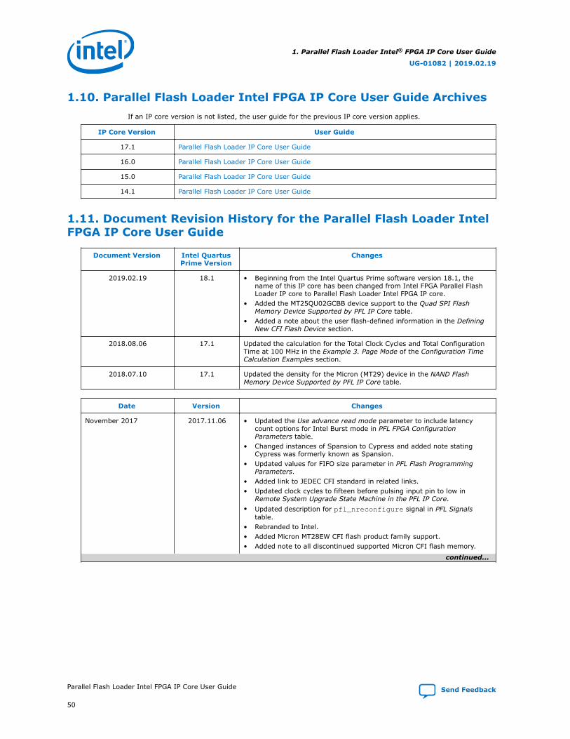
1.10. Parallel Flash Loader Intel FPGA IP Core User Guide ArchivesIf an IP core version is not listed, the user guide for the previous IP core version applies.
IP Core Version User Guide
17.1 Parallel Flash Loader IP Core User Guide
16.0 Parallel Flash Loader IP Core User Guide
15.0 Parallel Flash Loader IP Core User Guide
14.1 Parallel Flash Loader IP Core User Guide
1.11. Document Revision History for the Parallel Flash Loader IntelFPGA IP Core User Guide
Document Version Intel QuartusPrime Version
Changes
2019.02.19 18.1 • Beginning from the Intel Quartus Prime software version 18.1, thename of this IP core has been changed from Intel FPGA Parallel FlashLoader IP core to Parallel Flash Loader Intel FPGA IP core.
• Added the MT25QU02GCBB device support to the Quad SPI FlashMemory Device Supported by PFL IP Core table.
• Added a note about the user flash-defined information in the DefiningNew CFI Flash Device section.
2018.08.06 17.1 Updated the calculation for the Total Clock Cycles and Total ConfigurationTime at 100 MHz in the Example 3. Page Mode of the Configuration TimeCalculation Examples section.
2018.07.10 17.1 Updated the density for the Micron (MT29) device in the NAND FlashMemory Device Supported by PFL IP Core table.
Date Version Changes
November 2017 2017.11.06 • Updated the Use advance read mode parameter to include latencycount options for Intel Burst mode in PFL FPGA ConfigurationParameters table.
• Changed instances of Spansion to Cypress and added note statingCypress was formerly known as Spansion.
• Updated values for FIFO size parameter in PFL Flash ProgrammingParameters.
• Added link to JEDEC CFI standard in related links.• Updated clock cycles to fifteen before pulsing input pin to low in
Remote System Upgrade State Machine in the PFL IP Core.• Updated description for pfl_nreconfigure signal in PFL Signals
table.• Rebranded to Intel.• Added Micron MT28EW CFI flash product family support.• Added note to all discontinued supported Micron CFI flash memory.
continued...
1. Parallel Flash Loader Intel® FPGA IP Core User Guide
UG-01082 | 2019.02.19
Parallel Flash Loader Intel FPGA IP Core User Guide Send Feedback
50

Date Version Changes
• Updated flash_io0[], flash_io1[], flash_io2[] andflash_io3[] from output to bidirectional in PFL Signals table.
• Changed instances of EON Silicon Solution to ESMT and added notestating ESMT was formerly known as EON Silicon Solution.
• Updated Largest flash density parameter description.
October 2016 2016.10.31 • Updated Micron flash in CFI Flash Memory Devices Supported by PFL IPCore.
• Removed FS Spansion flash in Quad SPI Flash Memory DeviceSupported by PFL IP Core.
• Updated parameter value in PFL Flash Interface Setting Parameters.
June 2016 2016.06.01 • Corrected DCLK ratio and Ccfg in Normal Mode and Page Modeexamples.
• Added N25Q256 in Quad SPI Flash Memory Device Supported by PFL IPCore.
• Removed S25FS512S in Quad SPI Flash Memory Device Supported byPFL IP Core.
• Edited Parameters table by breaking grouped tables.• Updated Number of flash devices used and Largest flash density
options in PFL Flash Interface Setting Parameters table
May 2016 2016.05.02 • Changed instances of Quartus II to Quartus Prime.• Added steps to set up PFL simulation using NativeLink and perform
ModelSim simulation.• Corrected constraint type for fpga_data and fpga_dclk.• Corrected DCLK ratio in Normal Mode and Page Mode examples.• Corrected Caccess formula for Page Mode configuration time calculation.• Corrected delay value for flash_data.
June 2015 2015.06.15 Added support for Spansion S25FS256S and S25FS512S.
January 2015 2015.01.23 • Corrected DATA width in PFL IP core With Dual P30 or P33 CFI FlashMemory Devices figure.
• Corrected Spansion part number for S29JL032H and S29JL032H from229JL032H and 229JL032H respectively.
• Added Micron MT28GU512AAA1EGC-0SIT andMT28GU01GAAA1EGC-0SIT
• Added example of programming PFL using command line.• Rearranged the supported flash memory device by grouping device
families.• Added third-party programmer support.
June 2014 2014.06.30 Replaced MegaWizard Plug-In Manager information with IP Catalog.
May 2014 3.2 Updated Table 16 on page 41 to remove Stratix V limitation for theEnhanced bitstream decompression IP core option.
May 2013 3.1 Updated Table 2 on page 5 to add 28F00BP30 and 28F00BP33.
September 2012 3.0 • Updated manufacturer name from Numonyx to Micron.• Updated “Implementing Remote System Upgrade with the PFL IP Core”
on page 22, and “Specifications” on page 49• Updated Table 4 on page 7, Table 10 on page 30, Table 16 on page 41,
Table 17 on page 45, and Table 18 on page 50.• Removed figures.
August 2012 2.1 Updated Table 1.
continued...
1. Parallel Flash Loader Intel® FPGA IP Core User Guide
UG-01082 | 2019.02.19
Send Feedback Parallel Flash Loader Intel FPGA IP Core User Guide
51
Date Version Changes
December 2011 2.0 • Updated “Using Enhanced Bitstream Compression and Decompression”to include reference.
• Updated Table 1 to include Eon Silicon CFI device EN29GL128 and toremove S29GL-N devices.
• Updated Table 2 to include Micron QSPI device N25Q128.• Updated “Specifications”• Updated Table 13 to include FPP x16 and FPP x32 configuration scheme
for Stratix V devices.• Updated Figure 27.• Added Figure 31.• Minor text edits
February 2011 1.1 • Restructured the user guide.• Added information about the new feature for the Quartus II software
10.1 release: Support for NAND flash.
July 2010 1.0 Converted from AN386: Using the Parallel Flash Loader With the Quartus IISoftware.
1. Parallel Flash Loader Intel® FPGA IP Core User Guide
UG-01082 | 2019.02.19
Parallel Flash Loader Intel FPGA IP Core User Guide Send Feedback
52