Embed Size (px)
Citation preview
Altera CorporationAN-386-4.1
May 2008, ver. 4.1
Using the Parallel FlashLoader with the Quartus II
Software
Application Note 386Introduction With the density of FPGAs increasing, the need for larger configuration storage is also increasing. If your system already contains a common flash interface (CFI) flash memory, you can utilize it for the FPGA configuration storage as well. The parallel flash loader (PFL) feature in MAX® II devices provides an efficient method to program CFI flash memory devices through the Joint Test Action Group (JTAG) interface and the logic to control configuration from the flash memory device to the Altera® FPGA. Figure 1 illustrates the PFL feature.
Figure 1. MAX II PFL Feature
Notes to Figure 1: (1) Refer to Table 1 for the list of supported CFI flash devices.(2) Fast Passive Parallel (FPP) and Passive Serial (PS) are configuration schemes that
allow configuration data to be loaded to a target device. FPP allows eight bits of data to be loaded on every clock cycle; PS allows only one bit. For more information about FPP and PS, refer to the Configuration Handbook.
MAX II PFL The two functions of the PFL feature are:
■ Programming the CFI flash device through the MAX II JTAG interface.
■ Controlling Altera FPGA configuration from a CFI flash for Stratix® series, Cyclone® series, APEX™ II, APEX 20K (including APEX 20K, APEX 20KC, and APEX 20KE), Mercury™, ACEX® 1K, and FLEX® 10K (FLEX 10KE and FLEX 10KA) FPGA devices.
CFI FlashMemory
AlteraFPGA
CommonFlashInterface
Passive Serial orFast-Passive Parallel
InterfaceQuartus IISoftwarevia JTAG
(2)
(1)
MAX II CPLD
PFL
1
Using the Parallel Flash Loader with the Quartus II Software
Programming the CFI Flash
The MAX II device operates as the bridge between the JTAG interface and the CFI flash memory parallel address or data interface. Altera configuration devices support programming through the JTAG interface, allowing in-system programming and updates. Standard flash memory devices, however, do not support the JTAG interface and therefore, do not support direct programming through JTAG. With the MAX II device, you can use its JTAG interface to indirectly program the flash memory. The MAX II JTAG block interfaces directly with the logic array when in a special non-test JTAG mode. This mode brings the JTAG chain through the logic array instead of the MAX II boundary scan cells. The PFL feature provides the JTAG interface logic to convert the JTAG stream provided by the Quartus® II software and program CFI flash memory devices connected to the MAX II I/O pins. Figure 2 shows the MAX II device acting as the bridge to program the flash memory through the JTAG interface.
Figure 2. Programming the Flash Memory via the JTAG Interface
Controlling Altera FPGA Configuration from a CFI Flash
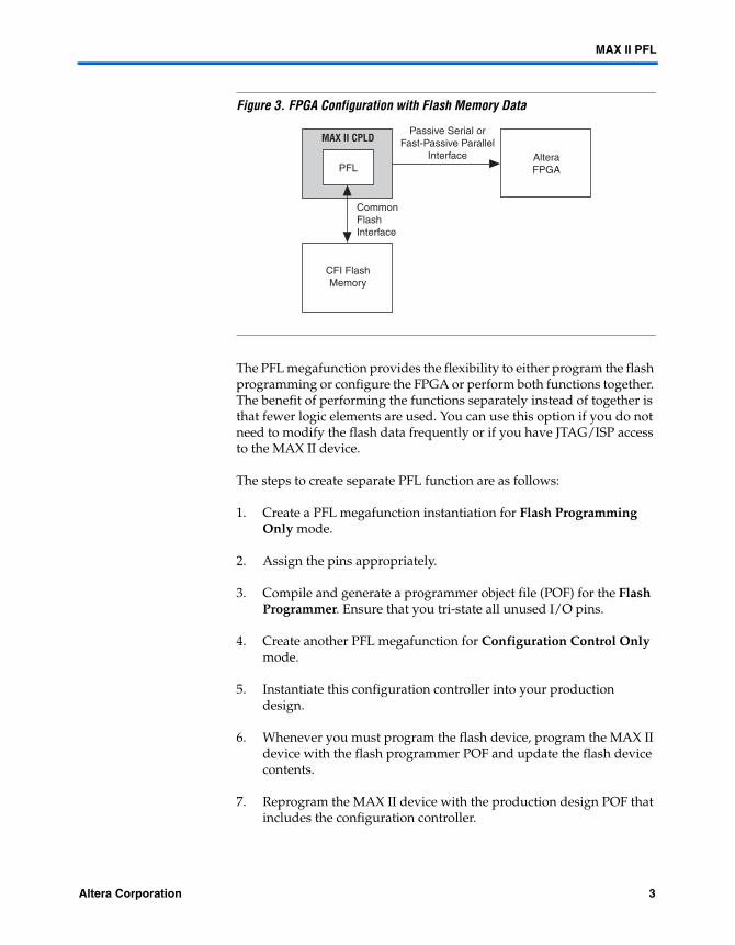
The MAX II device controls the configuration of Altera FPGAs. Unlike dedicated Altera configuration devices, the flash memory device only stores configuration data and does not have the built-in logic to control the FPGA configuration process. The PFL megafunction logic within the MAX II device determines when to start the configuration process, read the data from the flash memory, and configure the Altera FPGA accordingly. Figure 3 shows the MAX II device as the configuration controller for the FPGA.
MAX II CPLD
CFI FlashMemory
AlteraFPGAConfiguration Data
CommonFlashInterface
PFLQuartus IISoftwarevia JTAG
Altera FPGA Not Usedfor Flash Programming
2 Altera Corporation
MAX II PFL
Figure 3. FPGA Configuration with Flash Memory Data
The PFL megafunction provides the flexibility to either program the flash programming or configure the FPGA or perform both functions together. The benefit of performing the functions separately instead of together is that fewer logic elements are used. You can use this option if you do not need to modify the flash data frequently or if you have JTAG/ISP access to the MAX II device.
The steps to create separate PFL function are as follows:
1. Create a PFL megafunction instantiation for Flash Programming Only mode.
2. Assign the pins appropriately.
3. Compile and generate a programmer object file (POF) for the Flash Programmer. Ensure that you tri-state all unused I/O pins.
4. Create another PFL megafunction for Configuration Control Only mode.
5. Instantiate this configuration controller into your production design.
6. Whenever you must program the flash device, program the MAX II device with the flash programmer POF and update the flash device contents.
7. Reprogram the MAX II device with the production design POF that includes the configuration controller.
MAX II CPLD
CFI FlashMemory
AlteraFPGA
CommonFlashInterface
PFL
Passive Serial orFast-Passive Parallel
Interface
Altera Corporation 3
Using the Parallel Flash Loader with the Quartus II Software
Programming the flash with non-Altera data is another benefit of having separate functionality. For example, the flash device contains initialization storage for an application-specific standard product (ASSP). You can use the PFL to program the flash with the initialization data and also create your own design source code to implement the read and initialization control with the MAX II logic.
1 By default, all unused pins are set to ground. If you must keep the FPGA configuration data during flash programming, you must tri-state the FPGA configuration pins common to the MAX II device interface in your flash programming design file.
1 The MAX II device tri-states all I/O pins during the CPLD programming. However, the MAX II device functions as normal and does not tri-state the I/O pins during the flash programming and the FPGA configuration.
Quartus II Software Support
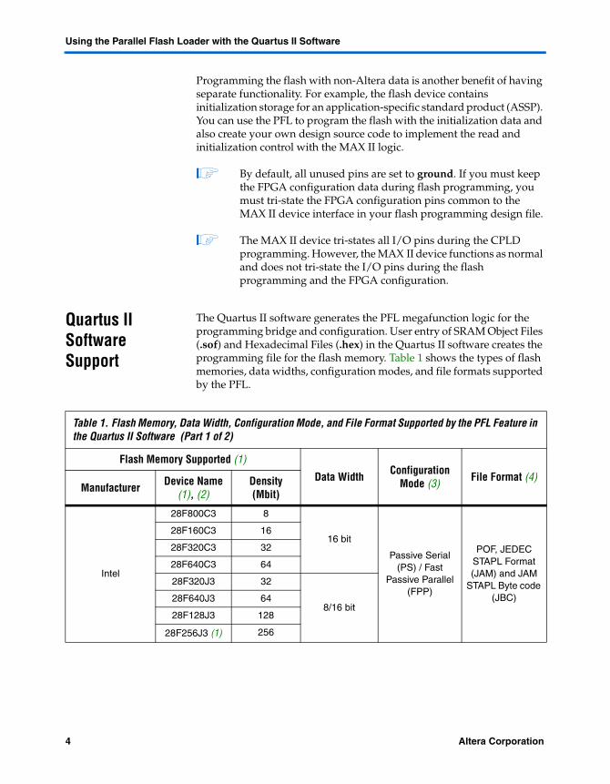
The Quartus II software generates the PFL megafunction logic for the programming bridge and configuration. User entry of SRAM Object Files (.sof) and Hexadecimal Files (.hex) in the Quartus II software creates the programming file for the flash memory. Table 1 shows the types of flash memories, data widths, configuration modes, and file formats supported by the PFL.
Table 1. Flash Memory, Data Width, Configuration Mode, and File Format Supported by the PFL Feature in the Quartus II Software (Part 1 of 2)
Flash Memory Supported (1)
Data Width Configuration Mode (3) File Format (4)
Manufacturer Device Name (1), (2)
Density (Mbit)
Intel
28F800C3 8
16 bit
Passive Serial (PS) / Fast
Passive Parallel (FPP)
POF, JEDEC STAPL Format (JAM) and JAM
STAPL Byte code (JBC)
28F160C3 16
28F320C3 32
28F640C3 64
28F320J3 32
8/16 bit28F640J3 64
28F128J3 128
28F256J3 (1) 256
4 Altera Corporation
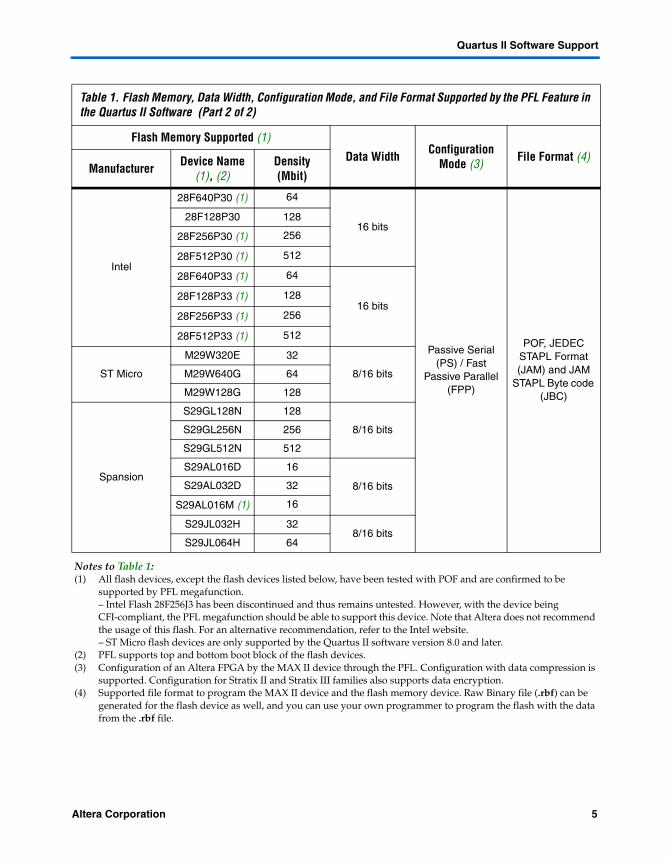
Quartus II Software Support
Intel
28F640P30 (1) 64
16 bits
Passive Serial (PS) / Fast
Passive Parallel (FPP)
POF, JEDEC STAPL Format (JAM) and JAM
STAPL Byte code (JBC)
28F128P30 128
28F256P30 (1) 256
28F512P30 (1) 512
28F640P33 (1) 64
16 bits28F128P33 (1) 128
28F256P33 (1) 256
28F512P33 (1) 512
ST Micro
M29W320E 32
8/16 bits M29W640G 64
M29W128G 128
Spansion
S29GL128N 128
8/16 bitsS29GL256N 256
S29GL512N 512
S29AL016D 16
8/16 bitsS29AL032D 32
S29AL016M (1) 16
S29JL032H 328/16 bits
S29JL064H 64
Notes to Table 1: (1) All flash devices, except the flash devices listed below, have been tested with POF and are confirmed to be
supported by PFL megafunction.– Intel Flash 28F256J3 has been discontinued and thus remains untested. However, with the device being CFI-compliant, the PFL megafunction should be able to support this device. Note that Altera does not recommend the usage of this flash. For an alternative recommendation, refer to the Intel website.– ST Micro flash devices are only supported by the Quartus II software version 8.0 and later.
(2) PFL supports top and bottom boot block of the flash devices.(3) Configuration of an Altera FPGA by the MAX II device through the PFL. Configuration with data compression is
supported. Configuration for Stratix II and Stratix III families also supports data encryption.(4) Supported file format to program the MAX II device and the flash memory device. Raw Binary file (.rbf) can be
generated for the flash device as well, and you can use your own programmer to program the flash with the data from the .rbf file.
Table 1. Flash Memory, Data Width, Configuration Mode, and File Format Supported by the PFL Feature in the Quartus II Software (Part 2 of 2)
Flash Memory Supported (1)
Data Width Configuration Mode (3) File Format (4)
Manufacturer Device Name (1), (2)
Density (Mbit)
Altera Corporation 5
Using the Parallel Flash Loader with the Quartus II Software
The logic element (LE) usage for the PFL varies with different PFL and the Quartus II software settings. The only way to get the exact number on the LE usage is to compile a PFL design with the exact settings, using the Quartus II software.
Page Implementation in Flash POF
The PFL stores configuration data up to a maximum of eight different pages in a CFI flash memory block. A single page is used to configure a single FPGA chain that can contain more than one FPGA (for example, multiple SOFs can be stored in a single page).
The number of pages and the size of a page depend on individual user or design. The total number of pages allowed and the size of each page depend on the density of the flash. These pages allow users to store designs for different FPGA chains or different designs for the same FPGA chain in different pages.
When converting the SOF(s) to a POF, three address modes are available to determine the page address: Block mode, Start mode, and Auto mode.
■ Block mode—Allows you to specify the start and end addresses for the page.
■ Start mode—Allows you to specify only the start address. The start address for each page resides on an 8-KByte boundary, which means that if the first valid start address is 0x000000, the next valid start address must be an increment of 0x2000.
■ Auto mode—Allows the Quartus II software to automatically determine the start address of the page. The Quartus II software aligns the pages on a 128-KByte boundary; for example, if the first valid start address is 0x000000, the next valid start address must be an increment of 0x20000.
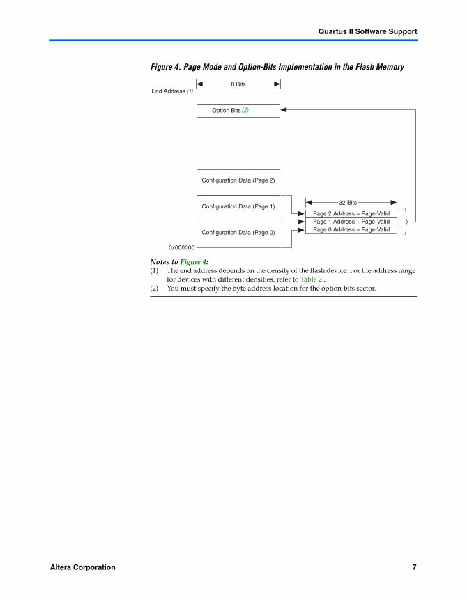
The option-bit sector stores the start address for each page and the Page-Valid bits, indicating whether each page is successfully programmed. The programmer programs the Page-Valid bits after successfully programming the pages. Always store the option-bits in unused address locations in the flash memory. The start address for the option-bit sector must reside on an 8-KByte boundary. You must specify the start address for the option-bit sector when converting the SOF(s) to the POF, as well as when creating the PFL megafunction. This procedure is detailed in “Instantiating the PFL Megafunction in Quartus II Software” on page 30 and “Converting the SOF(s) to a POF for the Flash Device” on page 34. Figure 4 shows the page mode and option-bits implementation in the CFI flash memory.
6 Altera Corporation
Quartus II Software Support
Figure 4. Page Mode and Option-Bits Implementation in the Flash Memory
Notes to Figure 4:(1) The end address depends on the density of the flash device. For the address range
for devices with different densities, refer to Table 2 .(2) You must specify the byte address location for the option-bits sector.
Option Bits
Configuration Data (Page 2)
Configuration Data (Page 1)
Configuration Data (Page 0)
Page 2 Address + Page-ValidPage 1 Address + Page-ValidPage 0 Address + Page-Valid
End Address
0x000000
8 Bits
(2)
(1)
32 Bits
Altera Corporation 7
Using the Parallel Flash Loader with the Quartus II Software
Bits 0 to 11 for the Page Start Address are all set to zeros and are not stored as option bits. Figure 5 shows how the start address and Page-Valid bit for each page are stored in the option-bit sector. Table 2 shows the byte address range for CFI devices with different densities.
Figure 5. Page Start Address, End Address, and Page-Valid Bit Stored as Option Bits
Note to Figure 5:(1) For flash byte addressing mode.
Table 2. Byte Address Range
CFI Device (Mbit) Address Range
8 0x0000000 – 0x00FFFFF
16 0x0000000 – 0x01FFFFF
32 0x0000000 – 0x03FFFFF
64 0x0000000 – 0x07FFFFF
128 0x0000000 – 0x0FFFFFF
256 0x0000000 – 0x1FFFFFF
512 0x0000000 – 0x3FFFFFF
Page Start Address [19:13] Page-Valid
Bit 7...Bit 1 Bit 0
Page Start Address [27:20]
Bit 7...Bit 0
0x002000
0x002001
Page End Address [19:13]
Bit 7...Bit 1
0x002002
Page End Address [27:20]
Bit 7...Bit 0
0x002003
(1)
8 Altera Corporation
Input and Output Signals for the PFL
Input and Output Signals for the PFL
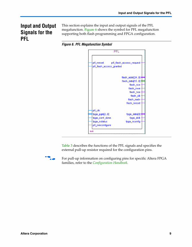
This section explains the input and output signals of the PFL megafunction. Figure 6 shows the symbol for PFL megafunction supporting both flash programming and FPGA configuration.
Figure 6. PFL Megafunction Symbol
Table 3 describes the functions of the PFL signals and specifies the external pull-up resistor required for the configuration pins.
f For pull-up information on configuring pins for specific Altera FPGA families, refer to the Configuration Handbook.
Altera Corporation 9
Using the Parallel Flash Loader with the Quartus II Software
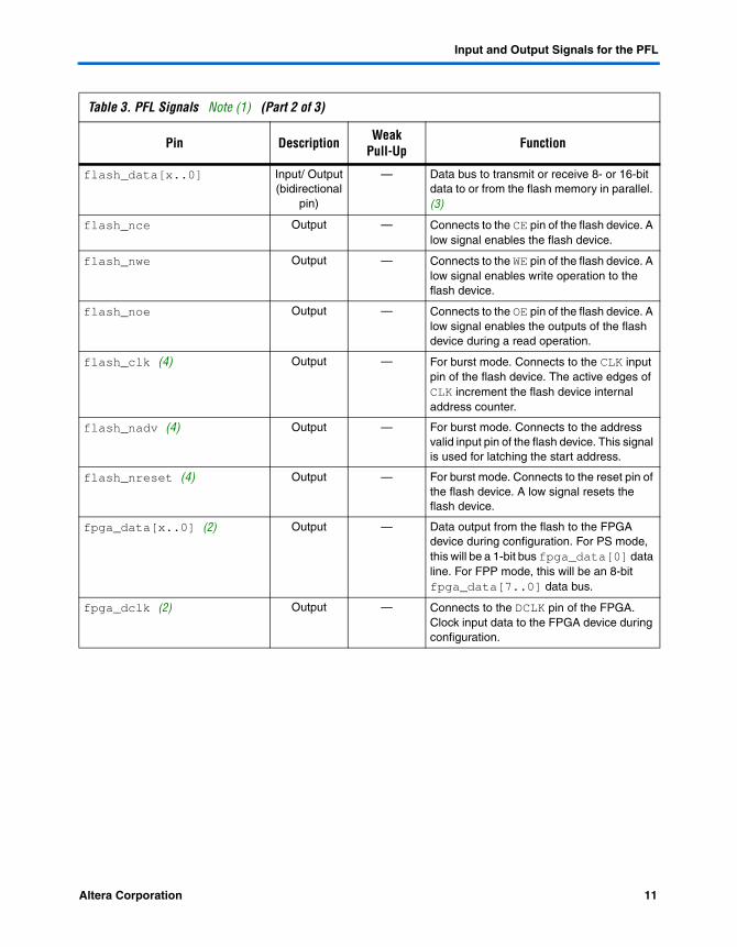
Table 3. PFL Signals Note (1) (Part 1 of 3)
Pin Description WeakPull-Up Function
pfl_nreset Input — Asynchronous reset for the PFL. Pull high to enable the FPGA configuration. Otherwise, to prevent FPGA configuration, pull low at all times when the PFL is not used. This pin does not affect the flash programming.
pfl_flash_access_granted Input — Used for system-level synchronization. This pin can be driven by a processor or any arbitrator that controls access to the flash. This active high pin should be connected permanently high if you want the PFL as the flash master. Pulling it low prevents the JTAG to access the flash and FPGA configuration.
pfl_clk (2) Input — User input clock for the device. Frequency should match the frequency specified in the megafunction and should not be higher than the maximum DCLK frequency specified for the specific FPGA during configuration. (1)
fpga_pgm[2..0] (2) Input — Determines the page to be used for the configuration.
fpga_conf_done (2) Input 10-kΩ Pull-Up Resistor
Connects to the CONF_DONE pin of the FPGA. The FPGA releases the pin high if configuration is successful.
fpga_nstatus (2) Input 10-kΩ Pull-Up Resistor
Connects to the nSTATUS pin of the FPGA. FPGA pulls the pin low if a configuration error occurs.
pfl_nreconfigure (2) Input — Initiates a reconfiguration of the FPGA. This pin can be connected to a switch where you can select a high or low input. A low input initiates a reconfiguration of the FPGA.
pfl_flash_access_request Output — Used for system-level synchronization. This pin can be connected to a processor or arbitrator, if needed. The PFL drives this pin high when JTAG accesses the flash or PFL configures the FPGA. This output pin works in conjunction with the flash_noe and flash_nwe pins.
flash_addr[x..0] Output — Address inputs for memory addresses. The most significant bit (MSB) depends on the density of the flash device as well as the width of the flash_data bus.
10 Altera Corporation
Input and Output Signals for the PFL
flash_data[x..0] Input/ Output(bidirectional
pin)
— Data bus to transmit or receive 8- or 16-bit data to or from the flash memory in parallel. (3)
flash_nce Output — Connects to the CE pin of the flash device. A low signal enables the flash device.
flash_nwe Output — Connects to the WE pin of the flash device. A low signal enables write operation to the flash device.
flash_noe Output — Connects to the OE pin of the flash device. A low signal enables the outputs of the flash device during a read operation.
flash_clk (4) Output — For burst mode. Connects to the CLK input pin of the flash device. The active edges of CLK increment the flash device internal address counter.
flash_nadv (4) Output — For burst mode. Connects to the address valid input pin of the flash device. This signal is used for latching the start address.
flash_nreset (4) Output — For burst mode. Connects to the reset pin of the flash device. A low signal resets the flash device.
fpga_data[x..0] (2) Output — Data output from the flash to the FPGA device during configuration. For PS mode, this will be a 1-bit bus fpga_data[0] data line. For FPP mode, this will be an 8-bit fpga_data[7..0] data bus.
fpga_dclk (2) Output — Connects to the DCLK pin of the FPGA. Clock input data to the FPGA device during configuration.
Table 3. PFL Signals Note (1) (Part 2 of 3)
Pin Description WeakPull-Up Function
Altera Corporation 11
Using the Parallel Flash Loader with the Quartus II Software
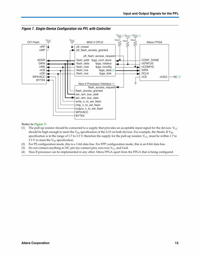
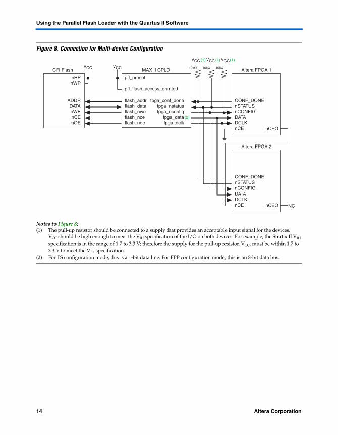
Figure 7 shows the configuration interface connections between the MAX II device, CFI flash memory, an Altera FPGA, and the controller or processor for the PFL solution. In Figure 7, the Nios® II processor represents the controller or processor. The Nios II processor is implemented in the Altera FPGA. The MAX II CPLD and the Nios II processor are able to program the CFI flash individually. The flash_access_granted and flash_access_request pins of the MAX II CPLD and the Nios II processor must be connected together to prevent both processors from accessing the CFI flash at the same time. Figure 8 shows the connection for multi-device configuration.
f For more details about the FPGA configuration, refer to the Configuration Handbook.
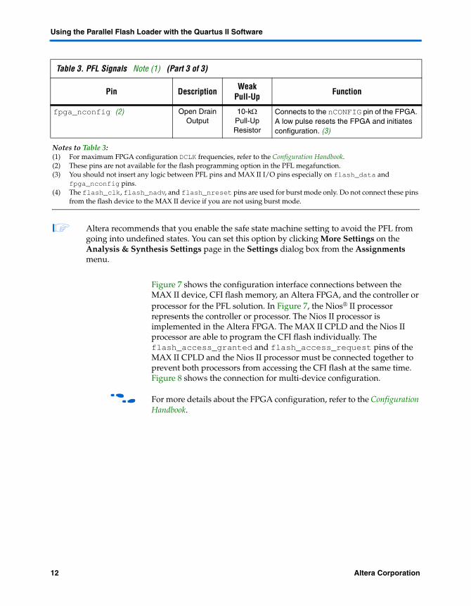
fpga_nconfig (2) Open DrainOutput
10-kΩ Pull-Up Resistor
Connects to the nCONFIG pin of the FPGA. A low pulse resets the FPGA and initiates configuration. (3)
Notes to Table 3: (1) For maximum FPGA configuration DCLK frequencies, refer to the Configuration Handbook.(2) These pins are not available for the flash programming option in the PFL megafunction.(3) You should not insert any logic between PFL pins and MAX II I/O pins especially on flash_data and
fpga_nconfig pins.(4) The flash_clk, flash_nadv, and flash_nreset pins are used for burst mode only. Do not connect these pins
from the flash device to the MAX II device if you are not using burst mode.
1 Altera recommends that you enable the safe state machine setting to avoid the PFL from going into undefined states. You can set this option by clicking More Settings on the Analysis & Synthesis Settings page in the Settings dialog box from the Assignments menu.
Table 3. PFL Signals Note (1) (Part 3 of 3)
Pin Description WeakPull-Up Function
12 Altera Corporation
Input and Output Signals for the PFL
Figure 7. Single-Device Configuration via PFL with Controller
Notes to Figure 7:(1) The pull-up resistor should be connected to a supply that provides an acceptable input signal for the devices. VCC
should be high enough to meet the VIH specification of the I/O on both devices. For example, the Stratix II VIH specification is in the range of 1.7 to 3.3 V; therefore the supply for the pull-up resistor, VCC, must be within 1.7 to 3.3 V to meet the VIH specification.
(2) For PS configuration mode, this is a 1-bit data line. For FPP configuration mode, this is an 8-bit data bus.(3) Do not connect anything to NC pin (no connect pin), not even VCC and Gnd.(4) Nios II processor can be implemented in any other Altera FPGA apart from the FPGA that is being configured.
pfl_nresetpfl_flash_access_granted
flash_addrflash_dataflash_nweflash_nceflash_noe
fpga_conf_donefpga_nstatusfpga_nconfig
fpga_datafpga_dclk
CONF_DONEnSTATUSnCONFIGDATADCLKnCE nCEO
nRPnWP
ADDRDATAnWEnCEnOE
WP#/ACCBYTE#
VCC
10kΩ
VCC
Altera FPGAMAX II CPLDCFI Flash 10kΩ
VCC
10kΩVCC VCC
(1)(1)(1)
(2)
Nios II Processor Interface
(3)
(4)
flash_access_grantedext_ram_bus_addrext_ram_bus_datawrite_n_to_ext_flashchip_n_to_ext_flashoutput_n_to_ext_flashWP#/ACCBYTE#
flash_access_request
pfl_flash_access_request
NC
Altera Corporation 13
Using the Parallel Flash Loader with the Quartus II Software
Figure 8. Connection for Multi-device Configuration
Notes to Figure 8:(1) The pull-up resistor should be connected to a supply that provides an acceptable input signal for the devices.
VCC should be high enough to meet the VIH specification of the I/O on both devices. For example, the Stratix II VIH specification is in the range of 1.7 to 3.3 V; therefore the supply for the pull-up resistor, VCC, must be within 1.7 to 3.3 V to meet the VIH specification.
(2) For PS configuration mode, this is a 1-bit data line. For FPP configuration mode, this is an 8-bit data bus.
pfl_nreset
pfl_flash_access_granted
flash_addrflash_dataflash_nweflash_nceflash_noe
fpga_conf_donefpga_nstatusfpga_nconfig
fpga_datafpga_dclk
CONF_DONEnSTATUSnCONFIGDATADCLKnCE nCEO
nRPnWP
ADDRDATAnWEnCEnOE
VCC
10kΩ
VCC
Altera FPGA 1MAX II CPLDCFI Flash 10kΩ
VCC
10kΩVCC VCC
(1)(1)(1)
(2)
CONF_DONEnSTATUSnCONFIGDATADCLKnCE nCEO NC
Altera FPGA 2
14 Altera Corporation
PFL Design Example
PFL Design Example
The PFL megafunction is able to support flash programming and multiple FPGA configurations, and at the same time allow another processor to access the flash device. This approach is useful if you need an alternative way to program the flash device other than through the PFL megafunction, or if you need to allow another processor to access the flash device. For example, you can use the PFL megafunction to program the flash and configure the FPGA with a Nios II processor. The Nios II processor that is configured utilizes the non-configuration data stored in the same flash device.
This design example shows you how to program a flash device in a system with multiple processors. You can use the processor and the PFL megafunction to program a flash device. The processor used in this example is a Nios II processor. (You can use other processors or microcontrollers in place of the Nios II processor.) The Nios II processor is a general-purpose RISC processor core that is implemented in Altera FPGAs. A Nios II processor system is equivalent to a microcontroller or “computer-on-a-chip”, which includes a CPU and a combination of peripherals and memory on a single chip. The Nios II flash programmer is part of the Nios II development tools, and is a convenient method for programming flash devices.
The rest of this section explains the implementation of flash programming interface between the PFL megafunction in the MAX II device and a Nios II processor in an Altera FPGA.
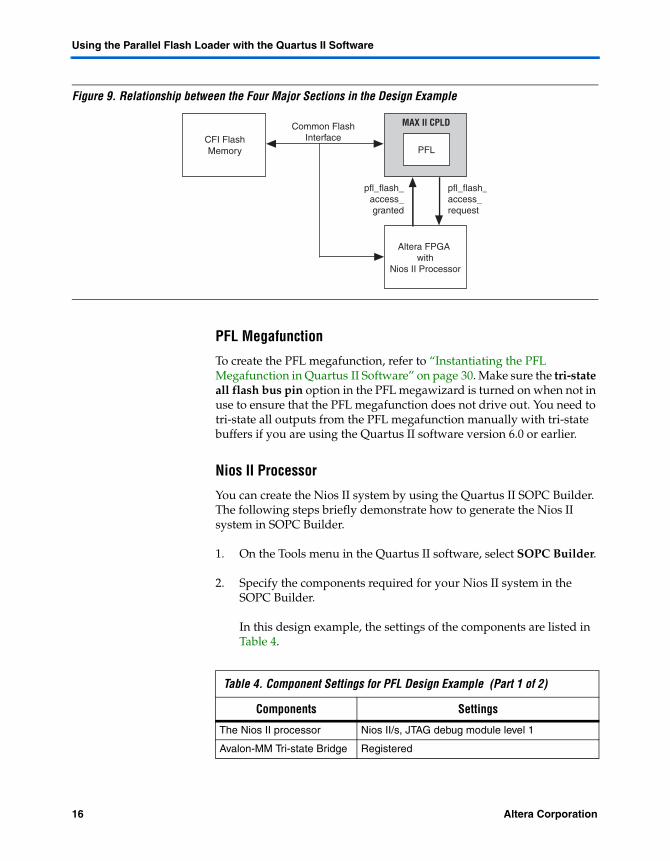
This design example consists of four major sections—the PFL megafunction, the Nios II processor, the flash device, and the pfl_flash_access_request and pfl_flash_access_granted pins. Refer to Figure 9 for the relationship between the four sections. The PFL megafunction and the Nios II processor are created separately with the Quartus II software. You can create either the PFL megafunction or the Nios II system first, as explained in the following sub-sections.
Altera Corporation 15
Using the Parallel Flash Loader with the Quartus II Software
Figure 9. Relationship between the Four Major Sections in the Design Example
PFL Megafunction
To create the PFL megafunction, refer to “Instantiating the PFL Megafunction in Quartus II Software” on page 30. Make sure the tri-state all flash bus pin option in the PFL megawizard is turned on when not in use to ensure that the PFL megafunction does not drive out. You need to tri-state all outputs from the PFL megafunction manually with tri-state buffers if you are using the Quartus II software version 6.0 or earlier.
Nios II Processor
You can create the Nios II system by using the Quartus II SOPC Builder. The following steps briefly demonstrate how to generate the Nios II system in SOPC Builder.
1. On the Tools menu in the Quartus II software, select SOPC Builder.
2. Specify the components required for your Nios II system in the SOPC Builder.
In this design example, the settings of the components are listed in Table 4.
MAX II CPLD
CFI FlashMemory
Altera FPGA with
Nios II Processor
Common FlashInterface
PFL
pfl_flash_access_granted
pfl_flash_access_request
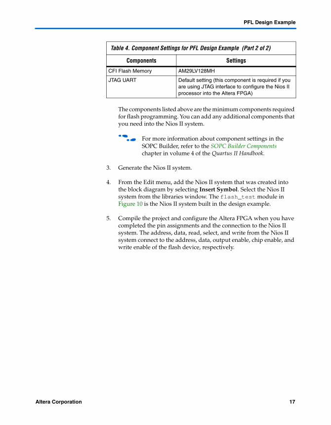
Table 4. Component Settings for PFL Design Example (Part 1 of 2)
Components Settings
The Nios II processor Nios II/s, JTAG debug module level 1
Avalon-MM Tri-state Bridge Registered
16 Altera Corporation
PFL Design Example
The components listed above are the minimum components required for flash programming. You can add any additional components that you need into the Nios II system.
f For more information about component settings in the SOPC Builder, refer to the SOPC Builder Components chapter in volume 4 of the Quartus II Handbook.
3. Generate the Nios II system.
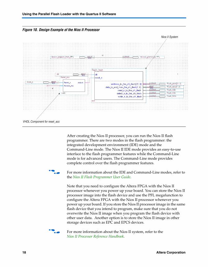
4. From the Edit menu, add the Nios II system that was created into the block diagram by selecting Insert Symbol. Select the Nios II system from the libraries window. The flash_test module in Figure 10 is the Nios II system built in the design example.
5. Compile the project and configure the Altera FPGA when you have completed the pin assignments and the connection to the Nios II system. The address, data, read, select, and write from the Nios II system connect to the address, data, output enable, chip enable, and write enable of the flash device, respectively.
CFI Flash Memory AM29LV128MH
JTAG UART Default setting (this component is required if you are using JTAG interface to configure the Nios II processor into the Altera FPGA)
Table 4. Component Settings for PFL Design Example (Part 2 of 2)
Components Settings
Altera Corporation 17
Using the Parallel Flash Loader with the Quartus II Software
Figure 10. Design Example of the Nios II Processor
After creating the Nios II processor, you can run the Nios II flash programmer. There are two modes in the flash programmer: the integrated development environment (IDE) mode and the Command-Line mode. The Nios II IDE mode provides an easy-to-use interface to the flash programmer features while the Command-Line mode is for advanced users. The Command-Line mode provides complete control over the flash programmer features.
f For more information about the IDE and Command-Line modes, refer to the Nios II Flash Programmer User Guide.
Note that you need to configure the Altera FPGA with the Nios II processor whenever you power up your board. You can store the Nios II processor image into the flash device and use the PFL megafunction to configure the Altera FPGA with the Nios II processor whenever you power up your board. If you store the Nios II processor image in the same flash device that you intend to program, make sure that you do not overwrite the Nios II image when you program the flash device with other user data. Another option is to store the Nios II image in other storage devices such as EPC and EPCS devices.
f For more information about the Nios II system, refer to the Nios II Processor Reference Handbook.
Nios II System
VHDL Component for reset_acc
18 Altera Corporation
PFL Design Example
Flash Device
For the flash device, take note of the byte enable pin. Pulling this pin low places the flash device in ×8 data width mode. A high input to this pin places the flash device in ×16 data width mode. The PFL megafunction and the Nios II processor data pin must be assigned according to the data width mode you have selected.
The read or write access time depends on the flash device type. In the PFL megafunction, the write access time is encoded into the PFL megafunction. You do not need to specify the write access time but you would need to specify the read access time in the PFL megawizard. As for the Nios II system, you need to specify the read or write access time if you select the custom flash option. Refer to the flash device datasheet for the read or write access time. Note that the PFL megafunction and the Nios II system are not able to perform a selective read during a write operation as the data bus only allows single directional data. It does not support bidirectional flow of data concurrently.
pfl_flash_access_request and pfl_flash_access_granted Pins
As mentioned earlier, the Nios II processor and the PFL megafunction share the same bus line to the flash device. However, they must not access or program the flash device at the same time as this causes data contention. To ensure that only one processor is accessing the flash device, you must tri-state all output pins that connect to the flash device of one processor while the other processor is accessing the flash device. To achieve this, utilize the pfl_flash_access_request and pfl_flash_access_granted pins in the PFL megafunction. From Table 3 on PFL signal, the PFL megafunction drives the pfl_flash_access_request pin high whenever it requires access to the flash device, and the PFL megafunction connects to the flash device whenever it receives a high input signal at pfl_flash_access_granted pin. Refer to Table 5 on how to utilize the access request and access granted pins to ensure that both processors are not accessing the flash device at the same time.
Altera Corporation 19
Using the Parallel Flash Loader with the Quartus II Software
In this design example, the Nios II processor utilizes a VHDL code component, reset_acc, which is created to pull the reset_n of the Nios II processor low whenever pfl_flash_access_request pin goes high. When reset_n goes low, the Nios II processor is disabled and all output pins from the Nios II processor are tri-stated.
As for the pfl_flash_access_request pin and the pfl_flash_access_granted pin, create an input and output pin to route the pfl_flash_access_request signal to pfl_flash_access_granted pin in the block diagram of the Nios II system. The PFL megafunction starts accessing the flash device when it receives a high input signal on the pfl_flash_access_granted pin. Refer to Figure 10 on page 2–18 for the connection of the reset_acc component to the Nios II processor and the connection of the pfl_flash_access_request and the pfl_flash_access_granted pins. The VHDL code for reset_acc is attached in the design example.
For the PFL megafunction, the tri-state all flash bus pin when not in use option disables the PFL megafunction whenever pfl_flash_access_granted pin receives a low input. This option is only available in the Quartus II software version 6.1 and later. You need to tri-state all outputs from the PFL megafunction manually with tri-state buffers if you are using Quartus II software version 6.0 or earlier.
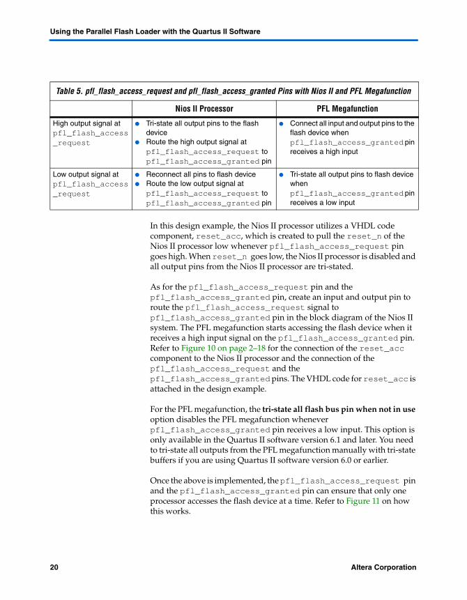
Once the above is implemented, the pfl_flash_access_request pin and the pfl_flash_access_granted pin can ensure that only one processor accesses the flash device at a time. Refer to Figure 11 on how this works.
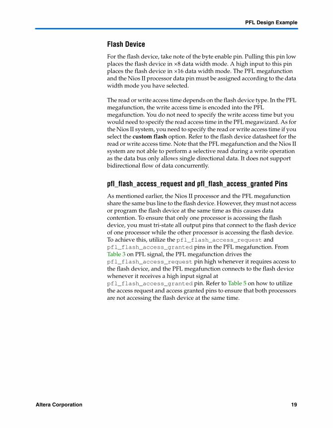
Table 5. pfl_flash_access_request and pfl_flash_access_granted Pins with Nios II and PFL Megafunction
Nios II Processor PFL Megafunction
High output signal at pfl_flash_access_request
● Tri-state all output pins to the flash device
● Route the high output signal at pfl_flash_access_request to pfl_flash_access_granted pin
● Connect all input and output pins to the flash device when pfl_flash_access_granted pin receives a high input
Low output signal at pfl_flash_access_request
● Reconnect all pins to flash device● Route the low output signal at
pfl_flash_access_request to pfl_flash_access_granted pin
● Tri-state all output pins to flash device when pfl_flash_access_granted pin receives a low input
20 Altera Corporation
PFL Design Example
Figure 11. Nios II Processor and the PFL Megafunction Accessing the Flash Device
Using a Processor or Controller in place of the Nios II System
To implement the above using other processors or controllers, make sure that the access granted and access request pins of the PFL are connected to your processor with the same concept mentioned in “pfl_flash_access_request and pfl_flash_access_granted Pins” on page 19.
You need to specify the flash device read or write access time in your processor or controller as well. Make sure that the output pins from your processor are tri-stated when access request is high to avoid data contention when the PFL megafunction is accessing the flash device.
Nios II processor connectsto the flash device
PFL megafunction pulls the pfl_flash_access_request pin highto request access to the flash device.
PFL megafunction requestsfor access to flash device
Nios II processor receives the PFL megafunction
PFL megafunction accessesthe flash device
PFL megafunction releasesthe flash device
By default, Nios II processor is connected to the flash device. All PFL megafunction output pins are tri-stated.
Nios II processor tri-states all output pins to flash device and routesthe output of pfl_flash_access_request to pfl_flash_access _granted.
PFL megafunction accesses the flash device when it receivesa high input at pfl_flash_access_granted input pin.pfl_flash_access_request pin stays high as long asPFL is connected to the flash device.
The PFL megafunction pulls the pfl_flash_access_request output pin lowwhen it accesses the flash device.
Altera Corporation 21
Using the Parallel Flash Loader with the Quartus II Software
PFL and Flash Address Mapping
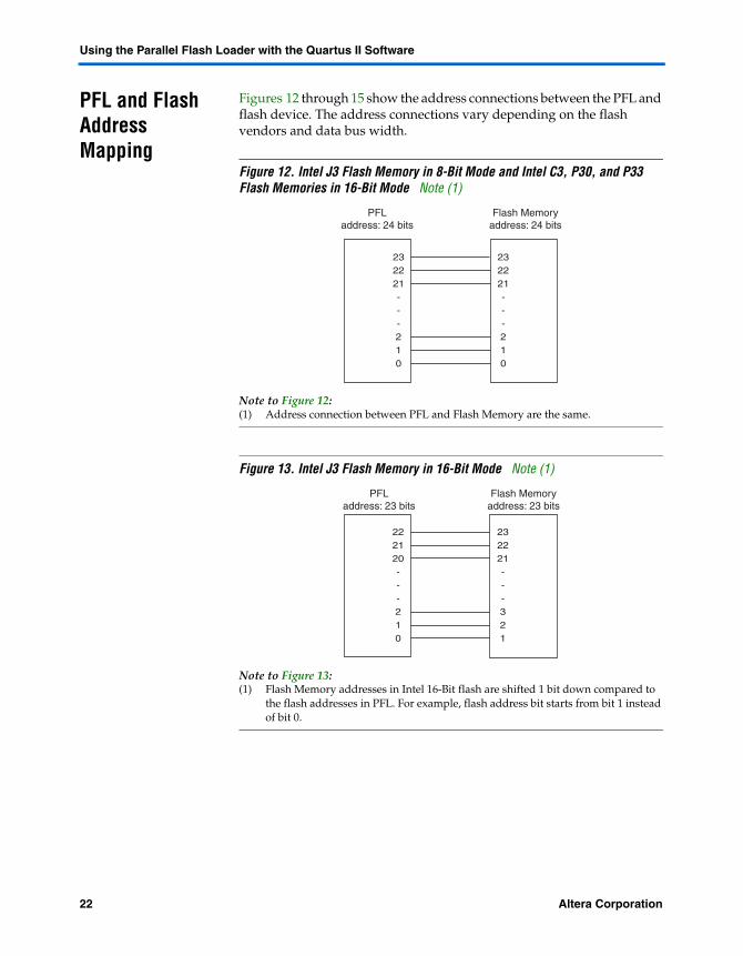
Figures 12 through 15 show the address connections between the PFL and flash device. The address connections vary depending on the flash vendors and data bus width.
Figure 12. Intel J3 Flash Memory in 8-Bit Mode and Intel C3, P30, and P33 Flash Memories in 16-Bit Mode Note (1)
Note to Figure 12:(1) Address connection between PFL and Flash Memory are the same.
Figure 13. Intel J3 Flash Memory in 16-Bit Mode Note (1)
Note to Figure 13:(1) Flash Memory addresses in Intel 16-Bit flash are shifted 1 bit down compared to
the flash addresses in PFL. For example, flash address bit starts from bit 1 instead of bit 0.
232221---210
PFLaddress: 24 bits
232221---210
Flash Memoryaddress: 24 bits
222120---210
PFLaddress: 23 bits
232221---321
Flash Memoryaddress: 23 bits
22 Altera Corporation
PFL and Flash Address Mapping
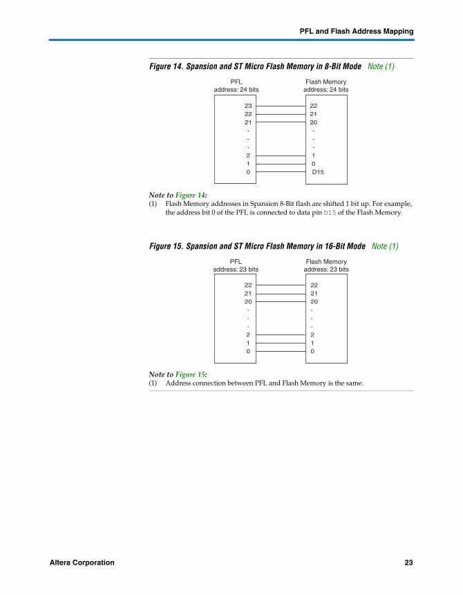
Figure 14. Spansion and ST Micro Flash Memory in 8-Bit Mode Note (1)
Note to Figure 14:(1) Flash Memory addresses in Spansion 8-Bit flash are shifted 1 bit up. For example,
the address bit 0 of the PFL is connected to data pin D15 of the Flash Memory.
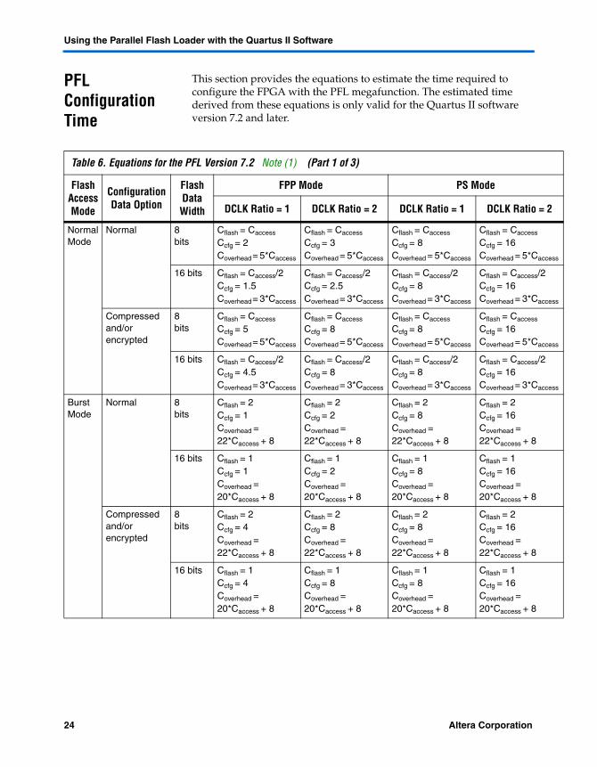
Figure 15. Spansion and ST Micro Flash Memory in 16-Bit Mode Note (1)
Note to Figure 15:(1) Address connection between PFL and Flash Memory is the same.
232221---210
PFLaddress: 24 bits
222120---10
D15
Flash Memoryaddress: 24 bits
222120---210
PFLaddress: 23 bits
222120---210
Flash Memoryaddress: 23 bits
Altera Corporation 23
Using the Parallel Flash Loader with the Quartus II Software
2
cess
cess
cess
cess
PFL Configuration Time
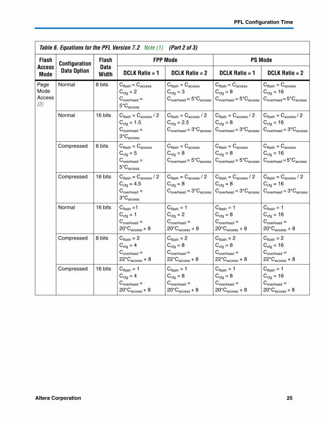
This section provides the equations to estimate the time required to configure the FPGA with the PFL megafunction. The estimated time derived from these equations is only valid for the Quartus II software version 7.2 and later.
Table 6. Equations for the PFL Version 7.2 Note (1) (Part 1 of 3)
Flash Access Mode
Configuration Data Option
Flash Data Width
FPP Mode PS Mode
DCLK Ratio = 1 DCLK Ratio = 2 DCLK Ratio = 1 DCLK Ratio =
Normal Mode
Normal 8bits
Cflash = Caccess
Ccfg = 2Coverhead = 5*Caccess
Cflash = Caccess
Ccfg = 3Coverhead = 5*Caccess
Cflash = Caccess
Ccfg = 8Coverhead = 5*Caccess
Cflash = Caccess
Ccfg = 16Coverhead = 5*Cac
16 bits Cflash = Caccess/2Ccfg = 1.5Coverhead = 3*Caccess
Cflash = Caccess/2Ccfg = 2.5Coverhead = 3*Caccess
Cflash = Caccess/2Ccfg = 8Coverhead = 3*Caccess
Cflash = Caccess/2Ccfg = 16Coverhead = 3*Cac
Compressed and/or encrypted
8bits
Cflash = Caccess
Ccfg = 5Coverhead = 5*Caccess
Cflash = Caccess
Ccfg = 8Coverhead = 5*Caccess
Cflash = Caccess
Ccfg = 8Coverhead = 5*Caccess
Cflash = Caccess
Ccfg = 16Coverhead = 5*Cac
16 bits Cflash = Caccess/2Ccfg = 4.5Coverhead = 3*Caccess
Cflash = Caccess/2Ccfg = 8Coverhead = 3*Caccess
Cflash = Caccess/2Ccfg = 8Coverhead = 3*Caccess
Cflash = Caccess/2Ccfg = 16Coverhead = 3*Cac
Burst Mode
Normal 8bits
Cflash = 2Ccfg = 1Coverhead = 22*Caccess + 8
Cflash = 2Ccfg = 2Coverhead = 22*Caccess + 8
Cflash = 2Ccfg = 8Coverhead = 22*Caccess + 8
Cflash = 2Ccfg = 16Coverhead = 22*Caccess + 8
16 bits Cflash = 1Ccfg = 1Coverhead = 20*Caccess + 8
Cflash = 1Ccfg = 2Coverhead = 20*Caccess + 8
Cflash = 1Ccfg = 8Coverhead = 20*Caccess + 8
Cflash = 1Ccfg = 16Coverhead = 20*Caccess + 8
Compressed and/or encrypted
8bits
Cflash = 2Ccfg = 4Coverhead = 22*Caccess + 8
Cflash = 2Ccfg = 8Coverhead = 22*Caccess + 8
Cflash = 2Ccfg = 8Coverhead = 22*Caccess + 8
Cflash = 2Ccfg = 16Coverhead = 22*Caccess + 8
16 bits Cflash = 1Ccfg = 4Coverhead = 20*Caccess + 8
Cflash = 1Ccfg = 8Coverhead = 20*Caccess + 8
Cflash = 1Ccfg = 8Coverhead = 20*Caccess + 8
Cflash = 1Ccfg = 16Coverhead = 20*Caccess + 8
24 Altera Corporation
PFL Configuration Time
cess
2
cess
cess
2
cess
2
Page Mode Access (2)
Normal 8 bits Cflash = Caccess Ccfg = 2Coverhead = 5*Caccess
Cflash = Caccess
Ccfg = 3Coverhead = 5*Caccess
Cflash = Caccess
Ccfg = 8Coverhead = 5*Caccess
Cflash = Caccess
Ccfg = 16Coverhead = 5*Cac
Normal 16 bits Cflash = Caccess / 2 Ccfg = 1.5Coverhead = 3*Caccess
Cflash = Caccess / 2 Ccfg = 2.5Coverhead = 3*Caccess
Cflash = Caccess / 2 Ccfg = 8Coverhead = 3*Caccess
Cflash = Caccess / Ccfg = 16Coverhead = 3*Cac
Compressed 8 bits Cflash = Caccess
Ccfg = 5Coverhead = 5*Caccess
Cflash = Caccess Ccfg = 8Coverhead = 5*Caccess
Cflash = Caccess Ccfg = 8Coverhead = 5*Caccess
Cflash = Caccess Ccfg = 16Coverhead = 5*Cac
Compressed 16 bits Cflash = Caccess / 2 Ccfg = 4.5Coverhead = 3*Caccess
Cflash = Caccess / 2 Ccfg = 8Coverhead = 3*Caccess
Cflash = Caccess / 2 Ccfg = 8Coverhead = 3*Caccess
Cflash = Caccess / Ccfg = 16Coverhead = 3*Cac
Normal 16 bits Cflash =1Ccfg = 1Coverhead = 20*Caccess + 8
Cflash = 1Ccfg = 2Coverhead = 20*Caccess + 8
Cflash = 1Ccfg = 8Coverhead = 20*Caccess + 8
Cflash = 1Ccfg = 16Coverhead = 20*Caccess + 8
Compressed 8 bits Cflash = 2 Ccfg = 4Coverhead = 22*Caccess + 8
Cflash = 2 Ccfg = 8Coverhead = 22*Caccess + 8
Cflash = 2 Ccfg = 8Coverhead = 22*Caccess + 8
Cflash = 2 Ccfg = 16Coverhead = 22*Caccess + 8
Compressed 16 bits Cflash = 1Ccfg = 4Coverhead = 20*Caccess + 8
Cflash = 1 Ccfg = 8Coverhead = 20*Caccess + 8
Cflash = 1 Ccfg = 8Coverhead = 20*Caccess + 8
Cflash = 1 Ccfg = 16Coverhead = 20*Caccess + 8
Table 6. Equations for the PFL Version 7.2 Note (1) (Part 2 of 3)
Flash Access Mode
Configuration Data Option
Flash Data Width
FPP Mode PS Mode
DCLK Ratio = 1 DCLK Ratio = 2 DCLK Ratio = 1 DCLK Ratio =
Altera Corporation 25
Using the Parallel Flash Loader with the Quartus II Software
ing ata
.
2
Here is an example for calculating the configuration time using the following values:
.rbf file size = 577 KB = 590,848 BytesConfiguration Mode: PS without data compression or encryptionFlash access mode: Normal modeFlash data bus width: 16 bitsFlash access time: 100 nsPFL input clock = 10 MHzDCLK ration = 2
The following formulas are used in this calculation:
Caccess = Taccess * Fclk + 1Cflash = Caccess
Ccfg = 16Coverhead = 3 * Cflash
Total clock cycles = Coverhead + max(Cflash,Ccfg) * N
Caccess = Taccess * Fclk + 1
Total clock cycles (from nRESET asserted high to N bytes of data clocked out)= Coverhead + max(Cflash, Ccfg) * N
Note to Table 6:(1) Cflash represents the number of clock cycles required to read from flash.
Ccfg represents the number of input clock cycles to clock out the data (producing between 1 and 16 DCLK cycles, dependon the choice of flash data bus width and FPP/PS mode). The process of reading from the flash and clocking out the dfor configuration are performed in parallel, so only the larger number between Cflash and Ccfg is important. Fclk represents the input clock frequency to the PFL.Taccess time represents the flash access time.Caccess represents the number of clock cycles needed before the data from the flash is ready.N represents the number of bytes to be clocked out. This value can be obtained from the .rbf file for the specific FPGA
(2) Spansion Page Mode support is only available in Quartus II software version 8.0 and later
Table 6. Equations for the PFL Version 7.2 Note (1) (Part 3 of 3)
Flash Access Mode
Configuration Data Option
Flash Data Width
FPP Mode PS Mode
DCLK Ratio = 1 DCLK Ratio = 2 DCLK Ratio = 1 DCLK Ratio =
26 Altera Corporation
Using the PFL in Quartus II Software
By substituting the values into the formulas, you get:
Caccess = 100 ns * 10 MHz + 1 = 2Cflash = 2Ccfg = 16Coverhead = 3 * 2= 6Total clock cycles = 6 + 16 * 590848 = 9453574
At 10 MHz, total configuration time = 9453574/10 MHz = 945 ms.
Using the PFL in Quartus II Software
This section describes the steps for using the PFL feature with the Quartus II software. The process includes:
1. The instantiation of the PFL megafunction in the user design.
2. Converting the SOF(s) that contains the configuration data for the Altera FPGA to a POF specifically for the flash device.
3. Programming the POF into the flash device through the MAX II device using the Quartus II Programmer.
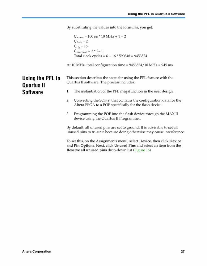
By default, all unused pins are set to ground. It is advisable to set all unused pins to tri-state because doing otherwise may cause interference.
To set this, on the Assignments menu, select Device, then click Device and Pin Options. Next, click Unused Pins and select an item from the Reserve all unused pins drop-down list (Figure 16).
Altera Corporation 27
Using the Parallel Flash Loader with the Quartus II Software
Figure 16. Reserve All Unused Pins
28 Altera Corporation
Using the PFL in Quartus II Software
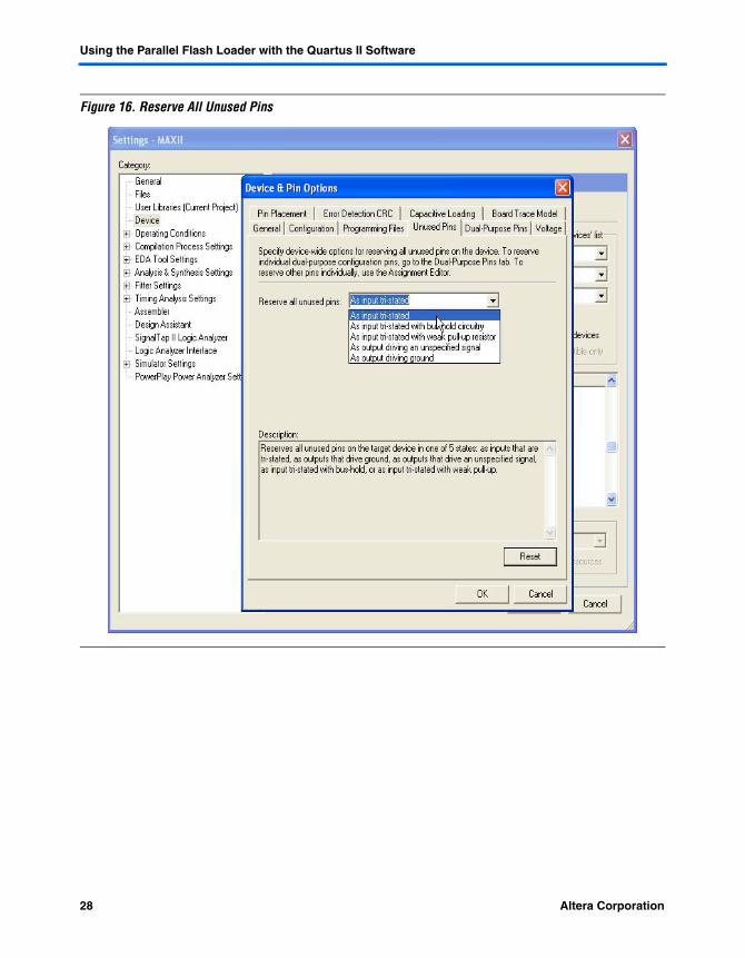
Figure 17 shows the steps for using the PFL. The Quartus II software does not support simulation of the JTAG pins or the programming process of the MAX II or flash device. However, simulation is possible for FPGA configuration but with the condition that there are proper flash vectors and FPGA responses. Examples of the flash vectors are flash_addr and flash_data; examples of the FPGA responses are fpga_conf_done and fpga_nstatus.
Figure 17. Quartus II Software PFL Steps
Create a new MAX II Project, instantiate the PFL Megafunction in
the MAX II Design, and make Pin Assignments
Add MAX II POF toQuartus II Programmer
Add Flash POF in the Quartus II Programmer
Program the MAX II and Flash Devices
MAX II configures the FPGA withConfiguration Data from the Flash Device
Compile andobtain FPGA SOF(s)
Convert to POF forTargeted
Flash
Compile& ObtainMAX IIPOF
Add SOF(s) for conversion to POF
Create new FPGAproject(s)
Create the optional Jam programming file
Altera Corporation 29
Using the Parallel Flash Loader with the Quartus II Software
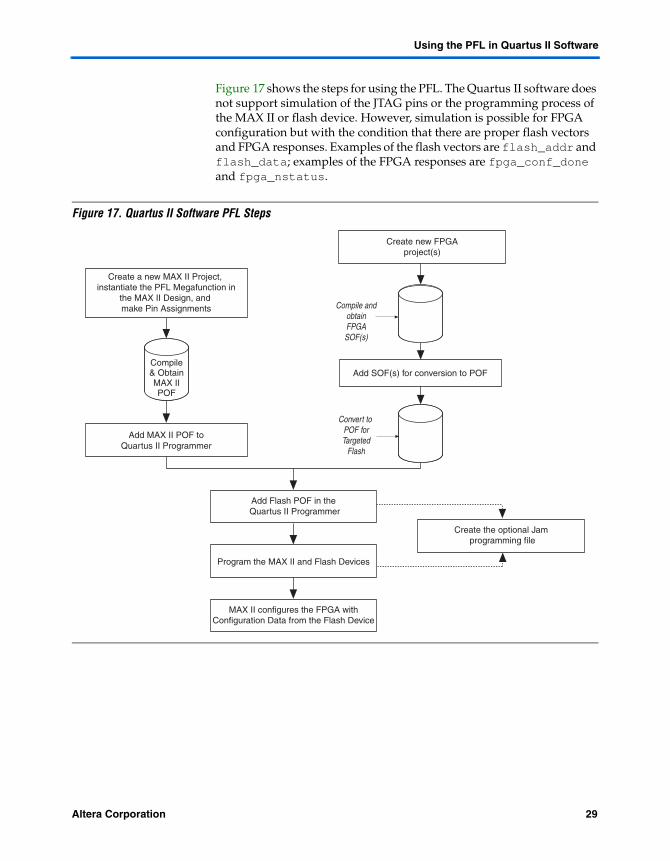
Instantiating the PFL Megafunction in Quartus II Software
Perform the following steps to generate a PFL megafunction instantiation. You should then instantiate the megafunction in your MAX II top-level design.
1. On the Tools menu, select MegaWizard Plug-In Manager.
2. Select Create a new custom megafunction variation and click Next.
3. Select the MAX II device family.
4. Select Parallel Flash Loader from the megafunction list.
5. Select the Hardware Description Language (HDL) output file type. Click Next (Verilog HDL was chosen for this example).
6. Specify the directory and output filename. The dialog box should now be similar to Figure 18. Click Next.
Figure 18. Selecting the PFL Megafunction
30 Altera Corporation
Using the PFL in Quartus II Software
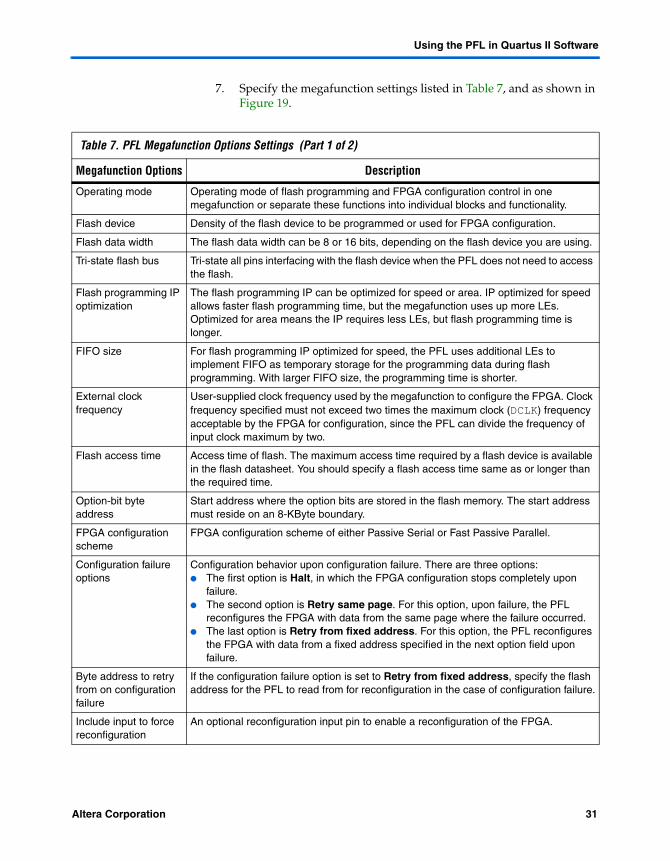
7. Specify the megafunction settings listed in Table 7, and as shown in Figure 19.
Table 7. PFL Megafunction Options Settings (Part 1 of 2)
Megafunction Options Description
Operating mode Operating mode of flash programming and FPGA configuration control in one megafunction or separate these functions into individual blocks and functionality.
Flash device Density of the flash device to be programmed or used for FPGA configuration.
Flash data width The flash data width can be 8 or 16 bits, depending on the flash device you are using.
Tri-state flash bus Tri-state all pins interfacing with the flash device when the PFL does not need to access the flash.
Flash programming IP optimization
The flash programming IP can be optimized for speed or area. IP optimized for speed allows faster flash programming time, but the megafunction uses up more LEs. Optimized for area means the IP requires less LEs, but flash programming time is longer.
FIFO size For flash programming IP optimized for speed, the PFL uses additional LEs to implement FIFO as temporary storage for the programming data during flash programming. With larger FIFO size, the programming time is shorter.
External clock frequency
User-supplied clock frequency used by the megafunction to configure the FPGA. Clock frequency specified must not exceed two times the maximum clock (DCLK) frequency acceptable by the FPGA for configuration, since the PFL can divide the frequency of input clock maximum by two.
Flash access time Access time of flash. The maximum access time required by a flash device is available in the flash datasheet. You should specify a flash access time same as or longer than the required time.
Option-bit byte address
Start address where the option bits are stored in the flash memory. The start address must reside on an 8-KByte boundary.
FPGA configuration scheme
FPGA configuration scheme of either Passive Serial or Fast Passive Parallel.
Configuration failure options
Configuration behavior upon configuration failure. There are three options:● The first option is Halt, in which the FPGA configuration stops completely upon
failure.● The second option is Retry same page. For this option, upon failure, the PFL
reconfigures the FPGA with data from the same page where the failure occurred.● The last option is Retry from fixed address. For this option, the PFL reconfigures
the FPGA with data from a fixed address specified in the next option field upon failure.
Byte address to retry from on configuration failure
If the configuration failure option is set to Retry from fixed address, specify the flash address for the PFL to read from for reconfiguration in the case of configuration failure.
Include input to force reconfiguration
An optional reconfiguration input pin to enable a reconfiguration of the FPGA.
Altera Corporation 31
Using the Parallel Flash Loader with the Quartus II Software
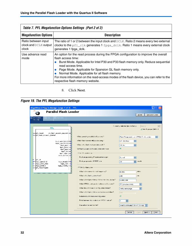
8. Click Next.
Figure 19. The PFL Megafunction Settings
Ratio between input clock and DCLK output clock
The ratio of 1 or 2 between the input clock and DCLK. Ratio 2 means every two external clocks to the pfl_clk generates 1 fpga_dclk. Ratio 1 means every external clock generates 1 fpga_dclk.
Use advance read mode
An option for the read process during the FPGA configuration to improve the overall flash access time:● Burst Mode. Applicable for Intel P30 and P33 flash memory only. Reduce sequential
read access time. ● Page Mode. Applicable for Spansion GL flash memory only.● Normal Mode. Applicable for all flash memory.For more information on the read-access modes of the flash device, you can refer to the respective flash memory website.
Table 7. PFL Megafunction Options Settings (Part 2 of 2)
Megafunction Options Description
32 Altera Corporation
Using the PFL in Quartus II Software
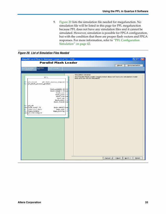
9. Figure 20 lists the simulation file needed for megafunction. No simulation file will be listed in this page for PFL megafunction because PFL does not have any simulation files and it cannot be simulated. However, simulation is possible for FPGA configuration, but with the condition that there are proper flash vectors and FPGA responses. For more information, refer to “PFL Configuration Simulation” on page 42.
Figure 20. List of Simulation Files Needed
Altera Corporation 33
Using the Parallel Flash Loader with the Quartus II Software
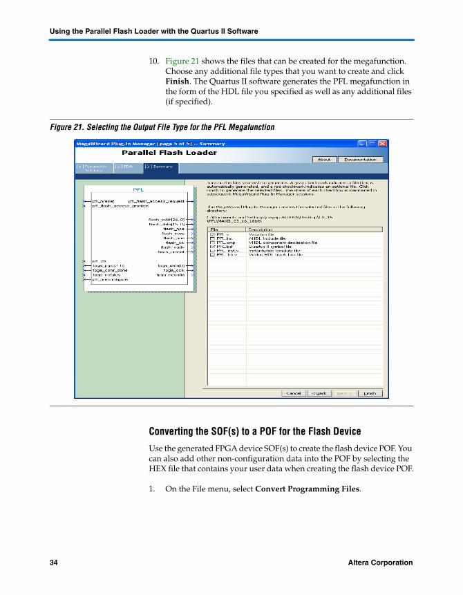
10. Figure 21 shows the files that can be created for the megafunction. Choose any additional file types that you want to create and click Finish. The Quartus II software generates the PFL megafunction in the form of the HDL file you specified as well as any additional files (if specified).
Figure 21. Selecting the Output File Type for the PFL Megafunction
Converting the SOF(s) to a POF for the Flash Device
Use the generated FPGA device SOF(s) to create the flash device POF. You can also add other non-configuration data into the POF by selecting the HEX file that contains your user data when creating the flash device POF.
1. On the File menu, select Convert Programming Files.
34 Altera Corporation
Using the PFL in Quartus II Software
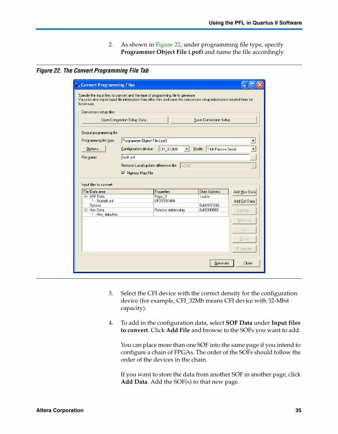
2. As shown in Figure 22, under programming file type, specify Programmer Object File (.pof) and name the file accordingly.
Figure 22. The Convert Programming File Tab
3. Select the CFI device with the correct density for the configuration device (for example, CFI_32Mb means CFI device with 32-Mbit capacity).
4. To add in the configuration data, select SOF Data under Input files to convert. Click Add File and browse to the SOFs you want to add.
You can place more than one SOF into the same page if you intend to configure a chain of FPGAs. The order of the SOFs should follow the order of the devices in the chain.
If you want to store the data from another SOF in another page, click Add Data. Add the SOF(s) to that new page.
Altera Corporation 35
Using the Parallel Flash Loader with the Quartus II Software
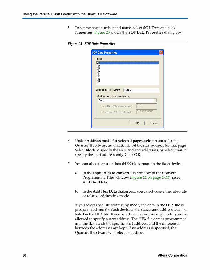
5. To set the page number and name, select SOF Data and click Properties. Figure 23 shows the SOF Data Properties dialog box.
Figure 23. SOF Data Properties
6. Under Address mode for selected pages, select Auto to let the Quartus II software automatically set the start address for that page. Select Block to specify the start and end addresses, or select Start to specify the start address only. Click OK.
7. You can also store user data (HEX file format) in the flash device:
a. In the Input files to convert sub-window of the Convert Programming Files window (Figure 22 on page 2–35), select Add Hex Data.
b. In the Add Hex Data dialog box, you can choose either absolute or relative addressing mode.
If you select absolute addressing mode, the data in the HEX file is programmed into the flash device at the exact same address location listed in the HEX file. If you select relative addressing mode, you are allowed to specify a start address. The HEX file data is programmed into the flash with the specific start address, and the differences between the addresses are kept. If no address is specified, the Quartus II software will select an address.
36 Altera Corporation
Using the PFL in Quartus II Software
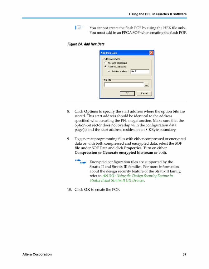
1 You cannot create the flash POF by using the HEX file only. You must add in an FPGA SOF when creating the flash POF.
Figure 24. Add Hex Data
8. Click Options to specify the start address where the option bits are stored. This start address should be identical to the address specified when creating the PFL megafunction. Make sure that the option-bit sector does not overlap with the configuration data page(s) and the start address resides on an 8-KByte boundary.
9. To generate programming files with either compressed or encrypted data or with both compressed and encrypted data, select the SOF file under SOF Data and click Properties. Turn on either Compression or Generate encrypted bitstream or both.
f Encrypted configuration files are supported by the Stratix II and Stratix III families. For more information about the design security feature of the Stratix II family, refer to AN 341: Using the Design Security Feature in Stratix II and Stratix II GX Devices.
10. Click OK to create the POF.
Altera Corporation 37
Using the Parallel Flash Loader with the Quartus II Software
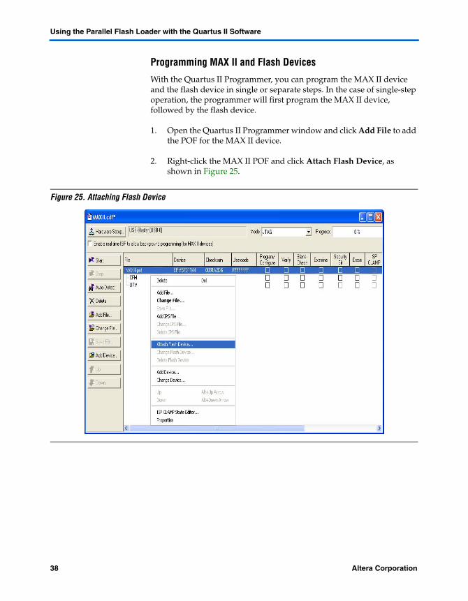
Programming MAX II and Flash Devices
With the Quartus II Programmer, you can program the MAX II device and the flash device in single or separate steps. In the case of single-step operation, the programmer will first program the MAX II device, followed by the flash device.
1. Open the Quartus II Programmer window and click Add File to add the POF for the MAX II device.
2. Right-click the MAX II POF and click Attach Flash Device, as shown in Figure 25.
Figure 25. Attaching Flash Device
38 Altera Corporation
Using the PFL in Quartus II Software
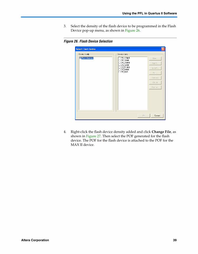
3. Select the density of the flash device to be programmed in the Flash Device pop-up menu, as shown in Figure 26.
Figure 26. Flash Device Selection
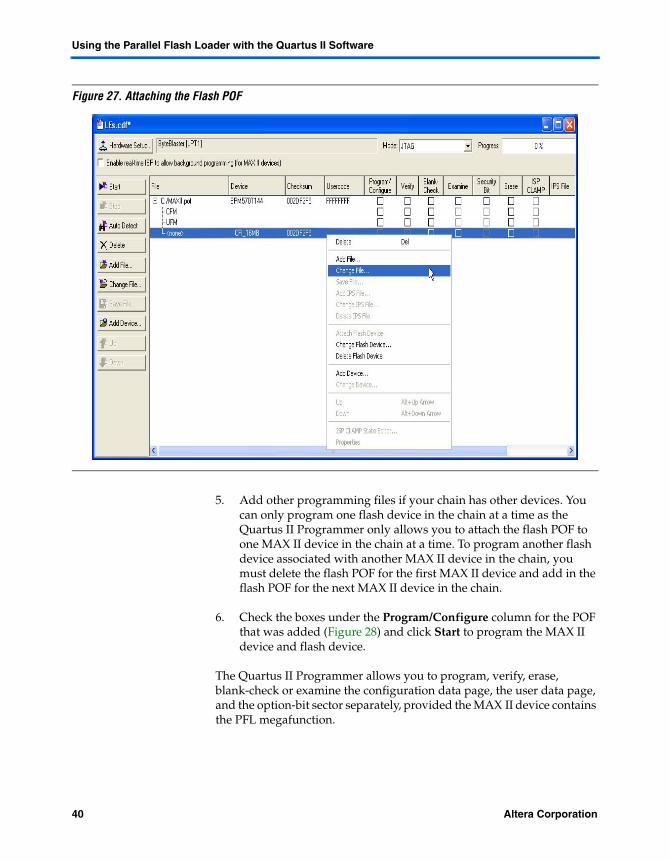
4. Right-click the flash device density added and click Change File, as shown in Figure 27. Then select the POF generated for the flash device. The POF for the flash device is attached to the POF for the MAX II device.
Altera Corporation 39
Using the Parallel Flash Loader with the Quartus II Software
Figure 27. Attaching the Flash POF
5. Add other programming files if your chain has other devices. You can only program one flash device in the chain at a time as the Quartus II Programmer only allows you to attach the flash POF to one MAX II device in the chain at a time. To program another flash device associated with another MAX II device in the chain, you must delete the flash POF for the first MAX II device and add in the flash POF for the next MAX II device in the chain.
6. Check the boxes under the Program/Configure column for the POF that was added (Figure 28) and click Start to program the MAX II device and flash device.
The Quartus II Programmer allows you to program, verify, erase, blank-check or examine the configuration data page, the user data page, and the option-bit sector separately, provided the MAX II device contains the PFL megafunction.
40 Altera Corporation
Creating Jam File for MAX II and Flash Device Programming
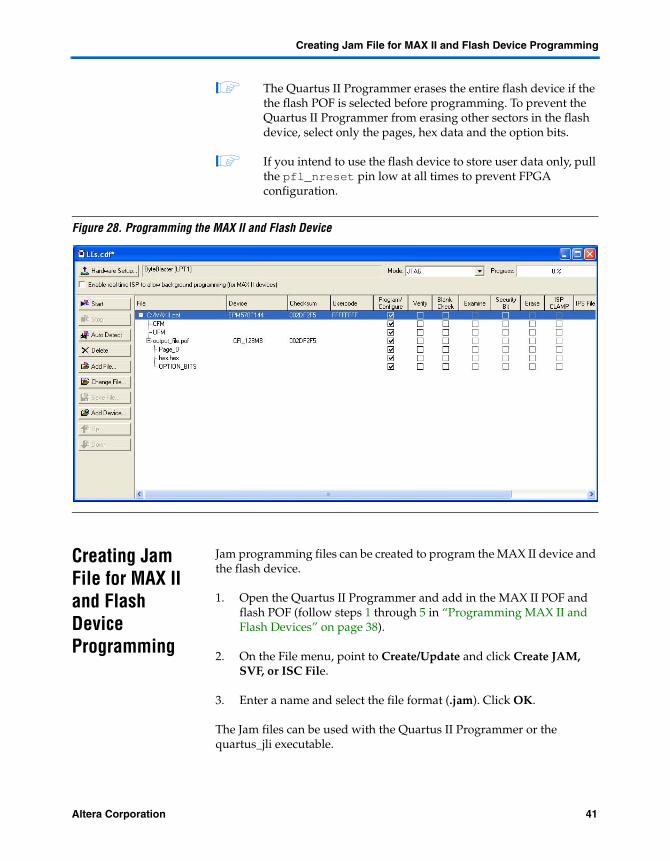
1 The Quartus II Programmer erases the entire flash device if the the flash POF is selected before programming. To prevent the Quartus II Programmer from erasing other sectors in the flash device, select only the pages, hex data and the option bits.
1 If you intend to use the flash device to store user data only, pull the pfl_nreset pin low at all times to prevent FPGA configuration.
Figure 28. Programming the MAX II and Flash Device
Creating Jam File for MAX II and Flash Device Programming
Jam programming files can be created to program the MAX II device and the flash device.
1. Open the Quartus II Programmer and add in the MAX II POF and flash POF (follow steps 1 through 5 in “Programming MAX II and Flash Devices” on page 38).
2. On the File menu, point to Create/Update and click Create JAM, SVF, or ISC File.
3. Enter a name and select the file format (.jam). Click OK.
The Jam files can be used with the Quartus II Programmer or the quartus_jli executable.
Altera Corporation 41
Using the Parallel Flash Loader with the Quartus II Software
1 Currently, Jam programming does not support flash programming if the flash programming IP is optimized for speed. The Jam file generated can still be used for programming the MAX II device, but not the flash device.
f For more information on the quartus_jli executable, refer to the AN 425: Using Command-Line Jam STAPL Solution for Device Programming.
PFL Configuration Simulation
With the correct simulation vectors, you can simulate the configuration part of the PFL using the Quartus II Simulator to understand the configuration behavior of the PFL. Simulation with the Quartus II Simulator can be performed using the Vector Waveform File (.vwf) and a simple VHDL file that represents a flash device. This VHDL file is available with this application note. With the correct input vectors supplied to the input of the PFL, you can see the correct output from the megafunction in the simulation waveform.
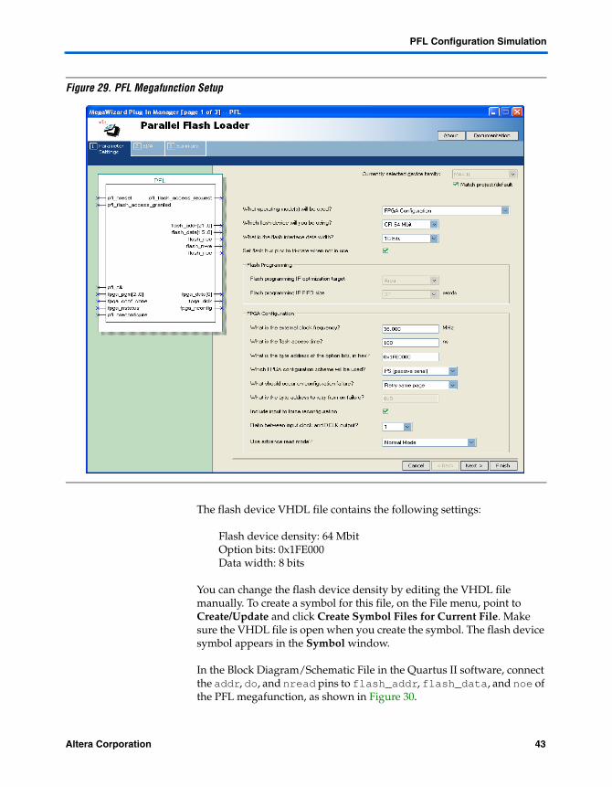
The rest of this section provides an example of a simulation for PFL configuration. Figure 29 shows the PFL megafunction setup for this example.
Before you start the simulation, you must instantiate the PFL megafunction and create a symbol for your flash device VHDL file in your design if you use block diagrams as the design entry. This example uses block diagrams as design entry.
42 Altera Corporation
PFL Configuration Simulation
Figure 29. PFL Megafunction Setup
The flash device VHDL file contains the following settings:
Flash device density: 64 MbitOption bits: 0x1FE000Data width: 8 bits
You can change the flash device density by editing the VHDL file manually. To create a symbol for this file, on the File menu, point to Create/Update and click Create Symbol Files for Current File. Make sure the VHDL file is open when you create the symbol. The flash device symbol appears in the Symbol window.
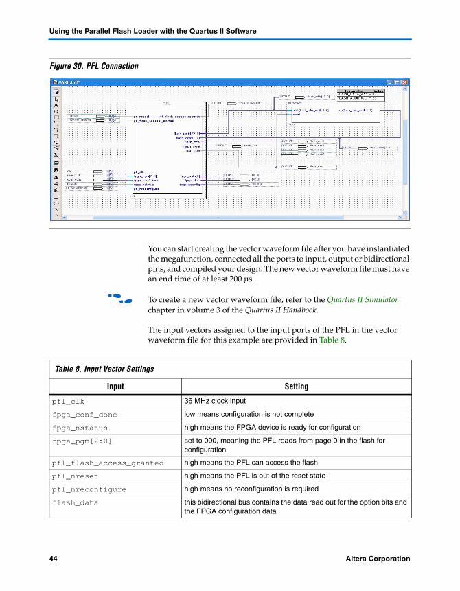
In the Block Diagram/Schematic File in the Quartus II software, connect the addr, do, and nread pins to flash_addr, flash_data, and noe of the PFL megafunction, as shown in Figure 30.
Altera Corporation 43
Using the Parallel Flash Loader with the Quartus II Software
Figure 30. PFL Connection
You can start creating the vector waveform file after you have instantiated the megafunction, connected all the ports to input, output or bidirectional pins, and compiled your design. The new vector waveform file must have an end time of at least 200 µs.
f To create a new vector waveform file, refer to the Quartus II Simulator chapter in volume 3 of the Quartus II Handbook.
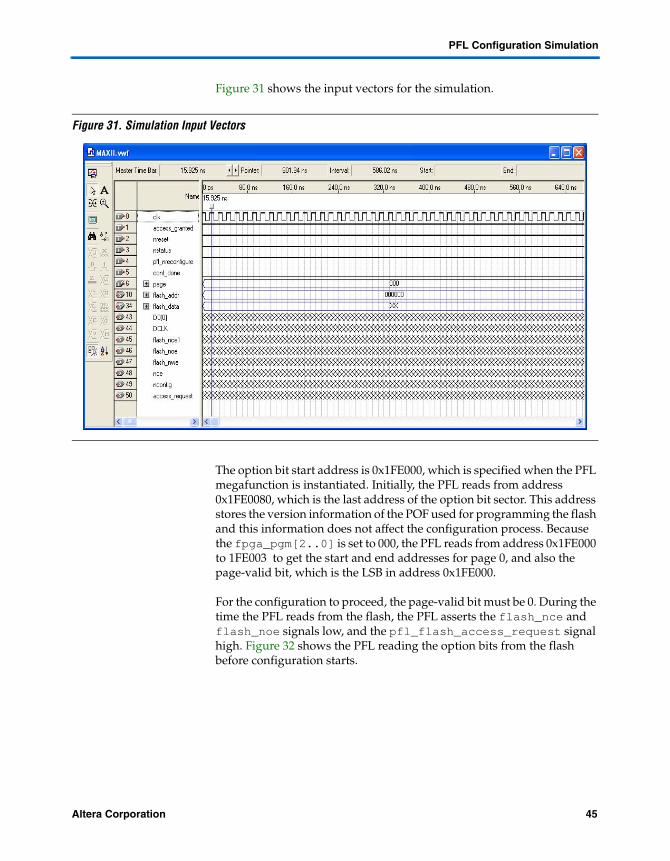
The input vectors assigned to the input ports of the PFL in the vector waveform file for this example are provided in Table 8.
Table 8. Input Vector Settings
Input Setting
pfl_clk 36 MHz clock input
fpga_conf_done low means configuration is not complete
fpga_nstatus high means the FPGA device is ready for configuration
fpga_pgm[2:0] set to 000, meaning the PFL reads from page 0 in the flash for configuration
pfl_flash_access_granted high means the PFL can access the flash
pfl_nreset high means the PFL is out of the reset state
pfl_nreconfigure high means no reconfiguration is required
flash_data this bidirectional bus contains the data read out for the option bits and the FPGA configuration data
44 Altera Corporation
PFL Configuration Simulation
Figure 31 shows the input vectors for the simulation.
Figure 31. Simulation Input Vectors
The option bit start address is 0x1FE000, which is specified when the PFL megafunction is instantiated. Initially, the PFL reads from address 0x1FE0080, which is the last address of the option bit sector. This address stores the version information of the POF used for programming the flash and this information does not affect the configuration process. Because the fpga_pgm[2..0] is set to 000, the PFL reads from address 0x1FE000 to 1FE003 to get the start and end addresses for page 0, and also the page-valid bit, which is the LSB in address 0x1FE000.
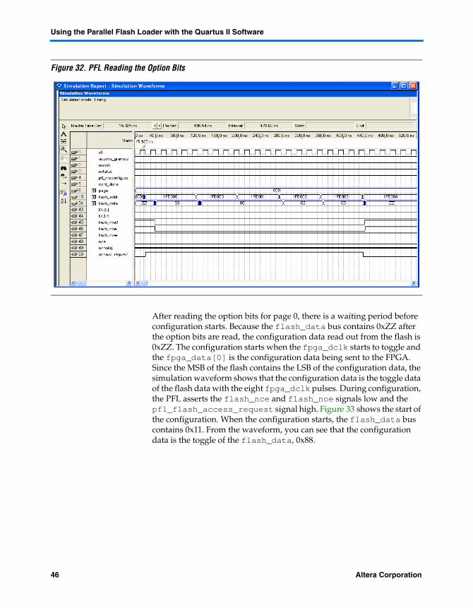
For the configuration to proceed, the page-valid bit must be 0. During the time the PFL reads from the flash, the PFL asserts the flash_nce and flash_noe signals low, and the pfl_flash_access_request signal high. Figure 32 shows the PFL reading the option bits from the flash before configuration starts.
Altera Corporation 45
Using the Parallel Flash Loader with the Quartus II Software
Figure 32. PFL Reading the Option Bits
After reading the option bits for page 0, there is a waiting period before configuration starts. Because the flash_data bus contains 0xZZ after the option bits are read, the configuration data read out from the flash is 0xZZ. The configuration starts when the fpga_dclk starts to toggle and the fpga_data[0] is the configuration data being sent to the FPGA. Since the MSB of the flash contains the LSB of the configuration data, the simulation waveform shows that the configuration data is the toggle data of the flash data with the eight fpga_dclk pulses. During configuration, the PFL asserts the flash_nce and flash_noe signals low and the pfl_flash_access_request signal high. Figure 33 shows the start of the configuration. When the configuration starts, the flash_data bus contains 0x11. From the waveform, you can see that the configuration data is the toggle of the flash_data, 0x88.
46 Altera Corporation
PFL Configuration Simulation
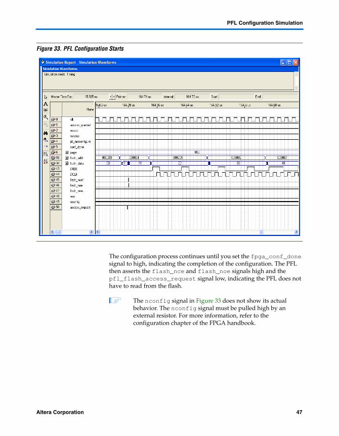
Figure 33. PFL Configuration Starts
The configuration process continues until you set the fpga_conf_done signal to high, indicating the completion of the configuration. The PFL then asserts the flash_nce and flash_noe signals high and the pfl_flash_access_request signal low, indicating the PFL does not have to read from the flash.
1 The nconfig signal in Figure 33 does not show its actual behavior. The nconfig signal must be pulled high by an external resistor. For more information, refer to the configuration chapter of the FPGA handbook.
Altera Corporation 47
Using the Parallel Flash Loader with the Quartus II Software
Conclusion The MAX II PFL feature enables you to use CFI flash memories and MAX II devices to store FPGA configuration data and control configuration of Altera FPGAs.
Referenced Documents
■ AN 341: Using the Design Security Feature in Stratix II and Stratix II GX Devices
■ AN 425: Using Command-Line Jam STAPL Solution for Device Programming
■ Configuration Handbook■ Nios II Flash Programmer User Guide■ Nios II Processor Reference Handbook■ Quartus II Simulator chapter in volume 3 of the Quartus II Handbook■ SOPC Builder Components chapter in volume 4 of the Quartus II
Handbook
48 Altera Corporation
Document Revision History
Document Revision History
Table 9 shows the revision history for this chapter.
Table 9. Document Revision History (Part 1 of 3)
Date and Document Version Changes Made Summary of Changes
May 2008v4.1
● Updated Table 1.● Changed the title for Page Mode Implementation to
“Page Implementation in Flash POF”● Added additional note to Table 3● Added ST Micro to the title of Figure 14 and Figure 15● Updated Table 7● Updated Figure 19● Updated Figure 29● Added a footnote under Figure 33.
—
October 2007v4.0
● Updated Table 1.● Removed Table 2.● Updated Figure 4.● Added Note (1) to Figure 5.● Updated Figure 6, Figure 10, Figures 12 through 15
and Figure 17.● Updated and reorganized order of pins appearing in
Table 3. Added Note (4).● Added new “PFL Design Example” section.● Updated equations in Table 6.● Under “Using the PFL in Quartus II Software” section,
updated Figure 17 through Figure 23, and Figure 25.● Added new “Creating Jam File for MAX II and Flash
Device Programming” section.● Under “PFL Configuration Simulation”, updated
Figure 29 and Figure 30.● Updated and reorganized order of pins appearing in
Table 7.
● Updated document for version 7.2 of the Quartus II software.
● Added new section on “PFL Design Example” and “Creating Jam File for MAX II and Flash Device Programming”.
Altera Corporation 49
Using the Parallel Flash Loader with the Quartus II Software
May 2007v3.0
● Updated Figure 1.● Updated Table 1.● Updated Table 2.● Updated Auto Mode information in “Programming the
CFI Flash” section.● Updated Figure 6.● Added new “PFL Design Example” section.● Updated Table 3 and added three PFL signals and a
table note.● Updated Table 6 and added note.● Updated Figure 18.● Added new Table 7 in step 7 in “Instantiating the PFL
Megafunction in Quartus II Software” section.● Updated Figures 19, 20, 21, and 22.● Updated step 7 in “Converting the SOF(s) to a POF
for the Flash Device” section.● Added new Figure 24.
● Updated document for version 7.1 of the Quartus II software.
● Added new section on “PFL Configuration Simulation”.
December 2006v2.1
● Updated Table 1 and accompanying notes.● Updated Table 2 and accompanying note.● Updated information for Auto Mode in “Page
Implementation in Flash POF” section.● Updated Figure 5 and added new note to figure.● Updated Figure 6.● Updated Table 3.● Added new section on “PFL Configuration Time”.● Added new section on “PFL and Flash Address
Mapping”. ● Updated Step 7 in “Instantiating the PFL
Megafunction in Quartus II Software” section.● Updated Figure 19, Figure 20 and Figure 21 in
“Instantiating the PFL Megafunction in Quartus II Software” section.
● Updated Step 2 and added Steps 3 and 4 in “Programming MAX II and Flash Devices” section.
● Updated Figure 25, and added new Figure 26 and Figure 27 in “Programming MAX II and Flash Devices” section.
● Updated Figure 28.
—
Table 9. Document Revision History (Part 2 of 3)
Date and Document Version Changes Made Summary of Changes
50 Altera Corporation
Document Revision History
October 2006v2.0
● Updated Table 1 and accompanying notes.● Updated Figure 5.● Updated Table 2.● Updated hand paragraph in “Page Mode
Implementation” section.● Updated material in “Using the PFL in the Quartus II
Software” section.● Updated Figure 16.● Updated hand paragraph in “Instantiating the PFL
Megafunction in the Quartus II Software” section.● Updated step 7 d in the “Converting the SOF(s) to a
POF for the Flash Device” section.● Updated hand paragraph in the “Programming Max II
and Flash Devices” section.
—
Table 9. Document Revision History (Part 3 of 3)
Date and Document Version Changes Made Summary of Changes
Altera Corporation 51
101 Innovation DriveSan Jose, CA 95134www.altera.comLiterature Services:[email protected]
Copyright © 2008 Altera Corporation. All rights reserved. Altera, The Programmable Solutions Company,the stylized Altera logo, specific device designations, and all other words and logos that are identified astrademarks and/or service marks are, unless noted otherwise, the trademarks and service marks of AlteraCorporation in the U.S. and other countries. All other product or service names are the property of theirrespective holders. Altera products are protected under numerous U.S. and foreign patents and pendingapplications, maskwork rights, and copyrights. Altera warrants performance of its semiconductor productsto current specifications in accordance with Altera's standard warranty, but reserves the right to makechanges to any products and services at any time without notice. Altera assumes no responsibility or liabilityarising out of the application or use of any information, product, or service describedherein except as expressly agreed to in writing by Altera Corporation. Altera customersare advised to obtain the latest version of device specifications before relying on anypublished information and before placing orders for products or services.