Embed Size (px)
Citation preview
www.linx-consulting.com
OUTLOOK FOR ADVANCED CLEANS Business of Cleans
April 9, 2018
Mike Corbett Linx Consulting Inc.

www.linx-consulting.com
Outline
• Introduction to Linx Consulting
• Semi Industry Outlook
• Materials Challenges
• Impact on Suppliers
• Conclusions

www.linx-consulting.com
Introduction to Linx Consulting

www.linx-consulting.com
Linx Consulting
North America
China
SEA & India
Europe
Japan
Korea
Taiwan
1. We help our clients to succeed by creating know ledge and developing unique insights at the intersection of electronic thin film processes and the chemicals industry on a global basis
2. The know ledge is based on a core understanding of the semiconductor device technology; manufacturing processes and roadmaps; and the global structural industry dynamics
3. This know ledge is leveraged to create advanced models, simulations and real-world forecasts
4. Our perspectives are by direct research and leveraging our extensive experience throughout the global industry value chain
Finance &Technology
Raws & Chemicals Equipment Services End-users &
Consortia
www.linx-consulting.com
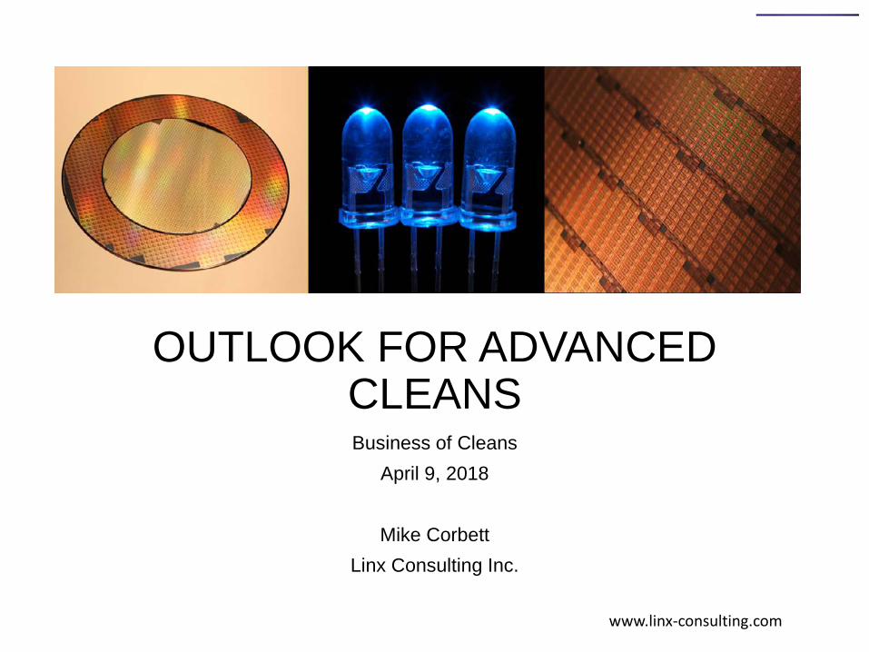
MSI Breakdown & Forecasts

www.linx-consulting.com
Linx Consulting Service Portfolio

www.linx-consulting.com
Semi Industry Outlook

www.linx-consulting.com
Industry Trends Summary
• Healthy GDP growth rates expected in all major regions
• Record levels of CapEx reflect very high utilization (>95%) across both 200 mm and 300 mm fabs, driven by record demand for Logic and 3D NAND chips
• Fifteen IDMs exceed $1B spend in 2017, spanning US-based (Intel, Micron, Global Foundries), European (ST Micro, Infineon) and Asian companies
• Samsung remains the industry top spender, with $20B CapEx forecasted for both 2017 and 2018
• Geographically, new fab construction is highly concentrated in Asia, with China investment dominating the list
• Several trends support such rapid industry expansion • Some are already driving significant volume of chips, e.g. next-generation communication
networks, automotive electronics/ADAS, and Internet of Things/IoT • Others are nascent and will fuel this growth for years to come, e.g. Artificial
Intelligence/AI, VR/AR technologies, and autonomous vehicles

www.linx-consulting.com
Economic Drivers
U.S Business Investment
-2
-1
0
1
2
3
4
5
07 08 09 10 11 12 13 14 15 16 17 18 19
ESF 2017 Q4December 17 Update
*World: 85 major economies History: World Bank, US Bureau of Economic Analysis Forecast: Hilltop Economics, Consensus Forecasts Nov & Dec 17
Perc
ent C
hang
e
World* Real GDP Growth2016: 2.3% 2017: 3.0% 2018: 3.1%
-20
-15
-10
-5
0
5
10
15
20
06 07 08 09 10 11 12 13 14 15 16 17 18 19
U.S. Business Investment (P&E)U.S. Technology Equipment Investment
%CH
VS YR
AGO
, 4QM
A
Shaded Areas Indicate U.S. RecessionsHistory: U.S. Bureau of Ecnomic Analysis, ($)Forecast: Hilltop Economics December 2017

www.linx-consulting.com
Linx WFM Equity Index

www.linx-consulting.com
Latest MSI Forecast by ESF Model

www.linx-consulting.com
Record Levels of Capex
Capacity Utilization for 200mm and 300mm fabs > 95% in 2017

www.linx-consulting.com
Key Growth Drivers: NAND, DRAM and Foundry
3DN and Logic driving growth. Vertical scaling helps drive Materials Growth

www.linx-consulting.com
Materials Challenges

www.linx-consulting.com
Trends Impacting WFM Suppliers
Sources: Intel, ICMTIA, AMAT, ICKnowledge
www.linx-consulting.com
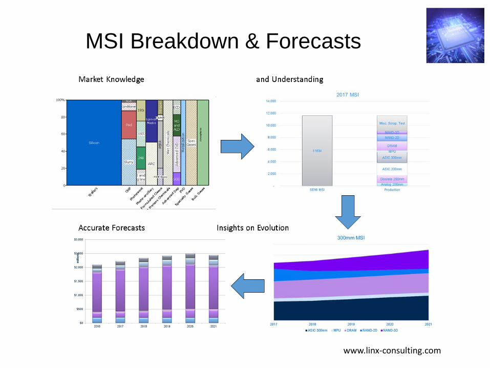
Materials Opportunities
Demand Drivers • CuBS demand increasing in Logic Interconnect
• Limitations of current architectures
• FinFET gate deposition • GAA Nanowire development • High mobility materials
• Memory technology extension • 3D-NAND growth • DRAM capacitor dielectric • Novel architectures
• Pitch doubling and quadrupling • Low temperature spacers
• Lithography aids
Opportunities • Possible changes in conductor metal
• Cu Co Barrier Co plating
• 3D-NAND aspect ratio • Hard mask technology • 2D stair-step
• Novel process development • Multi color, self aligning etch • CVD Continuous etch • ALD ALE
• Self Assembling Materials for selective processes
• Few new PVD applications • 3DXpoint / MRAM?
• Selective Deposition • Self Assembling Materials • Selective Deposition

www.linx-consulting.com
The Cleaning Market Environment • Technology – The cleaning
challenge continues to increase, and new, smaller device structures and materials will increase the difficulty of preparing the wafer for the next process step. Enabling technologies are valued significantly more by end-users than “like” or “me too” products.
• Proliferation of novel materials in gate architecture, memory cell technology, interconnect and packaging is adding complexity in material choice and formulation.
• Increased Customization – Customers are increasingly specifying custom products for layer specific problems.
(PM: Patterning Materials)
(IL: InterfaceLayer)sSOI/GeOI
Ge IL III-V ILGaN InSb
InGaAs Ge
STORu
Other PM's EUV
Other PM's EUV
Co Si(C)P
Co Si(C)P
FDSOISiC
FDSOISiC
Air SiCO
Air SiCO
LaO LaOLT SiO LT SiO
SiCN SiCN SiCNTiAlC MG
ZrO Hf(Si)O
AlO
TiAlC MGZrO
Hf(Si)OAlO
TiAlC MGZrO
Hf(Si)OAlO
pSiOC pSiOC pSiOCSOI SOI SOI
SiGe(B)TaO SOG
TaO SOG
SiGe(B)TaO SOG
SiGe(B)TaO SOG
SiOCTa/TaN
Cu SiOF
SiOCTa/TaN
Cu SiOF
SiOCTa/TaN
Cu SiOF
SiOCTa/TaN
Cu SiOF
TiSi PtSi
TiSi PtSi
TiSi PtSi
TiSi PtSi
TiSi PtSi
TiW TiW TiW/TiN TiN TiN TiNWSi, MoSi WSi, W WSi, W W W W
AlBPSG
AlBPSG
AlBPSG
AlBPSG
AlBPSG
AlBPSG
AlBPSG
AlSiO, SiN SiO, SiN SiO, SiN SiO, SiN SiO, SiN SiO, SiN SiO, SiN SiO, SiN
Si Si Si Si Si Si Si Si
1960 1970 1980 1990 2000 2010 2015 2020(*)
(*): Projection
Patterning RelatedBEOLFEOLStarting Materials
New Materials and Architectures Enable Moore’s Law
www.linx-consulting.com
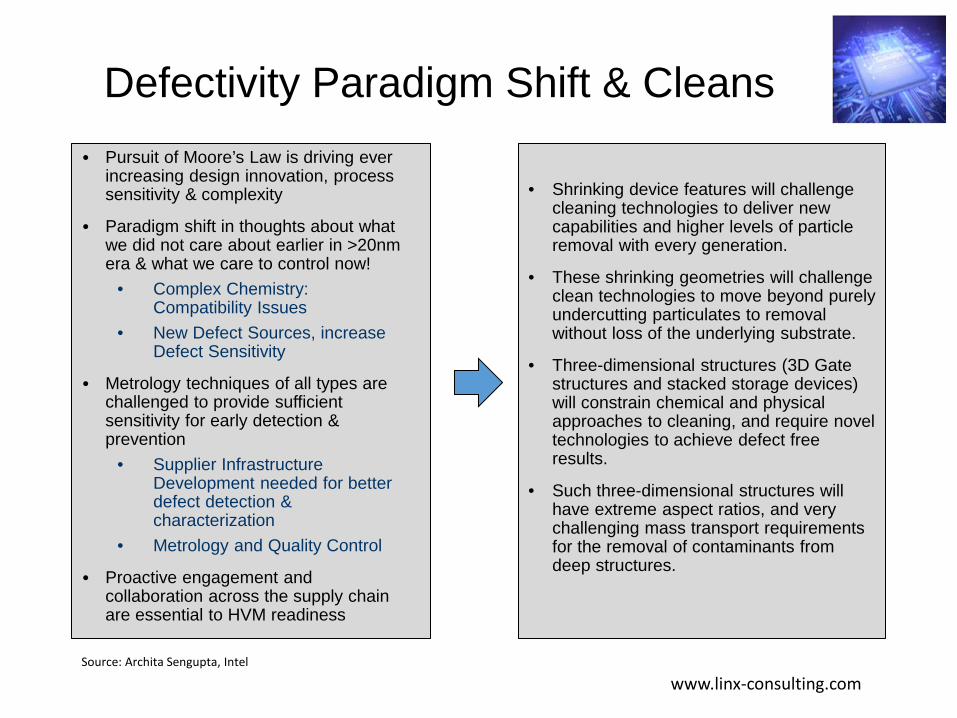
Defectivity Paradigm Shift & Cleans • Pursuit of Moore’s Law is driving ever
increasing design innovation, process sensitivity & complexity
• Paradigm shift in thoughts about what we did not care about earlier in >20nm era & what we care to control now!
• Complex Chemistry: Compatibility Issues
• New Defect Sources, increase Defect Sensitivity
• Metrology techniques of all types are challenged to provide sufficient sensitivity for early detection & prevention
• Supplier Infrastructure Development needed for better defect detection & characterization
• Metrology and Quality Control
• Proactive engagement and collaboration across the supply chain are essential to HVM readiness
• Shrinking device features will challenge cleaning technologies to deliver new capabilities and higher levels of particle removal with every generation.
• These shrinking geometries will challenge clean technologies to move beyond purely undercutting particulates to removal without loss of the underlying substrate.
• Three-dimensional structures (3D Gate structures and stacked storage devices) will constrain chemical and physical approaches to cleaning, and require novel technologies to achieve defect free results.
• Such three-dimensional structures will have extreme aspect ratios, and very challenging mass transport requirements for the removal of contaminants from deep structures.
Source: Archita Sengupta, Intel

www.linx-consulting.com
Trends - WFM Spend at Advanced Nodes
Source: Linx, IC Knowledge, Intel
www.linx-consulting.com
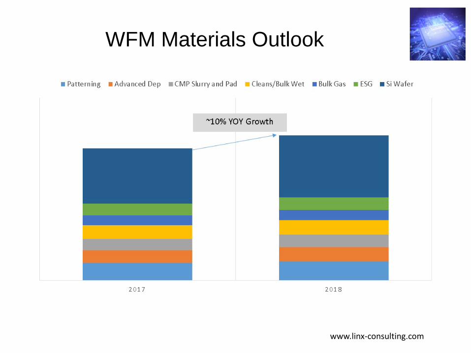
WFM Materials Outlook

www.linx-consulting.com
Advanced Cleans Outlook

www.linx-consulting.com
Paths Forward for Consumables
ADVANCED / SPECIALTY • Enable novel architectures and litho
schemes: • 3DN • FinFET • Horizontal Nano wire
• Enable new memory technologies
• PCM • STT MRAM
• Enable new BEOL materials
• Cobalt, Ru • Alternative/self forming barrier
• Solve productivity and defectivity problems
COMMODITY • Have evolved from current materials base
• Need to be drop-in ready
• Are readily copied
• Will compete based on cost
• Most impacted by changes to business
model

www.linx-consulting.com
Impact on Suppliers
www.linx-consulting.com
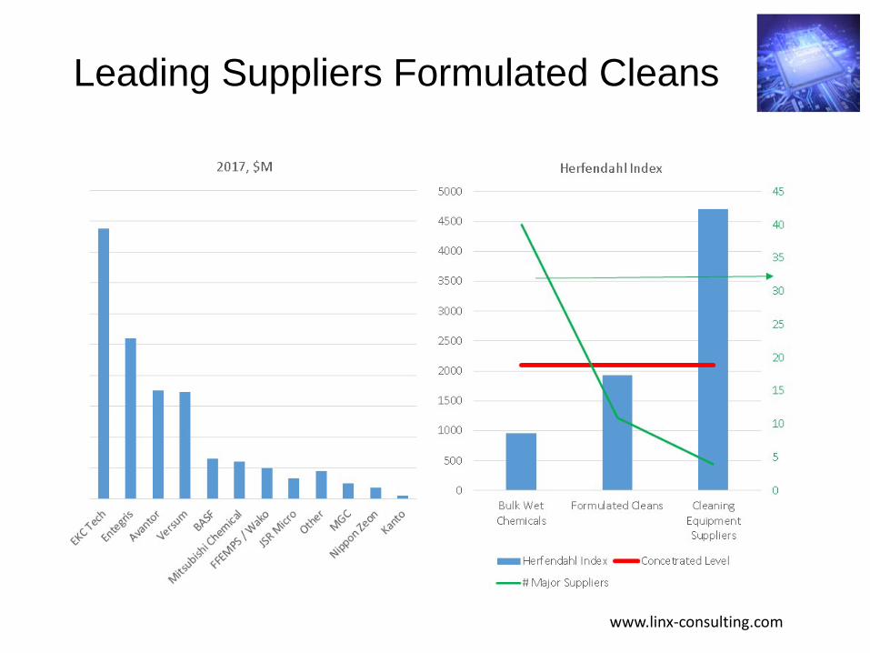
Leading Suppliers Formulated Cleans

www.linx-consulting.com
Regional & Structural Trends
• Cabot Microelectronics – NexPlanar
• Fujimi Collaboration
• FujiFilm EM – Ultra Pure + Wako
• Wonik – Nova-Kem
• NATA - Kempur
• Air Liquide – AirGas + Voltaix
• Air Products – Versum Materials spinout
• SK - OCIM + Tri-Chem
China • Leveraged government equity
positions to enable significant sized acquisitions
• Continued acquisition activity from multiple companies.
• Acquisitions along the line of key product areas:
• Silicon • Gases • Lithography materials • Advanced deposition
materials Korea • Korean companies also looking
to change business model • Gain international market access
• Dow Chemical – DuPont + Dow Corning
• Global Wafer - SunEdison
• Yoke – UPChem
• Versum - Dynaloy
• SK Holding – LG Siltron + OCIM
• Linde + Praxair
• Avantor - Gelest
Recent Transactions

www.linx-consulting.com
Top Tier WFM Suppliers

www.linx-consulting.com
Conclusions

www.linx-consulting.com
Conclusions
• Sustainable strong growth outlook anticipated for several years
• 3D structures and new materials will continue to drive semiconductor technology advancement at 1Xnm and beyond.
• 200mm and older wafer fab is expected to remain at high levels of capacity utilization over the next several years. Productivity will be a major driver
• Concentrated customer base and tool supplier base, along with increasing barriers to serve end-users will drive WFM consolidation
• New capacity in China will enable new suppliers who will initially compete with special commodities
• Expect Korea to focus more effort on specialty chemicals