Embed Size (px)
Citation preview

THE WAFER FAB CLEANS IN SEMICONDUCTOR INDUSTRY FROM A MATERIALS SUPPLIER PERSPECTIVE
Tianniu Rick Chen, Ph.D.General ManagerSP&C Business (Surface Preparation & Cleans)
OUTLINE
• Market drivers and challenges• Technology advancements and challenges• Questions and answers
© Versum Materials 2018
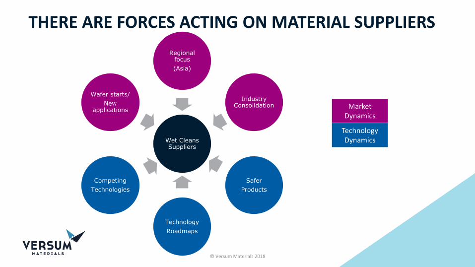
THERE ARE FORCES ACTING ON MATERIAL SUPPLIERS
© Versum Materials 2018
Wet Cleans Suppliers
Regional focus
(Asia)
Industry Consolidation
Safer
Products
Technology
Roadmaps
Competing
Technologies
Wafer starts/
New applications
MarketDynamics
TechnologyDynamics
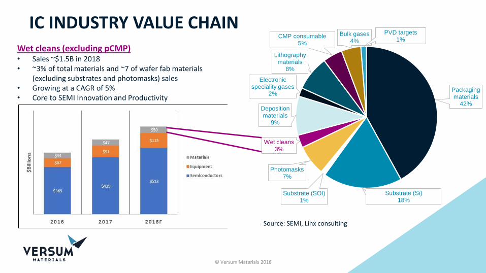
IC INDUSTRY VALUE CHAINWet cleans (excluding pCMP)• Sales ~$1.5B in 2018• ~3% of total materials and ~7 of wafer fab materials
(excluding substrates and photomasks) sales• Growing at a CAGR of 5%• Core to SEMI Innovation and Productivity
Source: SEMI, Linx consulting
© Versum Materials 2018
Packaging materials
42%
Substrate (Si)18%
Substrate (SOI)1%
Photomasks7%
Wet cleans3%
Deposition materials
9%
Electronic speciality gases
2%
Lithography materials
8%
CMP consumable5%
Bulk gases4%
PVD targets1%
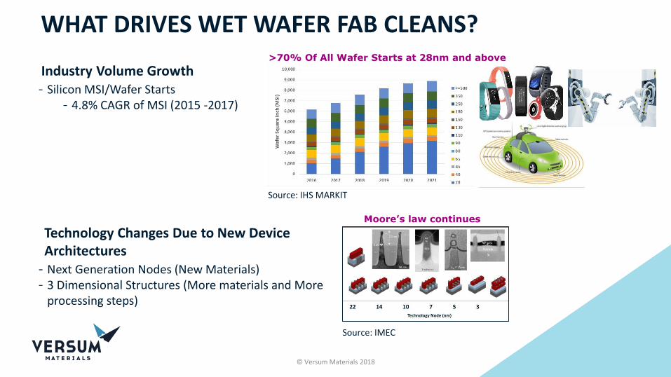
WHAT DRIVES WET WAFER FAB CLEANS?
Industry Volume Growth- Silicon MSI/Wafer Starts
- 4.8% CAGR of MSI (2015 -2017)
Source: IMEC
© Versum Materials 2018
Technology Changes Due to New Device Architectures- Next Generation Nodes (New Materials)- 3 Dimensional Structures (More materials and More
processing steps)
>70% Of All Wafer Starts at 28nm and above
Moore’s law continues
Source: IHS MARKIT
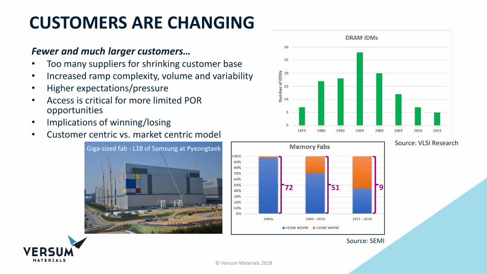
CUSTOMERS ARE CHANGING
Fewer and much larger customers…• Too many suppliers for shrinking customer base• Increased ramp complexity, volume and variability • Higher expectations/pressure• Access is critical for more limited POR
opportunities• Implications of winning/losing• Customer centric vs. market centric model
© Versum Materials 2018
72 51 9
Giga-sized fab - L18 of Samsung at PyeongtaekSource: VLSI Research
Source: SEMI
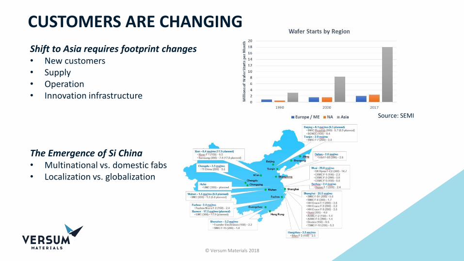
CUSTOMERS ARE CHANGING
Shift to Asia requires footprint changes• New customers• Supply• Operation• Innovation infrastructure
© Versum Materials 2018
The Emergence of Si China• Multinational vs. domestic fabs• Localization vs. globalization
Source: SEMI
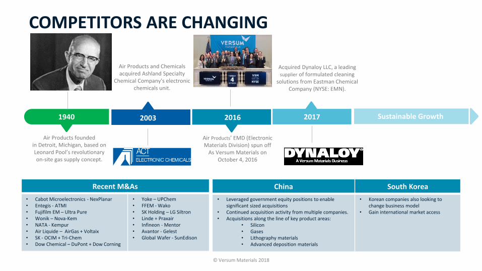
COMPETITORS ARE CHANGING
© Versum Materials 2018
Air Products and Chemicals acquired Ashland Specialty
Chemical Company's electronic chemicals unit.
Air Products foundedin Detroit, Michigan, based on Leonard Pool’s revolutionary on-site gas supply concept.
Acquired Dynaloy LLC, a leading supplier of formulated cleaning
solutions from Eastman Chemical Company (NYSE: EMN).
Air Products’ EMD (Electronic Materials Division) spun off
As Versum Materials on October 4, 2016
2003 2016 Increase 80%1940 2017 Sustainable Growth
Recent M&As
• Cabot Microelectronics - NexPlanar• Entegis - ATMI• Fujifilm EM – Ultra Pure• Wonik – Nova-Kem • NATA - Kempur • Air Liquide – AirGas + Voltaix• SK - OCIM + Tri-Chem• Dow Chemical – DuPont + Dow Corning
• Yoke – UPChem• FFEM - Wako • SK Holding – LG Siltron• Linde + Praxair• Infineon - Mentor• Avantor - Gelest• Global Wafer - SunEdison
China South Korea
• Leveraged government equity positions to enable significant sized acquisitions
• Continued acquisition activity from multiple companies.• Acquisitions along the line of key product areas:
• Silicon• Gases• Lithography materials• Advanced deposition materials
• Korean companies also looking to change business model
• Gain international market access
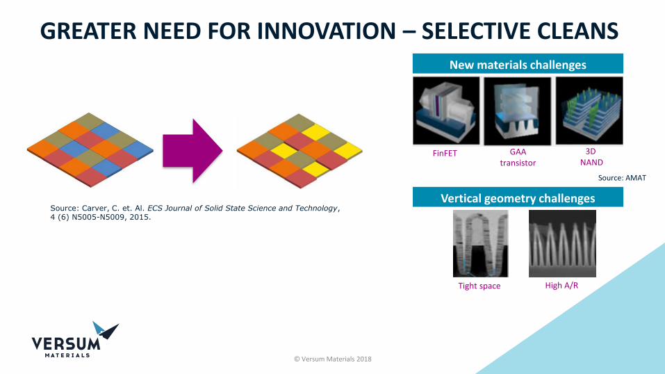
GREATER NEED FOR INNOVATION – SELECTIVE CLEANS
© Versum Materials 2018
Source: AMAT
Source: Carver, C. et. Al. ECS Journal of Solid State Science and Technology, 4 (6) N5005-N5009, 2015.
New materials challenges
Vertical geometry challenges
Tight space High A/R
FinFET GAAtransistor
3D NAND

GREATER NEED FOR INNOVATION – SELECTIVE CLEANS(CONTINUED)
© Versum Materials 2018
Competing technology of wet cleaning – ALE (Atomic Layer Etching) of SiNx
Source: Hitachi, The 232nd Electrochemical Society (ECS) Meeting , October 1 to 5, 2017, National Harbor, Maryland.
Source: Sherpa, S., et. al. Journal of Vacuum Science & Technology A: Vacuum, Surfaces, and Films 35, 05C310, 2017.
Pre- Pre-Post- Post-
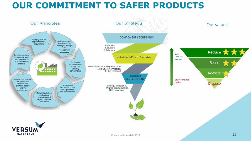
OUR COMMITMENT TO SAFER PRODUCTS
11© Versum Materials 2018
Our values

CRITERIA FOR SUCCESS GOING INTO THE 2020S
▪ Customer Relationships
▪ Diversified Portfolio
▪ Innovation Capabilities and Intellectual Property
▪ Global Infrastructure and Reliable Supply
SEMI Next
GenerationSpecialty MaterialsSupplier
© Versum Materials 2018
Grace, Elegance… and Fortitude
THANK YOU
© Versum Materials 2018
Wednesday, April 11th, 2018, 10:40 AM:
“Development of Wet-Etch Chemistries for Tungsten Word-line Recess” by C.K. Ge, Versum Materials