Embed Size (px)
Citation preview
1
Photonic Materials: Context, Principles, Selected
Applications
Professor Mark P. AndrewsDepartment of Chemistry
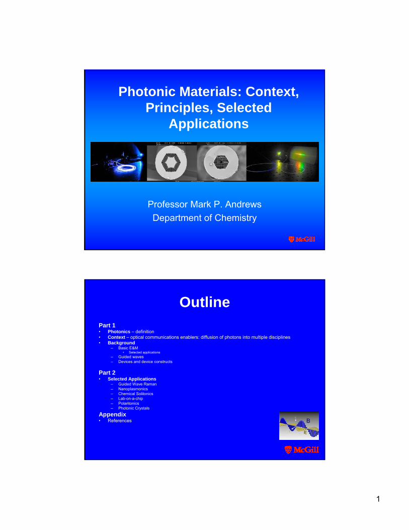
OutlinePart 1• Photonics – definition• Context – optical communications enablers: diffusion of photons into multiple disciplines• Background
– Basic E&M• Selected applications
– Guided waves– Devices and device constructs
Part 2• Selected Applications
– Guided Wave Raman– Nanoplasmonics– Chemical Solitonics– Lab-on-a-chip– Polaritonics– Photonic Crystals
Appendix• References
2
source: Photonics Spectra magazine
3
"Photonics is the technology of generating and harnessing light and other forms of radiant energy whose quantum unit is the photon. The science includes light emission, transmission, deflection, amplification and detection by optical components and instruments, lasers and other light sources, fibre optics, electro-optical instrumentation, related hardware and electronics, and sophisticated systems. The range of applications of photonics extends from energy generation to detection to communications and information processing.“
- The Photonics Dictionary, Laurin Publishing.
Photonic Context
Mapping how people use the WebBen Fry’s Organic Information Design
MIT
4
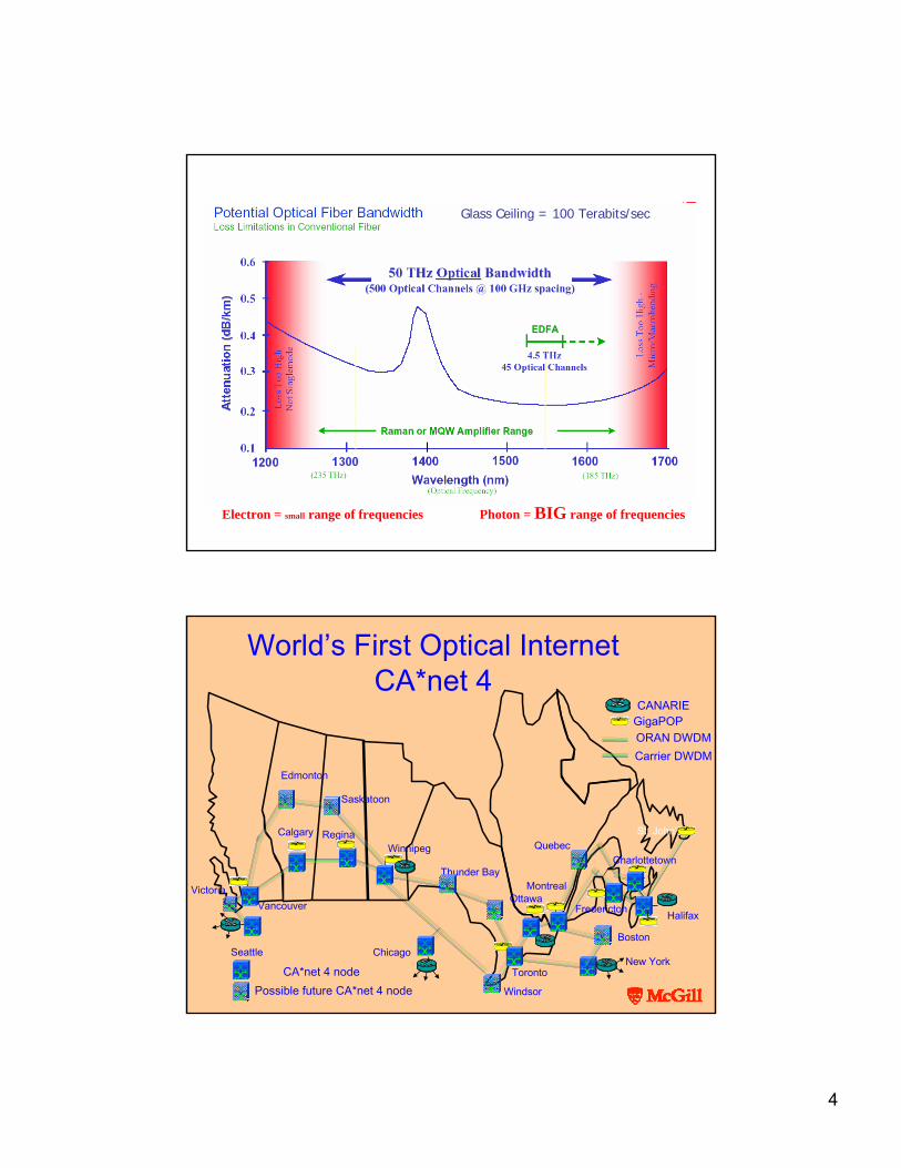
Glass Ceiling = 100 Terabits/sec
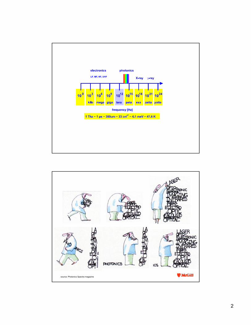
Electron = small range of frequencies Photon = BIG range of frequencies
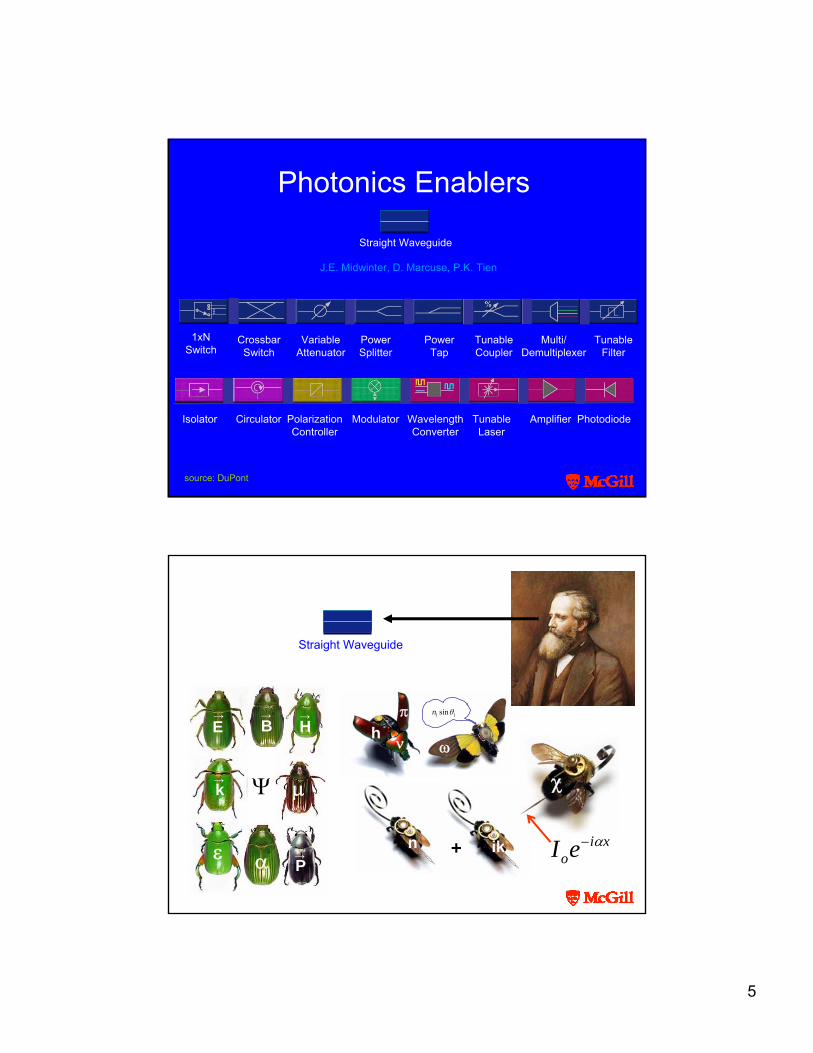
World’s First Optical InternetCA*net 4
Calgary ReginaWinnipeg
OttawaMontreal
Toronto
Halifax
St. John’s
Fredericton
Charlottetown
ChicagoSeattleNew York
CANARIEGigaPOPORAN DWDMCarrier DWDM
Thunder Bay
CA*net 4 nodePossible future CA*net 4 node
Quebec
Windsor
Edmonton
Saskatoon
VictoriaVancouver
Boston
5
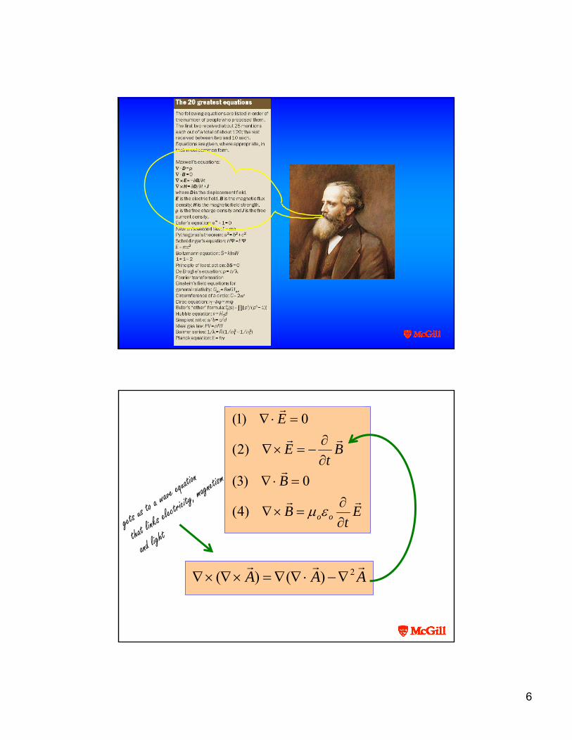
Photonics Enablers
1xNSwitch
CrossbarSwitch
VariableAttenuator
PowerSplitter
PowerTap
TunableCoupler
Multi/Demultiplexer
TunableFilter
Isolator Circulator PolarizationController
Modulator WavelengthConverter
TunableLaser
Amplifier Photodiode
source: DuPont
J.E. Midwinter, D. Marcuse, P.K. Tien
Straight Waveguide
E→
B→
k→
H→
μ
ε α
Ψ
P→
hν
π
ω
n ik+
χ
xioeI α−
Straight Waveguide
11 sinθn
6
Et
B
B
Bt
E
E
oo ∂∂
=×∇
=⋅∇∂∂
−=×∇
=⋅∇
εμ)4(
0)3(
)2(
0)1(
AAA 2)()( ∇−⋅∇∇=×∇×∇
gets us to
a wave e
quation
that links
electrici
ty, magne
tism
and light
7
Et
Btt
B
ofRHS
EEEE
ofLHS
tBE
oo 2
2
22
)(
)2(
)()(
)2(
)(
∂∂
−=×∇∂∂
−=⎟⎟⎠
⎞⎜⎜⎝
⎛∂∂
−×∇
∇−=∇−⋅∇∇=×∇×∇
⎟⎟⎠
⎞⎜⎜⎝
⎛∂∂
−×∇=×∇×∇
εμ
equal,so
Et
E oo 2
22
∂∂
=∇ εμ
Et
E oo 2
22
∂∂
=∇ εμ
Bt
B oo 2
22
∂∂
=∇ εμ
ftv
f 2
2
22 1
∂∂
=∇
displacement
velocity
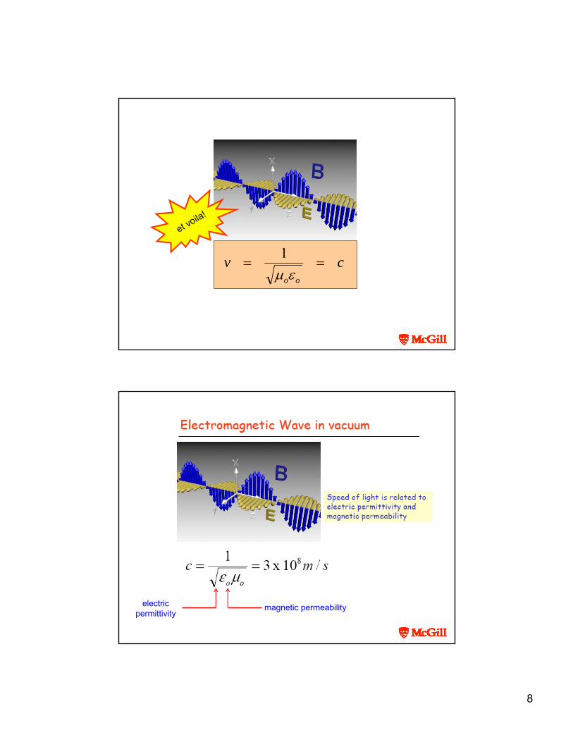
8
cvoo
==εμ
1
et voila!
magnetic permeabilityelectricpermittivity
magnetic fieldelectric field
Electromagnetic wave
λ
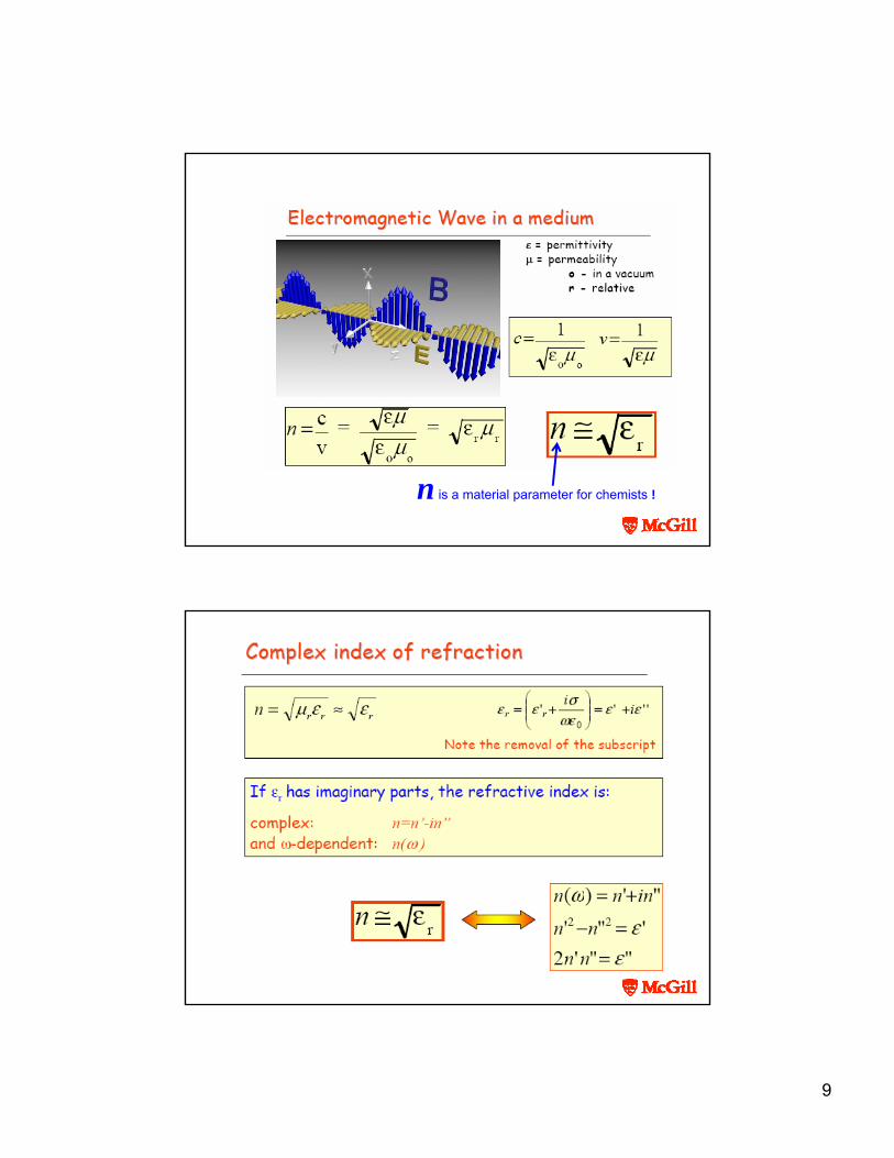
9
n is a material parameter for chemists !
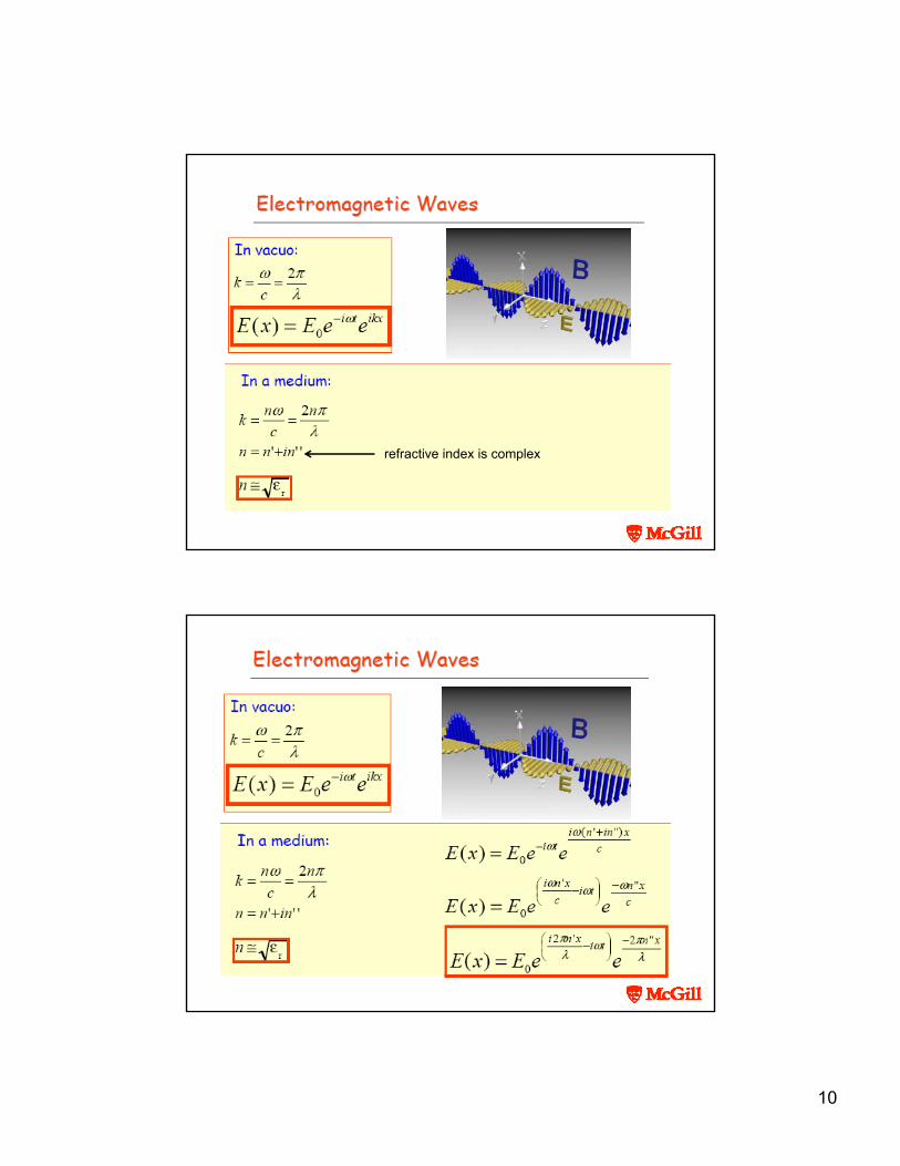
10
refractive index is complex
11
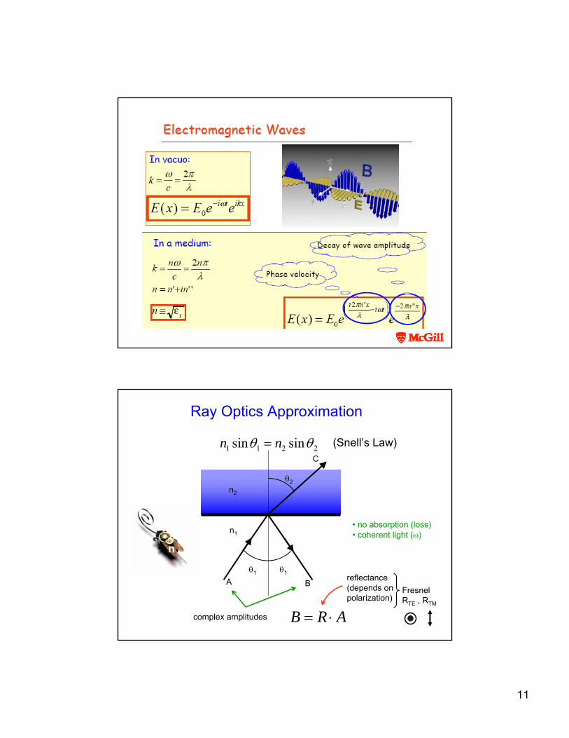
θ2n2
n1
θ1 θ1
A B
C
• no absorption (loss)• coherent light (ω)
2211 sinsin θθ nn = (Snell’s Law)
complex amplitudes ARB ⋅=
reflectance(depends on polarization)
Ray Optics Approximation
n
FresnelRTE , RTM
12
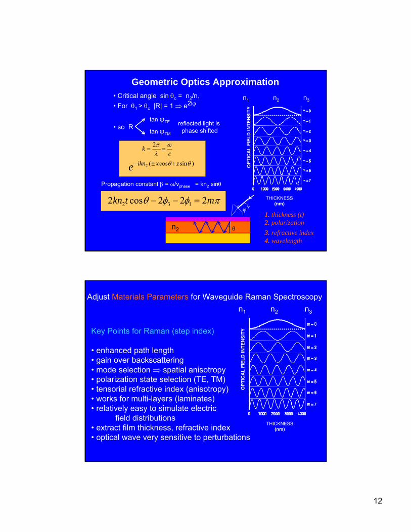
Geometric Optics Approximation
OP
TIC
AL
FIE
LD
INT
EN
SIT
Y
THICKNESS (nm)
n1 n2 n3
θ
ϕ
n2
1. thickness (t)2. polarization3. refractive index4. wavelength
• Critical angle sin θc = n2/n1
• For θ1 > θc |R| = 1 ⇒ e2iϕ
• so R tan ϕTE
tan ϕTM
reflected light is phase shifted
ck ω
λπ==
2
)sincos(2 θθ zxikne +±−
Propagation constant β = ω/vphase = kn2 sinθ
πφφθ mtkn 222cos2 132 =−−
OP
TIC
AL
FIE
LD
INT
EN
SIT
Y
THICKNESS (nm)
n1 n2 n3
Key Points for Raman (step index)
• enhanced path length • gain over backscattering• mode selection ⇒ spatial anisotropy• polarization state selection (TE, TM)• tensorial refractive index (anisotropy)• works for multi-layers (laminates)• relatively easy to simulate electric
field distributions• extract film thickness, refractive index• optical wave very sensitive to perturbations
Adjust Materials Parameters for Waveguide Raman Spectroscopy
13
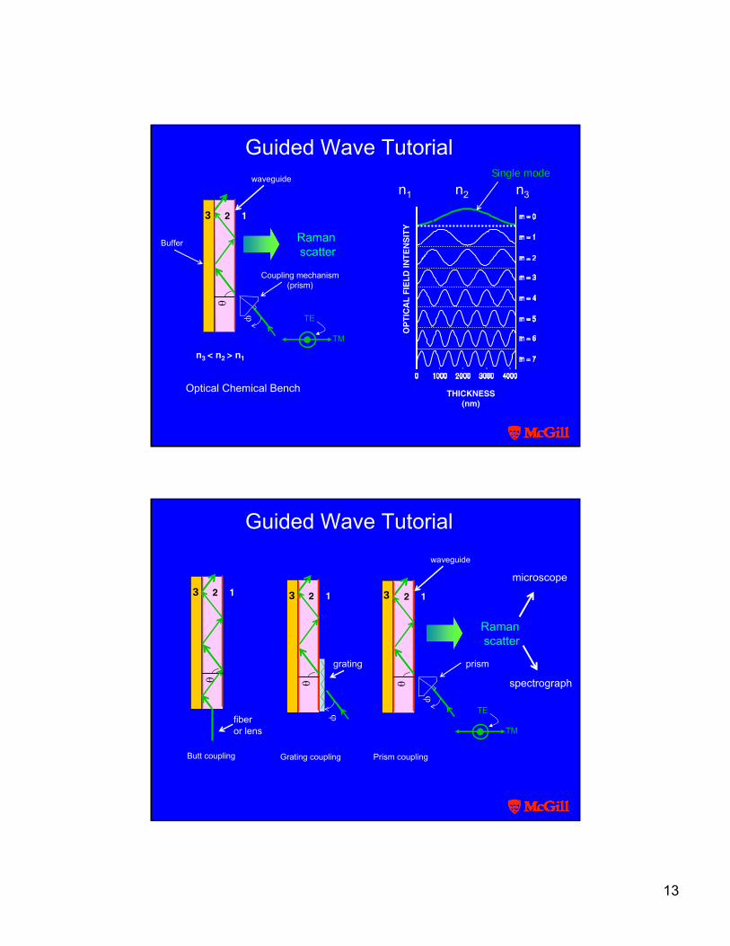
Guided Wave Tutorial
n3 < n2 > n1
θ
ϕ
123
Coupling mechanism(prism)
Buffer
waveguide
TM
TE
3
Optical Chemical Bench
Single mode
OP
TIC
AL
FIE
LD
INT
EN
SIT
Y
THICKNESS (nm)
Raman scatter
n1 n2 n3
Guided Wave Tutorial
Prism coupling
TM
TE
Raman scatter
θ
ϕ
123
waveguide
3
θ
ϕ
1233
Grating coupling
microscope
spectrograph
grating
θ
1233
Butt coupling
fiberor lens
prism
14
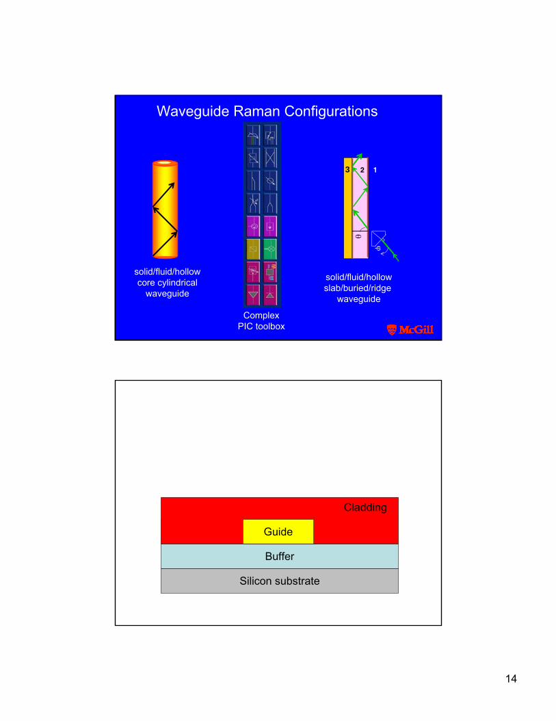
Waveguide Raman Configurations
θ
ϕ1233
solid/fluid/hollowcore cylindrical
waveguide
solid/fluid/hollowslab/buried/ridge
waveguide
ComplexPIC toolbox
Silicon substrate
Buffer
Guide
UV
Photomask
Wet Etch
Cladding
Guide
15
OCM Module
DEMUX
* * *
Ch 1Ch 2
Ch 1, Ch 2, …, Ch 16
* * *
DETECTORARRAY
AMPLI-FIER
* * *
Packaged Device Interior
Functional Diagram
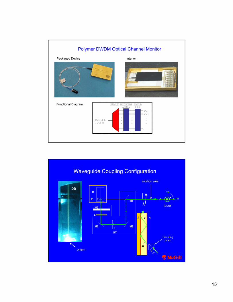
Polymer DWDM Optical Channel Monitor
Waveguide Coupling Configuration
M1
M2M3
L
λ/2
P
GT
H
θ
ϕ
123
Couplingprism
TM
TE
3
rotation axis
laser
prism
Si
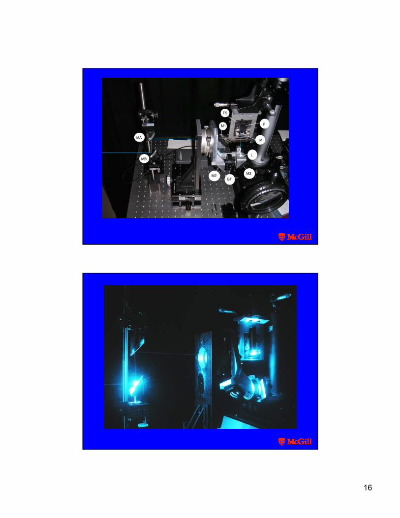
16
17
Strategies must be combined . . .
Simulationslab, cylinder
numerical BPM(optical loss)
Microfabrication(simple/complex)
Materials(anything that
will guide)
Opticalcoupling
DetectionScheme
Specialcells
+ +
+ +
= WRS
Guided Wave Raman
• cw visible, near IR (FT versions)• enhanced path length• interfaces• non-destructive• SERS• flow cells• hyphenated experiments (EPR-Raman, . . .)• integrated optics formats (microfabrication toolbox)• CARS• laminates, monolayers, self-assembled structures• polarization state selective• “write-read” configurations; multiplexing• fluid/solid waveguides
Advantages
18
Guided Wave Raman
Challenges
• waveguide fabrication is everything !• artifacts (watch out!)• coupling• simulations• photochemistry• not turn-key• the usual things that plague Raman
Raman Waveguide Applications• photonics• biophotonics• plasmonics• microelectronics• environment• sensing (LOC etc)• forensics• nanoscience and technology
waveguideTE• Adsorption of proteins at surfaces• Ligand/receptor binding (antibody/antigen)• Immunosensing• Drug screening• Protein - lipid bilayer interactions• Protein - DNA interactions• Molecular self-assembly & nanoscience• Analysis of association and dissociation kinetics• Kinetics of adhesion, growth and spreading of
animal cells• Food monitoring
19
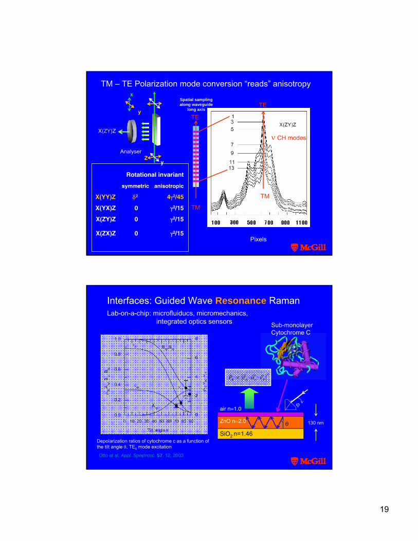
X(ZY)Z
yZ
y
x
Analyser
TM – TE Polarization mode conversion “reads” anisotropy
Pixels
ν CH modes
TE
TM
Spatial samplingalong waveguide
long axis
TE
TM
Rotational invariant
symmetric anisotropic
X(YY)Z δ2 4γ2/45
X(YX)Z 0 γ2/15
X(ZY)Z 0 γ2/15
X(ZX)Z 0 γ2/15
Interfaces: Guided Wave Resonance Raman
Otto et al, Appl. Spectrosc. 57, 12, 2003
Lab-on-a-chip: microfluiducs, micromechanics, integrated optics sensors Sub-monolayer
Cytochrome C
Depolarization ratios of cytochrome c as a function of the tilt angle θ, TE0 mode excitation
2ˆˆ PAK eeP ′⋅′⋅′∝ να
θ
air n=1.0
ZnO n=2.0
ϕ
SiO2 n=1.46
130 nm
20
θ
ϕ
B-A+
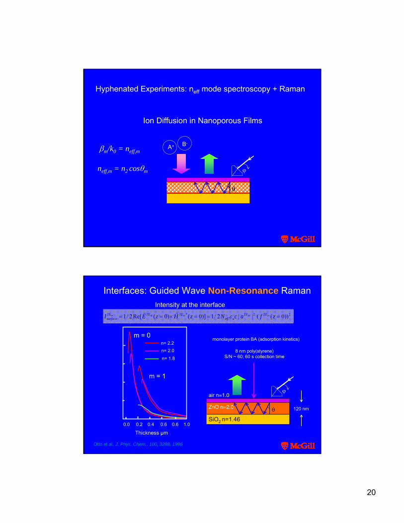
Ion Diffusion in Nanoporous Films
Hyphenated Experiments: neff mode spectroscopy + Raman
βm/k0 = neff,m
neff,m = n2 cosθm
Interfaces: Guided Wave Non-Resonance Raman
Otto et al, J. Phys. Chem., 100, 3288, 1996
22* ))0((||2/1)]0()0(Re[2/1 ===×== zfacNzHzEI mmmmm TETEoeff
TETETEsurface ε
Intensity at the interface
m = 0
m = 1
Thickness µm0.0 0.2 0.4 0.6 0.6 1.0
n= 2.2n= 2.0
n= 1.88 nm poly(styrene)
S/N ~ 60; 60 s collection time
θ
air n=1.0
ZnO n=2.0
ϕ
SiO2 n=1.46
120 nm
monolayer protein BA (adsorption kinetics)
21
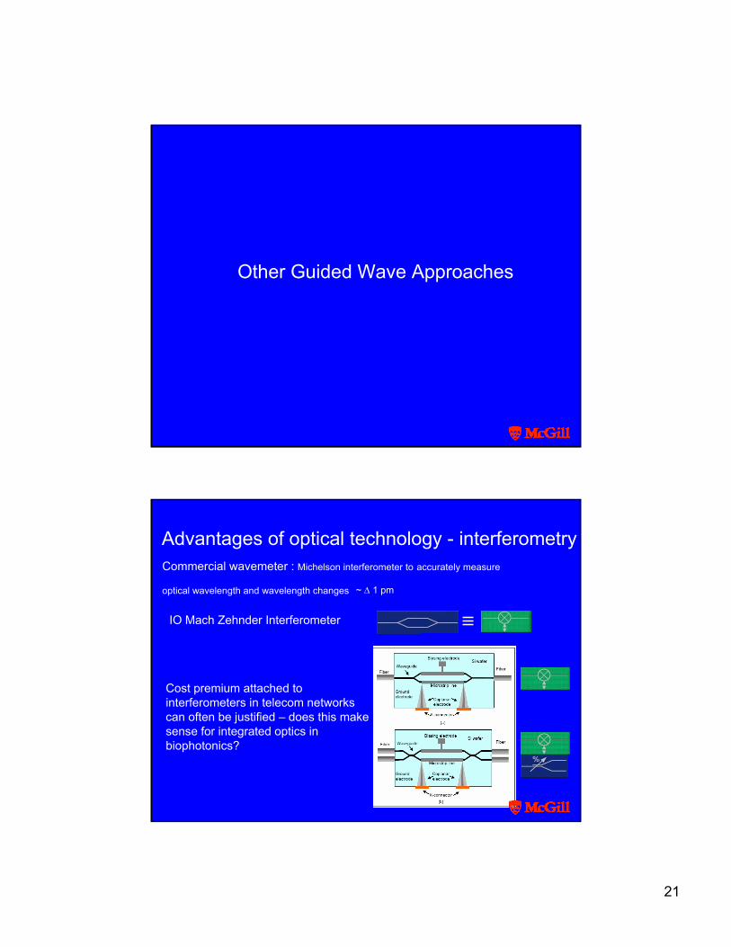
Other Guided Wave Approaches
Advantages of optical technology - interferometryCommercial wavemeter : Michelson interferometer to accurately measure
optical wavelength and wavelength changes ~ Δ 1 pm
IO Mach Zehnder Interferometer
Cost premium attached to interferometers in telecom networks can often be justified – does this make sense for integrated optics in biophotonics?
22
Farfield INFO
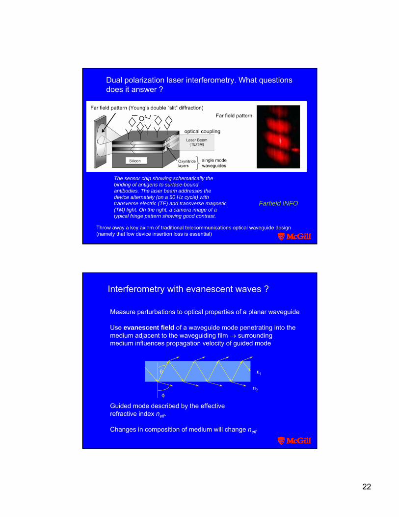
Dual polarization laser interferometry. What questionsdoes it answer ?
The sensor chip showing schematically the binding of antigens to surface-boundantibodies. The laser beam addresses the device alternately (on a 50 Hz cycle) with transverse electric (TE) and transverse magnetic (TM) light. On the right, a camera image of a typical fringe pattern showing good contrast.
Far field pattern
optical coupling
single modewaveguides
Throw away a key axiom of traditional telecommunications optical waveguide design (namely that low device insertion loss is essential)
Far field pattern (Young’s double “slit” diffraction)
Measure perturbations to optical properties of a planar waveguide
Use evanescent field of a waveguide mode penetrating into the medium adjacent to the waveguiding film → surroundingmedium influences propagation velocity of guided mode
Guided mode described by the effectiverefractive index neff.
Changes in composition of medium will change neff
n2
n1
φ
θ
Interferometry with evanescent waves ?
23
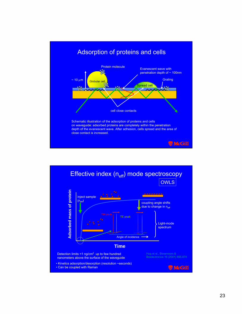
Globular cell
Protein moleculeEvanescent wave withpenetration depth of ~ 100nm
Spread cell
cell close contacts
~ 10 μm
Schematic illustration of the adsorption of proteins and cellson waveguide: adsorbed proteins are completely within the penetrationdepth of the evanescent wave. After adhesion, cells spread and the area of close contact is increased.
Adsorption of proteins and cells
Grating
Effective index (neff) mode spectroscopy
• Kinetics adsorption/desorption (resolution ~seconds)• Can be coupled with Raman
Detection limits <1 ng/cm2 up to few hundred nanometers above the surface of the waveguide
Time
Ads
orbe
d m
ass
of p
rote
in
inject sample(neff) coupling angle shifts
due to change in neff
Light-mode spectrum
TM peakTE peak
Angle of incidence
OWLS
Hug et al., Biosensors & Bioelectronics 16 (2001) 865.874
24
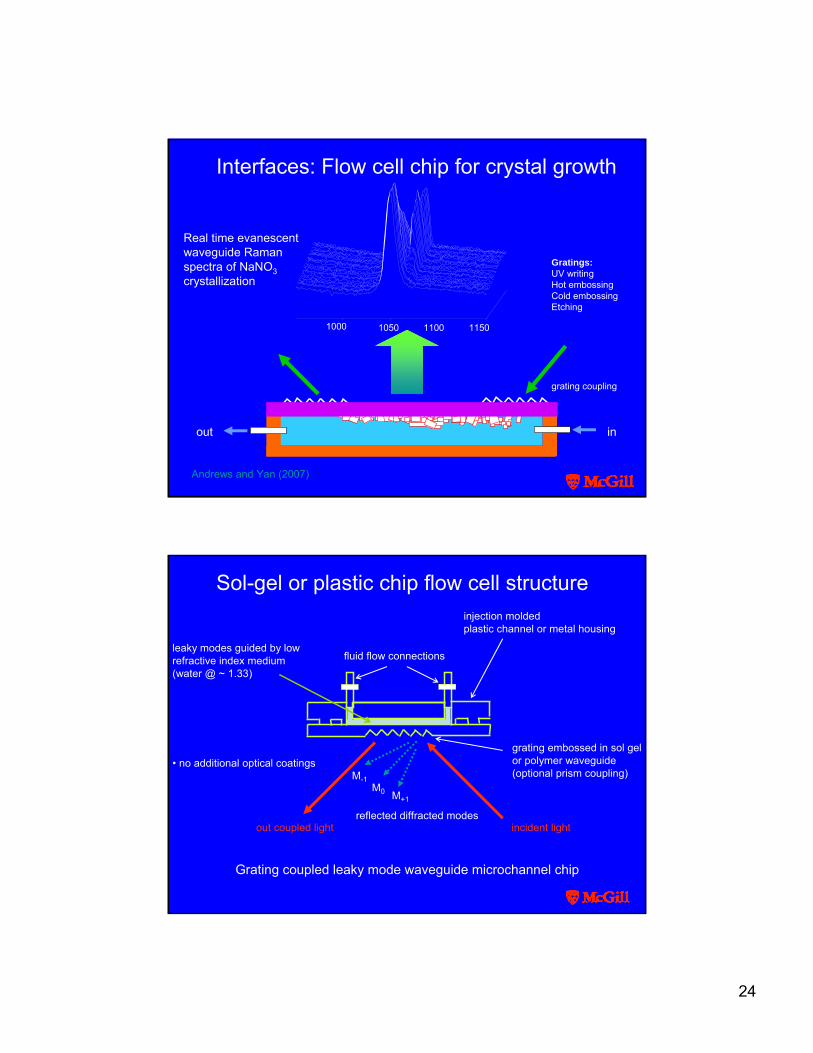
Interfaces: Flow cell chip for crystal growth
inout
grating coupling
Real time evanescent waveguide Raman spectra of NaNO3crystallization
1000 1050 1100 1150
Gratings:UV writingHot embossingCold embossingEtching
Andrews and Yan (2007)
injection moldedplastic channel or metal housing
grating embossed in sol gelor polymer waveguide(optional prism coupling)
reflected diffracted modes
M-1M0 M+1
out coupled light incident light
fluid flow connections
Sol-gel or plastic chip flow cell structure
Grating coupled leaky mode waveguide microchannel chip
leaky modes guided by low refractive index medium (water @ ~ 1.33)
• no additional optical coatings
25
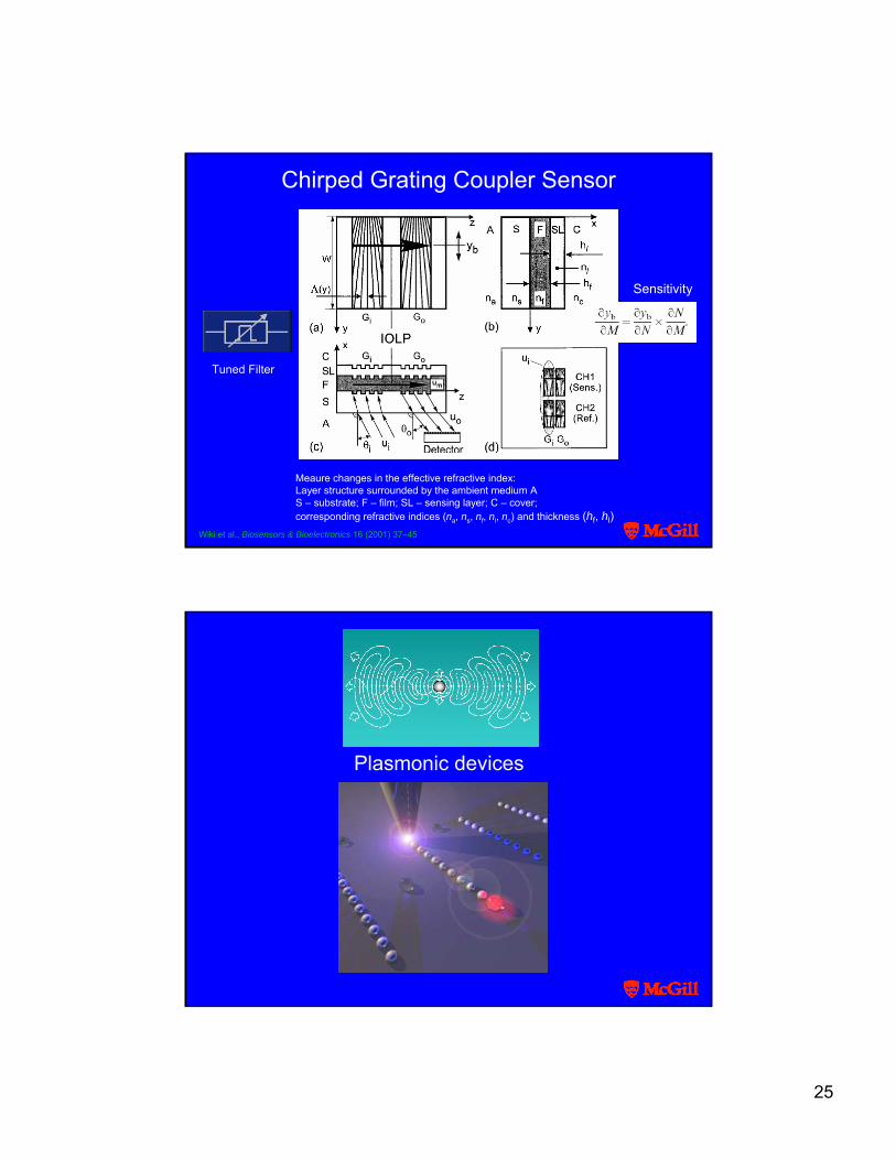
Meaure changes in the effective refractive index: Layer structure surrounded by the ambient medium A S – substrate; F – film; SL – sensing layer; C – cover; corresponding refractive indices (na, ns, nf, nl, nc) and thickness (hf, hl)
Chirped Grating Coupler Sensor
Tuned Filter
Sensitivity
Wiki et al., Biosensors & Bioelectronics 16 (2001) 37–45
Plasmonic devices
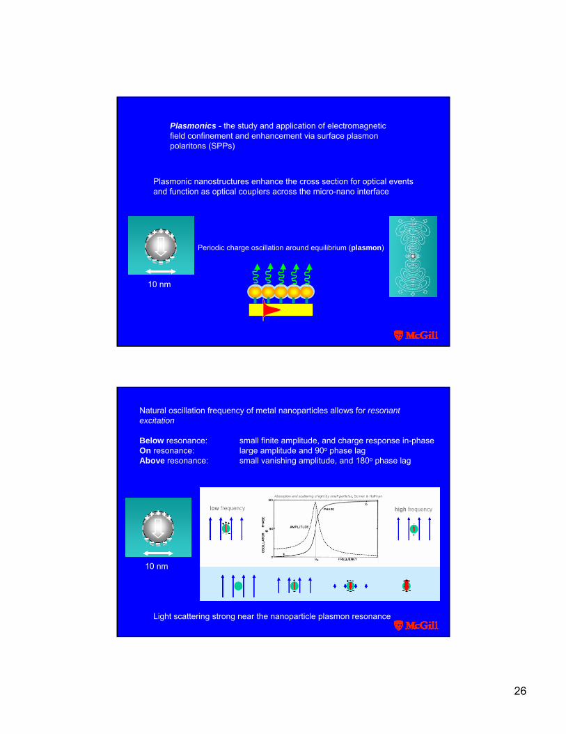
26
10 nm
Periodic charge oscillation around equilibrium (plasmon)
Plasmonic nanostructures enhance the cross section for optical events and function as optical couplers across the micro-nano interface
Plasmonics - the study and application of electromagnetic field confinement and enhancement via surface plasmonpolaritons (SPPs)
Natural oscillation frequency of metal nanoparticles allows for resonant excitation
Below resonance: small finite amplitude, and charge response in-phaseOn resonance: large amplitude and 90o phase lagAbove resonance: small vanishing amplitude, and 180o phase lag
10 nm
Light scattering strong near the nanoparticle plasmon resonance
27
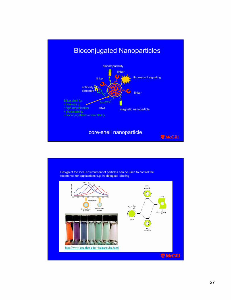
Bioconjugated Nanoparticles
core-shell nanoparticle
Silica shell for:• bioimaging• high amplification• photostability• bioconjugation/biocomptibility
magnetic nanoparticle
linker
linker
linker fluorescent signaling
biocompatibility
antibodydetection
DNA
Design of the local environment of particles can be used to control the resonance for applications e.g. in biological labeling
28
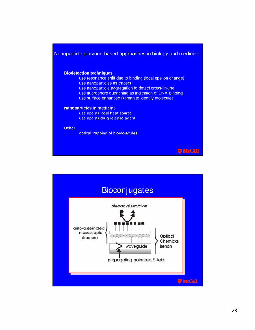
Biodetection techniquesuse resonance shift due to binding (local epsilon change)use nanoparticles as tracersuse nanoparticle aggregation to detect cross-linkinguse fluorophore quenching as indication of DNA bindinguse surface enhanced Raman to identify molecules
Nanoparticles in medicineuse nps as local heat sourceuse nps as drug release agent
Otheroptical trapping of biomolecules
Nanoparticle plasmon-based approaches in biology and medicine
a dhesive benchn anopartic le opticaf ield inten sifier laym olecular adhesivewave guide
=
ω
2 ω Ag surfaceCS
NCH 3(CH2)17CH NHO ONCH3 (CH)21
Sχ= 4 x 1 0 es u(2) -8
D AASP
interfacial reaction
OpticalChemical Benchwaveguide
propagating polarized E-field
mesoscopic structure
auto-assembled
interfacial reaction
OpticalChemical Benchwaveguide
propagating polarized E-field
mesoscopic structure
auto-assembled
Bioconjugates
29
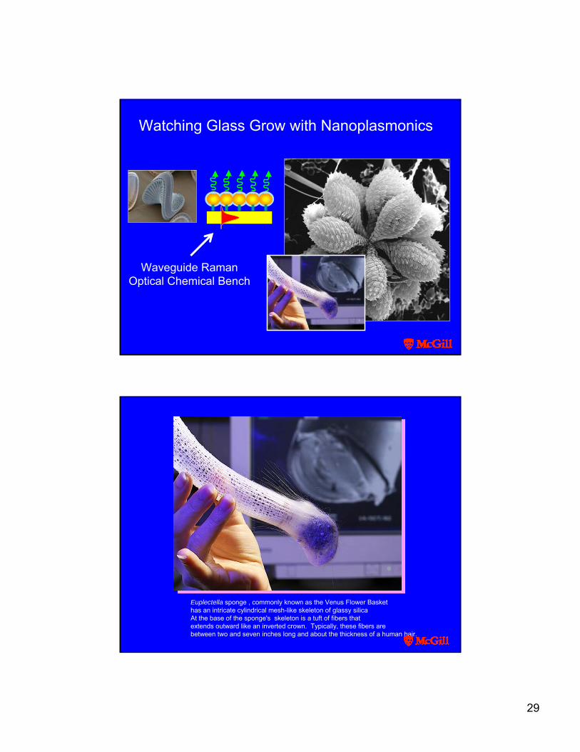
Watching Glass Grow with Nanoplasmonics
Waveguide RamanOptical Chemical Bench
Euplectella sponge , commonly known as the Venus Flower Baskethas an intricate cylindrical mesh-like skeleton of glassy silica At the base of the sponge's skeleton is a tuft of fibers that extends outward like an inverted crown. Typically, these fibers are between two and seven inches long and about the thickness of a human hair.
30
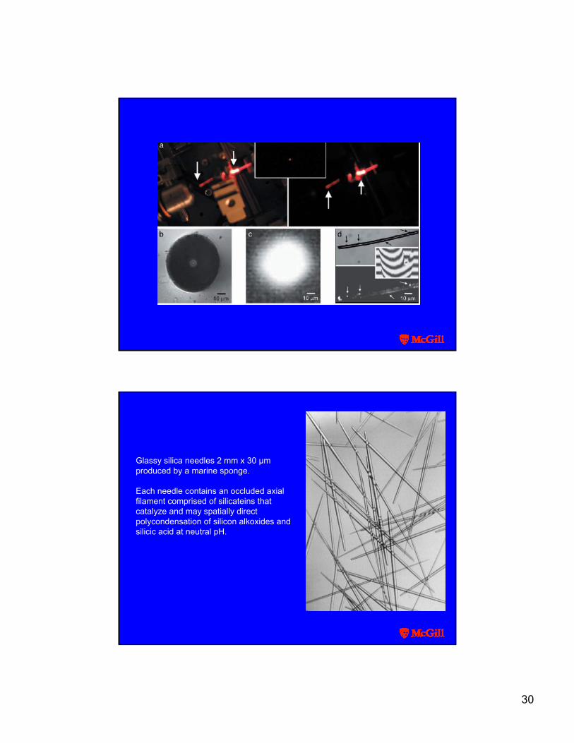
Glassy silica needles 2 mm x 30 µm produced by a marine sponge.
Each needle contains an occluded axial filament comprised of silicateins that catalyze and may spatially direct polycondensation of silicon alkoxides and silicic acid at neutral pH.
31
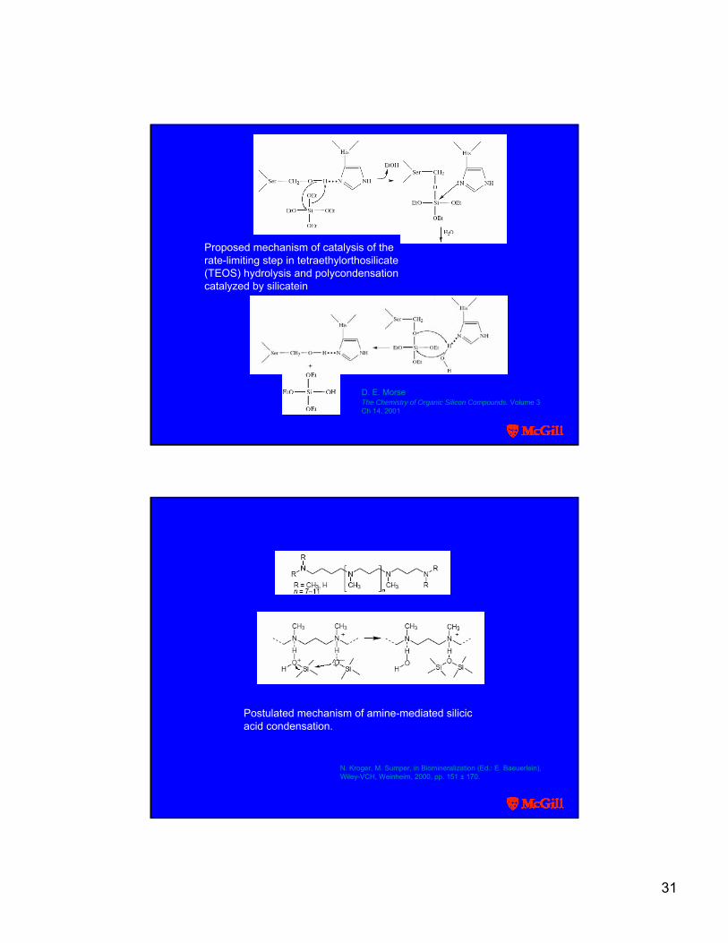
Proposed mechanism of catalysis of the rate-limiting step in tetraethylorthosilicate(TEOS) hydrolysis and polycondensationcatalyzed by silicatein
The Chemistry of Organic Silicon Compounds. Volume 3Ch 14, 2001
D. E. Morse
Postulated mechanism of amine-mediated silicicacid condensation.
N. Kroger, M. Sumper, in Biomineralization (Ed.: E. Baeuerlein),Wiley-VCH, Weinheim, 2000, pp. 151 ± 170.
32
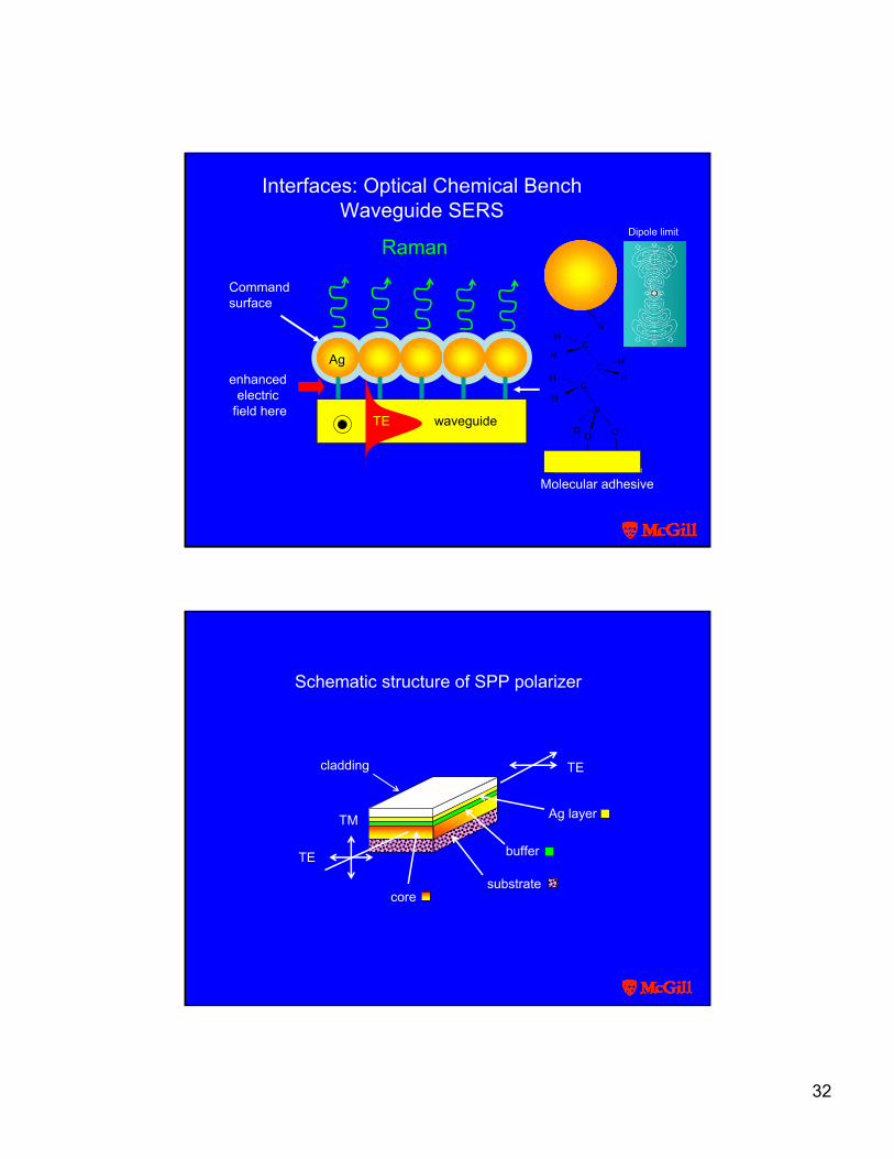
Commandsurface
Raman
enhanced electric
field herewaveguide
Ag
TE
Interfaces: Optical Chemical BenchWaveguide SERS
Dipole limit
Molecular adhesive
Si
C
C
C
S
OO
H
H
H
H
H
H
O
Schematic structure of SPP polarizer
cladding
TM
TE
TE
Ag layer
buffer
coresubstrate
33
n= 1.5125
1 μm
n= 1.6150Ag
n= 1.4400
50 nm
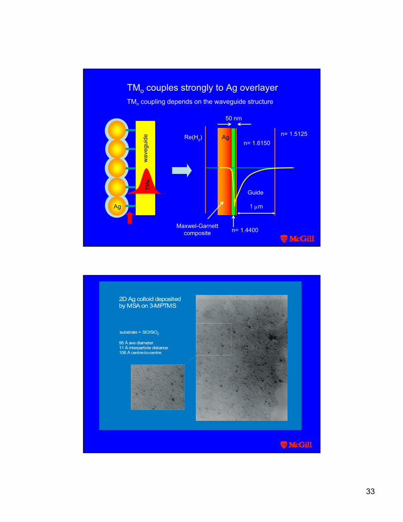
TMo couples strongly to Ag overlayer
Re(Hy)
Guide
wav
egui
de
Ag
TMo
Maxwel-Garnettcomposite
TMn coupling depends on the waveguide structure
2D Ag colloid deposited by MSA on 3-MPTMS
substrate = SiO/SiO2
95 Å ave diameter11 Å interparticle distance106 Å centre-to-centre
34
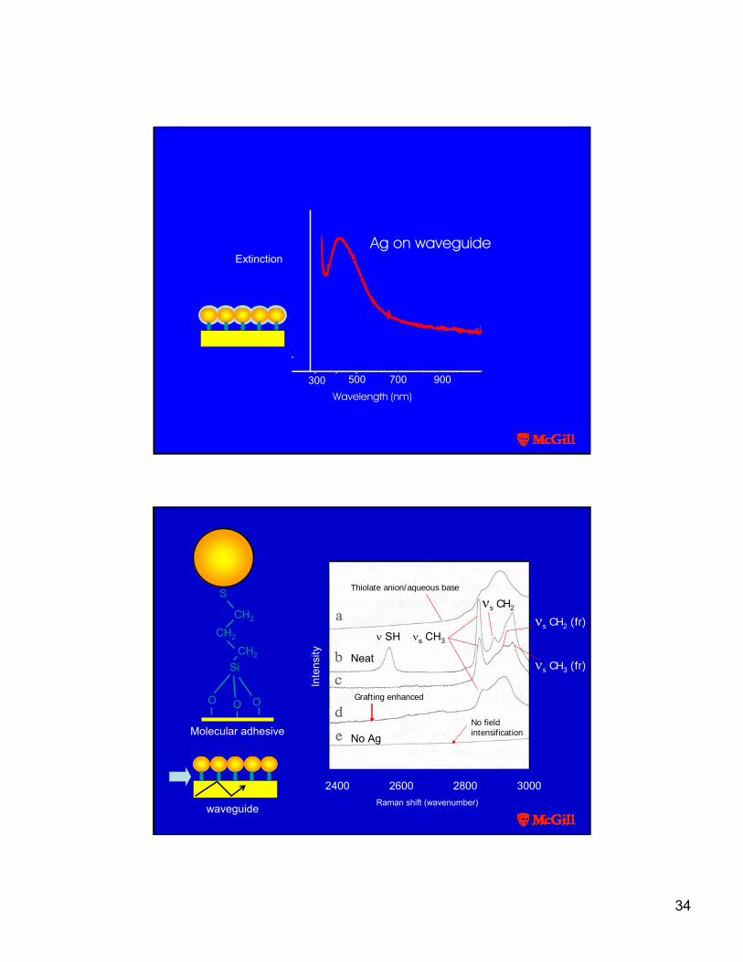
300 500 700 900 Wavelength (nm)
Absorbance (arbitrary units)
Ag on waveguideExtinction
νs CH3
waveguide
Neat
ν SH
2400 2600 2800 3000Raman shift (wavenumber)
Inte
nsity
No Ag
CH2
CH2
CH2
S
Si
O O O
Molecular adhesive
Grafting enhanced
No fieldintensification
νs CH2
νs CH2 (fr)
νs CH3 (fr)
Thiolate anion/aqueous base
35
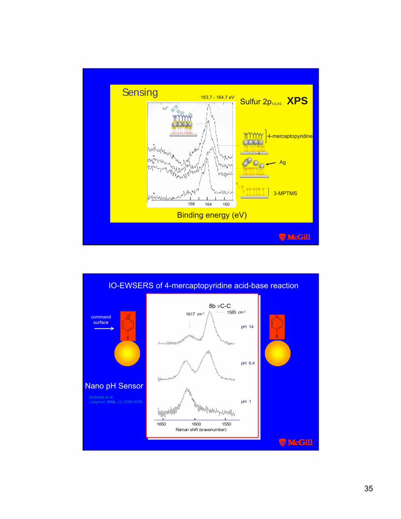
163.7 - 164.7 eV
Cu2+
4-mercaptopyridine
Ag
SH SH SH SH SH
SH
SH
3-MPTMS
Sulfur 2p XPS1/2,3/2
164 160168
Binding energy (eV)
Sensing
1650 1600 1550
IO-EWSERS of 4-MPy titrated by acid/base
pH 1
pH 6.4
pH 14
1617 1585
Raman shift (wavenumber)
cm-1 cm-1
N
S
N
S
H+
IO-EWSERS of 4-mercaptopyridine acid-base reaction
Nano pH SensorAndrews et al.Langmuir 1996, 12, 6389-6398
8b νC-C
commandsurface
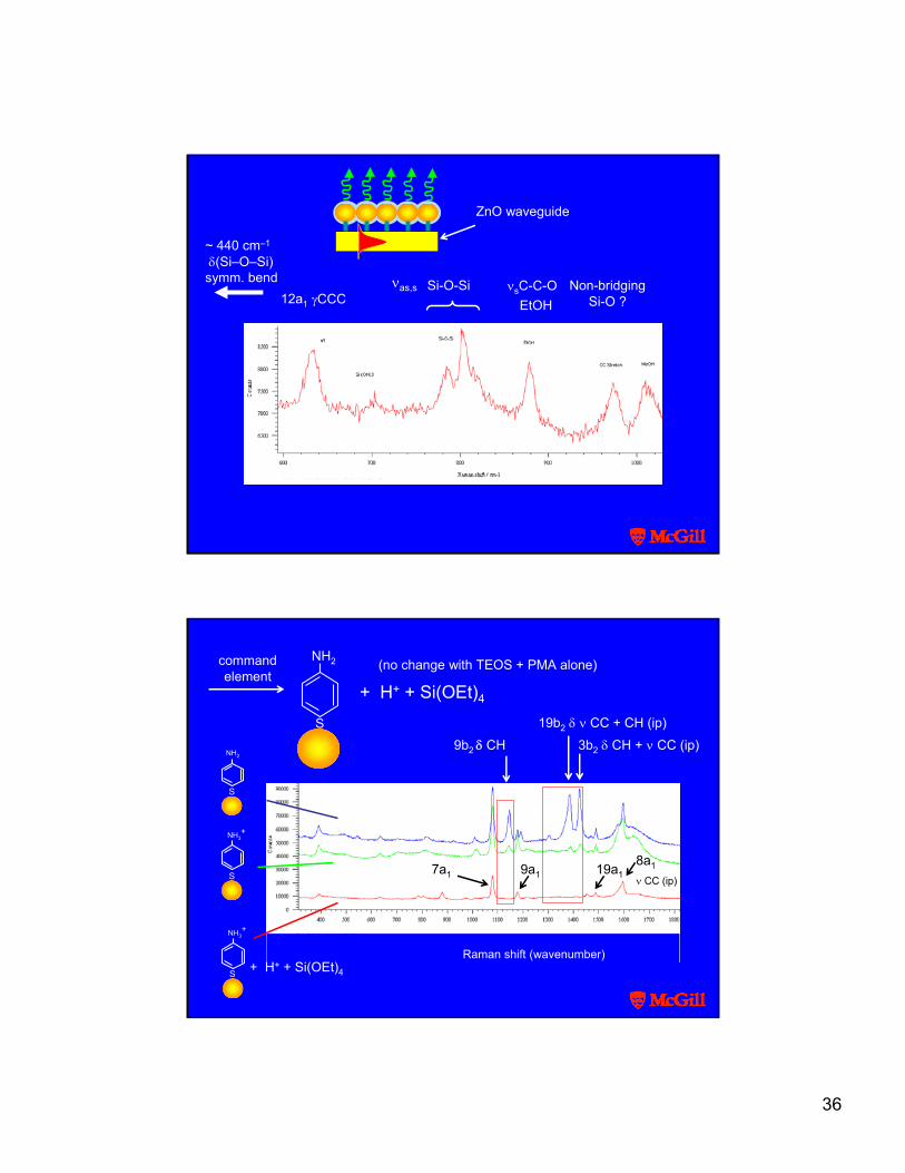
36
γCCC 12a1
Si-O-Si EtOH
νsC-C-O
~ 440 cm–1
δ(Si–O–Si)symm. bend νas,s Non-bridging
Si-O ?
ZnO waveguide
Si(OH)
656 cm-1D
Raman shift (wavenumber)
S
NH2
+ H+ + Si(OEt)4
S
NH2
S
NH3+
S
NH3+
+ H+ + Si(OEt)4
(no change with TEOS + PMA alone)
7a1 9a1 19a18a1
commandelement
19b2 δ ν CC + CH (ip)
ν CC (ip)
3b2 δ CH + ν CC (ip) 9b2 δ CH
37
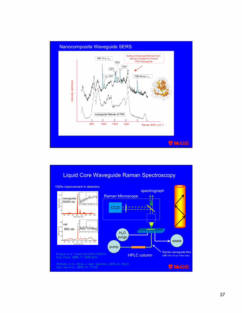
1596 8a (a ) 1 ccν
999 12 a 1 ccβ
1221
1231
1301
βCH 1027
Raman Shift ( cm )-112001000800 1400
waveguide Raman of PVA
Benzyl thiolate/Au FractalPVA Waveguide
Surface Enhanced Raman from
Inte
nsity
(arb
itrar
y)
S
SS
S
SS
S
S S
SS
SS
S S
S
SS
S
S
SSS
S
S
S
S
S
S
SS
SS
S
S
S S
S
SSS
S
S
SS
S
S
S
S
SS
S
S
S
SS
SS S
S S
S
SS
S
S
SS
S
S
S
S
S
SS
S
S
Nanocomposite Waveguide SERS
Liquid Core Waveguide Raman Spectroscopy
Burgess et al. Talanta 59 (2003) 809/816Anal. Chem. 1999, 71, 4808-4814
Walfaren, G. E.; Stone, J. Appl. Spectrosc. 1972, 26, 585-9;Appl. Spectrosc. 1975, 29, 179-85.
spectrograph
CCD
HPLC column
H2Opurge
waste
Raman Microscope
Raman waveguide flowcell (1M x 50 µm Teflon tube)
pump
waveguide50000 cts
vial
800 cts
1000x improvement in detection
38
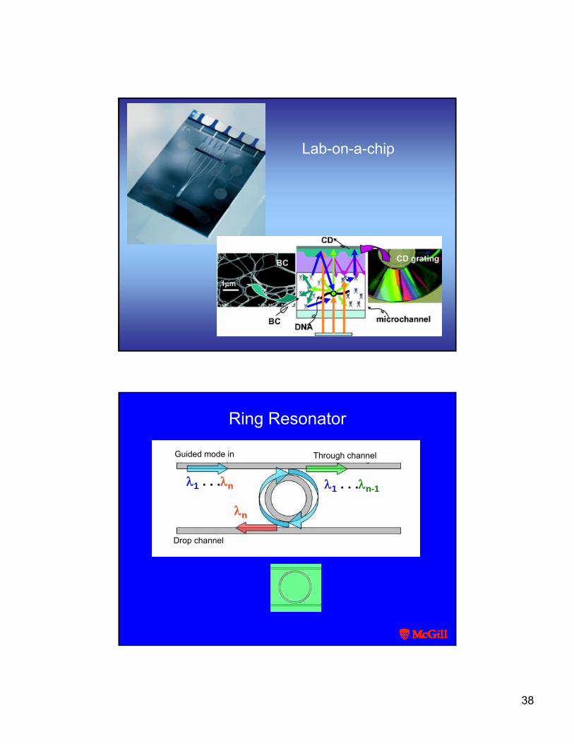
Lab-on-a-chip
Ring Resonator
λ1 . . .λn λ1 . . .λn-1
λn
Guided mode in Through channel
Drop channel
39
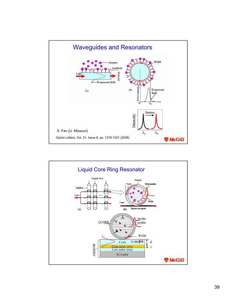
Waveguides and Resonators
X. Fan (U. Missouri)
Optics Letters, Vol. 31, Issue 9, pp. 1319-1321 (2006)
Liquid Core Ring Resonator
40
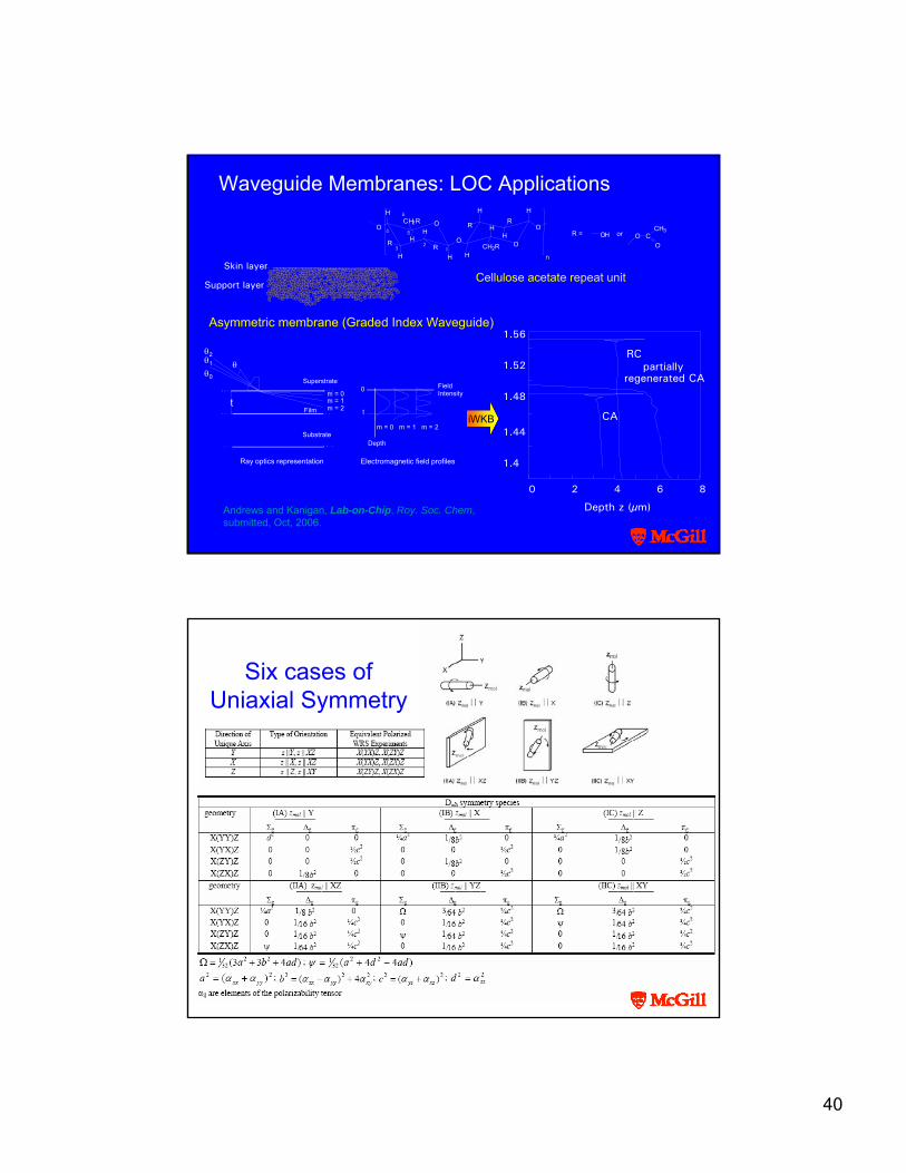
Skin layer
Support layer
Asymmetric membrane (Graded Index Waveguide)
Depth z (µm)
Refractive Index n
1.4
1.44
1.48
1.52
1.56
0 2 4 6 8
CA
partiallyregenerated CA
RC
Ray optics representation Electromagnetic field profiles
Substrate
Film
Superstrate
Depth
Field Intensitym = 0
m = 1m = 2
m = 0 m = 1 m = 2
0
t
θθ1
t
θ2
θ0
Waveguide Membranes: LOC Applications
iWKB
Andrews and Kanigan, Lab-on-Chip, Roy. Soc. Chem,submitted, Oct, 2006.
n1
2
4
6
3
5O
H
O
R
H
HH
CH2R
HR
O
O
H
CH2RH
H
H
R
H
O
R
O CO
CH3OHR = or
Cellulose acetate repeat unit
Six cases ofUniaxial Symmetry
41
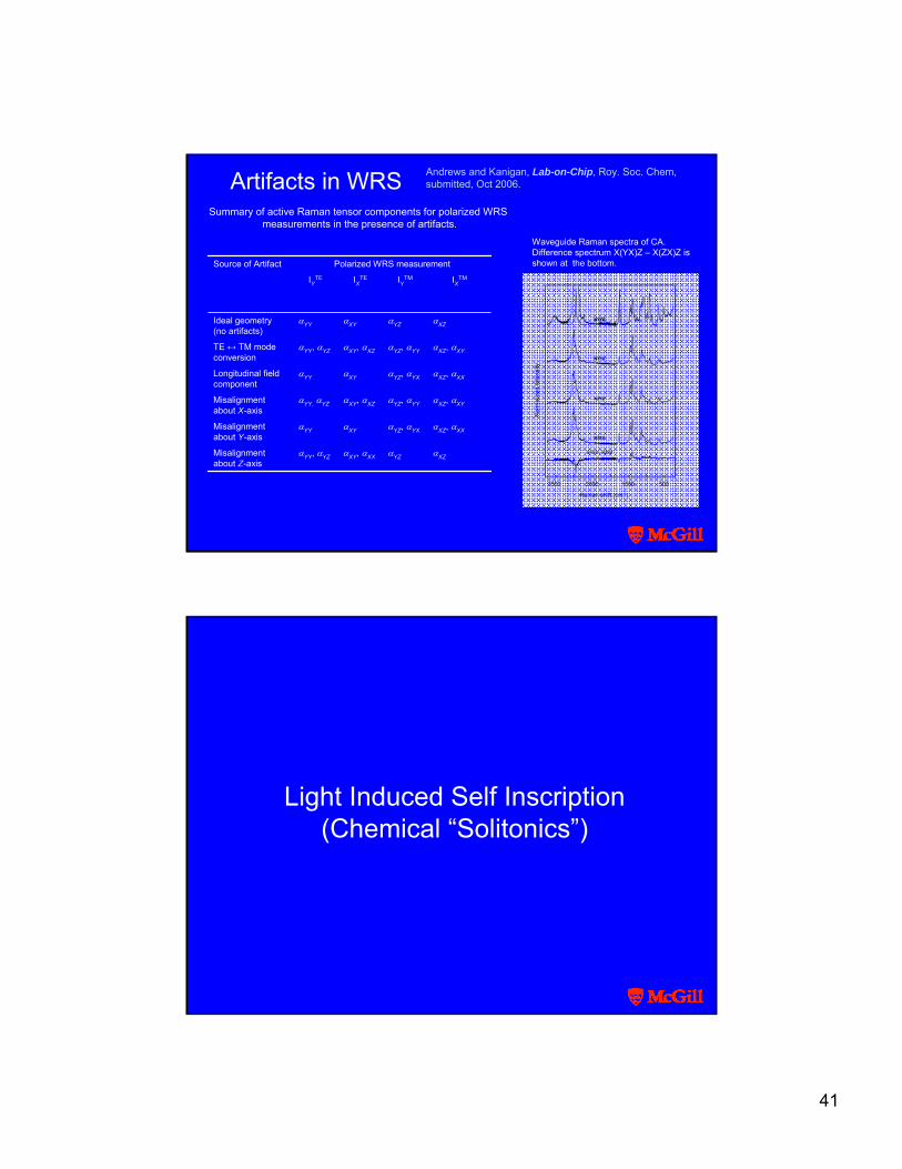
Summary of active Raman tensor components for polarized WRS measurements in the presence of artifacts.
αXZαYZαXY, αXXαYY, αYZMisalignment about Z-axis
αXZ, αXXαYZ, αYXαXYαYYMisalignment about Y-axis
αXZ, αXYαYZ, αYYαXY, αXZαYY, αYZMisalignment about X-axis
αXZ, αXXαYZ, αYXαXYαYYLongitudinal field component
αXZ, αXYαYZ, αYYαXY, αXZαYY, αYZTE ↔ TM mode conversion
αXZαYZαXYαYYIdeal geometry(no artifacts)
IXTMIYTMIXTEIYTE
Polarized WRS measurementSource of Artifact
Waveguide Raman spectra of CA. Difference spectrum X(YX)Z – X(ZX)Z is shown at the bottom.
Artifacts in WRS Andrews and Kanigan, Lab-on-Chip, Roy. Soc. Chem,submitted, Oct 2006.
Light Induced Self Inscription(Chemical “Solitonics”)
42
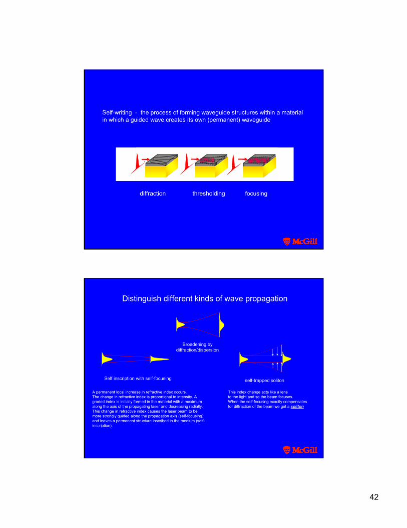
Self-writing - the process of forming waveguide structures within a materialin which a guided wave creates its own (permanent) waveguide
diffraction thresholding focusing
Broadening bydiffraction/dispersion
Self inscription with self-focusing self-trapped soliton
Distinguish different kinds of wave propagation
This index change acts like a lens to the light and so the beam focuses. When the self-focusing exactly compensates for diffraction of the beam we get a soliton
A permanent local increase in refractive index occurs.The change in refractive index is proportional to intensity. A graded index is initially formed in the material with a maximum along the axis of the propagating laser and decreasing radially. This change in refractive index causes the laser beam to be more strongly guided along the propagation axis (self-focusing) and leaves a permanent structure inscribed in the medium (self-inscription).
43
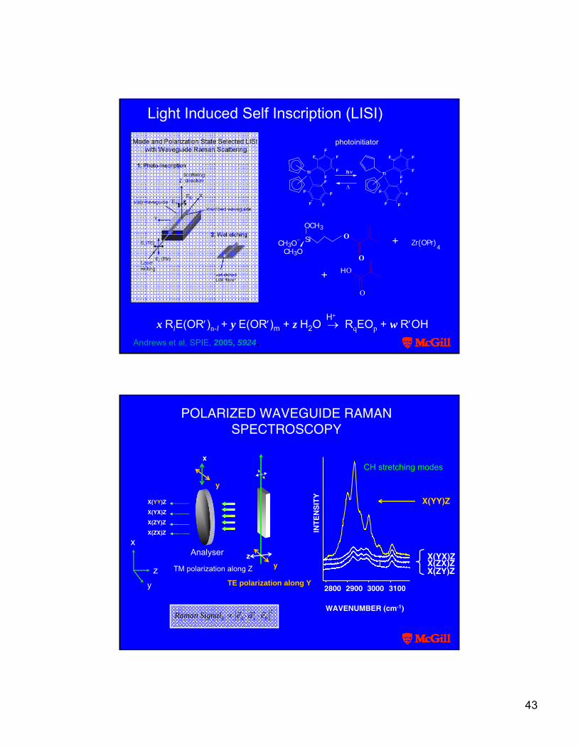
x RlE(OR′)n-l + y E(OR′)m + z H2O → RqEOp + w R′OH
Ti
F
F
FF
F
FF
F
FF
Ti
F
F
FF
F
FF
F
FF
hν
Δ
Si
OCH3
CH3OCH3O
O
O
Zr(OPr)4
O
O
H
+
+
Light Induced Self Inscription (LISI)
photoinitiator
H+
Andrews et al, SPIE, 2005, 5924.
POLARIZED WAVEGUIDE RAMAN SPECTROSCOPY
y
TM polarization along Z
TE polarization along Y
X(YY)Z
X(YX)Z
X(ZY)Z
X(ZX)Z
yz
y
x
Analyser
2800 2900 3000 3100
X(YY)Z
X(ZX)ZX(YX)Z
X(ZY)Z
WAVENUMBER (cm-1)
INT
EN
SIT
Y
CH stretching modes
z
x
2ˆˆ PAK eeSignalRaman ′⋅′⋅′∝ να
44
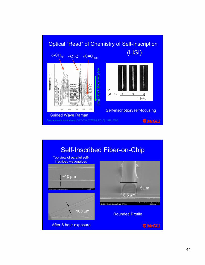
δ-CH ip νC=C νC=O(sat)
Guided Wave RamanSelf-inscription/self-focusing
Saravanamuttu and Andrews, OPTICS LETTERS 27(15), 1342, 2002
Pro
gres
s of
pho
toin
scrip
tion
Optical “Read” of Chemistry of Self-Inscription(LISI)
Self-Inscribed Fiber-on-Chip
After 8 hour exposure
Top view of parallel self-inscribed waveguides
Rounded Profile
~10 μm
~100 μm
~6.5 μm
5 μm
45
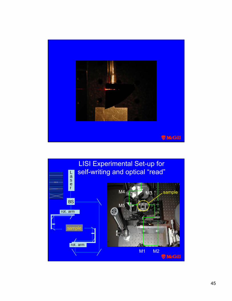
LISI Experimental Set-up forself-writing and optical “read”
sample
rot. arm
Laser
BS
rot. arm
M1 M2
M3M4
M5
sample
46
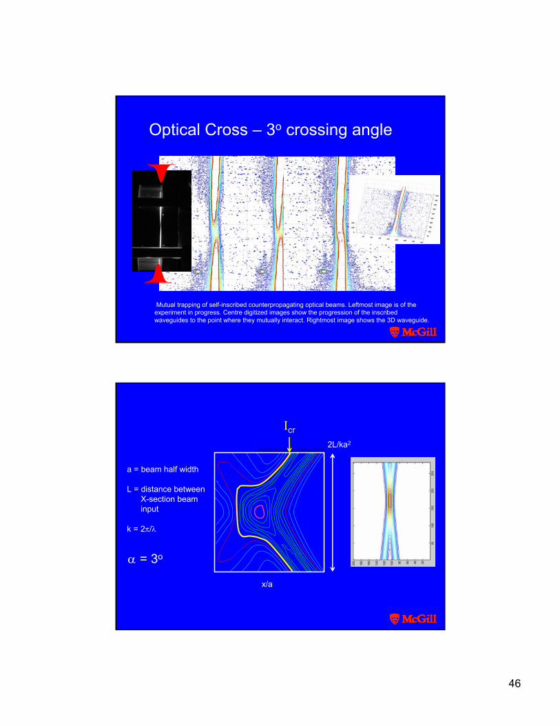
Optical Cross – 3o crossing angle
Mutual trapping of self-inscribed counterpropagating optical beams. Leftmost image is of the experiment in progress. Centre digitized images show the progression of the inscribed waveguides to the point where they mutually interact. Rightmost image shows the 3D waveguide.
α = 3o
a = beam half width
L = distance betweenX-section beaminput
k = 2π/λ
2L/ka2
x/a
Icr
47
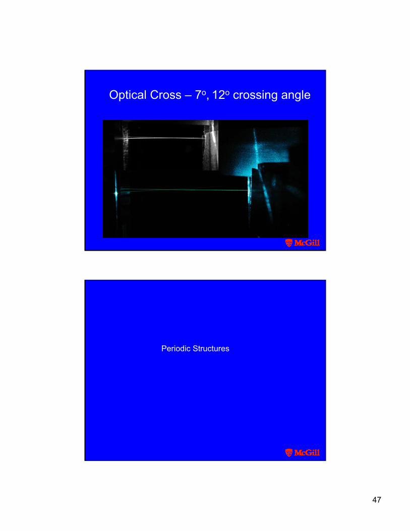
Optical Cross – 7o, 12o crossing angle
Periodic Structures
48
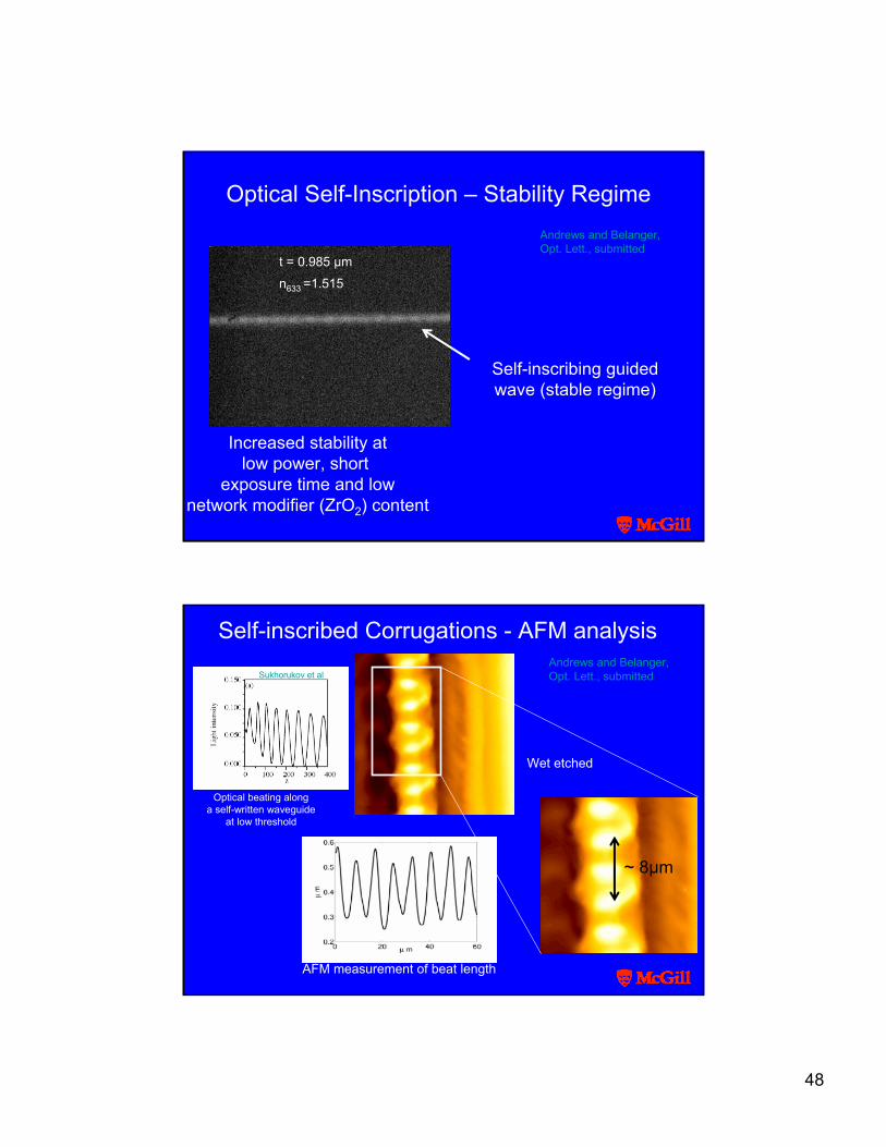
Optical Self-Inscription – Stability Regime
Increased stability atlow power, short
exposure time and lownetwork modifier (ZrO2) content
Self-inscribing guidedwave (stable regime)
t = 0.985 µm
n633 =1.515
Andrews and Belanger,Opt. Lett., submitted
Self-inscribed Corrugations - AFM analysis
~ 8µm
Sukhorukov et al
Optical beating alonga self-written waveguide
at low threshold
AFM measurement of beat length
Andrews and Belanger,Opt. Lett., submitted
Wet etched
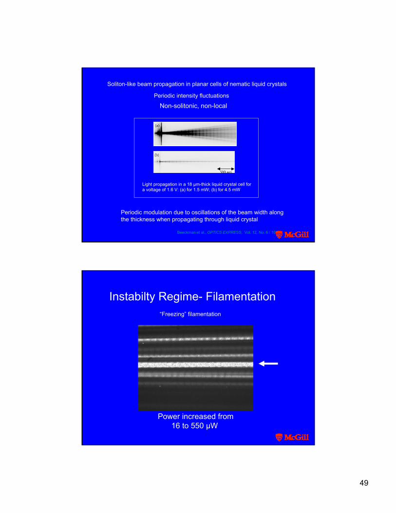
49
Light propagation in a 18 µm-thick liquid crystal cell for a voltage of 1.6 V: (a) for 1.5 mW; (b) for 4.5 mW
Periodic intensity fluctuations
Non-solitonic, non-local
Soliton-like beam propagation in planar cells of nematic liquid crystals
Periodic modulation due to oscillations of the beam width along the thickness when propagating through liquid crystal
Beeckman et al., OPTICS EXPRESS, Vol. 12, No. 6 / 1011
Power increased from16 to 550 µW
Instabilty Regime- Filamentation“Freezing” filamentation
50
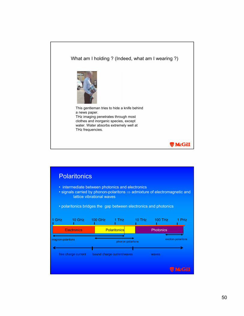
What am I holding ? (Indeed, what am I wearing ?)
This gentleman tries to hide a knife behind a news paper. THz imaging penetrates through most clothes and inorganic species, except water. Water absorbs extremely well at THz frequencies.
Polaritonics• intermediate between photonics and electronics• signals carried by phonon-polaritons ⇒ admixture of electromagnetic and
lattice vibrational waves
• polaritonics bridges the gap between electronics and photonics
1 GHz 10 GHz 100 GHz 1 THz 10 THz 100 THz 1 PHz
Photonics
exciton-polaritonsphonon-polaritons
PolaritonicsElectronics
magnon-polaritons
free charge current bound charge current/waves waves
51
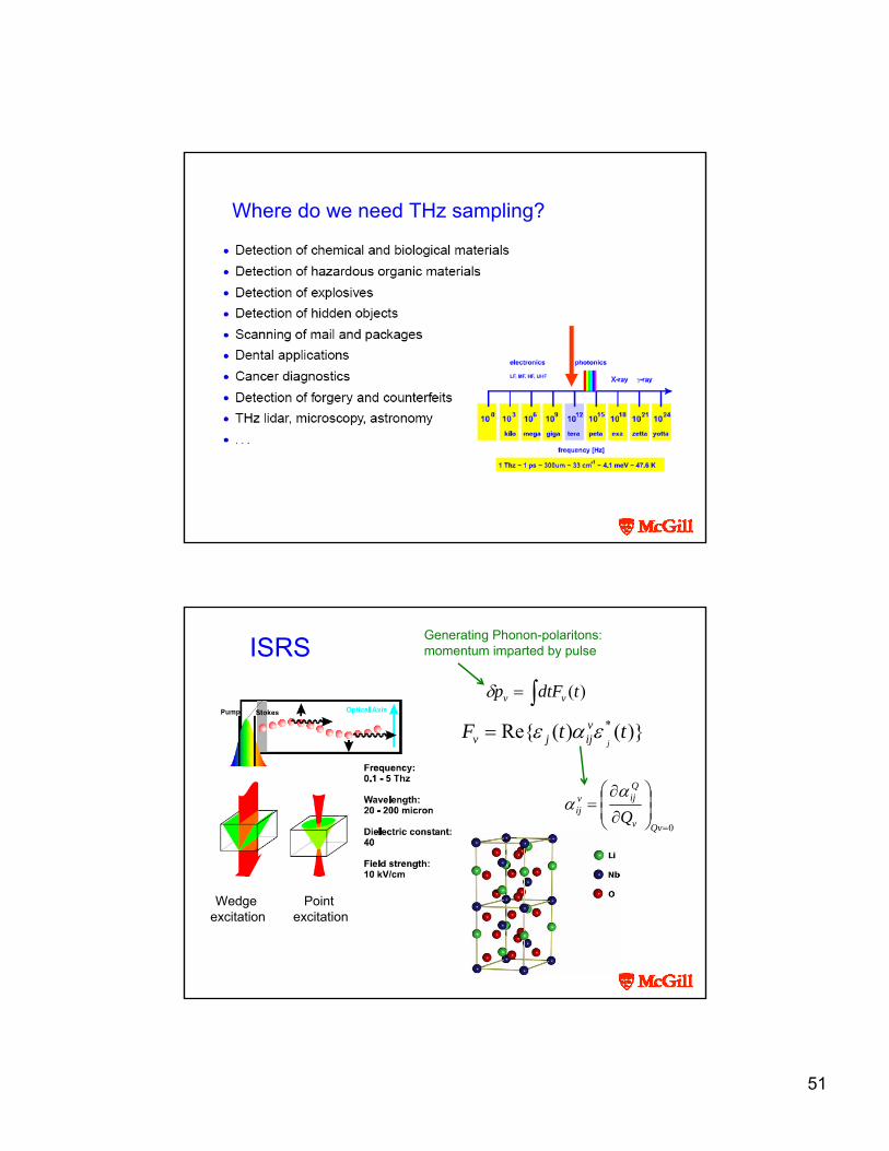
Where do we need THz sampling?
∫= )(tdtFp vvδ
Generating Phonon-polaritons:momentum imparted by pulse
)}()(Re{ * ttFj
vijjv εαε=
0=⎟⎟⎠
⎞⎜⎜⎝
⎛
∂
∂=
Qvv
Qijv
ij Qα
α
ISRS
Wedge excitation
Point excitation
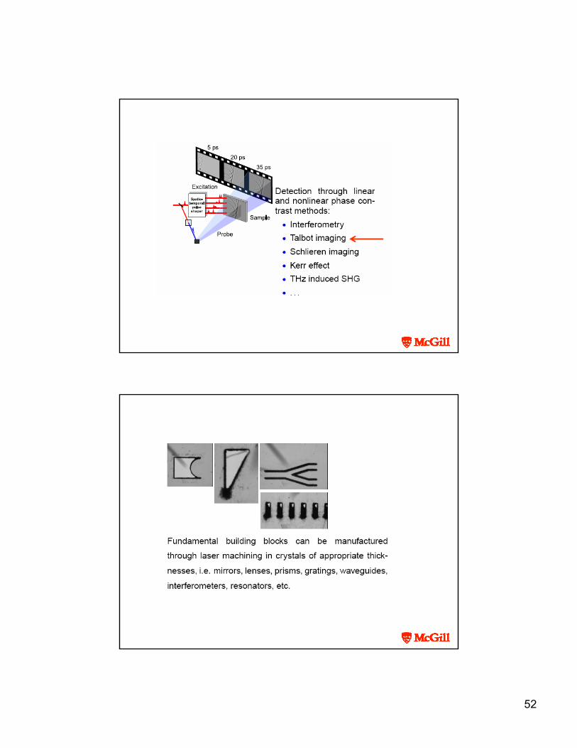
52
53
Polariton field splitting and recombination in a waveguide interferometerin lithium tantalate.
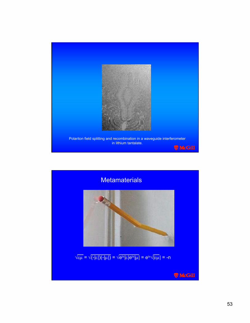
√εμ = √(-|ε|)(-|μ|) = √eiπ|ε|eiπ|μ| = eiπ√|εμ| = -n
Metamaterials
54
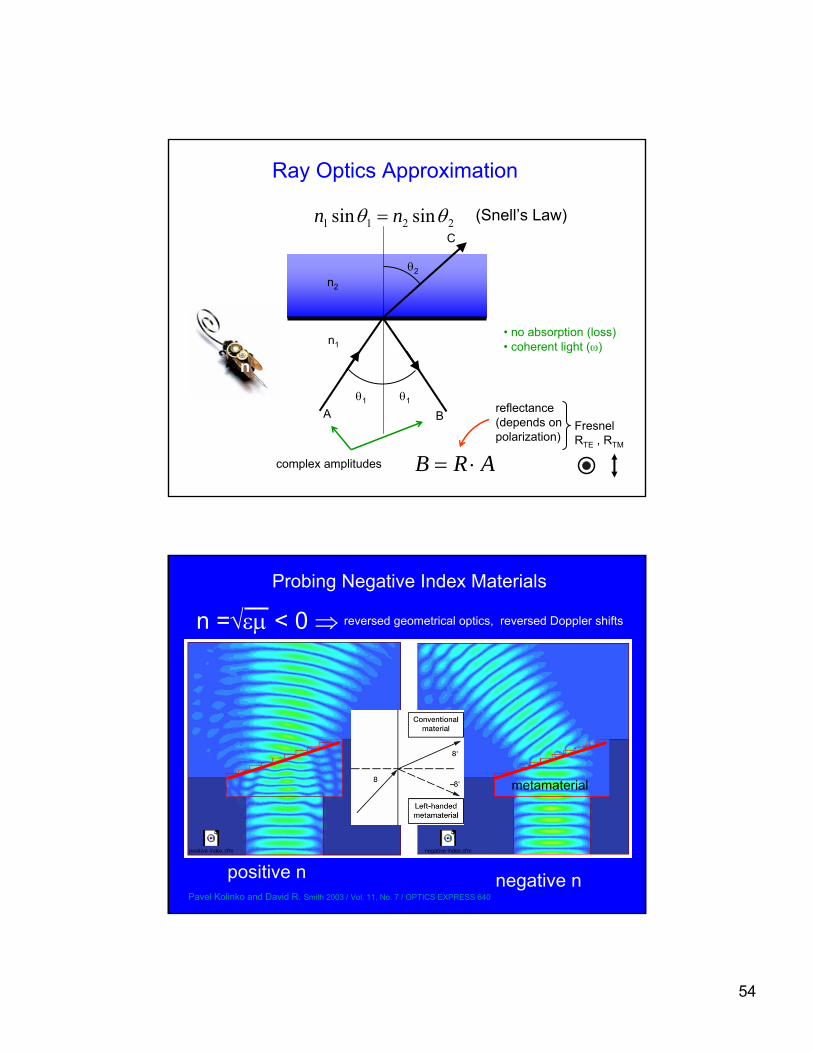
θ2n2
n1
θ1 θ1
A B
C
• no absorption (loss)• coherent light (ω)
2211 sinsin θθ nn = (Snell’s Law)
complex amplitudes ARB ⋅=
reflectance(depends on polarization)
Ray Optics Approximation
n
FresnelRTE , RTM
positive index.cfm negative index.cfm
Probing Negative Index Materials
n =√εμ < 0 ⇒
positive n negative nPavel Kolinko and David R. Smith 2003 / Vol. 11, No. 7 / OPTICS EXPRESS 640
reversed geometrical optics, reversed Doppler shifts
metamaterial
55
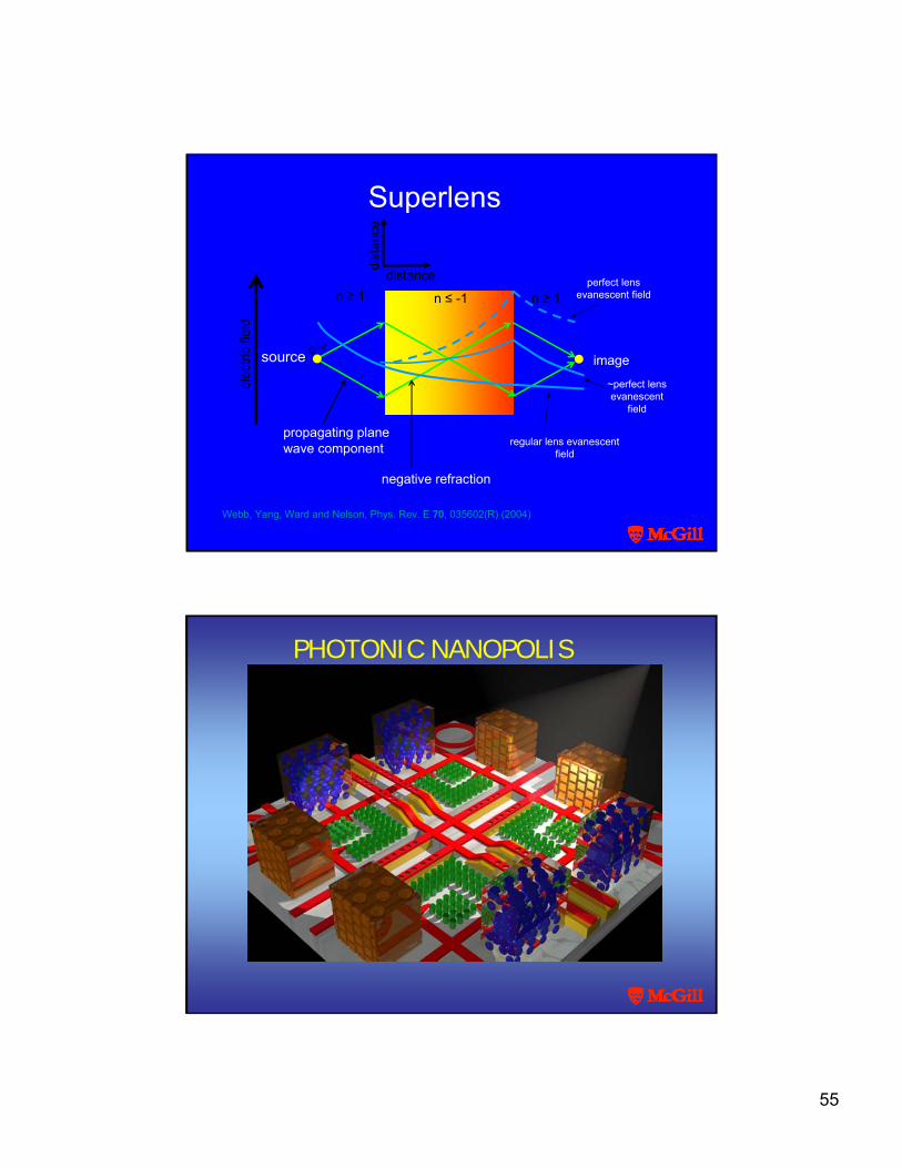
Superlens
source eiωt
n ≥ 1
elec
tric
field
distance
dist
ance
n ≤ -1 n ≥ 1
image
perfect lensevanescent field
~perfect lensevanescent
field
regular lens evanescentfield
propagating planewave component
negative refraction
Webb, Yang, Ward and Nelson, Phys. Rev. E 70, 035602(R) (2004)
PHOTONIC NANOPOLIS
56
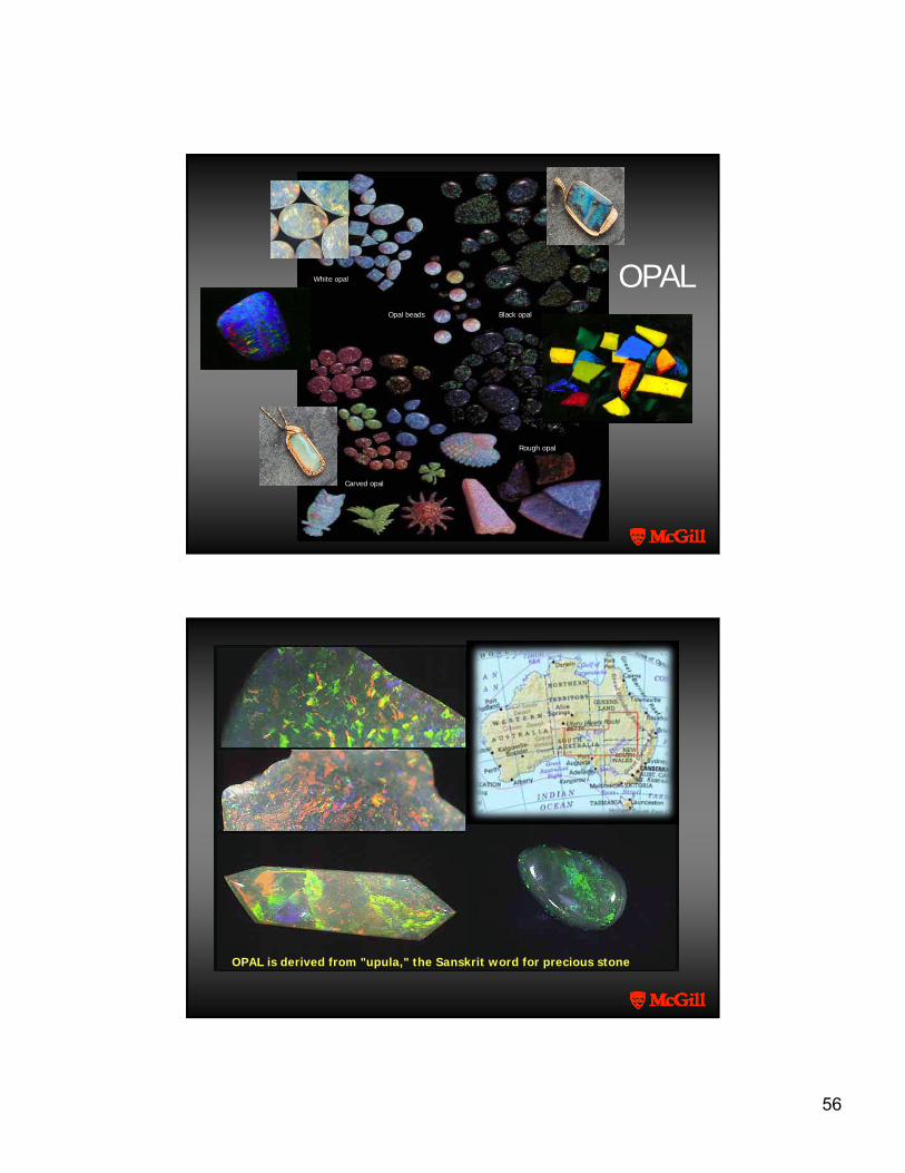
White opal
Opal beads Black opal
Rough opal
Carved opal
OPAL
OPAL is derived from "upula," the Sanskrit word for precious stone
57
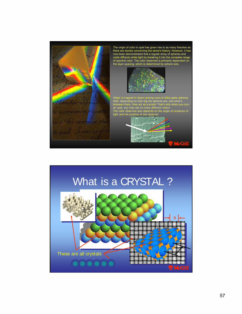
The origin of color in opal has given rise to as many theories as there are stories concerning the stone's history. However, it has now been demonstrated that a regular array of spheres and voids diffracts white light by breaking it into the complete range of spectral color. The color observed is primarily dependent on the layer spacing, which is determined by sphere size.
Water is trapped in layers among rows of silica glass spheres. Well, depending on how big the spheres are, and what's between them, they act as a prism! That's why when you turn an opal, you may see so many different colors.The color observed also depends on the angle of incidence of light and the position of the observer.
What is a CRYSTAL ?
a
These are all crystals
58
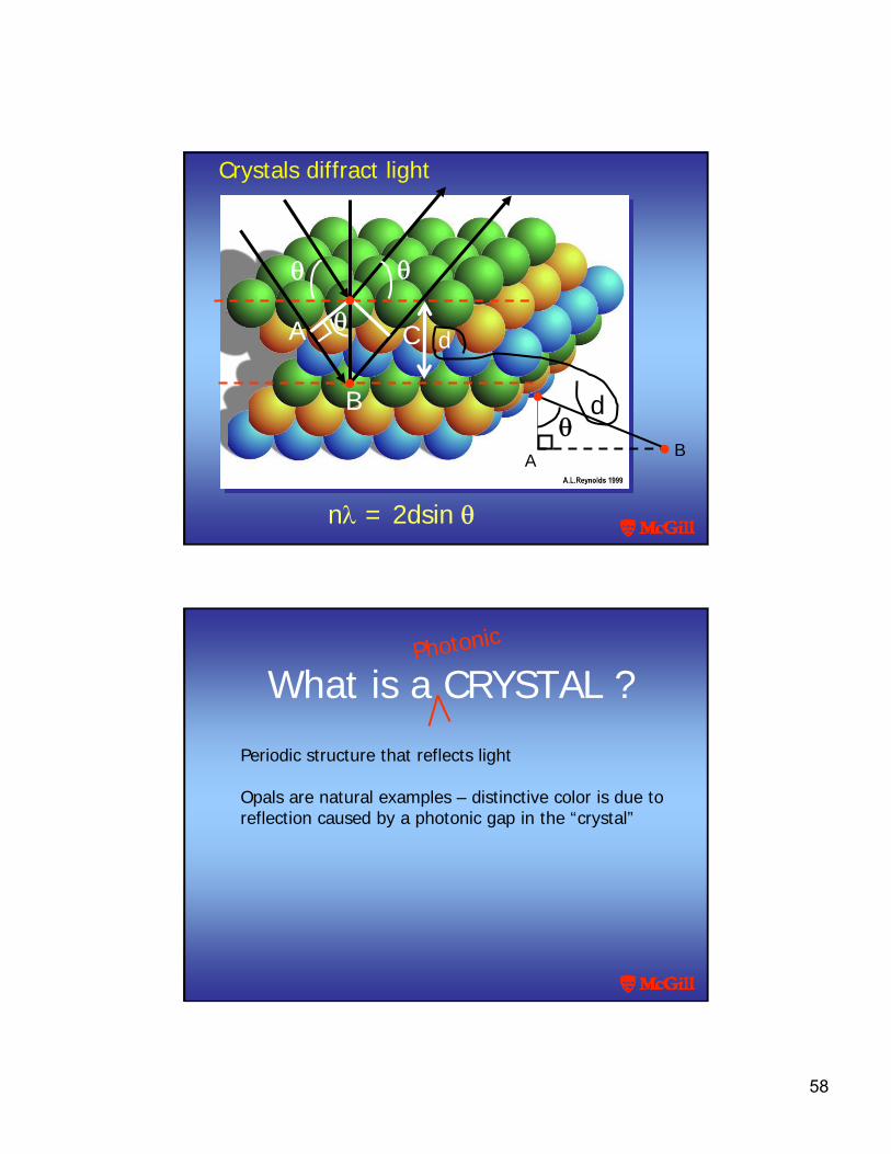
dA
B
C
θθ
θ
A B
dθ
nλ = 2dsin θ
Crystals diffract light
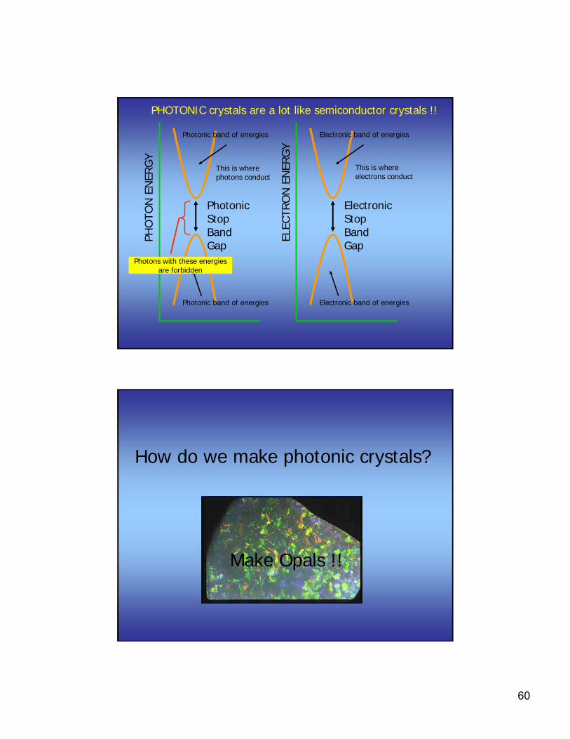
What is a CRYSTAL ?Photonic
Periodic structure that reflects light
Opals are natural examples – distinctive color is due toreflection caused by a photonic gap in the “crystal”
59
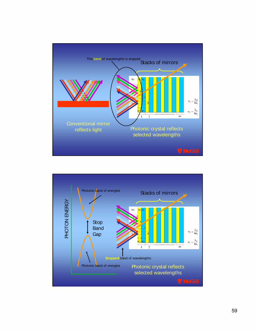
Conventional mirrorreflects light Photonic crystal reflects
selected wavelengths
Stacks of mirrorsThis band of wavelengths is stopped
Photonic crystal reflectsselected wavelengths
Stacks of mirrors
Stopped band of wavelengths
PHO
TON
EN
ERG
Y
StopBand Gap
Photonic band of energies
Photonic band of energies
60
ELEC
TRO
N E
NER
GY
ElectronicStopBand Gap
Electronic band of energies
Electronic band of energies
PHO
TON
EN
ERG
Y
PhotonicStopBand Gap
Photonic band of energies
Photonic band of energies
PHOTONIC crystals are a lot like semiconductor crystals !!
Photons with these energiesare forbidden
This is wherephotons conduct
This is whereelectrons conduct
How do we make photonic crystals?
Make Opals !!
61
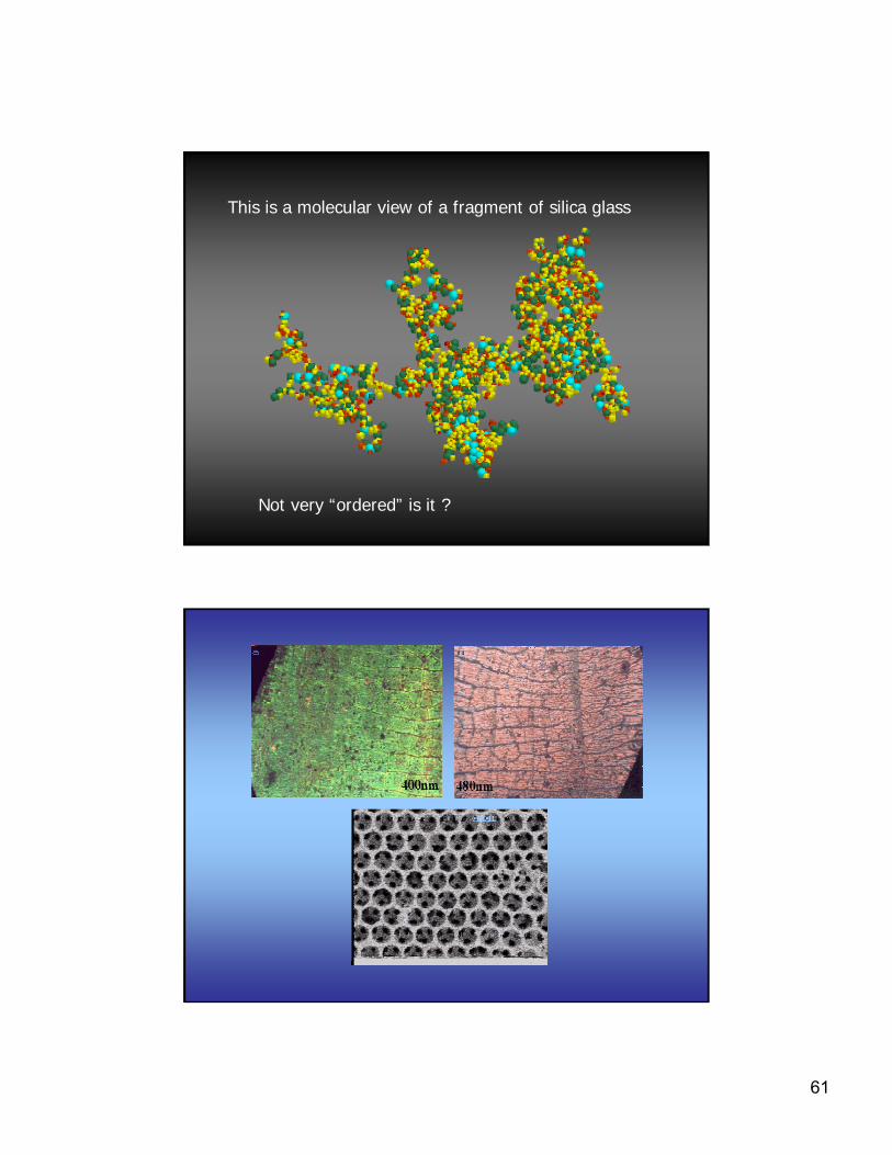
This is a molecular view of a fragment of silica glass
Not very “ordered” is it ?
62
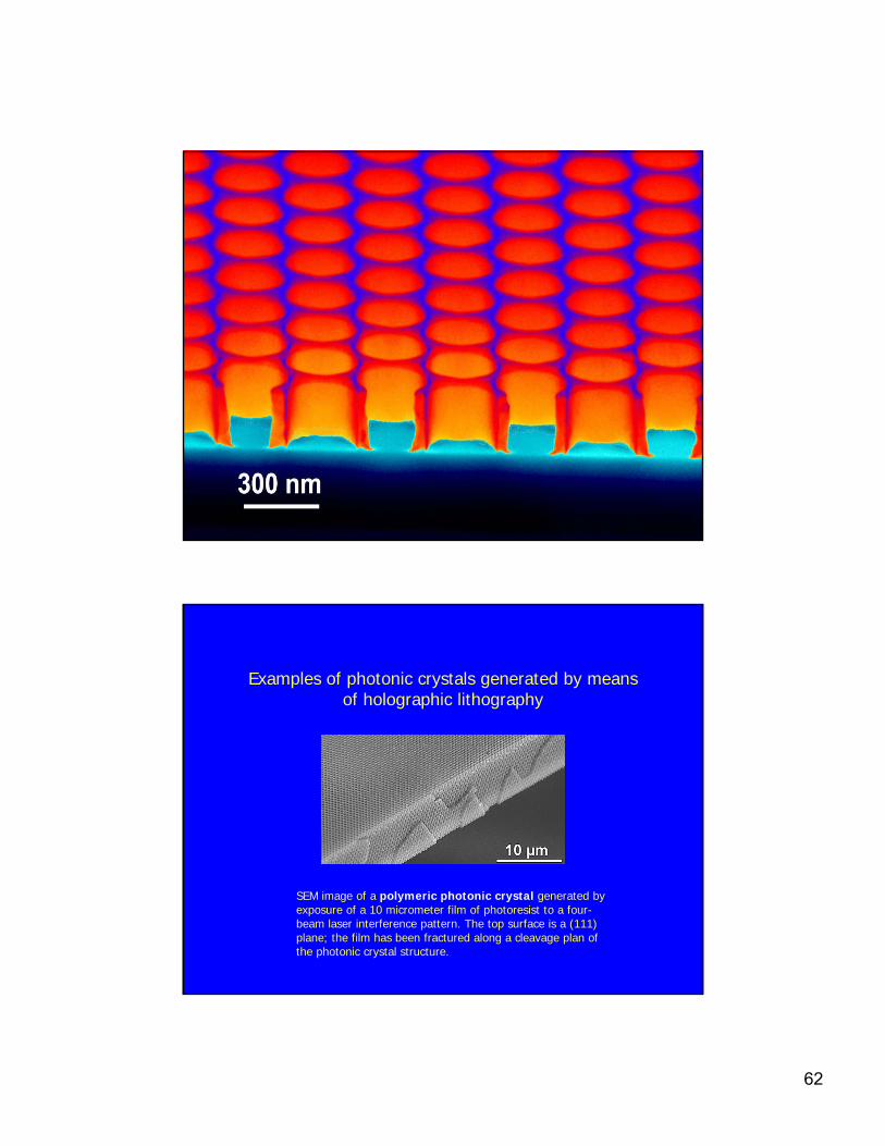
Examples of photonic crystals generated by means of holographic lithography
SEM image of a polymeric photonic crystal generated by exposure of a 10 micrometer film of photoresist to a four-beam laser interference pattern. The top surface is a (111) plane; the film has been fractured along a cleavage plan of the photonic crystal structure.
63
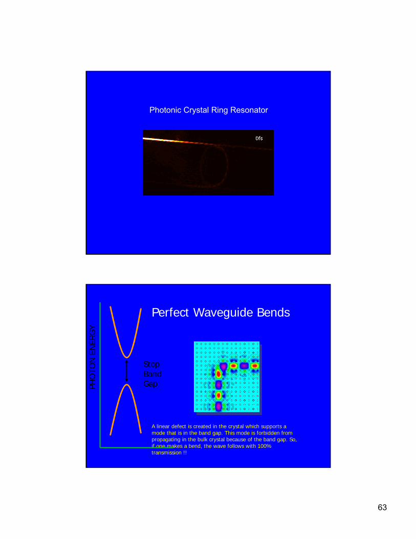
Photonic Crystal Ring Resonator
Perfect Waveguide Bends
A linear defect is created in the crystal which supports a mode that is in the band gap. This mode is forbidden from propagating in the bulk crystal because of the band gap. So, if one makes a bend, the wave follows with 100% transmission !!
PHO
TON
EN
ERG
Y
StopBand Gap
64
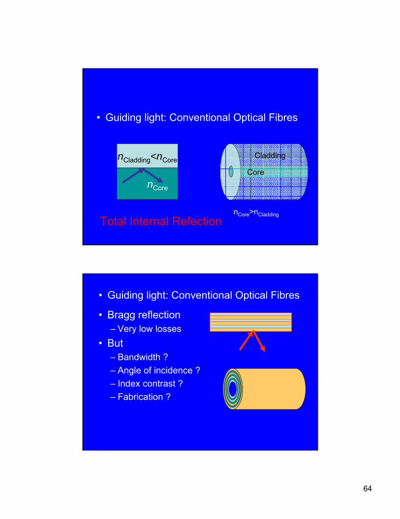
• Guiding light: Conventional Optical Fibres
Cladding
Core
nCore>nCladding
nCladding<nCore
nCore
Total Internal Refection
• Guiding light: Conventional Optical Fibres
• Bragg reflection– Very low losses
• But– Bandwidth ?– Angle of incidence ?– Index contrast ?– Fabrication ?
65
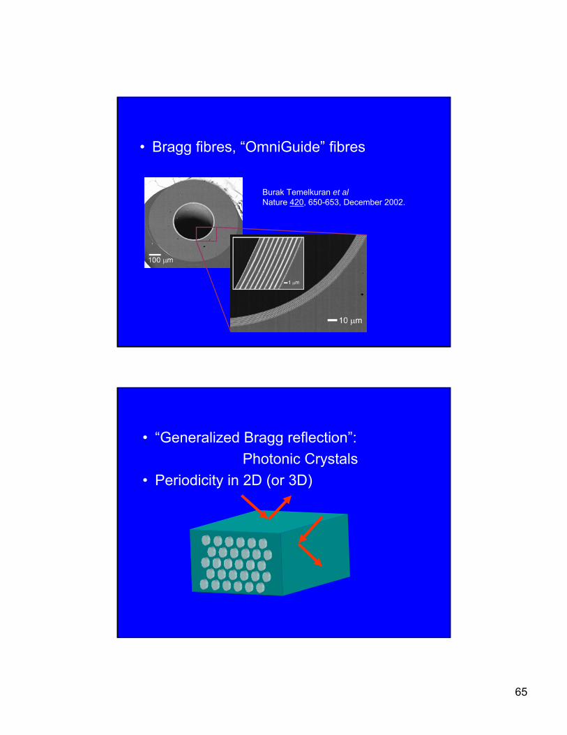
Burak Temelkuran et alNature 420, 650-653, December 2002.
• Bragg fibres, “OmniGuide” fibres
• “Generalized Bragg reflection”:Photonic Crystals
• Periodicity in 2D (or 3D)
66
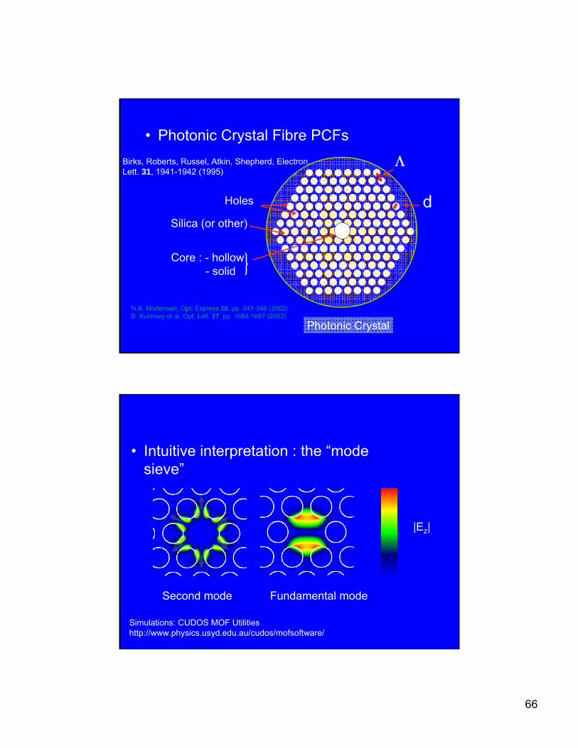
• Photonic Crystal Fibre PCFs
Λ
dHoles
Silica (or other)
Core : - hollow- solid
Photonic Crystal
Birks, Roberts, Russel, Atkin, Shepherd, Electron. Lett. 31, 1941-1942 (1995)
N.A. Mortensen, Opt. Express 10, pp. 341-348 (2002)B. Kuhlmey et al, Opt. Lett. 27, pp. 1684-1687 (2002)
• Intuitive interpretation : the “mode sieve”
Fundamental modeSecond mode
|Ez|
Simulations: CUDOS MOF Utilitieshttp://www.physics.usyd.edu.au/cudos/mofsoftware/
67
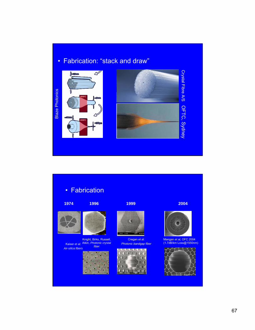
• Fabrication: “stack and draw”C
rystal Fibre A/S
OFTC
, Sydney
Bla
ze P
hoto
nics
• Fabrication
Knight, Birks, Russell, Atkin, Photonic crystal
fiber
Cregan et al.Photonic bandgap fiber
1974 1996 1999 2004
Kaiser et al.Air-silica fibers
Mangan et al, OFC 2004(1.7dB/km Loss@1550nm)
68
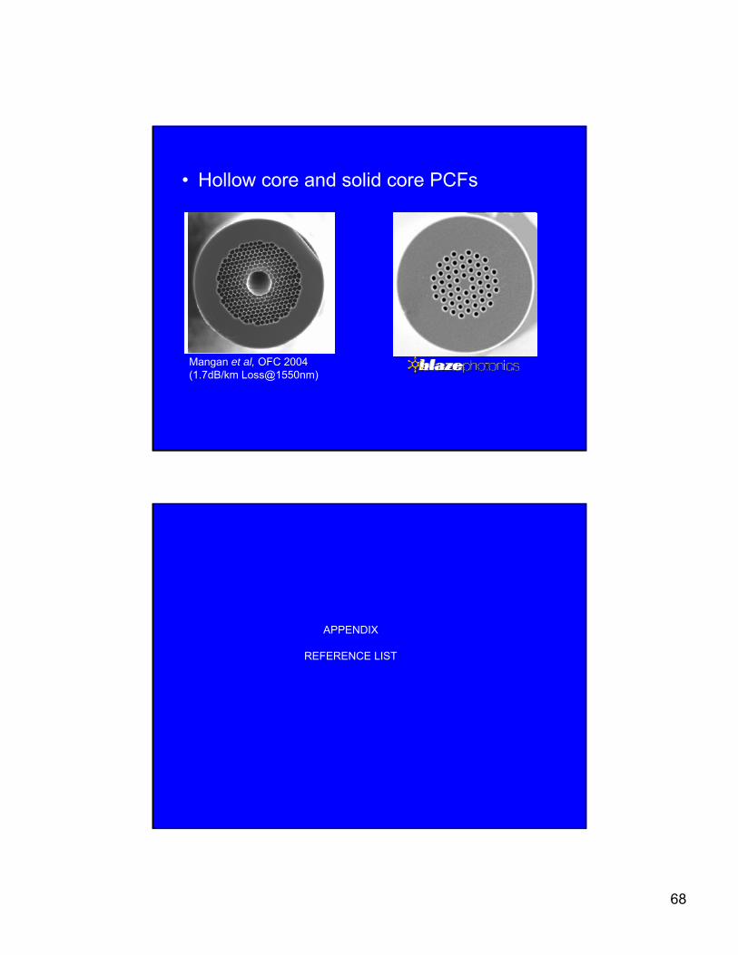
• Hollow core and solid core PCFs
Mangan et al, OFC 2004(1.7dB/km Loss@1550nm)
APPENDIX
REFERENCE LIST
69
1. Ben Fry “Organic Information Design”http://acg.media.mit.edu/people/fry/
2. Canadian Optical Internet (Project Canarie): http://www.canarie.ca/canet4/
3. Classic papers on Waveguide Raman: 1. Y. Leng, I. Imbert, J. Cipiani, S. Racine and R. Dupeyrat, Opt. Commun. 11, 66 (1974); J. Phys. (Paris), Colloq. C5 38, 253(1975). 2. R. Dupeyrat. Ber. Bunsenges. Phys. Chem. 85, 490 (1 981 ). 3. J. D. Swalen, J. Phys. Chem. 83, 1438 (1 979). 4. J. F. Rabolt, R. Santo and J. D. Swalen, Appl. Spectrosc. 33,549 (1 979) ; 34‘51 7 (1 980). 5. J. F. Rabolt, R. Santo, N. E. Schlotter and J. D. Swalen, 1BMJ. Res. Dev. 26, 209 (1 982). 6. J. D. Swalen and J. F. Rabolt, J. Phys. (Paris), 44, C10-15(1983).7. J. D. Swalen and J. F. Rabolt, in Spectroscopy of Surfaces, edited by R. J. H. Clark and R. E. Hester. Vol. 16. Chapt. 1, Wiley, Chichester (1 988)
4. Guided wave resonance Raman - Otto et al, Appl. Spectrosc. 57, 12, 2003
5. Farfield Inc sensors: http://www.farfield-scientific.com/index.asp6. Guided wave Non-resonance Raman: Otto et al J. Phys. Chem., 100, 3288, 19967. Optical waveguide light mode spectroscopy: using optical waveguides and diffraction
gratings to measure protein adsorption - Biosensors and BioelectronicsVolume 18, Issue 4 , April 2003, Pages 415-428
8. Nanoplasmonics and core shell nanoparticles: see www-ece.rice.edu/~halas/pubs.html Also Andrews et al Langmuir 1997, 13, 3744-3751 and Langmuir 1996, 12, 6389-6398
9. More on Nanoplasmonics – from Nanoplasmonics Vladimir M. Shalaev(Editor), Satoshi Kawata (Editor) Published:January 2007, ISBN:0444528385; also the review article in JOURNAL OF APPLIED PHYSICS 98, 011101 2005
Bio-plasmonics: Nano/micro structure of surface plasmon resonance devices for biomedicine in Optical and Quantum Electronics (2005) 37:1423–143
10. Biological optical fibres Proc Nat. Acad Sci, 3358–3363 March 9, 2004 vol. 101 no. 10.11. Lab-on-a-chip: Lab-on-a-chip with integrated optical transducers, Lab Chip, 2006, 6, 213–217.12. Ring resonator sensors: Optics Letters, Vol. 31, Issue 9, pp. 1319-1321 (2006)13. Polaritonics: PhD Thesishttp://www.people.fas.harvard.edu/~dward/Ward2005Thesis.pdfalso,David W. Ward, Eric R. Statz, Keith A. Nelson, Ryan M. Roth, and Richard M. Osgood:Terahertz wave generation and propagation in thin film lithium niobate produced by crystal ion slicing, Appl. Phys. Lett. 86, No. 2, 022908 (2005) DOI:10.1063/1.1850185. David W. Ward, Jaime D. Beers, T. Feurer, Eric R. Statz, Nikolay S. Stoyanov, and Keith A. Nelson: Coherent control of phonon-polaritons in a THz resonator fabricated with femtosecond laser machining, Opt. Lett. 29, 2671-2673 (2004). T. Feurer, Joshua C. Vaughan, and Keith A. Nelson:Spatiotemporal coherent control of lattice vibrational waves, Science 299, 374-377 (2003). Nikolay S. Stoyanov, David W. Ward, Thomas Feurer, and Keith A. Nelson:Integrateddiffractive THz elements, Appl. Phys. Lett. 82, No. 5, (2002). Nikolay S. Stoyanov, David W. Ward, Thomas Feurer, and Keith A. Nelson:Terahertzpolariton propagation in patterned materials, Nature Materials 1, 95-98 (2002).
70
14. Metamaterials with negative refractive index: see Webb, Yang, Ward and Nelson, Phys. Rev. E 70, 035602(R) (2004) and references cited therein15. Photonic Crystals: Key book is “Photonic Crystals”Publisher: Princeton University Press (1995) ISBN-10: 0691037442 or ISBN-13: 978-0691037448 ; also “Foundations of Photonic Crystal Fibers”by Zola et al., Imperial Coll. London Press, ISBN 1-86094-507-4 ; hundreds of literature references otherwise
Other references – General1. “Guided wave Photonics” Buckman, publ, Saunders1992, ISBN 0-03-033354-72. Fundamentals of Photonics, by Saleh and Teich, Wiley, 1991, ISBN 0-471-83965-5

![Optical Surface Microtraps based on Evanescent Waves · Optical Surface Microtraps based on Evanescent Waves Dissertation zur Erlangung des Doktorgrades an der ... [Fol02]. While](https://img.pdfslide.us/doc/110x75/5bdee43809d3f2647f8b63e5/optical-surface-microtraps-based-on-evanescent-optical-surface-microtraps-based.jpg)