Embed Size (px)
Citation preview

ORACLEOptimization with Recourse of Analog Circuits including Layout Extraction
ORACLEORACLEOOptimization with ptimization with RRecourse of ecourse of AAnalog nalog CCircuits including ircuits including LLayout ayout EExtractionxtraction
Yang Xu, Lawrence T. PileggiYang Xu, Lawrence T. Pileggi Stephen P. Boyd Stephen P. Boyd Carnegie Mellon University Carnegie Mellon University Stanford University Stanford University {{yangx,pileggi}@ece.cmu.eduyangx,pileggi}@ece.cmu.edu [email protected]@stanford.edu
28 June 2004

Slide 2
Analog/RF IC Cost CrisisAnalog/RF IC Cost Crisis
Analog design risk makes applicationAnalog design risk makes application--specific costs specific costs unaffordable for many applicationsunaffordable for many applications
Difficult to predict silicon realities w/o multiple silicon spinDifficult to predict silicon realities w/o multiple silicon spinss
Regularity and reuse required for predictability and costRegularity and reuse required for predictability and cost
ORACLE: new optimization framework for creation of an ORACLE: new optimization framework for creation of an applicationapplication--domaindomain--specific design fabricspecific design fabric
Configurable Design
Configurable Design
DesignApplication
DesignApplication
Apps #1 Apps #2 Apps #n
Optimization with Recourse

Slide 3
ORACLE Methodology ORACLE Methodology
Optimization for configurable analog/RF circuitsOptimization for configurable analog/RF circuitsInitial focus is on BEOL mask configurable fabrics Initial focus is on BEOL mask configurable fabrics Note that configurations are not limited to original scenariosNote that configurations are not limited to original scenarios

Slide 4
TwoTwo--stage design processstage design process
Divide circuit design process into 2 stagesDivide circuit design process into 2 stages1.1. Optimize for representative set of applications based on Optimize for representative set of applications based on
chosen circuit topology and shared design variableschosen circuit topology and shared design variables
2.2. Given common design fabric based on shared variables, Given common design fabric based on shared variables, optimally map a circuit design for a specific applicationoptimally map a circuit design for a specific application
Methodology relies on efficient optimization Methodology relies on efficient optimization formulationformulation
Stage 1 requires exploring large design space for many Stage 1 requires exploring large design space for many design scenariosdesign scenarios
Importantly, modeling accuracy is not critical for stage 1 to Importantly, modeling accuracy is not critical for stage 1 to define fabricdefine fabric
Detailed models and characterizations Detailed models and characterizations req’dreq’d for stage 2for stage 2
Slide 5
Geometric Program with Recourse (GPR)Geometric Program with Recourse (GPR)
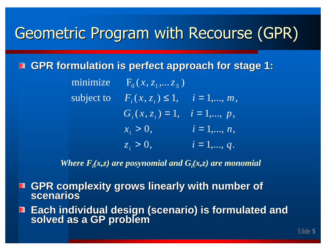
GPR formulation is perfect approach for stage 1:GPR formulation is perfect approach for stage 1:
GPR complexity grows linearly with number of GPR complexity grows linearly with number of scenariosscenariosEach individual design (scenario) is formulated and Each individual design (scenario) is formulated and solved as a GP problem solved as a GP problem
.,...,1 ,0
,,...,1 ,0
,,...,1 ,1),(
,,...,1 ,1),( subject to
),...,(F minimize 10
qiz
nix
pizxG
mizxF
zzx
i
i
ii
ii
S
=>=>===≤
Where Fi(x,z) are posynomial and Gi(x,z) are monomial

Slide 6
SiGeSiGe Low Noise Amplifier ExampleLow Noise Amplifier Example
Selection of circuit topology Selection of circuit topology and shared design variables and shared design variables is keyis key
Shared variables:Shared variables:Emitter length and widthInductor outer dimensionBiasing BJT multipliersBiasing ResistorsDecoupling caps
ApplicationApplication--specific variables:specific variables:BJT multiplierInductor turnsBias current and tuning caps
Configurable Configurable SiGeSiGe LNA designLNA designIBM 6HP IBM 6HP SiGeSiGe BiCMOSBiCMOS process process
(47GHz (47GHz ffTT NPN)NPN)

Slide 7
Frequency scalable LNA topologyFrequency scalable LNA topology
Individual GP formulations Individual GP formulations for each scenarios:for each scenarios:
12 design variables12 design variables
28 inequality constraints28 inequality constraints
Solved using MOSEKSolved using MOSEKTMTM
MATLAB toolboxMATLAB toolbox
Input and output center Input and output center frequency tunablefrequency tunable
SiGeSiGe BJT minimal NF is BJT minimal NF is frequency scalable:frequency scalable:
NFmin ∝ f, when f<<fT

Slide 8
Center frequency configurable Center frequency configurable LNAsLNAs
Consider center Consider center frequencies from 900MHz frequencies from 900MHz to 2.1GHzto 2.1GHz
13 design scenarios 13 design scenarios (200Mhz increments)(200Mhz increments)
5+75+7××13 = 96 design 13 = 96 design variablesvariables
28 28 ××13 = 364 design 13 = 364 design constraintsconstraints
Objective: Noise FigureObjective: Noise Figure
13 custom designs 13 custom designs produced as benchmark produced as benchmark
Performance comparable Performance comparable to custom designs with to custom designs with sufficient marginsufficient margin
1 1.2 1.4 1.6 1.8 2
x 109
1.4
1.45
1.5
1.55
1.6
1.65
1.7
Frequency scenarios
Noi
se F
igur
e (d
B)
Noise Figure Comparison
Configurable designsIndependent designs
Configurable
Custom

Slide 9
Power and gain configurable examplePower and gain configurable example
128 design scenarios by varying 128 design scenarios by varying power and gain specificationspower and gain specifications
Power spec: 12.5Power spec: 12.5 20mW by 0.5mW20mW by 0.5mW
Gain spec: 10Gain spec: 10 24dB by 2dB24dB by 2dB
Resulting GPR problemResulting GPR problem88××16=12816=128 design scenariosdesign scenarios5+75+7××128 = 901 design variables128 = 901 design variables28 28 ××128 = 3584 design constraints128 = 3584 design constraintsObjective: Noise FigureObjective: Noise Figure
128 custom designs produced as 128 custom designs produced as benchmarkbenchmark
EfficiencyEfficiency1.5sec for 128 configurable design in 1.5sec for 128 configurable design in 1.4GHz P4 machine1.4GHz P4 machine
1214
1618
20
10
15
20
250.06
0.07
0.08
0.09
0.1
0.11
Power Scenarios (mW)
Noise Figure Surcharge
Gain Scenarios (dB)
Noi
se F
igur
e (d
B)
1214
1618
20
10
15
20
251.2
1.4
1.6
1.8
2
Power Scenarios (mW)
NF of configurable LNAs
Gain Scenarios (dB)
Noi
se F
igu
re (d
B)

Slide 10
Configurable CMOS LNA exampleConfigurable CMOS LNA example
Vary center frequency from 1.5Vary center frequency from 1.5 5.5GHz by 500MHz5.5GHz by 500MHz9 design scenarios9 design scenarios
Objective: NF design surchargeObjective: NF design surcharge
NF’s comparable to custom NF’s comparable to custom designsdesigns
1.5 2 2.5 3 3.5 4 4.5 5 5.50.5
1
1.5
2
2.5
3
3.5NF of configurable designs and Independent designs
Center Frequency Scenarios (GHz)
Noi
se F
igur
e (d
B)
Slide 11
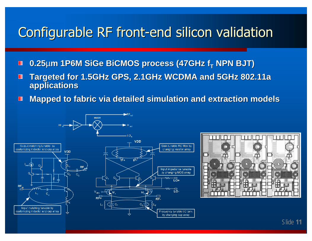
Configurable RF frontConfigurable RF front--end silicon validationend silicon validation
0.250.25µµm 1P6M SiGe BiCMOS process (47GHz m 1P6M SiGe BiCMOS process (47GHz ffTT NPN BJT)NPN BJT)
Targeted for 1.5GHz GPS, 2.1GHz WCDMA and 5GHz 802.11a Targeted for 1.5GHz GPS, 2.1GHz WCDMA and 5GHz 802.11a applicationsapplications
Mapped to fabric via detailed simulation and extraction modelsMapped to fabric via detailed simulation and extraction models

Slide 12
Regular Analog/RF IC Design FlowRegular Analog/RF IC Design Flow
Includes silicon Includes silicon characterization into the characterization into the design flowdesign flow
Offers reuse at the fabrics Offers reuse at the fabrics levellevel
Simplifies applicationSimplifies application--specific design cost and specific design cost and riskrisk
Select design scenarios to cover a domain of applications
Formulate optimization problem in terms of shared and
application-specific variables
Optimize all scenarios for sharedvariables for fabric construction
Refine original models to includeextracted characterization data
Re-optimize for a specific scenarioto find design specific variables
for metal mask construction
Extracted characterization
data from implementation
fabric
Slide 13
ConclusionsConclusions
Configurable analog/RF circuits are required for Configurable analog/RF circuits are required for many applications many applications
Reduce design risk and manufacturing costReduce design risk and manufacturing cost
ORACLE proposed for optimization frameworkORACLE proposed for optimization frameworkInitial focus on mask configurable RF frontInitial focus on mask configurable RF front--end end circuitscircuitsExamples demonstrate promising possibilitiesExamples demonstrate promising possibilities
Extending ORACLE to perform design centering Extending ORACLE to perform design centering to improve yieldto improve yield