Embed Size (px)
Citation preview
LLNL-BOOK-403314
Optics and multilayer coatings forEUVL systems
R. Soufli, S. Bajt, R. M. Hudyma, J. S. Taylor
April 29, 2008
EUV Lithography

Disclaimer
This document was prepared as an account of work sponsored by an agency of the United States government. Neither the United States government nor Lawrence Livermore National Security, LLC, nor any of their employees makes any warranty, expressed or implied, or assumes any legal liability or responsibility for the accuracy, completeness, or usefulness of any information, apparatus, product, or process disclosed, or represents that its use would not infringe privately owned rights. Reference herein to any specific commercial product, process, or service by trade name, trademark, manufacturer, or otherwise does not necessarily constitute or imply its endorsement, recommendation, or favoring by the United States government or Lawrence Livermore National Security, LLC. The views and opinions of authors expressed herein do not necessarily state or reflect those of the United States government or Lawrence Livermore National Security, LLC, and shall not be used for advertising or product endorsement purposes.
Chapter 4A
Optics and Multilayer Coatings for EUVL Systems
Regina Soufli, Saša Bajt, Russell M. Hudyma, and John S. Taylor
Contents 4A. 1 Introduction......................................................................................................................... 2 4A.2 Properties of EUVL Systems............................................................................................... 2

4A. 1 Introduction EUV lithography (EUVL) employs illumination wavelengths around 13.5 nm, and in many aspects it is considered an extension of optical lithography, which is used for the high-volume manufacturing (HVM) of today’s microprocessors. The EUV wavelength of illumination dictates the use of reflective optical elements (mirrors) as opposed to the refractive lenses used in conventional lithographic systems. Thus, EUVL tools are based on all-reflective concepts: they use multilayer (ML) coated optics for their illumination and projection systems, and they have a ML-coated reflective mask. 4A.2 Properties of EUVL Systems To achieve production-quality lithographic imaging, EUVL systems must be very well-corrected for aberrations. The overall wavefront error budget for an optical system scales with the wavelength of illumination. Compared to optical systems that operate at visible or near-visible wavelengths, EUVL error budgets translate into very tight wavefront (figure) specifications for the mirror substrates and coatings that comprise the EUVL system. The mirror surface roughness in the mid- and high-spatial frequency ranges (commonly referred to as “finish”) is also a crucial property because it affects the imaging contrast and throughput of the lithographic system. As a result, the figure and finish of mirror substrates and coatings in a production-scale EUVL system must be controlled to the order of subatomic dimensions. During the EUVL technology development that has been taking place in the past two decades, the aforementioned requirements imposed on the system wavefront error, on the mirror figure and finish, and on the reflective properties and lateral thickness control of EUV ML thin films have led to enormous advancements in optical substrate manufacturing, optics mounting and alignment techniques, and ML coating technology. Large-area ML optics with figure and finish of 0.1 to 0.2 nm rms have been fabricated and integrated in EUV optical systems with sub-diffraction-limited performance. Furthermore, ML coatings with normal-incidence experimental reflectivities of 70% have been demonstrated in the 11 to 14 nm wavelength range. Scientific areas such as solar physics, astronomy, x-ray microscopy, and plasma diagnostics that need similar instrumentation technology have greatly benefited by the improvements in EUV/x-ray optics motivated by EUVL. Sections 4B, 4C, and 4D summarize the basic principles of the optical design, substrate specification/manufacturing, and ML deposition of EUVL optics. In each case, the main challenges are emphasized and experimental results from state-of-the-art EUVL systems are presented as examples. For further details on the principles and theory behind several of the topics discussed in this Chapter, especially those relevant to Section 4D (ML interference coatings and interactions of EUV radiation with matter) the reader is referred to books by D. Attwood1 and E. Spiller2
References 1. D. T. Attwood, Soft X-rays and Extreme Ultraviolet Radiation, Principles and Applications, Cambridge University Press (1999). 2. E. Spiller, Soft X-ray Optics, SPIE Press, Bellingham, WA (1994).
Chapter 4B
Projection Systems for Extreme Ultraviolet Lithography
Russell M. Hudyma and Regina Soufli
Contents 4B.1 General EUVL Optical Design Considerations ................................................................. 4 4B.2 EUV Microsteppers.............................................................................................................. 6
4B.2.1 “10X” Microstepper ........................................................................................................ 6 4B.2.2 Micro-exposure tool (MET) ............................................................................................ 8
4B.3 Engineering Test Stand (ETS) .......................................................................................... 15 4B.4 Six-Mirror EUVL Projection Systems ............................................................................. 17
4B.4.1 Feasibility ...................................................................................................................... 17 4B.4.2 Concepts with concave primary mirrors ....................................................................... 18 4B.4.3 Concepts with convex primary mirrors......................................................................... 21 4B.4.4 Conclusions ................................................................................................................... 23
Acknowledgements ..................................................................................................................... 24 References.................................................................................................................................... 24
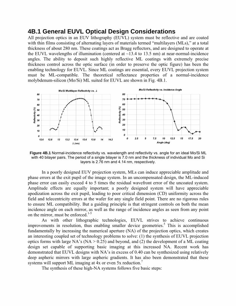
4B.1 General EUVL Optical Design Considerations All projection optics in an EUV lithography (EUVL) system must be reflective and are coated with thin films consisting of alternating layers of materials termed “multilayers (MLs),” at a total thickness of about 280 nm. These coatings act as Bragg reflectors, and are designed to operate at the EUVL wavelengths of illumination (centered at ~13.4 to 13.5 nm) at near-normal-incidence angles. The ability to deposit such highly reflective ML coatings with extremely precise thickness control across the optic surface (in order to preserve the optic figure) has been the enabling technology for EUVL. Since ML coatings are essential, every EUVL projection system must be ML-compatible. The theoretical reflectance properties of a normal-incidence molybdenum-silicon (Mo/Si) ML suited for EUVL are shown in Fig. 4B.1.
Figure 4B.1 Normal-incidence reflectivity vs. wavelength and reflectivity vs. angle for an ideal Mo/Si ML with 40 bilayer pairs. The period of a single bilayer is 7.0 nm and the thickness of individual Mo and Si
layers is 2.76 nm and 4.14 nm, respectively. In a poorly designed EUV projection system, MLs can induce appreciable amplitude and phase errors at the exit pupil of the image system. In an uncompensated design, the ML-induced phase error can easily exceed 4 to 5 times the residual wavefront error of the uncoated system. Amplitude effects are equally important; a poorly designed system will have appreciable apodization across the exit pupil, leading to poor critical dimension (CD) uniformity across the field and telecentricity errors at the wafer for any single field point. There are no rigorous rules to ensure ML compatibility. But a guiding principle is that stringent controls on both the mean incidence angle on each mirror, as well as the range of incidence angles as seen from any point on the mirror, must be enforced.1-5
As with other lithographic technologies, EUVL strives to achieve continuous improvements in resolution, thus enabling smaller device geometries.5 This is accomplished fundamentally by increasing the numerical aperture (NA) of the projection optics, which creates an interesting coupled set of technology problems to solve: (1) the synthesis of EUVL projection optics forms with large NA’s (NA > 0.25) and beyond, and (2) the development of a ML coating design set capable of supporting basic imaging at this increased NA. Recent work has demonstrated that EUVL designs with NA’s in excess of 0.40 can be synthesized using relatively deep aspheric mirrors with large aspheric gradients. It has also been demonstrated that these systems will support ML imaging at 4x or even 5x reduction.7 The synthesis of these high-NA systems follows five basic steps:

1. The synthesis of all-reflective or catoptric projection system concepts capable of correcting imaging aberrations at NA’s in excess of 0.25 over meaningful slit widths with an even number of reflections.
2. The characterization and correction of ML-induced amplitude errors at high NA. 3. The characterization and correction of ML-induced phase errors at high NA. 4. The simultaneous refinement of the complete projection systems (optics and ML
coatings) via damped least squared (DLS) optimization using specialized user-defined error functions.
5. A validation, via an analysis of the partial coherent imagery, that the canonical projection systems can meet lithographic imaging standards.
This process flow is illustrated in Fig. 4B.2.
Figure 4B.2 Necessary process flow to determine the extensibility of EUVL. The process starts by conceptualizing canonical EUV projection systems targeted at process nodes down to 15 nm. The
remaining tasks determine if these conceptual systems are (1) compatible with EUV MLs, and (2) support lithographic-quality imaging.
Since EUVL projection systems are all-reflective, there are several additional subtleties beyond simple ML compatibility and the dual-track optimization process to achieve a manufacturable solution. The aspheric mirrors used in an EUVL projection system must have both the peak departures and aspheric gradients carefully controlled to ensure both the fabrication and metrology process. First, the absolute aspheric departure from the best-fit sphere
sets the maximum number of fringes that the interferometer must accommodate. As the maximum number of fringes increases, the complexity of the compensation optics used to “null” the test wavefront generally increases. Second, the peak aspheric departure is a measure of the material that must be removed during the fabrication process. Since this removal process is performed with sub-aperture tools, excessive departures lead to excessive process times, which add to the risk of introducing mid-spatial-frequency errors due to process fluctuations. Perhaps even more important than the maximum aspheric departure is the aspheric gradient, or the change in aspheric sag as a function of lateral coordinates across the mirror surface. This sets the local fringe density that the interferometer’s sensor must resolve. At an empirical limit of approximately four pixels per fringe, the interferometry simply no longer has the accuracy with which to test the EUV surfaces. And to generate steeper gradients, higher-frequency tool functions in the polishing process are required. These higher-frequency tool functions have the tendency to increase the mid-spatial-frequency roughness (MSFR). To compound the problem, mid-spatial-frequency smoothing techniques do not work as well in regions of increased mirror slope. In addition to ML compatibility and the challenges of essentially tailoring aspheric mirrors that need to be figured to atomic dimensions, EUVL systems have the usual challenges related to the development of multimirror systems, including ray clearance, back working distance, volume claims for mounting interface, etc. Working distances and clearances are also driving issues, since mirror substrates need adequate thickness to overcome mount-induced deformations. Despite these challenges, EUV projection systems are a reality today, and several high-profile systems are enabling EUV researchers to continue to unlock the promise of EUV technology. 4B.2 EUV Microsteppers The semiconductor industry uses a reduced field image size at a similar optical resolution to that eventually intended to be adopted in production, and microsteppers to gain early learning on new technology nodes four to five years ahead of their introduction. Microsteppers allow manufacturers and researchers alike to develop and qualify new photoresists well before they are required for high-volume integrated circuit (IC) manufacturing. Microsteppers also allow researchers to investigate defect printability, test new reticle designs, and fabricate prototype ICs at the node of interest as well as provide early learning on tool-related technology challenges associated with sources, optics, lens aberrations, imaging effects, materials, metrology, reticles, photoresists, contamination, cost of ownership, reliability, and lifetime. In the field of EUV, both the “10X” microstepper and microexposure tool (MET) have played pivotal roles in the development of EUV technology and infrastructure. 4B.2.1 “10X” Microstepper Between 1997 and 2002, EUVL was given a tremendous technology push with developments made by the Virtual National Laboratory (VNL), which consists of Lawrence Livermore, Sandia, and Lawrence Berkeley National Laboratories (LLNL, SNL, and LBNL, respectively). Funding was supplied by the EUV Limited Liability Company (LLC)—a consortium formed by IC manufacturers Intel, AMD, IBM, Infineon, Micron, and Motorola. Much of the initial technology development work was performed using what was called the “10X” microstepper.8

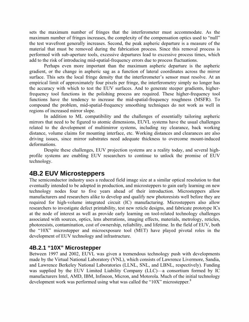
The 10X projection optics consist of a two-mirror objective arranged in a Schwarszchild form with a convex primary mirror and a concave secondary mirror, as light travels left to right from the patterned mask to the wafer. This objective is of the reverse telephoto type so that the back working distance is greater than the focal length of the objective. The projection optics were designed with a maximum centered NA of 0.30, but the aperture stop is decentered to produce a system with an unobscured circular aperture (Fig. 4B.3). The geometry constraints imposed by reasonable opto-mechanical considerations limit the NA of the off-axis bundle to 0.088 by design.
Figure 4B.3 10X microstepper projection optics illustrating the decentered aperture stop on the primary mirror M1.
For an object at infinity, the Schwarzschild objective is formed by two concentric spherical mirrors. The design is free from spherical aberration, coma, and astigmatism, provided that the ratio of concave radius to the convex radius (R2/R1) is equal to (√5+1)/(√5-1) or 2.618034. When the system is used in a microstepper at a reduction ratio, the object distance must be given some finite value. This means that the concave secondary mirror must be weakened to correct the spherical aberration and coma while maintaining the concentricity of the mirrors M1 and M2. For this 10x objective, the new R2/R1 ratio is 3.083498, which is in close agreement to an example provided by Kingslake.9 The resulting objective is free from spherical aberration, coma, and astigmatism at 0.088 NA, with the field curvature limiting the imaging performance. The residual root mean square (rms) composite wavefront error within a 280-µm square field of view as-designed is 0.055λ (λ = 13.4 nm), or 0.75 nm. The inward field curvature is approximately 0.80 µm when analyzed across the 400-µm-diameter field. These parameters are summarized in Table 4B.1. The 10X microstepper received an upgraded optics package in late 1998, with the figure error of both primary and secondary mirrors approaching 0.4-nm rms. By clocking the mirrors relative to each other, the subaperture wavefront was optimized to achieve a residual rms wavefront error of 0.045λ (0.6 nm). This rms value was derived from a 37-term Zernike expansion to the measured interferogram, representing an as-built wavefront error value that was actually lower than the design residual. In addition to the excellent mirror figure, the MSFR (mid-spatial frequency roughness corresponding to spatial periods of 1 mm-1 to 1 µm-1) achieved on both the primary and secondary mirrors was 0.13-nm rms and 0.20-nm rms, respectively. These MSFR values enabled low-flare imaging with measured flare levels on the order of 4%.
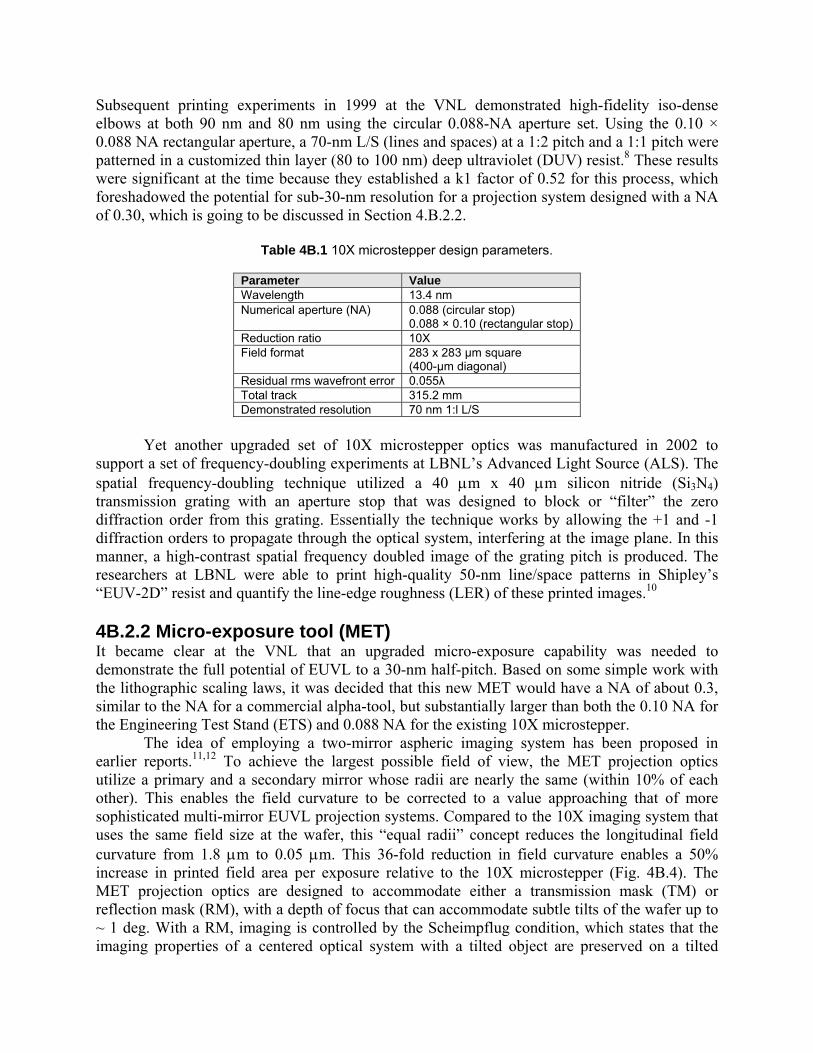
Subsequent printing experiments in 1999 at the VNL demonstrated high-fidelity iso-dense elbows at both 90 nm and 80 nm using the circular 0.088-NA aperture set. Using the 0.10 × 0.088 NA rectangular aperture, a 70-nm L/S (lines and spaces) at a 1:2 pitch and a 1:1 pitch were patterned in a customized thin layer (80 to 100 nm) deep ultraviolet (DUV) resist.8 These results were significant at the time because they established a k1 factor of 0.52 for this process, which foreshadowed the potential for sub-30-nm resolution for a projection system designed with a NA of 0.30, which is going to be discussed in Section 4.B.2.2.
Table 4B.1 10X microstepper design parameters.
Parameter Value Wavelength 13.4 nm Numerical aperture (NA) 0.088 (circular stop)
0.088 × 0.10 (rectangular stop) Reduction ratio 10X Field format 283 x 283 µm square
(400-µm diagonal) Residual rms wavefront error 0.055λ Total track 315.2 mm Demonstrated resolution 70 nm 1:l L/S
Yet another upgraded set of 10X microstepper optics was manufactured in 2002 to support a set of frequency-doubling experiments at LBNL’s Advanced Light Source (ALS). The spatial frequency-doubling technique utilized a 40 µm x 40 µm silicon nitride (Si3N4) transmission grating with an aperture stop that was designed to block or “filter” the zero diffraction order from this grating. Essentially the technique works by allowing the +1 and -1 diffraction orders to propagate through the optical system, interfering at the image plane. In this manner, a high-contrast spatial frequency doubled image of the grating pitch is produced. The researchers at LBNL were able to print high-quality 50-nm line/space patterns in Shipley’s “EUV-2D” resist and quantify the line-edge roughness (LER) of these printed images.10
4B.2.2 Micro-exposure tool (MET) It became clear at the VNL that an upgraded micro-exposure capability was needed to demonstrate the full potential of EUVL to a 30-nm half-pitch. Based on some simple work with the lithographic scaling laws, it was decided that this new MET would have a NA of about 0.3, similar to the NA for a commercial alpha-tool, but substantially larger than both the 0.10 NA for the Engineering Test Stand (ETS) and 0.088 NA for the existing 10X microstepper. The idea of employing a two-mirror aspheric imaging system has been proposed in earlier reports.11,12 To achieve the largest possible field of view, the MET projection optics utilize a primary and a secondary mirror whose radii are nearly the same (within 10% of each other). This enables the field curvature to be corrected to a value approaching that of more sophisticated multi-mirror EUVL projection systems. Compared to the 10X imaging system that uses the same field size at the wafer, this “equal radii” concept reduces the longitudinal field curvature from 1.8 µm to 0.05 µm. This 36-fold reduction in field curvature enables a 50% increase in printed field area per exposure relative to the 10X microstepper (Fig. 4B.4). The MET projection optics are designed to accommodate either a transmission mask (TM) or reflection mask (RM), with a depth of focus that can accommodate subtle tilts of the wafer up to ~ 1 deg. With a RM, imaging is controlled by the Scheimpflug condition, which states that the imaging properties of a centered optical system with a tilted object are preserved on a tilted

image plane (ignoring distortion). For a system used at finite conjugates, the image plane tilt is the object plane tilt scaled by the reduction ratio. A reflective mask can be tilted up to ~ 5 deg in the MET.
Figure 4B.4 The principal feature of the MET design is the reduction in field curvature, which allows focus
to be maintained across the entire tilted wafer plane. The image formed at the wafer with the 10X camerawould be outside the depth of focus due to the curvature of field. The y-axis is normalized to the
field height of the MET (3 mm), which represents the field of view at the reticle that is projected at 5x reduction at the wafer. Both tangential (T, dash line) and saggital (S, solid line) field curvatures are
shown. Layouts of the final optical design with reflection and transmission masks are shown in Figs. 4B.5 and 4B.6, respectively. Table 4B.2 summarizes the performance of the optical design relative to parameter goals. A large NA of 0.30 is attained by the use of a centered design, where the imaging bundles are centered on the optical axis. The centered design necessitates that the image passes through a hole in the primary mirror. Eccentric or off-axis pupil design forms are not feasible because the individual mirrors work at very fast conjugates. The residual aberrations simply grow too quickly to correct as the pupil moves off the optical axis. This fact forces the central obscuration on the exit pupil of the imaging system. To minimize the obscured pupil area (< 10%), the image plane must be kept close to the primary mirror. This reduces the clearance between the back of the primary mirror and the wafer. The vertex thickness of the primary mirror

was set to 20 mm to provide ample substrate stiffness, leaving only 5 mm of clearance between the back of the primary mirror and the wafer. This makes mechanical packaging of the primary mirror difficult and precludes the use of a grazing-incidence focus system.
Table 4B.2 MET projection optics performance summary (RM = reflection mask, TM = transmission mask).
Parameter Predicted Performance Wavelength 13.4 nm Numerical aperture 0.30 Focal length 102.5 mm Field format Type Length × width
Rectangular 600 µm ×200 µm
Mask compatibility RM & TM Reduction ratio (nominal) 5:1 Residual rms wavefront error (waves @ λ = 13.4 nm) Field point maximum Composite
0.054λ RM) 0.027λ (TM) 0.031λ (RM) 0.021λ (TM)
Resolution 30 nm Distortion (peak-to-valley static, nm) Chief ray
497.6 nm (RM) 2.24 nm (TM)
Depth of focus 200 nm Telecentricity error ∆y (nm) image/ ∆z (nm) focus
0.0148 nm/nm
Package Total track (mask/wafer) Overall length (vertex/vertex)
474.16 mm 275.60 mm
Working distances M1/wafer M2/mask
~ 5.0 mm ~ 113.56 mm
Aperture stop Accessible on M1 Peak aspheric departure M1 (primary) M2 (secondary)
3.82 µm 5.61 µm
Maximum aspheric slope M1 (primary) M2 (secondary)
-1.18 µm/mm -0.47 µm/mm
Angles of incidence, from normal M1 (max/min) M2 (max/min)
8.67°/2.54° 1.98°/0.67°
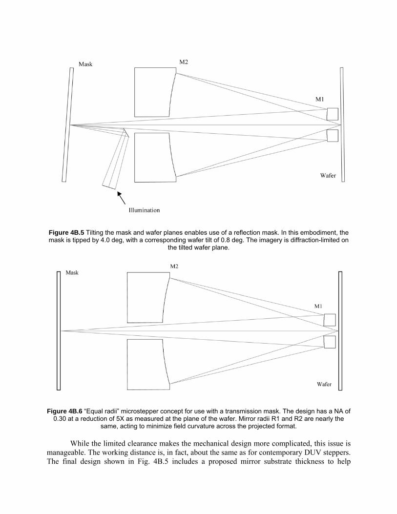
Figure 4B.5 Tilting the mask and wafer planes enables use of a reflection mask. In this embodiment, the mask is tipped by 4.0 deg, with a corresponding wafer tilt of 0.8 deg. The imagery is diffraction-limited on
the tilted wafer plane.
Figure 4B.6 “Equal radii” microstepper concept for use with a transmission mask. The design has a NA of
0.30 at a reduction of 5X as measured at the plane of the wafer. Mirror radii R1 and R2 are nearly the same, acting to minimize field curvature across the projected format.
While the limited clearance makes the mechanical design more complicated, this issue is manageable. The working distance is, in fact, about the same as for contemporary DUV steppers. The final design shown in Fig. 4B.5 includes a proposed mirror substrate thickness to help

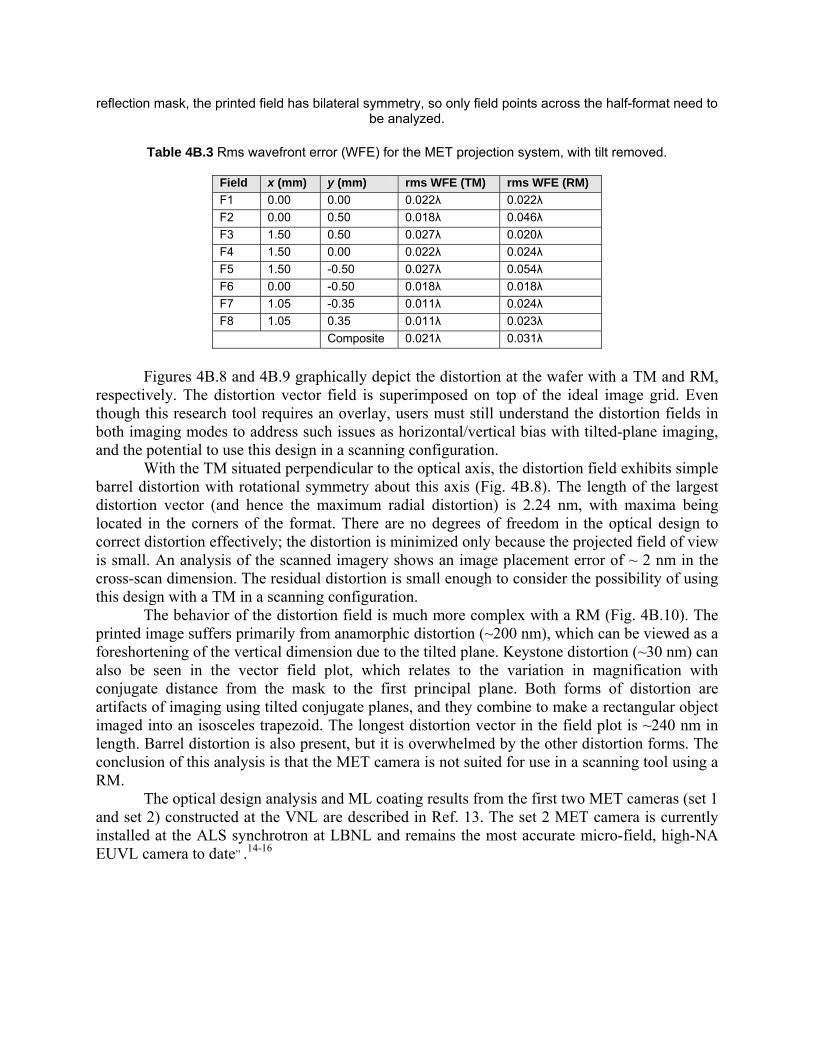
visualize clearance at the wafer and depict how the illumination is brought onto the mask. The design is optimized to work at a 5X reduction across a rectangular field of view of 600 × 200 µm at the wafer. While the field could be extended in the long dimension, the aspect ratio of 3:1 will help to simplify the design of the illumination system. The mask is tilted clockwise at 4.0 deg; the wafer has a corresponding counterclockwise tilt of 0.8 deg. This is the minimum tilt required to avoid interference between the incoming illumination and imaging bundle. With a RM, the composite rms wavefront error across a 600 × 200 µm rectangular field is 0.42 nm (0.031λ). This compares favorably to the composite rms wavefront of 0.28 nm (0.021λ) with a TM. The difference between the two imaging conditions is that the wavefront error varies more across the tilted conjugate planes. With a RM, the wavefront error varies from 0.24 nm (0.018λ) to 0.74 nm (0.055λ). The wavefront error variation with a TM is 0.15 nm (0.011λ) to 0.36 nm (0.027λ). While this variation across a tilted wafer would be troublesome in a production tool, causing field-dependent CD variations across the field, it is not a significant issue for this R&D tool. Since the MET projection optics are compatible with either a RM or a TM, the wavefront error and distortion analysis is performed in both modes of operation. The rms wavefront error was analyzed at nine distinct field points across the half-format as shown in Fig. 4B.7. This sampling is sufficient since the design has bilateral symmetry. The field size is set in RM mode because the maximum rms wavefront error at all field points must be less than 0.050λ. The rms wavefront error, less tilt, for each field point is listed in Table 4B.3. Using a TM, the field composite rms wavefront error is 0.28 nm (0.021λ). Residual field curvature and astigmatism present in the design cause a slight variation in the residual wavefront error across the field. With a RM, the field composite rms wavefront is 0.42 nm (0.031λ). There is more variation in the wavefront error in this case, due primarily to a variation in spherical aberration (fringe Zernike term Z9) across the field. This is a subtle effect that can be understood in the following way: with a tilted mask plane, the distance from the object surface to the first principal plane varies across the field, creating a field-dependent conjugate shift. Since the spherical aberration varies with conjugate distance, the spherical aberration will have field dependence.
Figure 4B.7 Analysis field points for the computation of rms wavefront error, incoherent square wave modulation transfer function (MTF), and 2D/3D partially coherent imagery, for the MET tool. With a
reflection mask, the printed field has bilateral symmetry, so only field points across the half-format need to be analyzed.
Table 4B.3 Rms wavefront error (WFE) for the MET projection system, with tilt removed.
Field x (mm) y (mm) rms WFE (TM) rms WFE (RM) F1 0.00 0.00 0.022λ 0.022λ F2 0.00 0.50 0.018λ 0.046λ F3 1.50 0.50 0.027λ 0.020λ F4 1.50 0.00 0.022λ 0.024λ F5 1.50 -0.50 0.027λ 0.054λ F6 0.00 -0.50 0.018λ 0.018λ F7 1.05 -0.35 0.011λ 0.024λ F8 1.05 0.35 0.011λ 0.023λ Composite 0.021λ 0.031λ
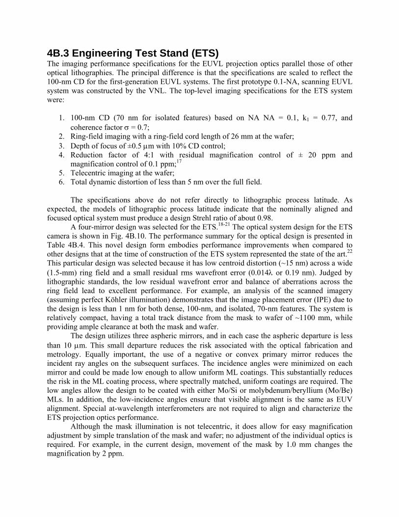
Figures 4B.8 and 4B.9 graphically depict the distortion at the wafer with a TM and RM, respectively. The distortion vector field is superimposed on top of the ideal image grid. Even though this research tool requires an overlay, users must still understand the distortion fields in both imaging modes to address such issues as horizontal/vertical bias with tilted-plane imaging, and the potential to use this design in a scanning configuration. With the TM situated perpendicular to the optical axis, the distortion field exhibits simple barrel distortion with rotational symmetry about this axis (Fig. 4B.8). The length of the largest distortion vector (and hence the maximum radial distortion) is 2.24 nm, with maxima being located in the corners of the format. There are no degrees of freedom in the optical design to correct distortion effectively; the distortion is minimized only because the projected field of view is small. An analysis of the scanned imagery shows an image placement error of ~ 2 nm in the cross-scan dimension. The residual distortion is small enough to consider the possibility of using this design with a TM in a scanning configuration. The behavior of the distortion field is much more complex with a RM (Fig. 4B.10). The printed image suffers primarily from anamorphic distortion (~200 nm), which can be viewed as a foreshortening of the vertical dimension due to the tilted plane. Keystone distortion (~30 nm) can also be seen in the vector field plot, which relates to the variation in magnification with conjugate distance from the mask to the first principal plane. Both forms of distortion are artifacts of imaging using tilted conjugate planes, and they combine to make a rectangular object imaged into an isosceles trapezoid. The longest distortion vector in the field plot is ~240 nm in length. Barrel distortion is also present, but it is overwhelmed by the other distortion forms. The conclusion of this analysis is that the MET camera is not suited for use in a scanning tool using a RM. The optical design analysis and ML coating results from the first two MET cameras (set 1 and set 2) constructed at the VNL are described in Ref. 13. The set 2 MET camera is currently installed at the ALS synchrotron at LBNL and remains the most accurate micro-field, high-NA EUVL camera to date,, .14-16
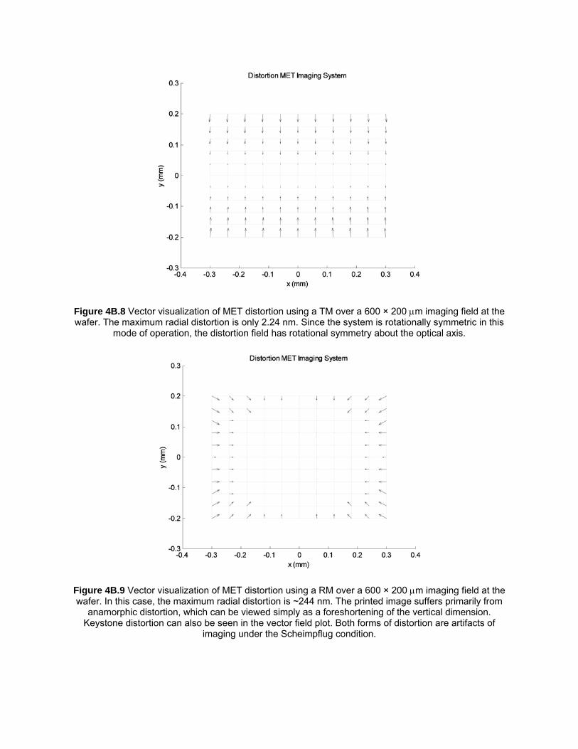
Figure 4B.8 Vector visualization of MET distortion using a TM over a 600 × 200 µm imaging field at the wafer. The maximum radial distortion is only 2.24 nm. Since the system is rotationally symmetric in this
mode of operation, the distortion field has rotational symmetry about the optical axis.
Figure 4B.9 Vector visualization of MET distortion using a RM over a 600 × 200 µm imaging field at the wafer. In this case, the maximum radial distortion is ~244 nm. The printed image suffers primarily from
anamorphic distortion, which can be viewed simply as a foreshortening of the vertical dimension. Keystone distortion can also be seen in the vector field plot. Both forms of distortion are artifacts of
imaging under the Scheimpflug condition.
4B.3 Engineering Test Stand (ETS) The imaging performance specifications for the EUVL projection optics parallel those of other optical lithographies. The principal difference is that the specifications are scaled to reflect the 100-nm CD for the first-generation EUVL systems. The first prototype 0.1-NA, scanning EUVL system was constructed by the VNL. The top-level imaging specifications for the ETS system were:
1. 100-nm CD (70 nm for isolated features) based on NA NA = 0.1, k1 = 0.77, and coherence factor σ = 0.7;
2. Ring-field imaging with a ring-field cord length of 26 mm at the wafer; 3. Depth of focus of ±0.5 µm with 10% CD control; 4. Reduction factor of 4:1 with residual magnification control of ± 20 ppm and
magnification control of 0.1 ppm;17 5. Telecentric imaging at the wafer; 6. Total dynamic distortion of less than 5 nm over the full field.
The specifications above do not refer directly to lithographic process latitude. As expected, the models of lithographic process latitude indicate that the nominally aligned and focused optical system must produce a design Strehl ratio of about 0.98. A four-mirror design was selected for the ETS.18-21 The optical system design for the ETS camera is shown in Fig. 4B.10. The performance summary for the optical design is presented in Table 4B.4. This novel design form embodies performance improvements when compared to other designs that at the time of construction of the ETS system represented the state of the art.22 This particular design was selected because it has low centroid distortion (~15 nm) across a wide (1.5-mm) ring field and a small residual rms wavefront error (0.014λ or 0.19 nm). Judged by lithographic standards, the low residual wavefront error and balance of aberrations across the ring field lead to excellent performance. For example, an analysis of the scanned imagery (assuming perfect Köhler illumination) demonstrates that the image placement error (IPE) due to the design is less than 1 nm for both dense, 100-nm, and isolated, 70-nm features. The system is relatively compact, having a total track distance from the mask to wafer of ~1100 mm, while providing ample clearance at both the mask and wafer. The design utilizes three aspheric mirrors, and in each case the aspheric departure is less than 10 µm. This small departure reduces the risk associated with the optical fabrication and metrology. Equally important, the use of a negative or convex primary mirror reduces the incident ray angles on the subsequent surfaces. The incidence angles were minimized on each mirror and could be made low enough to allow uniform ML coatings. This substantially reduces the risk in the ML coating process, where spectrally matched, uniform coatings are required. The low angles allow the design to be coated with either Mo/Si or molybdenum/beryllium (Mo/Be) MLs. In addition, the low-incidence angles ensure that visible alignment is the same as EUV alignment. Special at-wavelength interferometers are not required to align and characterize the ETS projection optics performance. Although the mask illumination is not telecentric, it does allow for easy magnification adjustment by simple translation of the mask and wafer; no adjustment of the individual optics is required. For example, in the current design, movement of the mask by 1.0 mm changes the magnification by 2 ppm.
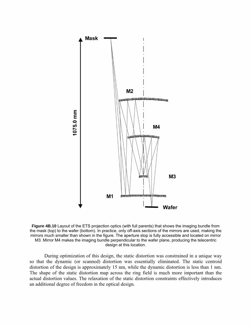
Figure 4B.10 Layout of the ETS projection optics (with full parents) that shows the imaging bundle from
the mask (top) to the wafer (bottom). In practice, only off-axis sections of the mirrors are used, making the mirrors much smaller than shown in the figure. The aperture stop is fully accessible and located on mirror
M3. Mirror M4 makes the imaging bundle perpendicular to the wafer plane, producing the telecentric design at this location.
During optimization of this design, the static distortion was constrained in a unique way so that the dynamic (or scanned) distortion was essentially eliminated. The static centroid distortion of the design is approximately 15 nm, while the dynamic distortion is less than 1 nm. The shape of the static distortion map across the ring field is much more important than the actual distortion values. The relaxation of the static distortion constraints effectively introduces an additional degree of freedom in the optical design.
Two ETS cameras were constructed at the VNL, set 1 and set 2, the latter with improved optics figure that resulted in improved system resolution. The experimental results from the ETS optics fabrication and ML coatings are described in Refs. 23 and 24.
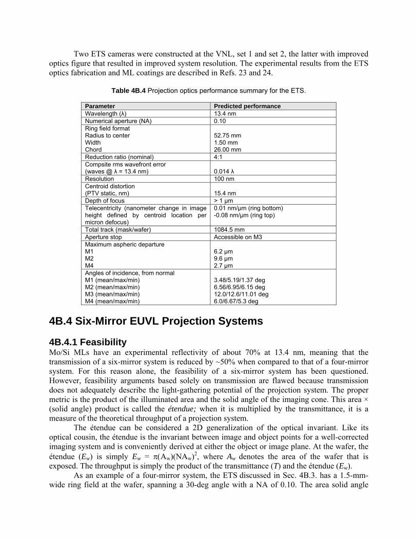
Table 4B.4 Projection optics performance summary for the ETS.
Parameter Predicted performance Wavelength (λ) 13.4 nm Numerical aperture (NA) 0.10 Ring field format Radius to center Width Chord
52.75 mm 1.50 mm 26.00 mm
Reduction ratio (nominal) 4:1 Compsite rms wavefront error (waves @ λ = 13.4 nm)
0.014 λ
Resolution 100 nm Centroid distortion (PTV static, nm)
15.4 nm
Depth of focus > 1 µm Telecentricity (nanometer change in image height defined by centroid location per micron defocus)
0.01 nm/µm (ring bottom) -0.08 nm/µm (ring top)
Total track (mask/wafer) 1084.5 mm Aperture stop Accessible on M3 Maximum aspheric departure M1 M2 M4
6.2 µm 9.6 µm 2.7 µm
Angles of incidence, from normal M1 (mean/max/min) M2 (mean/max/min) M3 (mean/max/min) M4 (mean/max/min)
3.48/5.19/1.37 deg 6.56/6.95/6.15 deg 12.0/12.6/11.01 deg 6.0/6.67/5.3 deg
4B.4 Six-Mirror EUVL Projection Systems 4B.4.1 Feasibility Mo/Si MLs have an experimental reflectivity of about 70% at 13.4 nm, meaning that the transmission of a six-mirror system is reduced by ~50% when compared to that of a four-mirror system. For this reason alone, the feasibility of a six-mirror system has been questioned. However, feasibility arguments based solely on transmission are flawed because transmission does not adequately describe the light-gathering potential of the projection system. The proper metric is the product of the illuminated area and the solid angle of the imaging cone. This area × (solid angle) product is called the étendue; when it is multiplied by the transmittance, it is a measure of the theoretical throughput of a projection system. The étendue can be considered a 2D generalization of the optical invariant. Like its optical cousin, the étendue is the invariant between image and object points for a well-corrected imaging system and is conveniently derived at either the object or image plane. At the wafer, the étendue (Ew) is simply Ew = π(Aw)(NAw)2, where Aw denotes the area of the wafer that is exposed. The throughput is simply the product of the transmittance (T) and the étendue (Ew). As an example of a four-mirror system, the ETS discussed in Sec. 4B.3. has a 1.5-mm-wide ring field at the wafer, spanning a 30-deg angle with a NA of 0.10. The area solid angle
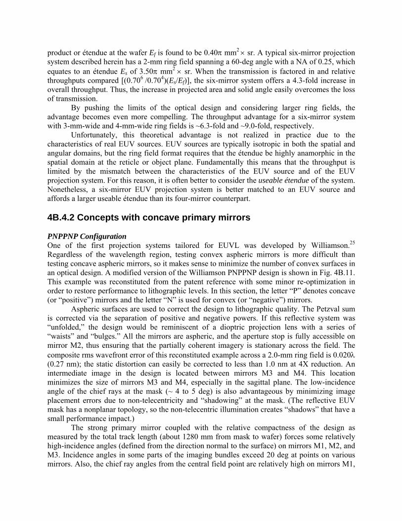
product or étendue at the wafer Ef is found to be 0.40π mm2 × sr. A typical six-mirror projection system described herein has a 2-mm ring field spanning a 60-deg angle with a NA of 0.25, which equates to an étendue Es of 3.50π mm2 × sr. When the transmission is factored in and relative throughputs compared [(0.706 /0.704)(Es/Ef)], the six-mirror system offers a 4.3-fold increase in overall throughput. Thus, the increase in projected area and solid angle easily overcomes the loss of transmission. By pushing the limits of the optical design and considering larger ring fields, the advantage becomes even more compelling. The throughput advantage for a six-mirror system with 3-mm-wide and 4-mm-wide ring fields is ~6.3-fold and ~9.0-fold, respectively. Unfortunately, this theoretical advantage is not realized in practice due to the characteristics of real EUV sources. EUV sources are typically isotropic in both the spatial and angular domains, but the ring field format requires that the étendue be highly anamorphic in the spatial domain at the reticle or object plane. Fundamentally this means that the throughput is limited by the mismatch between the characteristics of the EUV source and of the EUV projection system. For this reason, it is often better to consider the useable étendue of the system. Nonetheless, a six-mirror EUV projection system is better matched to an EUV source and affords a larger useable étendue than its four-mirror counterpart. 4B.4.2 Concepts with concave primary mirrors PNPPNP Configuration One of the first projection systems tailored for EUVL was developed by Williamson.25 Regardless of the wavelength region, testing convex aspheric mirrors is more difficult than testing concave aspheric mirrors, so it makes sense to minimize the number of convex surfaces in an optical design. A modified version of the Williamson PNPPNP design is shown in Fig. 4B.11. This example was reconstituted from the patent reference with some minor re-optimization in order to restore performance to lithographic levels. In this section, the letter “P” denotes concave (or “positive”) mirrors and the letter “N” is used for convex (or “negative”) mirrors. Aspheric surfaces are used to correct the design to lithographic quality. The Petzval sum is corrected via the separation of positive and negative powers. If this reflective system was “unfolded,” the design would be reminiscent of a dioptric projection lens with a series of “waists” and “bulges.” All the mirrors are aspheric, and the aperture stop is fully accessible on mirror M2, thus ensuring that the partially coherent imagery is stationary across the field. The composite rms wavefront error of this reconstituted example across a 2.0-mm ring field is 0.020λ (0.27 nm); the static distortion can easily be corrected to less than 1.0 nm at 4X reduction. An intermediate image in the design is located between mirrors M3 and M4. This location minimizes the size of mirrors M3 and M4, especially in the sagittal plane. The low-incidence angle of the chief rays at the mask (~ 4 to 5 deg) is also advantageous by minimizing image placement errors due to non-telecentricity and “shadowing” at the mask. (The reflective EUV mask has a nonplanar topology, so the non-telecentric illumination creates “shadows” that have a small performance impact.) The strong primary mirror coupled with the relative compactness of the design as measured by the total track length (about 1280 mm from mask to wafer) forces some relatively high-incidence angles (defined from the direction normal to the surface) on mirrors M1, M2, and M3. Incidence angles in some parts of the imaging bundles exceed 20 deg at points on various mirrors. Also, the chief ray angles from the central field point are relatively high on mirrors M1,

M2, and M3. These factors would conspire to add complications during the ML re-optimization effort.
Figure 4B.11 Modified six-mirror PNPPNP EUVL projection optics described by Williamson.25 The basic
design was modified to reduce the incidence angles on each of the surfaces. The chief ray incidence angles (central field point) are as follows: mask, 4.0 deg; M1, 10.1 deg; M2, 16.7 deg; M3, 13.3 deg; M4,
2.4 deg; M5, 11.1 deg; and M6, 3.8 deg. The design suffers a bit from large peak aspheric departures and relatively large aspheric gradients. In particular, mirrors M2 and M5 will be more difficult to test than the other mirrors in the system. The distance from the vertex of mirror M5 to the wafer is only 26 mm, which means that the back working distance of this particular embodiment is a bit strained. But not to lose sight of the basic idea, several improvements can be made. Using this basic PNPPNP formulation, ML compatibility is improved by increasing the total track to 1500 mm, while keeping the ring field radius fixed. This effectively stretches the optical design and reduces the apparent offset of the field at the mask. The ray angles at each surface are reduced ~10% using this technique. Improvements of several millimeters also can be made to the back working distance with additional detailed design effort. PPNPNP Configuration Assuming that the first mirror will take positive optical power, let us imagine a new projection system. By distributing the positive power between the primary and secondary mirrors, low-incidence angles can be achieved to promote ML compatibility. With the stop at M2, the distortion contribution from this surface is nulled. Now the position of the entrance pupil can be adjusted to null the tangential astigmatism contribution from the base sphere of M1. The relatively low power of M1 and the low chief ray height also reduce the distortion contribution from this surface. Now the strong convex tertiary M3 can be used to compensate for the low-order astigmatism and distortion. The negative convex mirrors are also used in such a way to minimize and nearly correct the Petzval sum independently n each half of the design. The result of this thought process is the PPNPNP design shown in Fig. 4B.12.26
The fundamental layout enables a low mean incidence angle at each mirror, giving the design a high degree of ML compatibility. The intermediate image is located between mirrors M4 and M5 to maximize ray clearance in the aft end of the system. At the wafer, the NA is 0.25 and the ring field width is 2.0 mm (centered on a radius of 30 mm). The composite rms wavefront error is 0.018λ (0.24 nm, λ = 13.4 nm), and the static distortion is corrected to better
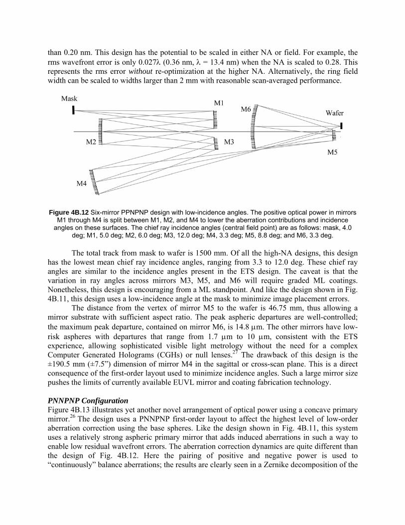
than 0.20 nm. This design has the potential to be scaled in either NA or field. For example, the rms wavefront error is only 0.027λ (0.36 nm, λ = 13.4 nm) when the NA is scaled to 0.28. This represents the rms error without re-optimization at the higher NA. Alternatively, the ring field width can be scaled to widths larger than 2 mm with reasonable scan-averaged performance.
Figure 4B.12 Six-mirror PPNPNP design with low-incidence angles. The positive optical power in mirrors
M1 through M4 is split between M1, M2, and M4 to lower the aberration contributions and incidence angles on these surfaces. The chief ray incidence angles (central field point) are as follows: mask, 4.0
deg; M1, 5.0 deg; M2, 6.0 deg; M3, 12.0 deg; M4, 3.3 deg; M5, 8.8 deg; and M6, 3.3 deg. The total track from mask to wafer is 1500 mm. Of all the high-NA designs, this design has the lowest mean chief ray incidence angles, ranging from 3.3 to 12.0 deg. These chief ray angles are similar to the incidence angles present in the ETS design. The caveat is that the variation in ray angles across mirrors M3, M5, and M6 will require graded ML coatings. Nonetheless, this design is encouraging from a ML standpoint. And like the design shown in Fig. 4B.11, this design uses a low-incidence angle at the mask to minimize image placement errors. The distance from the vertex of mirror M5 to the wafer is 46.75 mm, thus allowing a mirror substrate with sufficient aspect ratio. The peak aspheric departures are well-controlled; the maximum peak departure, contained on mirror M6, is 14.8 µm. The other mirrors have low-risk aspheres with departures that range from 1.7 µm to 10 µm, consistent with the ETS experience, allowing sophisticated visible light metrology without the need for a complex Computer Generated Holograms (CGHs) or null lenses.27 The drawback of this design is the ±190.5 mm (±7.5”) dimension of mirror M4 in the sagittal or cross-scan plane. This is a direct consequence of the first-order layout used to minimize incidence angles. Such a large mirror size pushes the limits of currently available EUVL mirror and coating fabrication technology. PNNPNP Configuration Figure 4B.13 illustrates yet another novel arrangement of optical power using a concave primary mirror.26 The design uses a PNNPNP first-order layout to affect the highest level of low-order aberration correction using the base spheres. Like the design shown in Fig. 4B.11, this system uses a relatively strong aspheric primary mirror that adds induced aberrations in such a way to enable low residual wavefront errors. The aberration correction dynamics are quite different than the design of Fig. 4B.12. Here the pairing of positive and negative power is used to “continuously” balance aberrations; the results are clearly seen in a Zernike decomposition of the
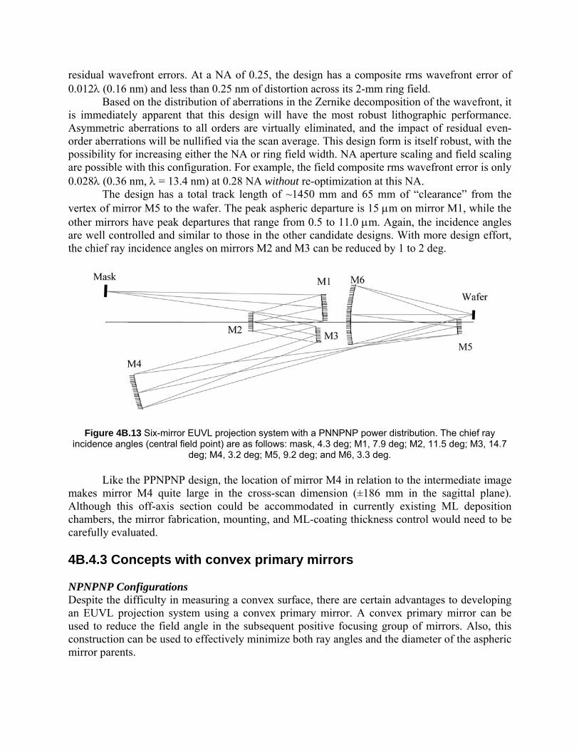
residual wavefront errors. At a NA of 0.25, the design has a composite rms wavefront error of 0.012λ (0.16 nm) and less than 0.25 nm of distortion across its 2-mm ring field. Based on the distribution of aberrations in the Zernike decomposition of the wavefront, it is immediately apparent that this design will have the most robust lithographic performance. Asymmetric aberrations to all orders are virtually eliminated, and the impact of residual even-order aberrations will be nullified via the scan average. This design form is itself robust, with the possibility for increasing either the NA or ring field width. NA aperture scaling and field scaling are possible with this configuration. For example, the field composite rms wavefront error is only 0.028λ (0.36 nm, λ = 13.4 nm) at 0.28 NA without re-optimization at this NA. The design has a total track length of ~1450 mm and 65 mm of “clearance” from the vertex of mirror M5 to the wafer. The peak aspheric departure is 15 µm on mirror M1, while the other mirrors have peak departures that range from 0.5 to 11.0 µm. Again, the incidence angles are well controlled and similar to those in the other candidate designs. With more design effort, the chief ray incidence angles on mirrors M2 and M3 can be reduced by 1 to 2 deg.
Figure 4B.13 Six-mirror EUVL projection system with a PNNPNP power distribution. The chief ray incidence angles (central field point) are as follows: mask, 4.3 deg; M1, 7.9 deg; M2, 11.5 deg; M3, 14.7
deg; M4, 3.2 deg; M5, 9.2 deg; and M6, 3.3 deg. Like the PPNPNP design, the location of mirror M4 in relation to the intermediate image makes mirror M4 quite large in the cross-scan dimension (±186 mm in the sagittal plane). Although this off-axis section could be accommodated in currently existing ML deposition chambers, the mirror fabrication, mounting, and ML-coating thickness control would need to be carefully evaluated. 4B.4.3 Concepts with convex primary mirrors NPNPNP Configurations Despite the difficulty in measuring a convex surface, there are certain advantages to developing an EUVL projection system using a convex primary mirror. A convex primary mirror can be used to reduce the field angle in the subsequent positive focusing group of mirrors. Also, this construction can be used to effectively minimize both ray angles and the diameter of the aspheric mirror parents.
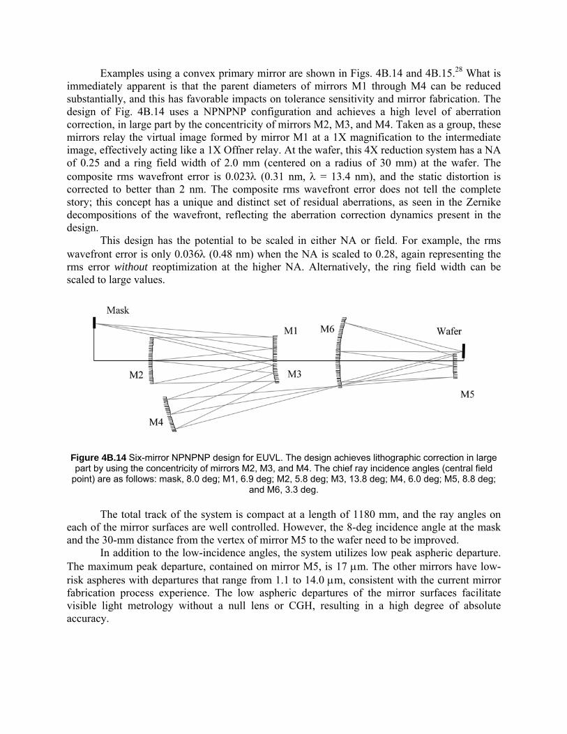
Examples using a convex primary mirror are shown in Figs. 4B.14 and 4B.15.28 What is immediately apparent is that the parent diameters of mirrors M1 through M4 can be reduced substantially, and this has favorable impacts on tolerance sensitivity and mirror fabrication. The design of Fig. 4B.14 uses a NPNPNP configuration and achieves a high level of aberration correction, in large part by the concentricity of mirrors M2, M3, and M4. Taken as a group, these mirrors relay the virtual image formed by mirror M1 at a 1X magnification to the intermediate image, effectively acting like a 1X Offner relay. At the wafer, this 4X reduction system has a NA of 0.25 and a ring field width of 2.0 mm (centered on a radius of 30 mm) at the wafer. The composite rms wavefront error is 0.023λ (0.31 nm, λ = 13.4 nm), and the static distortion is corrected to better than 2 nm. The composite rms wavefront error does not tell the complete story; this concept has a unique and distinct set of residual aberrations, as seen in the Zernike decompositions of the wavefront, reflecting the aberration correction dynamics present in the design. This design has the potential to be scaled in either NA or field. For example, the rms wavefront error is only 0.036λ (0.48 nm) when the NA is scaled to 0.28, again representing the rms error without reoptimization at the higher NA. Alternatively, the ring field width can be scaled to large values.
Figure 4B.14 Six-mirror NPNPNP design for EUVL. The design achieves lithographic correction in large part by using the concentricity of mirrors M2, M3, and M4. The chief ray incidence angles (central field
point) are as follows: mask, 8.0 deg; M1, 6.9 deg; M2, 5.8 deg; M3, 13.8 deg; M4, 6.0 deg; M5, 8.8 deg; and M6, 3.3 deg.
The total track of the system is compact at a length of 1180 mm, and the ray angles on each of the mirror surfaces are well controlled. However, the 8-deg incidence angle at the mask and the 30-mm distance from the vertex of mirror M5 to the wafer need to be improved. In addition to the low-incidence angles, the system utilizes low peak aspheric departure. The maximum peak departure, contained on mirror M5, is 17 µm. The other mirrors have low-risk aspheres with departures that range from 1.1 to 14.0 µm, consistent with the current mirror fabrication process experience. The low aspheric departures of the mirror surfaces facilitate visible light metrology without a null lens or CGH, resulting in a high degree of absolute accuracy.
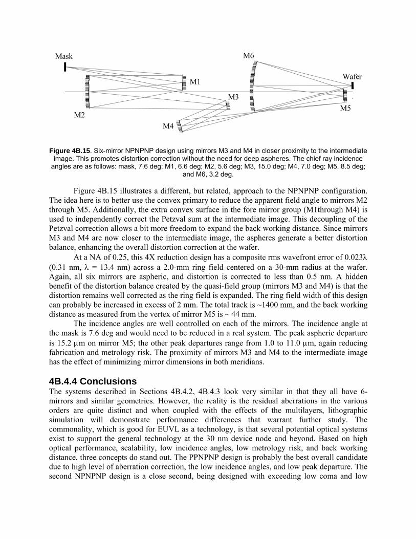
Figure 4B.15. Six-mirror NPNPNP design using mirrors M3 and M4 in closer proximity to the intermediate
image. This promotes distortion correction without the need for deep aspheres. The chief ray incidence angles are as follows: mask, 7.6 deg; M1, 6.6 deg; M2, 5.6 deg; M3, 15.0 deg; M4, 7.0 deg; M5, 8.5 deg;
and M6, 3.2 deg. Figure 4B.15 illustrates a different, but related, approach to the NPNPNP configuration. The idea here is to better use the convex primary to reduce the apparent field angle to mirrors M2 through M5. Additionally, the extra convex surface in the fore mirror group (M1through M4) is used to independently correct the Petzval sum at the intermediate image. This decoupling of the Petzval correction allows a bit more freedom to expand the back working distance. Since mirrors M3 and M4 are now closer to the intermediate image, the aspheres generate a better distortion balance, enhancing the overall distortion correction at the wafer. At a NA of 0.25, this 4X reduction design has a composite rms wavefront error of 0.023λ (0.31 nm, λ = 13.4 nm) across a 2.0-mm ring field centered on a 30-mm radius at the wafer. Again, all six mirrors are aspheric, and distortion is corrected to less than 0.5 nm. A hidden benefit of the distortion balance created by the quasi-field group (mirrors M3 and M4) is that the distortion remains well corrected as the ring field is expanded. The ring field width of this design can probably be increased in excess of 2 mm. The total track is ~1400 mm, and the back working distance as measured from the vertex of mirror M5 is ~ 44 mm. The incidence angles are well controlled on each of the mirrors. The incidence angle at the mask is 7.6 deg and would need to be reduced in a real system. The peak aspheric departure is 15.2 µm on mirror M5; the other peak departures range from 1.0 to 11.0 µm, again reducing fabrication and metrology risk. The proximity of mirrors M3 and M4 to the intermediate image has the effect of minimizing mirror dimensions in both meridians. 4B.4.4 Conclusions The systems described in Sections 4B.4.2, 4B.4.3 look very similar in that they all have 6-mirrors and similar geometries. However, the reality is the residual aberrations in the various orders are quite distinct and when coupled with the effects of the multilayers, lithographic simulation will demonstrate performance differences that warrant further study. The commonality, which is good for EUVL as a technology, is that several potential optical systems exist to support the general technology at the 30 nm device node and beyond. Based on high optical performance, scalability, low incidence angles, low metrology risk, and back working distance, three concepts do stand out. The PPNPNP design is probably the best overall candidate due to high level of aberration correction, the low incidence angles, and low peak departure. The second NPNPNP design is a close second, being designed with exceeding low coma and low

aspheric departures. The PNNPNP design is compelling since its residual wavefront error is extremely well corrected across the field with very low higher-order aberration components. Due to the high level of correction at 0.25 NA, the potential exists to scale concepts further in either numerical aperture or field.29
Acknowledgements The authors gratefully acknowledge the EUV LLC and SEMATECH for their support of EUVL programs at Lawrence Berkeley, Lawrence Livermore, and Sandia National Laboratories. References
1. T. E. Jewell and J. M. Rodgers, “Apparatus for Semiconductor Lithography,” U.S. Patent No. 5,063,586 (Nov. 5, 1991).
2. M. Suzuki et al, “X-Ray Reduction Projection Exposure System of Reflection Type,” U.S. Patent No. 5,153,898 (Oct. 6, 1992).
3. J. H. Bruning, A. R. Phillips, D. R. Shafer, and A. D. White, “Lens System for X-Ray Projection Lithography Camera,” U.S. Patent No. 5,353,322 (Oct. 4, 1994).
4. R. M. Hudyma, “High Numerical Aperture Projection System for Extreme Ultraviolet Projection Lithography,” U.S. Patent No. 6,072,852 (June 6, 2000).
5. Y. Ichihara and A. Higuchi, “Reflecting Optical Imaging Apparatus Using Spherical Reflectors and Producing an Intermediate Image,” U.S. Patent No. 5,071,240 (Dec. 10, 1991).
6. R. H. Stulen and D. W. Sweeney, “Extreme ultraviolet lithography,” IEEE J. Quantum Elec. 35, 694–699 (1999).
7. R. Hudyma, M. Chandhok and M. Shell, “Resolution limits of EUV projection technology”, in: 2006 SEMATECH Litho Forum, Vancouver, May 23, 2006. The SEMATECH Litho Forum materials can be found at http://www.sematech.org/meetings/archives.htm
8. J. E. M. Goldsmith, K. W. Berger, D. R. Bozman, et al., “Sub-100-nm imaging with an EUV 10x microstepper,” SPIE Proc. 3676, 264–271 (1999).
9. R. Kingslake, Lens Design Fundamentals, Academic Press, New York (1978). 10. S. Lee, M. Shumway, L. Marchetti, et al., “Fabrication and alignment of 10x
Schwarzschild optics for F2X experiments,” SEMATECH 2003 EUVL Symposium, http://www.sematech.org/meetings/archives/litho/euvl/20030930/posters/Poster117.pdf.
11. R. Hudyma, “Projection Concepts for Advanced Microstepper,” AMP Technical Memorandum M9801124 (Aug. 31, 1998).
12. J. Bokor and D. Shafer, “Design study for a high NA (> 0.25) microstepper objective,” LBL Technical Memorandum (Sept. 18, 1998).
13. R. Soufli, R. M. Hudyma, E. Spiller, et al., “Sub-diffraction-limited multilayer coatings for the 0.3 numerical aperture micro-exposure tool for extreme ultraviolet lithography,” Appl. Opt. 46, 3736–3746 (2007).
14. K. A. Goldberg, P. P. Naulleau, P. E. Denham, S. B. Rekawa, K. Jackson, E. H. Anderson, and J. A. Liddle, “At-wavelength alignment and testing of the 0.3-NA MET optic”, J. Vac. Sci. Technol. B 22(6), 2956-2961 (2005)
15. P. P. Naulleau, K. A. Goldberg, J. P. Cain, E. H. Anderson, P. Denham, B. Hoef, K. Jackson, A.-S. Morlens, S. Rekawa, K. Dean, “EUV microexposures at the ALS using the 0.3-NA MET projection optics,” Proc. SPIE 5751, 56-63 (2005).

16. Naulleau, P.P., C.N. Anderson, K. Dean, P. Denham, K.A. Goldberg, B. Hoef, B. La Fontaine, and T. Wallow, "Recent results from the Berkeley 0.3-NA EUV microfield exposure tool," in Proc. SPIE 6517, 65170V-6 (2007).
17. H. N. Chapman, R. M. Hudyma, D. R. Shafer, and D. W. Sweeney, “Reflective Optical Imaging System with Balanced Distortion,” U.S. Patent No. 5,973,826 (Oct. 26, 1999).
18. D. R. Shafer, “Projection Lithography System and Method Using All-Reflective Optical Elements,” U.S. Patent No. 5,686,728 (Nov. 11, 1997).
19. D. W. Sweeney, R. M. Hudyma, H. N. Chapman, and D. R. Shafer, “EUV Optical Design for a 100 nm CD Imaging System,” Proc. SPIE 3331, 2–10 (1997).
20. D. M. Williamson, “Four Mirror EUV Projection Optics,” U.S. Patent No. 5,956,192 (Sept. 21, 1999).
21. R. M. Hudyma, “Reflective Optical Imaging System with Balanced Distortion,” U.S. Patent No. 6,226,346 (May 1, 2001).
22. T. E. Jewell and K. P. Thompson, “Ringfield Lithography,” U.S. Patent No. 5,315,629 (May 24, 1994).
23. R. Soufli, E. Spiller, M. A. Schmidt, J. C. Davidson, R. F. Grabner, E. M. Gullikson, B. B. Kaufmann, S. L. Baker, H. N. Chapman, R. M. Hudyma, J. S. Taylor, C. C. Walton, C. Montcalm, and J. A. Folta, “Multilayer optics for an extreme ultraviolet lithography tool with 70 nm resolution,” Proc. SPIE 4343, 51-59 (2001).
24. D. A. Tichenor, A. K. Ray-Chaudhuri, W. C. Replogle et al., “System integration and performance of the EUV Engineering Test Stand,” Proc. SPIE 4343, 19–37 (2001).
25. D. M. Williamson, “High Numerical Aperture Ring Field Optical Reduction System,” U.S. Patent No. 5,815,310 (Sept. 29, 1998).
26. R. M. Hudyma, “High Numerical Aperture Ring Field Projection System for Extreme Ultraviolet Projection Lithography,” U.S. Patent No. 6,033,079 (Mar. 7, 2000); R. M. Hudyma, “High Numerical Aperture Ring Field Projection System for Extreme Ultraviolet Projection Lithography,” U.S. Patent No. 6,183,095 (Feb. 6, 2001); R. M. Hudyma, “High Numerical Aperture Ring Field Projection System for Extreme Ultraviolet Projection Lithography,” U.S. Patent No. 6,318,869 (Nov. 20, 2001).
27. G. E. Sommargren, “Phase shifting diffraction interferometry for measuring extreme ultraviolet optics,” in OSA Trends in Optics and Photonics, Vol. 4, Extreme Ultraviolet Lithography, G. D. Kubiak and D. R. Kania, Eds., Optical Society of America, Washington, D.C., pp. 108–112 (1996).
28. R. M. Hudyma and D. R. Shafer, “High Numerical Aperture Ring Field Projection System for Extreme Ultraviolet Projection Lithography,” U.S. Patent No. 6,188,513 (Feb. 13, 2001); R. M. Hudyma and D. R. Shafer, “High Numerical Aperture Ring Field Projection System for Extreme Ultraviolet Projection Lithography,” U.S. Patent No. 6,262,836 (July 17, 2001).
29. R. M. Hudyma, “An overview of optical systems for 30 nm resolution lithography at EUV wavelengths”, Proc. SPIE 4832, 137-148 (2002).

Chapter 4C
Specification, Fabrication, Testing, and Mounting of EUVL Optical Substrates
John S. Taylor and Regina Soufli
Contents 4C.1 Introduction........................................................................................................................ 27 4C.2 Specification........................................................................................................................ 27 4C.3 Projection Optics................................................................................................................ 28 4C.4 Effect of Substrate Errors on Imaging Performance ..................................................... 29 4C.5 Low-Frequency (Figure) Errors ....................................................................................... 31 4C.6 Mid-Spatial-Frequency Errors ......................................................................................... 33 4C.7 High-Spatial-Frequency Errors........................................................................................ 34 4C.8 Influence of Coatings on Roughness Specification ......................................................... 35 4C.9 Calculation of Surface Errors........................................................................................... 36 4C.10 Uniformity......................................................................................................................... 36 4C.11 Substrate Materials.......................................................................................................... 37 4C.12 Fabrication........................................................................................................................ 37 4C.13 Metrology.......................................................................................................................... 38 4C.14 Mounting and Assembly.................................................................................................. 39 4C.15 Alignment.......................................................................................................................... 41 4C.16 Condenser Optics ............................................................................................................. 41 Acknowledgements ..................................................................................................................... 43 References.................................................................................................................................... 43
4C.1 Introduction The specification, fabrication, testing, and mounting requirements of optical system substrates are intimately related. This statement may seem self-evident, but the delivery of coated, characterized, and mounted optics that meet functional specifications is often the long straw when it comes to delivering a leading-edge lithographic tool. Even this collection of four tasks is an abbreviated list, because many other aspects of designing and manufacturing a lithographic optical system are also interrelated, including the optical design (e.g. avoiding designs where an optical surface is close to the edge of the substrate), multilayer (ML) coating (e.g. maximizing the amount of smoothing from the deposition process to potentially relax the polishing requirements and minimize coating-added figure errors), and alignment (e.g. offering sufficient degrees of freedom so some aberrations that are constant over the field, such as astigmatism or defocus, can be mitigated by the repositioning of elements). Some aspects of this chapter may be familiar to people with knowledge of delivering an optical system to leading-edge specifications. It is hoped that this chapter has not omitted too many of the details, nor emphasized concerns that have been rendered as standard operating procedures. The intended audience for this chapter includes new personnel entering the optics area for the first time, team members that interact with the optical fabrication team, and the broader lithographic community that depends on the successful performance of the optical system. Here we are concerned with the substrates in particular, while other aspects of the optical elements, such as the ML coatings, are covered in other chapters. The key to constructing any optical system is in formulating a system error budget, which includes all of the contributions to the final set of aberrations and scattered light in the installed system. As a preliminary (and simplistic) example, the system performance specification will lead to a required level of pupil aberrations. These aberrations could be partitioned into figure errors (phase errors) for each of the mirrors in the projection system. The error budget for figure on a mirror would need to be shared among fabrication, coating, metrology uncertainty, and mounting. Other system considerations, such as thermal management of the mirrors, should also be considered. The toughest and most important job of the system engineer is to lead the partitioning of errors among the different contributors, so each has goals that have a reasonable chance of success, i.e., an acceptable level of risk. This ensures that the production yield of the completed substrates is acceptably high and predictable. 4C.2 Specification This chapter on substrate requirements will broadly address the tolerances of manufactured optical surfaces whose errors deviate from the ideal surfaces that are determined from the optical design process.1 Note that all designs for a wide-field imaging system will have “design residuals,” where there are nonzero levels of aberrations even if the substrates are made perfectly true to specifications. Although small, these design residuals are important because their characteristics may determine the system’s sensitivity to alignment errors, fabrication figure errors, and effective depth of focus (DOF). The lithographic optics community has developed detailed metrics for evaluating the quality of imaging systems, a discussion that extends well beyond the introductory nature of this chapter.2 Generally, the fabrication errors on the mirrors will greatly outweigh the design residuals. Once an optical design is committed to fabrication, the designer or system engineer should focus on the system’s sensitivity to manufacturing errors. Occasionally there is a tendency to call the design process complete when the aspheric coefficients and sag table are
committed to a drawing and the drawings move off to the fabricator. However, this stage of the design process is a vital link for the fabricator and the means for closure for the system engineer. Instead of focusing on design residuals, the emphasis should now be on establishing a rapid methodology for inserting real fabrication errors into the performance simulation to determine the system’s sensitivity to real substrate errors. Although fabricators may perform some sensitivity analyses, such as for classic Zernike terms3,4 to complete the drawing package, fabricators have a remarkable creativity to generate surface errors that are not well described by just a handful of Zernike terms. For example, small slope errors may result from cyclical structures and isolated holes (“phase bumps”) where the material process may leave a localized trough. At this stage, fabrication and design enter an iterative process where anticipated and measured figure errors (phase errors) are reinserted into the design analysis to predict the level of performance degradation for a given set of errors. By considering a wide variety of error formulations, usually with some a priori knowledge of what errors could be expected from fabrication, mounting, and assembly processes, a set of tolerances can be formulated for characteristic errors that are observed on the substrates. Although this iterative process may be happening as production proceeds, at least with prototype optics, this process will enable the formulation of an error budget that spans a range of anticipated errors. This error budget will lead to a credible understanding of the relative importance of different errors and their contribution to the risk in meeting performance requirements. 4C.3 Projection Optics The principal goal of the projection imaging system is to deliver doses of optical energy to the photo-sensitive resist-coated wafer in the correct locations, namely within the critical dimension (CD) of the printed pattern. One means of considering the imaging process is to map a point on the mask (reticle) and determine what happens to the radiant energy reflected from this point as it propagates through the optical system, fills the aperture, and is directed to the wafer. In all optical systems, the energy bundle will broaden due to diffraction at the aperture and to shape errors and roughness on the mirrors. The bundle of energy from a single object point incident on the wafer plane is called the point-spread function (PSF). For an imaging system with a circular aperture and perfect optical elements with an appropriate design, the PSF will be the familiar Airy pattern. Generally speaking, all optical designs of lithographic quality will demonstrate a PSF with near-Airy-pattern width, assuming perfect surfaces; an imaging system whose resolution is largely determined by the width of the Airy pattern is considered diffraction-limited. For pupils with an obscuration, the shape of the ideal PSF will be different than the classic Airy pattern. For lithographic optical systems, simple metrics for diffraction-limited imaging are generally not sufficient.5 The imaging system may exhibit distortion, degraded DOF, and proximity effects from coherence effects in the overlap of the PSFs from neighboring field points. As errors in the elements of the optical system are incorporated into the analysis, the PSF generally broadens by redistributing energy to a wider area. This area will not typically be circularly symmetric, and the converging wavefront may begin to show intensity variations akin to speckle. All of these effects will degrade resolution, and likely degrade DOF. Generally, if the PSF broadening is sufficiently small compared to the original width, then the system may still be called diffraction-limited. One common metric for defining the concept of diffraction-limited is Marechal’s criterion, which suggests that the added rms error to the optical wavefront should not exceed λ/14 (~0.07 waves) of added error for a Strehl ratio of 0.80. Yet, from a lithographic
perspective, imaging performance (e.g., DOF), uniformity over the field, the exposure-defocus window, flare, sensitivity to defects and line-edge roughness (LER), horizontal-vertical bias, etc., can all be significantly degraded.5 With the overall goal of placing the dose of incident energy at the correct locations on the wafer, the centroid of the PSF should be centered at the correct position on the wafer, which is a deviation from some design approaches that focus on the position of the chief ray as it intersects the wafer plane. There is a general goal that the design of an optical system should be telecentric, which means that the chief ray of the system is normal to the wafer plane so that small errors in the flatness or defocus of the wafer plane do not result in the image shifting “through focus.” However, even with a telecentric design, some aberrations (especially coma) that are introduced by design residuals or figure errors on the optics will cause the PSF centroid to laterally shift for different image planes, leading to through-focus image placement errors.6 Astigmatism will also vary in horizontal-to-vertical resolution characteristics as a function of defocus. Thus, when the robustness of an optical design or corresponding fabrication specifications to maintain diffraction-limited performance is evaluated, both the wafer-plane and through-focus behavior of the PSF, including lateral shifts, should be considered. This chapter will discuss the first-order effects of substrate errors on imaging performance, the formulation of specifications, and the characterization of the errors. It is outside the scope of this chapter to develop a rigorous specification procedure that embodies the 3D variation of the PSF at the wafer plane. 4C.4 Effect of Substrate Errors on Imaging Performance As a light ray strikes a mirror with surface errors, it will be deflected off its as-designed location. The amount of deflection can be calculated by one of two methods: (1) considering the slope errors on the mirror and then applying geometrical ray tracing, or (2) considering the surface to be a grating that comprises a spectrum of frequencies and applying diffraction theory, where the deflection is a function of the spatial frequency and amplitude. Large slope errors, high frequencies, and large sinusoidal amplitudes correspond to large angular deflections. Similarly, small slope errors, lower spatial frequencies, and lower amplitude errors correspond to smaller angular deflections. To specify the figure on a substrate, one must consider the difference between specifying the figure to meet a given aberration requirement at a single field point and the need to meet the aberration requirements over the entire field. This is best discussed by considering the rays incident on a mirror from a single field point versus the collection of rays incident on the mirror from the entire illuminated field. As light from a single point on the mask passes from mirror to mirror in an EUV imaging system, it will illuminate a footprint on each of the mirrors. From an analysis of the projection optics alone (i.e., without considering the condenser), one can consider the projection of the system’s circular aperture stop on each of the mirrors centered on the chief ray from a point on the mask, within the system’s field of view. This circular patch on the mirror is referred to as the instantaneous clear aperture (ICA) of the mask point on that mirror. All light radiating from the mask can be considered to be the sum of the circular ICAs of the mask points within the field of view. This area will generally form a region on each mirror called the clear aperture (CA), which is kidney-shaped for a ring-field imaging system, as is shown in Fig. 4C.1. A mirror that serves as an aperture stop will have all of the ICAs overlapping in the same circular pattern. For any mirror, the portion of the surface that needs to be specified for quality control is within the CA. For any specific point on the mask, i.e., field point, the only region on the mirror
that must be specified is its respective ICA. This leads to the question of how to specify the CA with respect to the needs of the ICA. Ultimately, a mirror comprises a single physical surface with a requirement for global profile accuracy in the CA that meets the needs of each ICA.
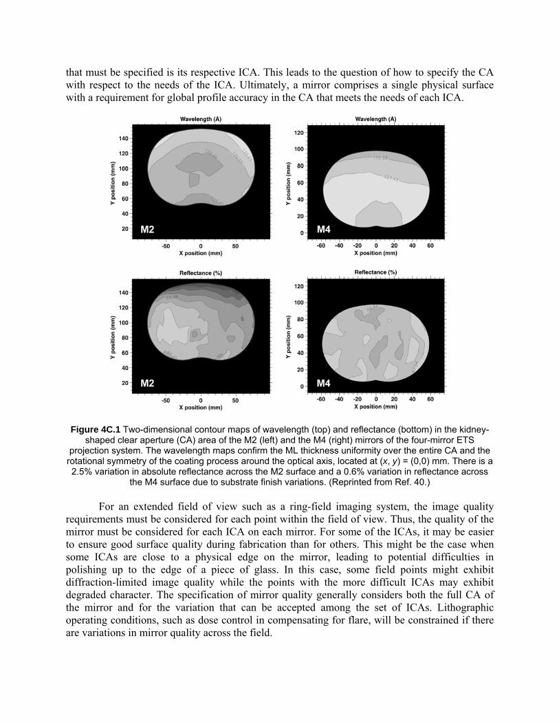
Figure 4C.1 Two-dimensional contour maps of wavelength (top) and reflectance (bottom) in the kidney-
shaped clear aperture (CA) area of the M2 (left) and the M4 (right) mirrors of the four-mirror ETS projection system. The wavelength maps confirm the ML thickness uniformity over the entire CA and the
rotational symmetry of the coating process around the optical axis, located at (x, y) = (0,0) mm. There is a 2.5% variation in absolute reflectance across the M2 surface and a 0.6% variation in reflectance across
the M4 surface due to substrate finish variations. (Reprinted from Ref. 40.) For an extended field of view such as a ring-field imaging system, the image quality requirements must be considered for each point within the field of view. Thus, the quality of the mirror must be considered for each ICA on each mirror. For some of the ICAs, it may be easier to ensure good surface quality during fabrication than for others. This might be the case when some ICAs are close to a physical edge on the mirror, leading to potential difficulties in polishing up to the edge of a piece of glass. In this case, some field points might exhibit diffraction-limited image quality while the points with the more difficult ICAs may exhibit degraded character. The specification of mirror quality generally considers both the full CA of the mirror and for the variation that can be accepted among the set of ICAs. Lithographic operating conditions, such as dose control in compensating for flare, will be constrained if there are variations in mirror quality across the field.

4C.5 Low-Frequency (Figure) Errors When considering the errors on the mirror as a function of spatial frequency, there is essentially a continuum of frequencies, each contributing to angular deviations of the rays. However, it is convenient to divide the spatial frequencies of the errors into broad categories—low, mid, and high—where each category has a qualitatively different influence on imaging performance. Low-frequency errors are considered to be those that lead to ray deflections lying approximately within the CD of the image. Thus, if the CD is 45 nm, then the delineation of the low-frequency errors on the mirror would be those that deflect the rays within a small neighborhood around the 45-nm feature. These errors determine resolution, horizontal-vertical bias, through-focus errors from coma, etc. The small slope deviations lead to fantastically small allowable height errors on the mirrors. For example, a mirror with a ripple pattern and a spatial wavelength of 1 cm located an effective distance of 0.5 m from the wafer could have a P-V (peak-to-valley) amplitude of only 0.15 nm, such that the ray deviation would be less than 45 nm. Because the ICA on any particular mirror is circular, it is possible to analyze the low-frequency errors in terms of either spatial frequency or Zernike polynomials, with essentially equivalent results. Typically, it is the first 16 to 37 Zernike terms that are used for low-frequency analysis. The advantage of using Zernike terms is the familiarity with qualitative imaging metrics, as in a statement such as “figure errors on mirror x lead to a variation in astigmatism over the field.” On the other hand, the spatial periods covered by the Zernike terms are not as neatly delineated, for example, as when low-frequency figure errors are defined as errors with a spatial period below 1 mm. The spatial frequency delineation enables one to account for all of the errors in the mirrors in terms of power spectral density (PSD); if lower-frequency errors are specified in terms of Zernike terms and higher-frequency errors specified in terms of spatial frequencies, one must be careful to avoid gaps or double-counting some frequencies in the spectrum. The practical approach to specifying low-frequency errors is to look at three important metrics: (1) the total rms power over the full CA integrated up to the frequency that scatters to the edge of the CD; (2) the total rms power within each ICA integrated to the same frequency limit, along with the variation over the set of ICAs; and (3) an analysis of key Zernike terms for each ICA and their variation over the field. By considering all of these approaches to specification, one gains a connection between the physical characteristics of the mirror, a qualitative sense of the impact on imaging performance, and often a valuable link to the method of fabrication. Although this chapter does not define acceptance criteria for each type of aberration, it is instructive to consider the relationship between specifications for the ICA and those for the full CA. For illustration, we will consider the variation of tilt over the set of ICAs and how this relates to a specification for the figure within the CA. A variation in ICA tilt aberrations across the field leads to image placement errors, or distortion. In considering tilt, which comprises Zernike terms 2 and 3 (depending on the naming convention), we have a straightforward requirement: we cannot deflect the centroid of the image of a field point by an amount determined by the distortion and image placement specification. Therefore, the tilt variation among all ICAs will be limited to an amount such that the arithmetic sum of the tilts among the corresponding ICAs on all sequential mirrors is below a maximum value. (Note the distinction between the ICAs on a single mirror and the sequential ICAs on different mirrors corresponding to a single field point.) This upper limit on tilt can be partitioned among each of the mirrors. It is reasonably straightforward to take a figure map of the mirror’s
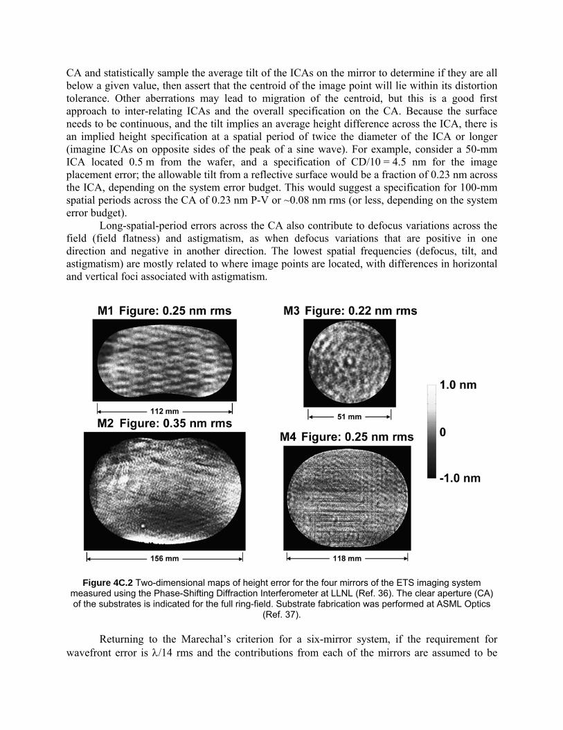
CA and statistically sample the average tilt of the ICAs on the mirror to determine if they are all below a given value, then assert that the centroid of the image point will lie within its distortion tolerance. Other aberrations may lead to migration of the centroid, but this is a good first approach to inter-relating ICAs and the overall specification on the CA. Because the surface needs to be continuous, and the tilt implies an average height difference across the ICA, there is an implied height specification at a spatial period of twice the diameter of the ICA or longer (imagine ICAs on opposite sides of the peak of a sine wave). For example, consider a 50-mm ICA located 0.5 m from the wafer, and a specification of CD/10 = 4.5 nm for the image placement error; the allowable tilt from a reflective surface would be a fraction of 0.23 nm across the ICA, depending on the system error budget. This would suggest a specification for 100-mm spatial periods across the CA of 0.23 nm P-V or ~0.08 nm rms (or less, depending on the system error budget). Long-spatial-period errors across the CA also contribute to defocus variations across the field (field flatness) and astigmatism, as when defocus variations that are positive in one direction and negative in another direction. The lowest spatial frequencies (defocus, tilt, and astigmatism) are mostly related to where image points are located, with differences in horizontal and vertical foci associated with astigmatism.
Figure 4C.2 Two-dimensional maps of height error for the four mirrors of the ETS imaging system measured using the Phase-Shifting Diffraction Interferometer at LLNL (Ref. 36). The clear aperture (CA) of the substrates is indicated for the full ring-field. Substrate fabrication was performed at ASML Optics
(Ref. 37). Returning to the Marechal’s criterion for a six-mirror system, if the requirement for wavefront error is λ/14 rms and the contributions from each of the mirrors are assumed to be

statistically independent, then each mirror is allocated a maximum wavefront error of (λ/14)/√6 = 0.029λ. The height specification is half of the wavefront for a reflective system, or about 0.015λ. For λ = 13.5 nm, the figure specification (Marechal) is 0.2 nm rms. Similarly, for a four-mirror system, the figure specification per Marechal would be about 0.25 nm rms. In Fig. 4C.2, the height errors for four mirrors of the Engineering Test Stand show that in 2000, 0.25 nm surface figure was achieved for the first demonstration of diffraction-limited performance for a full-field EUVL projection system.36,37,38 Note that the figure on substrate M2 is 0.35 nm rms instead of 0.25 nm rms. Analysis of imaging performance using the real fabrication errors indicated that this additional error resulted in uniform astigmatism across the field and would be automatically removed during system alignment, and thus did not require further correction during fabrication. As mentioned above, if other concerns such as the effective DOF of the system are taken into account, Ref. 5 suggests that the system wavefront errors may need to be limited to λ/50 rms. This is about a factor of 3 smaller than allowed by Marechal, thus suggesting that the figure errors on the mirrors should be less then 0.06-nm rms. The numerical distinction between these two sets of specifications (~0.06 versus 0.20 nm rms) is at the state of the art in mirror manufacturing (fabrication and testing). Understanding the nuances of each aspect of the specification and what determines acceptable lithographic performance (process window) is the key to the acceptance criterion. Aside from effective DOF, another concern in applying these broad “bucket-type” specifications is the assumption that the figure errors are uncorrelated among the mirrors. Six mirrors is not a large number of surfaces, and the averaging of a localized phase bump of one mirror among the other surfaces is not nearly as effective as blending errors across the dozens of surfaces for an excimer-based transmissive projection system. In fact, a more conservative approach to tolerancing certain low-order errors, such as astigmatism, would be to choose a combinatorial rule that allows some correlation among the low mode errors from different mirrors, such as astigmatic-shaped errors (the egg-shaped phase error has a chance of being co-aligned among the different mirrors). However, simulating performance with the as-fabricated errors is essential, such as in the case mentioned above where the surface errors due to uniform astigmatism across the field could be compensated during alignment. 4C.6 Mid-Spatial-Frequency Errors When ray deviation angles (or scattering angles) lead to the dose being incident on the wafer outside of the CD, the contrast of the printed features degrades. This condition is commonly referred to as flare. This broadly considers scattering angles, where the irradiance on the wafer ranges from the CD width to the edge of the printed field. If the exposure tool has a moving shutter or blades that delineate the region on the wafer exposed to light, then the range of scattering angles that contribute to flare are those that place any unwanted energy within the instantaneous exposed field. Because the distance from each mirror to the wafer is different, the spatial frequencies that contribute to flare will be different for each mirror, thus leading to a different set of specifications on each of the mirrors. In round numbers, the spatial periods that contribute to flare are often of the order of 1 µm to 1 mm. For a ring-field system, the chord length of the field is larger than the width of the ring, perhaps by 12:1, which indicates that the scattering angles that contribute to flare in the cross-field direction can extend a factor of 10 further than in the scan direction (assuming that framing blades are used to delimit the ring-field shape).
The influence of flare is to lower the contrast between the lines and spaces, leading to a decreased exposure-defocus (E-D) process window. Flare can also be analyzed by PSF broadening, which has been described as the addition of a skirt around the core of the intensity peak.7 Essentially all effects that redistribute energy from the peak of the PSF to the skirt have an influence on flare by decreasing the Strehl ratio. The finite size of the CD distinguishes mid-spatial-frequency errors from figure errors for longer spatial periods, and the finite field of view delimits the effect of mid-spatial-frequency errors from wide-angle scattering for short spatial periods. Gullikson8,9 analyzed mid-spatial-frequency errors from developmental EUV mirrors and estimated the level of flare for projection optical systems with differing numbers of mirrors, as is illustrated in Fig. 4C.3 from Ref. 10. It has been shown that the influence of flare on lithographic printing can be approximated as a convolution between a flare PSF and the printed image.11
(a) (b)
Figure 4C.3 (a) Flare calculations versus substrate roughness are shown for a full-field, 0.1 numerical
aperture (NA), four-mirror camera (the Engineering Test Stand, ETS), and for a microfield, 0.3-NA, two-mirror camera (the Micro-Exposure Tool, MET). The solid points are calculations derived from actually fabricated and measured substrate sets. A calculation of the flare for a six-mirror EUVL camera is also
shown as dash line (b) Spatial frequencies relevant to flare for each of the four mirrors in the ETS camera. (Reprinted from Ref. 10 courtesy of E. M. Gullikson at LBNL.)
4C.7 High-Spatial-Frequency Errors When the scattering angle is sufficiently large to direct light outside of the image field, it leads to an energy loss, i.e. low dose. The specific spatial periods of roughness that contribute to wide-angle scattering are unique to each mirror. In general, high-spatial-frequency roughness (MSFR) is most often characterized using an atomic force microscope (AFM), an example of which is shown in Fig. 4C.4. MSFR might be superficially delimited as spatial periods less than 1 µm, although there may be a difference factor of 10 in the spatial period that defines wide-angle
scattering among the mirrors. There may be a factor of 12 difference in spatial periods that define the low-spatial-frequency boundary in the scan and cross-scan directions. High-spatial-frequency roughness (HSFR) variations across a substrate CA will lead to commensurate variations in reflectivity from the ML-coated mirror. If such variation is sufficiently large, it will lead to apodization effects across the system exit pupil and will ultimately result in poor CD uniformity across the printed field, as was discussed in Sec. 4C.2. Figure 4C.1 from Ref. 40 provides an example of reflectance nonuniformity due to substrate finish across actual ML-coated EUVL mirrors.
Figure 4C.4 AFM measurements performed at LLNL on two Zerodur substrates designed for imaging at
EUV wavelengths. On the left, the two AFM images contain superimposed polishing marks, in preferential and random directions on the surface, and are attributed to a conventional polishing process. On the
right, the two AFM images show uniform and isotropic surface topography with granular appearance and a shoulder-like feature in the PSD curve, which are attributed to an ion-beam polishing process.
(Reprinted from Ref. 25.) 4C.8 Influence of Coatings on Roughness Specification All of the mirrors will have a ML coating deposited upon them. Stearns has modeled the film growth and evolution of substrate roughness during the ML deposition process, and how this relates to scattering.12 Broadly speaking, for the high-quality coatings that have been deposited for EUVL applications, there will be some smoothing due to the deposition process. This is distinctly different from coating processes that lead to “cauliflower” growth, or the intentional deposition of columnar structures for photonics applications.13 For the DC-magnetron coatings familiar to the authors, a smoothing effect begins for spatial periods shorter than about 50 nm. This smoothing might be characterized as a transfer function where periods smaller than 50 nm are attenuated and periods longer than 50 nm are replicated throughout the coating. The filtering effect is important in estimating the predicted loss from a surface, and in setting an upper limit on spatial frequency for specifying the HSFR for the substrate fabricator. It has been shown that

the smoothing effect of the coating can be extended to longer spatial periods (>1 µm) for ion-beam deposition, particularly if an intermediate ion etching process is incorporated into the process.14
4C.9 Calculation of Surface Errors Except for the consideration of specific Zernike terms, the useful metric for describing surface height errors is the 2D PSD. The formalism for calculating the 2D PSD is described by Taylor, where the output is a 2D image in frequency space delineated by spatial frequency in the x and y directions, respectively.15 The units of the 2D PSD are length to the 4thpower. Analysis of these frequency-space plots can be useful, especially in searching for specific directional periodicities. In the case of roughness, it is often useful to calculate the average radial PSD, which is determined by selecting a broad set of traces from the 2D plot beginning at the origin, where each trace is directed in a different direction. The set of radial 2D PSDs are then averaged and plotted as a single curve versus spatial frequency; the units are still length to the 4th power. The value of this representation is that tendencies for periodicities are graphically discernable, and that PSDs may be more readily compared. For example, it is often convenient to compare PSDs from different mirrors or different vendors, or to track a mirror as it progresses through various polishing or coating operations. From the average radial PSD, one can observe whether the coating operation has had a smoothing effect on the higher spatial frequencies. The radial PSD should only be considered if there is a reason to assume that the height errors encompassed by the spatial frequency range of the calculation are isotropic. It is necessary to build up a broad-spectrum PSD from the overlapping PSDs of many measurements, spanning different instruments and instrument bandwidths. The PSD from each instrument will show some evidence of its intrinsic transfer function and will generally have a range that is representative of the surface and not dominated by instrument roll-off. It is often useful to fit a high-order polynomial (e.g., 6th order) to the PSD for a simplified representation of the errors, or to consider a fractal fit. Note that a 1D PSD is not a single trace from a 2D PSD, but is related to the 2D PSD by an integral transform.16
4C.10 Uniformity The goals of constructing an optical system include meeting a minimal level of wavefront control and distortion for all points within the ring-field. Variations in optical quality across the ring-field also should be minimized, because they affect the variations in the E-D window across the field. For example, variations in flare across the field tend to change the contrast and the exposure demands to clear the resist across the field. In deep ultraviolet (DUV) systems, some flare variations are predictable and could be considered in the mask design. For EUV systems, flare variations will generally be dominated by variations in polishing quality across the field, which should be minimized. Variations in HSFR lead to nonuniform pupil illumination, resulting in anomalies in spatial coherence and weighting of the pupil aberrations. As an example, some nonuniformity in the effective pupil illumination due to variations in wide-angle scattering could result in a horizontal-vertical printing bias. The flare variation across the field for EUV imaging systems is potentially much less than for DUV imaging systems, with significant roll-off only at the edge of the field.17
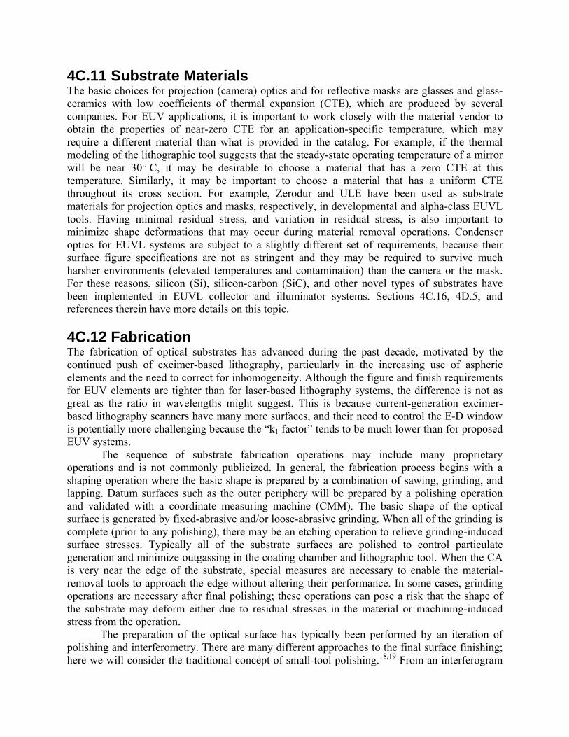
4C.11 Substrate Materials The basic choices for projection (camera) optics and for reflective masks are glasses and glass-ceramics with low coefficients of thermal expansion (CTE), which are produced by several companies. For EUV applications, it is important to work closely with the material vendor to obtain the properties of near-zero CTE for an application-specific temperature, which may require a different material than what is provided in the catalog. For example, if the thermal modeling of the lithographic tool suggests that the steady-state operating temperature of a mirror will be near 30° C, it may be desirable to choose a material that has a zero CTE at this temperature. Similarly, it may be important to choose a material that has a uniform CTE throughout its cross section. For example, Zerodur and ULE have been used as substrate materials for projection optics and masks, respectively, in developmental and alpha-class EUVL tools. Having minimal residual stress, and variation in residual stress, is also important to minimize shape deformations that may occur during material removal operations. Condenser optics for EUVL systems are subject to a slightly different set of requirements, because their surface figure specifications are not as stringent and they may be required to survive much harsher environments (elevated temperatures and contamination) than the camera or the mask. For these reasons, silicon (Si), silicon-carbon (SiC), and other novel types of substrates have been implemented in EUVL collector and illuminator systems. Sections 4C.16, 4D.5, and references therein have more details on this topic. 4C.12 Fabrication The fabrication of optical substrates has advanced during the past decade, motivated by the continued push of excimer-based lithography, particularly in the increasing use of aspheric elements and the need to correct for inhomogeneity. Although the figure and finish requirements for EUV elements are tighter than for laser-based lithography systems, the difference is not as great as the ratio in wavelengths might suggest. This is because current-generation excimer-based lithography scanners have many more surfaces, and their need to control the E-D window is potentially more challenging because the “k1 factor” tends to be much lower than for proposed EUV systems. The sequence of substrate fabrication operations may include many proprietary operations and is not commonly publicized. In general, the fabrication process begins with a shaping operation where the basic shape is prepared by a combination of sawing, grinding, and lapping. Datum surfaces such as the outer periphery will be prepared by a polishing operation and validated with a coordinate measuring machine (CMM). The basic shape of the optical surface is generated by fixed-abrasive and/or loose-abrasive grinding. When all of the grinding is complete (prior to any polishing), there may be an etching operation to relieve grinding-induced surface stresses. Typically all of the substrate surfaces are polished to control particulate generation and minimize outgassing in the coating chamber and lithographic tool. When the CA is very near the edge of the substrate, special measures are necessary to enable the material-removal tools to approach the edge without altering their performance. In some cases, grinding operations are necessary after final polishing; these operations can pose a risk that the shape of the substrate may deform either due to residual stresses in the material or machining-induced stress from the operation. The preparation of the optical surface has typically been performed by an iteration of polishing and interferometry. There are many different approaches to the final surface finishing; here we will consider the traditional concept of small-tool polishing.18,19 From an interferogram

of the surface, a map of the height errors on the surface is generated within the coordinate system defined by the data. The polishing tool will have a characteristic removal footprint, which might qualitatively be envisioned as Gaussian, although vastly different shapes are possible. The amount of material that is removed is a function of how long the tool dwells in a location, or analogously, how slowly it laterally scans over the optic. The amount of material that is removed from any one point on the surface is due to the sum of the contributions from all positions of the polishing tool. A deconvolution routine determines the appropriate scan speeds or dwell times as the tool traverses over the surface. For a given tool and set of errors, only a fraction of the errors will be removed in one iteration. As the height of the errors decreases to the process control limits and the repeatability level of the interferometry, the convergence will become less deterministic. At this ragged edge of technology, meeting the leading-edge specifications will stress the equipment, data analysis, and procedural discipline of the team. Note that other methods for the finishing of optics include magneto-rheological finishing20 and ion-beam figuring.21-24 Figure 4C.2 illustrates the residual low-frequency errors on Zerodur EUVL substrates for the ETS36,37 and Figure 4C.3 shows an example of the morphology in the high-spatial-frequency range, as measured by AFM at Lawrence Livermore National Laboratory (LLNL), for two Zerodur EUV optical substrates polished by two different techniques (from Ref. 25). Often during the final convergence phases on figure and finish specifications, a tradeoff develops between figure correction and polishing to achieve an acceptable surface finish.26. This tradeoff is best exemplified by considering a plot of the average radial PSD. Figuring tools tend to conform to the optical surface and achieve their desired removal by dwelling at a given location for a specified period of time (usually accomplished by a variation in scan speed). Tools for improving finish tend to have a stiff surface, and they remove material by bridging across the roughness and preferentially removing the high spots. The art of designing a polishing process is to have tools that fulfill both of these requirements, or separate tools with characteristics that do not overlap into each other’s spatial frequency domain (e.g., a figuring tool that does not address finish, and a smoothing tool that does not affect figure). In reality, this separation between figure and finish does not perfectly occur, and switching between tools tends to degrade the PSD in the zone of overlap. When tracking the convergence of meeting a specification on a PSD plot, one sees the PSD tilt down to the left when improving figure, and tilt up on the right while degrading finish. The converse can be observed when the finish tool is used. The point at which the PSD tilts (i.e., the fulcrum) is often around a spatial period of 1 mm. Successful polishing operations will minimize the amount of degradation that occurs for spatial periods other than the one being purposefully addressed while sequentially lowering the fulcrum point with each iteration. 4C.13 Metrology As discussed above in terms of specifications, all of the spatial frequencies of the height errors on the substrate affect the performance of the optical system. Therefore, metrology covering the full spectrum of spatial frequencies is necessary to aid in fabrication, validate specifications, and provide substrate data to simulate the performance of the optical system. For figure errors, the most common means of obtaining height data is interferometry (often phase-shifting), where the aperture of the measurement can range from portions of the CA or ICAs, to the full CA. The mirrors are typically aspheric, which usually results in the fringes being very closely spaced in the regions of high aspheric slope. This condition will require either the use of null compensators,27 or high-resolution cameras to resolve high fringe density, or the adoption of

stitching methods to link multiple height maps from subregions on the surface.28,29 The measurement of aspheric optical surfaces poses numerous challenges in controlling measurement errors, although detailed approaches to understanding measurement errors have been presented.30-34 In prototype EUVL systems (see Fig 4C.2), interferometric measurements have been made using the phase-shifting diffraction interferometer (PSDI)35 that support the determination of figure errors (spatial periods ranging from the full CA to 1 mm) with an accuracy of less than 0.25 nm rms.36,37,38 In the case referred to in Ref. 35, the estimated accuracy for the interferometric measurement was consistent with the measured wavefront error of the aligned optical system. In another case, some small discrepancies were found between independent interferometric measurements of the same mirror, possibly due to systematic errors in one of the systems.39 For MSFR, the relevant spatial frequencies include the high-spatial-frequency portion of the range measured by large-aperture interferometry, the range covered by phase-measuring microscopy (PMM), and often the low-frequency portion of the range covered by an AFM instrument. The specifics of the mid-frequency range depend on the factors mentioned regarding specifications, although this can nominally include periods of 1 mm to 1 µm, which corresponds to the bandwidth typically covered by PMMs. As the mid-frequency roughness of a high-quality lithographic mirror may be about 0.1- to 0.2-nm rms, this may be comparable or better than the roughness of many reference mirrors used in PMMs. Although these reference mirrors can be specially fabricated to a lower roughness (with significant difficulty), the usual procedure is to calibrate the reference mirror by a multiple-measurement averaging process. For aspheric surfaces, care must be taken to repeat the calibration when moving to regions of different curvature or when the fringe pattern is adjusted to ensure that the appropriate region of the reference mirror is used. AFM is typically required to measure HSFR, because the spatial periods are typically less than 1 µm. Due to the smoothing tendency of ML deposition, the smallest periods normally needed for measurement are 20 to 50 nm. Without this smoothing tendency, characterization to smaller periods would be needed where the band limit of the measurement was approximately the tip radius of the stylus (~5 nm), with some extension using deconvolution techniques. The quality of the AFM measurement is highly dependent on the methodology employed by the microscopist, such as in the selection of styli, the frequency of changing tips to account for wear, control of electrostatic charge, and care in minimizing background vibration. At LLNL, the AFM used to measure EUVL optics has a background signal noise of about 0.03 nm rms.25 Of particular importance in the use of the AFM is the interpretation of the micrographs. Residual contamination of the surface due to solvent residue or polishing compound can be identified, especially when working closely with vendors or technicians, and a familiarity with cleaning capabilities and fabrication methods can develop. Often, significant differences have existed in the measured rms roughness between LLNL AFM results and those of other organizations. At LLNL, the surface finish metrology is often compared with angle-resolved scattering measurements by the Advanced Light Source (ALS) at Lawrence Berkeley National Lab (LBNL) to continually validate the relationship between profile metrology and functional performance.40,41
4C.14 Mounting and Assembly The support of the optical elements is of extreme importance. The method of support must not induce unexpected changes in the figure, must not be overly sensitive to thermal changes or
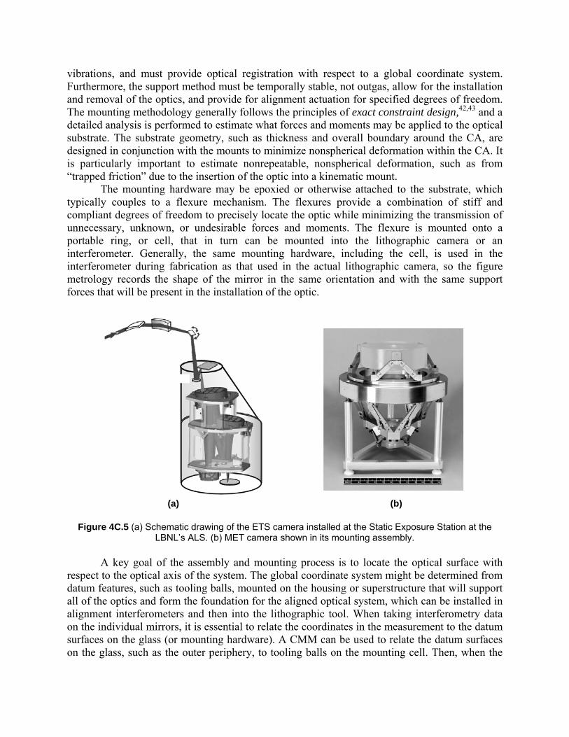
vibrations, and must provide optical registration with respect to a global coordinate system. Furthermore, the support method must be temporally stable, not outgas, allow for the installation and removal of the optics, and provide for alignment actuation for specified degrees of freedom. The mounting methodology generally follows the principles of exact constraint design,42,43 and a detailed analysis is performed to estimate what forces and moments may be applied to the optical substrate. The substrate geometry, such as thickness and overall boundary around the CA, are designed in conjunction with the mounts to minimize nonspherical deformation within the CA. It is particularly important to estimate nonrepeatable, nonspherical deformation, such as from “trapped friction” due to the insertion of the optic into a kinematic mount. The mounting hardware may be epoxied or otherwise attached to the substrate, which typically couples to a flexure mechanism. The flexures provide a combination of stiff and compliant degrees of freedom to precisely locate the optic while minimizing the transmission of unnecessary, unknown, or undesirable forces and moments. The flexure is mounted onto a portable ring, or cell, that in turn can be mounted into the lithographic camera or an interferometer. Generally, the same mounting hardware, including the cell, is used in the interferometer during fabrication as that used in the actual lithographic camera, so the figure metrology records the shape of the mirror in the same orientation and with the same support forces that will be present in the installation of the optic.
(a) (b)
Figure 4C.5 (a) Schematic drawing of the ETS camera installed at the Static Exposure Station at the
LBNL’s ALS. (b) MET camera shown in its mounting assembly. A key goal of the assembly and mounting process is to locate the optical surface with respect to the optical axis of the system. The global coordinate system might be determined from datum features, such as tooling balls, mounted on the housing or superstructure that will support all of the optics and form the foundation for the aligned optical system, which can be installed in alignment interferometers and then into the lithographic tool. When taking interferometry data on the individual mirrors, it is essential to relate the coordinates in the measurement to the datum surfaces on the glass (or mounting hardware). A CMM can be used to relate the datum surfaces on the glass, such as the outer periphery, to tooling balls on the mounting cell. Then, when the

mounting cell is installed into the housing, the CMM can be used to relate the tooling balls on the cell to the global coordinate system defined by the datum surfaces on the housing. So the chain of steps in registering the optic to the housing includes: (1) relate the interferogram (height map) to datum features on the edge of the mirror; (2) relate the mirror datums to datums (tooling balls) on the cell; (3) relate the datums on the cell (tooling balls) to datums on the housing. At the completion of this assembly process, the coordinates for each mirror will be known with respect to the global coordinate system. The inter-relationships among the mirrors can then be determined. By rigorously documenting the uncertainty in locating all of the datum surfaces, the uncertainty in locating the optics relative to one another can be estimated. It has been demonstrated that the mechanical assembly of a four-mirror EUVL projection system, without adjustment, could achieve a 5-nm rms wavefront.36 Figure 4C.5 illustrates two examples of the mounting schemes implemented for the Engineering Test Stand (ETS) four-mirror, full-field projection system, and the microexposure tool (MET) two-mirror microfield system. 4C.15 Alignment A rigorous procedure for aligning EUVL optical systems has been developed where the influence of rigid body positional errors on the optical system were calculated in terms of Zernike polynomials.44 In many cases, similar influences on the system aberrations could be obtained with different choices in optics adjustments. An analysis using singular value decomposition was employed to determine the sensitivities of system performance to the alignment motions and to determine the optimal adjustments for optimizing performance with a given starting set of aberrations. The analysis can be performed initially using the sensitivities determined from the optical design code using the ideal mirror shapes; however, inserting the as-built mirror metrology data into the analysis will account for substrate aberrations. The sensitivities can be measured experimentally by using an alignment interferometer and measuring the change in system aberrations with small actuations of the mirrors. This would be performed for multiple field points within the ring-field. When performing system alignment, wavefront errors and distortion must be measured at numerous points within the ring-field. A phase-shifting point-diffraction interferometer (PSPDI) has been developed for alignment that has achieved an absolute accuracy of less than 0.20-nm rms.45,46 Essentially, a calibrated, nearly-perfect spherical wave (i.e., the “test wave”) is propagated from one of the system’s field points to its conjugate point, where it is combined with a nearly-perfect reference wave. The wave that passes through the optical system becomes aberrated due to design residuals, fabrication errors, and alignment errors. The test wave and the reference wave interfere and are interpreted to determine the system aberrations. The locations of the points where the test and reference waves are launched are varied over the full ring-field to determine the full-field performance. The measured tilt aberrations can be related to distortion. The combination of wavefront error and distortion data over the full set of field points can be used to optimize the mirror alignment. Generally, the average performance over the field will be optimized such that all points meet a minimally acceptable criterion or process window. 4C.16 Condenser Optics The requirements for condenser optics are significantly different than for projection optics. The condenser’s basic requirement is to direct EUV illumination onto the mask and through the pupil of the camera. For a Köhler condenser, the general goal is to image the source onto the pupil of the projection system. The condenser does not need to be diffraction-limited because its goal is
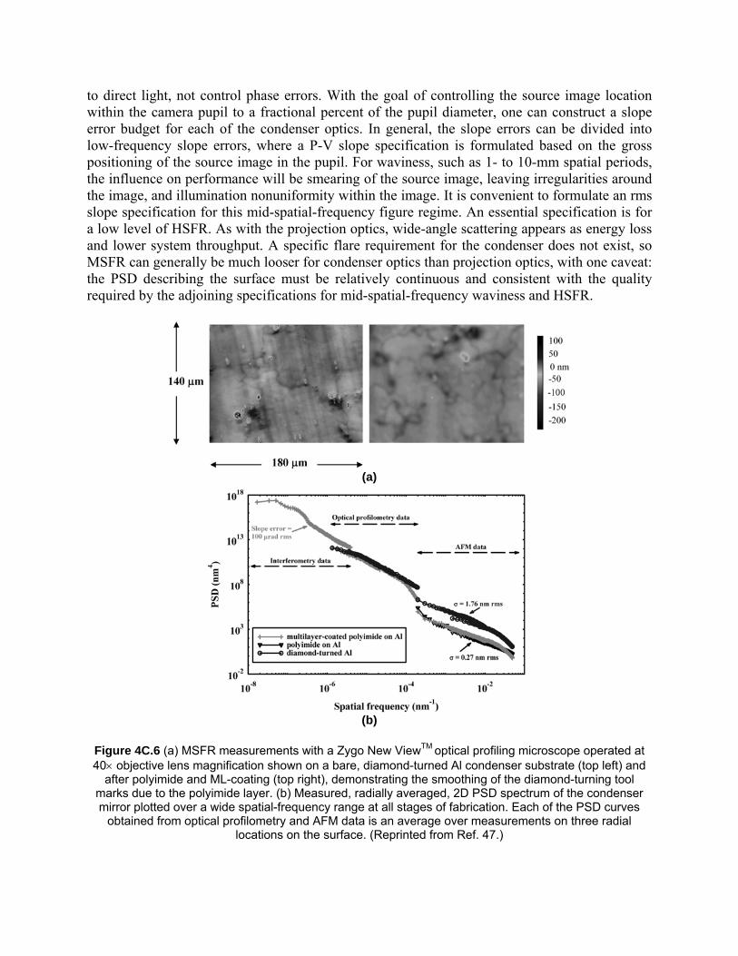
to direct light, not control phase errors. With the goal of controlling the source image location within the camera pupil to a fractional percent of the pupil diameter, one can construct a slope error budget for each of the condenser optics. In general, the slope errors can be divided into low-frequency slope errors, where a P-V slope specification is formulated based on the gross positioning of the source image in the pupil. For waviness, such as 1- to 10-mm spatial periods, the influence on performance will be smearing of the source image, leaving irregularities around the image, and illumination nonuniformity within the image. It is convenient to formulate an rms slope specification for this mid-spatial-frequency figure regime. An essential specification is for a low level of HSFR. As with the projection optics, wide-angle scattering appears as energy loss and lower system throughput. A specific flare requirement for the condenser does not exist, so MSFR can generally be much looser for condenser optics than projection optics, with one caveat: the PSD describing the surface must be relatively continuous and consistent with the quality required by the adjoining specifications for mid-spatial-frequency waviness and HSFR.
(a)
(b)
Figure 4C.6 (a) MSFR measurements with a Zygo New ViewTM optical profiling microscope operated at 40× objective lens magnification shown on a bare, diamond-turned Al condenser substrate (top left) and
after polyimide and ML-coating (top right), demonstrating the smoothing of the diamond-turning tool marks due to the polyimide layer. (b) Measured, radially averaged, 2D PSD spectrum of the condenser mirror plotted over a wide spatial-frequency range at all stages of fabrication. Each of the PSD curves
obtained from optical profilometry and AFM data is an average over measurements on three radial locations on the surface. (Reprinted from Ref. 47.)
An important area of development for condenser optics is in lowering the cost of the elements, especially the collector, whose degradation is expected to be faster than that of the projection optics. Novel approaches have been developed to smooth HSFR by applying either a polyimide,47,48 as illustrated in Fig. 4C.6, or spin-on glass coatings.49 These applied coatings will smooth the HSFR, with the goal to not significantly degrade the slope errors at the longer spatial periods. Promising results have been presented for the polyimide smoothing of diamond-turned aluminum (Al) substrates47 and ground SiC substrates,48 and the spin-on-glass smoothing of Al and copper (Cu) diamond-turned substrates.49 These results show that high reflectance is obtained when a ML coating is applied on top of the smoothing layer, and that the smoothing layer is temporally stable and does not outgas. Acknowledgements The authors gratefully acknowledge the EUV LLC and SEMATECH for their support of EUVL programs at the Lawrence Berkeley, Lawrence Livermore, and Sandia National Laboratories (LBNL, LLNL, and SNL). References
1. R. Hudyma, “An overview of optical systems for 30 nm resolution lithography at EUV wavelengths,” Proc. SPIE 4832, 137–148 (2002).
2. For example, see D. G. Flagello, J. de Klerk, G. Davies, et al., “Towards a comprehensive control of full-field image quality in optical photolithography,” Proc. SPIE 3051, 672–685 (1997).
3. F. Zernike, “Beugungstheorie des Schneidenverfahrens und seiner verbesserten Form, der Phasenkontrastmethode,” Physica 1, 689–704 (1934).
4. J. C. Wyant and K. Creath, “Basic wavefront aberration theory for optical metrology,” in Applied Optics and Optical Engineering, Volume XI, Academic Press, New York, pp. 1–53 (1992).
5. D. M. Williamson, “The elusive diffraction limit,” in Extreme Ultraviolet Lithography, F. Zernike and D. T. Attwood, Eds., OSA Proc. 23, 68–76 (1994).
6. See Ref. 2 for a discussion of bananicity. 7. J. E. Harvey, W. Zmek, and C. Ftaklas, “Imaging capabilities of normal-incidence x-ray
telescopes,” Opt. Eng. 29(6), 603–608 (1990). The reader is also referred to papers by E. Church, P. Takacs, and J. Bennett.
8. E. M. Gullikson, “Scattering from normal incidence EUV optics,” Proc. SPIE 3331, 72–80 (1998).
9. E. M. Gullikson, S. L. Baker, J. E. Bjorkholm, et al., “EUV scattering and flare of 10x projection cameras,” Proc. SPIE 3676, 717–723 (1999).
10. E. M. Gullikson, “Development of reflective EUV and soft x-ray optics,” presented at the 2nd International Symposium on Technologies and Applications of Photoelectron Micro-Spectroscopy with Laser-Based VUV Sources, Tsukuba, Japan, Feb. 1–3, 2005.
11. M. Chandhok,, S. H. Lee, C. Krautschik, et al., “Comparison of techniques to measure the point spread function due to scatter and flare in EUV lithography systems,” Proc. SPIE 5374, 854–860 (2004).
12. D. G. Stearns, “Stochastic model for thin film growth and erosion,” Appl. Phys. Lett. 62, 1745–1747 (1993).
13. Lakhtakia and R. Messier, Sculptured Thin Films: Nanoengineered Morphology and Optics, SPIE Press, Bellingham, WA (2005).
14. E. Spiller, S. L. Baker, P. B. Mirkarimi, et al., “High-performance Mo-Si multilayer coatings for extreme ultraviolet lithography,” Appl. Opt. 42, 4049–4058 (2003).
15. J. S. Taylor, G. E. Sommargren, D. W. Sweeney, and R. M. Hudyma, “The fabrication and testing of optics for EUV projection lithography,” Proc. SPIE 3331, 580–590 (1998).
16. E. L. Church and P. Z. Takacs, “Specification of the Figure and Finish of EUV mirrors in terms of performance requirements,”in Extreme Ultraviolet Lithography, F. Zernike and D. T. Attwood, Eds., OSA Proc. 23, 77–82 (1994).
17. S. H. Lee, M. Chandhok, C. Krautschik, and M. Goldstein, “Anisotropic EUV flare measured in the Engineering Test Stand (ETS),” Proc. SPIE 5374, 818–823 (2004).
18. J. S. Taylor, M. Piscotty, A. Lindquist, Eds., Fabrication and Testing of Aspheres, Trends in Optics and Photonics (TOPS) Vol. XXIV, Optical Society of America, Washington D.C. (1999).
19. R. A. Jones, Ed., Selected Papers on Computer Controlled Optical Surfacing, Vol. MS40, SPIE Press, Bellingham, WA (1991).
20. D. Golini, “Precision optics manufacturing using magnetorheological finishing,” Proc. SPIE 3739, 78–85 (1999).
21. F. Frost, R. Fechner, B. Ziberi, D. Flamm, and A. Schindler, “Large area smoothing of optical surfaces by low-energy ion beams,” Thin Solid Films 459, 100–105 (2004).
22. L. N. Allen and R. E. Keim, “An ion figuring system for large optics fabrication,” Proc. SPIE 1168, 33–50 (1989).
23. R. Geyl and E. Rolland, “Large optics ion figuring,” Proc. SPIE 3739, 161–166 (1999). 24. P. Kürz, “Optics for EUV lithography,” presented at the 2nd International Workshop on
EUV Lithography, Burlingame, CA, Oct. 17–19, 2000, sponsored by SEMATECH. 25. R. Soufli, S. L. Baker, D. L. Windt, et al., “Atomic force microscopy characterization of
Zerodur mirror substrates for the extreme ultraviolet telescopes aboard NASA’s Solar Dynamics Observatory,” Appl. Opt. 46, 3156–3163 (2007).
26. U. Dinger, G. Seitz, S. Schulte, et al., “Fabrication and metrology of diffraction-limited soft x-ray optics for the EUV microlithography,” Proc. SPIE 5193, 18–28 (2004).
27. D. Shafer, “Null lens design techniques,” Appl. Opt. 31(13), 2184–2187 (1992). 28. M. Bray, “Stitching interferometry: Side effects and PSD,” Proc. SPIE 3782, 443–452
(1999). 29. J. Fleig, P. Dumas, P. E. Murphy, and G. W. Forbes, “An automated subaperture stitching
interferometer workstation for spherical and aspherical surfaces,” Proc SPIE 5188, 296–307 (2003).
30. G. E. Sommargren, D. W. Phillion, M. A. Johnson, N. Q. Nguyen, A. Barty, F. J. Snell, D. R. Dillon, L. S. Bradsher, “100-picometer interferometry for EUVL”, Proc. SPIE 4688 316-328 (2002).
31. D. Phillion, “General methods for generating phase shifting interferometry algorithms,” Appl. Opt. 37(3), 8098–8115 (1997).
32. S. M. Arnold and R. Kestner, “Verification and certification of CGH aspheric nulls,” Proc. SPIE 2536, 117–126 (1995).
33. L. A. Selberg, “Interferometry accuracy and precision,” Proc. SPIE 1400, 24–32 (1990). 34. C. J. Evans, “Absolute figure metrology of high precision optical surfaces,” PhD thesis,
The Univ. of Birmingham, June 1996.
35. G. E. Sommargren, “Phase shifting diffraction interferometry for measuring extreme ultraviolet optics,” in Extreme Ultraviolet Lithography, G. Kubiak and D. Kania, Eds., OSA Trends in Optics and Photonics (TOPS) Vol. 4, pp. 108–112 (1996).
36. J. S. Taylor, “Construction of the projection optics box for the Engineering Test Stand,” presented at the 2nd International Workshop on EUV Lithography, Burlingame, CA, Oct. 17–19, 2000, sponsored by SEMATECH.
37. L. Marchetti, D. Bajuk, J. Kennon, et al., “Fabrication of the ETS Set II optics: Results and future development,” presented at the 2nd International Workshop on EUV Lithography, Burlingame, CA, Oct. 17–19, 2000, sponsored by SEMATECH.
38. D. A. Tichenor et al., “System integration and performance of the EUV Engineering Test Stand,” Proc. SPIE 4343, 19–37 (2001).
39. J. S. Taylor, G. Sommargren, R. Soufli, et al., “Fabrication and metrology of the high-NA imaging optics for the micro-exposure tool (MET),” presented at the 3rd International Workshop on EUV Lithography, Matsue, Japan, Oct. 29–31, 2001, sponsored by SEMATECH.
40. R. Soufli, E. Spiller, M. A. Schmidt, et al., “Multilayer optics for an extreme ultraviolet lithography tool with 70 nm resolution,” Proc. SPIE 4343, 51–59 (2001).
41. R. Soufli, R. M. Hudyma, E. Spiller, et al., “Sub-diffraction-limited multilayer coatings for the 0.3 numerical aperture micro-exposure tool for extreme ultraviolet lithography,” Appl. Opt. 46, 3736–3746 (2007).
42. L. C. Hale, “Principles and techniques for designing precision machines,” PhD thesis, Massachusetts Institute of Technology (1999).
43. D. L. Blanding, Exact Constraint: Machine Design Using Kinematic Processing, American Society of Mechanical Engineers, New York (1999).
44. H. N. Chapman and D. W. Sweeney, “A rigorous method for compensation selection and alignment of microlithographic optical systems,” Proc. SPIE 3331, 102–113 (1998).
45. D. W. Phillion, G. E. Sommargren, M. A. Johnson, et al., “Calibration of symmetric and non-symmetric errors for interferometry of ultra-precise imaging systems,” Proc. SPIE 5869, 5869OR (2005).
46. M. A. Johnson, D. W. Phillion, G. E. Sommargren, et al., “Construction and testing of wavefront reference sources for interferometry of ultra-precise imaging systems,” Proc. SPIE 5869, 5869OP (2005).
47. R. Soufli, E. Spiller, M. A. Schmidt, et al., “Smoothing of diamond-turned substrates for extreme-ultraviolet illuminators,” Opt. Eng. 43(12), 3089–3095 (2004).
48. R. Soufli, S. L. Baker, S. Ratti, et al., “Substrate smoothing for high-temperature condenser operation in EUVL source environments,” Proc. SPIE 5751, 140–145 (2005).
49. F. Salmassi, P. P. Naulleau, and E.M. Gullikson, “Spin-on-glass coatings for the generation of superposihed substrates for use in the extreme-ultraviolet region,” Appl. Opt. 45, 2404–2408 (2004).
Chapter 4D
Multilayer Coatings for EUVL
Regina Soufli and Saša Bajt
Contents 4D.1 Overview and History of EUV Multilayer Coatings....................................................... 47 4D.2 Choice of ML Materials and Wavelength Considerations ............................................. 47 4D.3 Multilayer Deposition Technologies ................................................................................. 48 4D.4 Theoretical design .............................................................................................................. 49 4D.5 High Reflectivity, Low Stress, and Thermal Stability Considerations ......................... 50 4D.6 Optical Constants............................................................................................................... 51 4D.7 Multilayer Thickness Specifications for Imaging and Condenser EUVL Mirrors...... 52 Acknowledgements ..................................................................................................................... 55 References.................................................................................................................................... 55

4D.1 Overview and History of EUV Multilayer Coatings Highly reflective multilayer (ML) coatings deposited on precisely polished mirror substrates have enabled imaging at EUV and x-ray wavelengths at near-normal angles of incidence. These ML films essentially represent synthetic Bragg crystals made of alternating layers of materials, where the constructive interference of light between the layers results in significant reflectivity at normal incidence. Stable interfaces and sufficient contrast in the refractive index between the material layers are the most fundamental requirements for these ML structures to function efficiently. The first attempt in 1940 by DuMond and Youtz1 to make copper-gold (Cu-Au) MLs resulted in the loss of reflective performance after a few days due to interdiffusion between the layers. However, Dinklage2 in 1967 and Spiller3 in 1972 were the first to make successful experimental demonstrations of ML films with stable reflective performance over time, operating at EUV/x-ray wavelengths, followed by T. Barbee4 and J. Underwood.5 In the following two decades, significant activity occurred in this direction by the groups at Bell Laboratories and at Lawrence Berkeley, Lawrence Livermore, and Sandia National Laboratories (LBNL, LLNL, and SNL) in the U.S., and NTT Laboratories in Japan. These early efforts were motivated by the need for ML mirrors for EUV/x-ray solar physics, EUV/x-ray lithography6 x-ray microscopy, and x-ray lasers for defense applications. These researchers established the vacuum-deposition techniques and general principles of making such ML structures into practical elements for EUV and x-ray instrumentation. The rapid advancement of laser-produced plasma (LPP) source EUV reflectometers7-9 and second- and third-generation synchrotron facilities10 that occurred at about the same time made possible the accurate and reproducible at-wavelength characterization of ML films, thus further accelerating the development of ML technology. 4D.2 Choice of ML Materials and Wavelength Considerations The illumination wavelength of 13.5 nm was chosen for EUV lithography (EUVL) based on the early development and good performance of molybdenum-silicon (Mo-Si) MLs in this wavelength region. Mo-Si still remains the most extensively investigated and best understood ML material pair to date, and 13.5 nm is in the wavelength region just longer than the L2,3 absorption edge of Si (12.4 nm), where Mo/Si achieves its best reflective performance. In addition, the first available sources for EUVL were LPP sources, with good conversion efficiency in this wavelength region. The earliest optical systems constructed to demonstrate printing capabilities at EUV wavelengths were 10X Schwartzchild cameras (microsteppers) at 13.4 nm, using Mo-Si coated mirrors11 At around the same time, a new class of beryllium (Be) based MLs was developed, including Mo-Be, ruthenium (Ru-Be), rhenium (Rh-Be), and niobium (Nb-Be).12,13 The aim of this development was to explore the potential of the wavelength region just longer than the Be K edge (11.12 nm) for EUVL. Mo/Be MLs with measured reflectivity approaching 70% were demonstrated at 11.3 nm, the highest experimental reflectivity achieved at any EUV wavelength at that time.14 Adding to the appeal of the 11-nm wavelength was the fact that the potential LPP EUVL sources had spectra with higher output at 10 to 11 nm, and the shorter wavelength allowed for photoresist layers with higher thickness and fewer defects. For these reasons, Mo-Be was seriously considered as a candidate ML pair for EUVL optics, and was later revisited and further optimized.15,16 MoRu/Be MLs were also demonstrated17 at wavelengths around 11 nm and had the additional advantage of MoRu’s amorphous layer structure (versus the crystalline structure in both Mo and Be layers in Mo/Be MLs), which are amenable to smoothing for both EUVL optics and masks. Nevertheless, in 1999–2000 the international semiconductor community abandoned Be-based MLs and the 11-nm wavelength
region for EUVL, mainly due to health and safety issues associated with the toxicity of Be particles. The focus was shifted to ML optimization for the 13.5-nm region. Even though the output of the LPP source at 13.5 nm was lower than at 11 nm, the natural width of the Bragg peak of a Mo-Si ML at 13.5 nm is broader than the peak width of a Be-based ML at 11 nm. Hence, the overall integrated reflectivity is comparable at both 11- and 13.5-nm wavelengths. The broader peak width at 13.5 nm also relaxes specifications for optic-to-optic wavelength matching, as will be discussed later in this chapter. There are other benefits associated with operating at 13.5 versus 11 nm. These benefits are related to the amount of mid-spatial-frequency roughness (MSFR) scattering from the mirror substrate (flare, leading to loss of imaging contrast) discussed in Chapter 4C. Flare scales according to 1/λ2 (where λ= wavelength), so for a mirror with a given surface roughness the flare would be higher (worse) at 11 nm than at 13.5 nm. 4D.3 Multilayer Deposition Technologies It is well known that the reflectivity of ML mirrors does not depend only on the materials being used but also on the structural quality of the coatings. Coating quality depends on the deposition method (magnetron-beam sputtering, ion-beam sputtering, electron-beam evaporation, pulsed laser deposition) and the overall deposition control. The first ML structures were made by physical vapor deposition (PVD) A nice overview of PVD methods, including thermal and sputter vapor depositions, can be found in Barbee’s review paper.18 Another way to deposit thin films and ML coatings is chemical vapor deposition (CVD),19 although this technique involves complex chemistry and chemical reactions, often requires a high deposition temperature, and traditionally has not been used to produce EUV MLs. Recent developments and challenges in ML x-ray optics are presented in another review paper by Vingradov.20
The most commonly used deposition technique for EUVL mirrors is magnetron sputtering. High-quality Mo-Si MLs were already achieved in the mid- 1980s.21 The advantages of this technique are the ability to coat large optics, great control, the stability of the sources, reproducibility from run to run, and a relatively fast sputtering rate. The first EUVL optics sets for 0.1-NA full-field systems and 0.3-NA microfield systems were fabricated using magnetron deposition.22-24 An example of a DC-magnetron sputtering system optimized for the coating of large-area optics is shown in Figs. 4D.1 and 4D.2. Similar mirrors for an EUVL process development tool25 were coated using e-beam evaporation in combination with ion-beam smoothing.26 High-quality EUV ML coatings are also obtained with ion-beam deposition27-29 and ion-assisted deposition.30 This technique is primarily used to coat EUVL mask blanks because it is a low-defect process. Because of the high energy of impacting ions, this technique also enhances smoothing by increasing the motion of the atoms on the surface. With additional ion polishing, such a technique can relax the requirement for the surface finish of EUV optics and mask substrates.27 Another technique is pulsed laser deposition.31-33 Other modes of film deposition—though not yet demonstrated—may be possible, for example atomic layer deposition (ALD), molecular beam epitaxy (MBE), modified chemical vapor deposition (CVD) arrangements.

(a) (b)
Figure 4D.1 (a) Side view of the LLNL large-optics DC-magnetron sputtering system. (b) An optic introduced into the chamber through a side door. This deposition system was used to ML-coat the EUVL
projection optics in Refs. 23 and 24.
(a) (b)
Figure 4D.2 (a) View of the substrate platter of the DC-magnetron sputtering system shown in Fig. 4D.1
with the chamber lid raised. Four Si wafers of various sizes are mounted in on-axis and off-axis positions. (b) View underneath the chamber lid with five sputtering targets.
4D.4 Theoretical design In a seminal paper3 Spiller showed that quarter-wave stacks of absorbing materials can be used effectively as optics in the EUV and soft x-ray regions. In the first approximation, the highest reflectivity is achieved with a material pair that has a minimum absorption and a maximum difference in the refractive indices among the constituent materials. The theory on the design of ML structures is covered by Spiller34and the references therein. The theory of sub-quarter-wave MLs35-37 predicts enhanced EUV reflectivity at 13.5 nm based on the use of thin films of several materials with the largest possible refractive index differences. However, such MLs have often performed better only in theory. Other parameters, such as the roughness, interdiffusion, chemical reactivity, and lifetime stability of the layer interfaces play the most dominant role in ML film performance. Enhanced reflectivity was demonstrated and studied by different groups
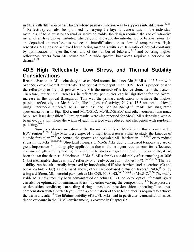
in MLs with diffusion barrier layers whose primary function was to suppress interdiffusion. 33,38-
41 Reflectivity can also be optimized by varying the layer thickness ratio of the individual materials. If MLs must be thermal or radiation stable, the design requires the use of refractive materials such as oxides, carbides, silicides, and alloys, or the introduction of barrier layers that are deposited on interfaces to reduce the interdiffusion due to elevated temperatures. High-resolution MLs can be achieved by selecting materials with a certain ratio of optical constants, by optimization of layer thickness and of the number of bilayers,42-45 and by using higher-reflectance orders from ML structures.46 A wide spectral bandwidth requires a periodic ML design.47,48
4D.5 High Reflectivity, Low Stress, and Thermal Stability Considerations Recent advances in ML technology have enabled normal-incidence Mo-Si MLs at 13.5 nm with over 68% experimental reflectivity. The optical throughput in an EUVL tool is proportional to the reflectivity to the n-th power, where n is the number of reflective elements in the system. Therefore, rather small increases in reflectivity per mirror can be significant for the overall increase in the optical throughput. This was the primary motivation to achieve the highest possible reflectivity on Mo-Si MLs. The highest reflectivity, 70% at 13.5 nm, was achieved using interface-engineered MLs, such as: the Mo/B4C/Si/B4C38 made by magnetron sputtering,shown in Fig. 4D.3), and Mo/C/Si/C, Mo/B4C/Si/B4C and other combinations made by pulsed laser deposition.33 Similar results were also reported for Mo-Si MLs deposited with e-beam evaporation where the width of each interface was reduced and sharpened with ion-beam polishing.26,49
Numerous studies investigated the thermal stability of Mo-Si MLs that operate in the EUV region.38,50-59 The MLs were exposed to high temperatures either to study the kinetics of silicide formation,60-62 to control the growth and optimize ML fabrication,52,54,62,63 or to reduce stress in the MLs.55,56,64,65 Structural changes in Mo-Si MLs due to increased temperature are of great importance for lithography applications due to the stringent requirements for reflectance and wavelength stability and figure errors due to stress changes in the MLs. For example, it has been shown that the period thickness of Mo-Si MLs shrinks considerably after annealing at 300° C, but measurable change in EUV reflectivity already occurs at or above 100°C.55,56,59,66 Thermal stability can be substantially improved by introducing diffusion barriers such as carbon (C) and boron carbide (B4C) as discussed above, other carbide-based diffusion layers,67 SiO2,68 or by using a different ML material pair such as Mo2C/Si, MoSi2/Si,56,57, 54,69 or Mo/SiC.69,70 Thermally stable MLs have recently been demonstrated on actual EUVL collector optics.71,72 ,Multilayers can also be optimized for minimum stress73 by either varying the composition,74-77 base pressure, or deposition condition;78 annealing during deposition; post-deposition annealing;79 or stress compensation with a buffer layer. Often a combination of these techniques is required to achieve the desired results.80 The lifetime stability of EUVL MLs, and in particular, contamination issues due to exposure in the EUVL environment, is covered in Chapter 6A.
(a)
(b)
Figure 4D.3 (a) Cross-sectional transmission electron microscopy (TEM) images of a Mo-Si ML (top left)
and a Mo/B4C/Si/B4C ML with improved interface contrast due to the B4C barrier layers (top right). (b) EUV reflectance curves of the two MLs shown in the TEM images, illustrating the improvement in
reflectance due to the B4C barrier layers. See also Ref. 38. 4D.6 Optical Constants To successfully model and predict the performance of ML coatings for EUVL, precise knowledge of the optical properties of a system’s constituent materials is required. The absorptive and dispersive behavior of each material can be obtained from the real and imaginary part of the wavelength-dependent refractive index, also known as optical constants. In the EUV/x-ray region, where the wavelength of radiation is comparable to the binding energies of the inner electrons in the material, measurements of the refractive index can be particularly challenging due to sensitivity to surface oxides, contamination, and roughness of the material samples under study. Although sophisticated models have been developed to determine the refractive index of materials using first-principles calculations, experimental measurements are always recommended as the best method to accurately determine the refractive index of vapor-deposited thin films. This is especially true for energy regions in the vicinity of electronic absorption edges, where the optical properties can strongly depend on experimental conditions
such as the method and environment of deposition. The optical constants of important EUVL materials for ML coatings such as Si,81 Mo,82,83 Be,84 and Ru85 have been updated in recent years with more accurate experimental results. A comprehensive compilation of the optical constants for all elements in the periodic table, including recently obtained data, are maintained in the Center for X-Ray Optics (CXRO) database86 (and presented in the appendix of this book) and in the IMD software package.87 Other databases for the optical properties of materials in the EUV/x-ray region are maintained by the National Institute of Standards and Technology (NIST)88 and LLNL.89
4D.7 Multilayer Thickness Specifications for Imaging and Condenser EUVL Mirrors Several criteria must be considered when specifying thickness tolerances for reflective, ML-coated optics for EUVL.90 The specifications discussed below apply to the clear aperture of each mirror surface within the EUVL imaging system. As case examples, experimental results from the ML coatings of a four-mirror, 0.1 numerical aperture (NA), full-field system23 (the Engineering Test Stand or ETS) and a two-mirror, 0.3-NA microfield system24 (the microexposure tool or MET) are presented. The applicability of the requirements discussed below on EUVL condenser mirrors is addressed at the end of this section. Throughput: An EUVL scanner consists of an all-reflective optical system with ML coatings on the projection (imaging) elements, on the condenser/illuminator assembly, and on the mask. All of these elements should be tuned to reflect at or near the same wavelength to obtain a substantial output from the system. Any spectral mismatch between the mirrors would translate to throughput reduction. If a goal is set to match the reflectance peak position of all EUVL optics to within ∆λ = ± 0.050 nm, then in a system with six reflections, for example, this level of wavelength-matching would ensure at least 97.4% of the ideal throughput. Meeting this goal requires atomic-level repeatability of the coating process from one deposition run to another. In addition to optic-to-optic wavelength matching, another throughput constraint is the tolerance on wavelength variation across the surface of any individual optic in the system. For maximum throughput, the ML should have its reflectivity peak at the same wavelength for all surface points on any given mirror. If an arbitrary goal is set to stay within 99% of the reflectivity peak for all points on the optic surface, then a Mo-Si ML operating at λ=13.4 nm is allowed to have its wavelength vary to within ∆λ = ± 0.050 nm, which is equivalent to having the wavelength (or the thickness) vary from its prescribed value to within ±0.37% peak-to-valley (P-V) across the surface. Intensity variations: In addition to the throughput constraints discussed above, a reflectivity mismatch—or other causes such as variations in substrate roughness—across any individual mirror surface in the projection system results in intensity variations (apodization) of the reflected wavefront at the system exit pupil. These variations can lead to a narrowing of the NA or a nonuniformity across the pupil. In lithography terms, these effects cause loss of aerial image contrast, and variations in key aberrations and in the critical dimension (CD) of printed images across the field. For example, the tolerance for these effects was determined to be ±0.2% P-V for the wavelength (or thickness) variation across each of the MET and ETS camera optics shown in Figs, 4D.4 and 4D.5.
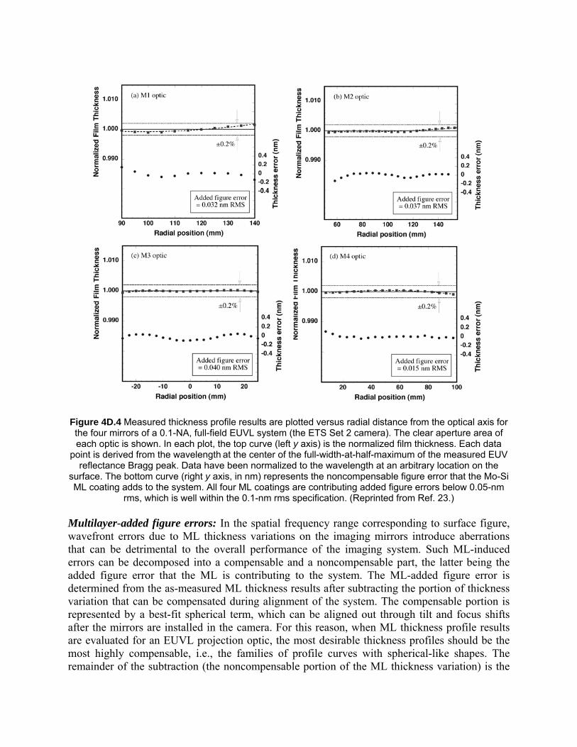
Figure 4D.4 Measured thickness profile results are plotted versus radial distance from the optical axis for the four mirrors of a 0.1-NA, full-field EUVL system (the ETS Set 2 camera). The clear aperture area of each optic is shown. In each plot, the top curve (left y axis) is the normalized film thickness. Each data
point is derived from the wavelength at the center of the full-width-at-half-maximum of the measured EUV reflectance Bragg peak. Data have been normalized to the wavelength at an arbitrary location on the
surface. The bottom curve (right y axis, in nm) represents the noncompensable figure error that the Mo-Si ML coating adds to the system. All four ML coatings are contributing added figure errors below 0.05-nm
rms, which is well within the 0.1-nm rms specification. (Reprinted from Ref. 23.) Multilayer-added figure errors: In the spatial frequency range corresponding to surface figure, wavefront errors due to ML thickness variations on the imaging mirrors introduce aberrations that can be detrimental to the overall performance of the imaging system. Such ML-induced errors can be decomposed into a compensable and a noncompensable part, the latter being the added figure error that the ML is contributing to the system. The ML-added figure error is determined from the as-measured ML thickness results after subtracting the portion of thickness variation that can be compensated during alignment of the system. The compensable portion is represented by a best-fit spherical term, which can be aligned out through tilt and focus shifts after the mirrors are installed in the camera. For this reason, when ML thickness profile results are evaluated for an EUVL projection optic, the most desirable thickness profiles should be the most highly compensable, i.e., the families of profile curves with spherical-like shapes. The remainder of the subtraction (the noncompensable portion of the ML thickness variation) is the
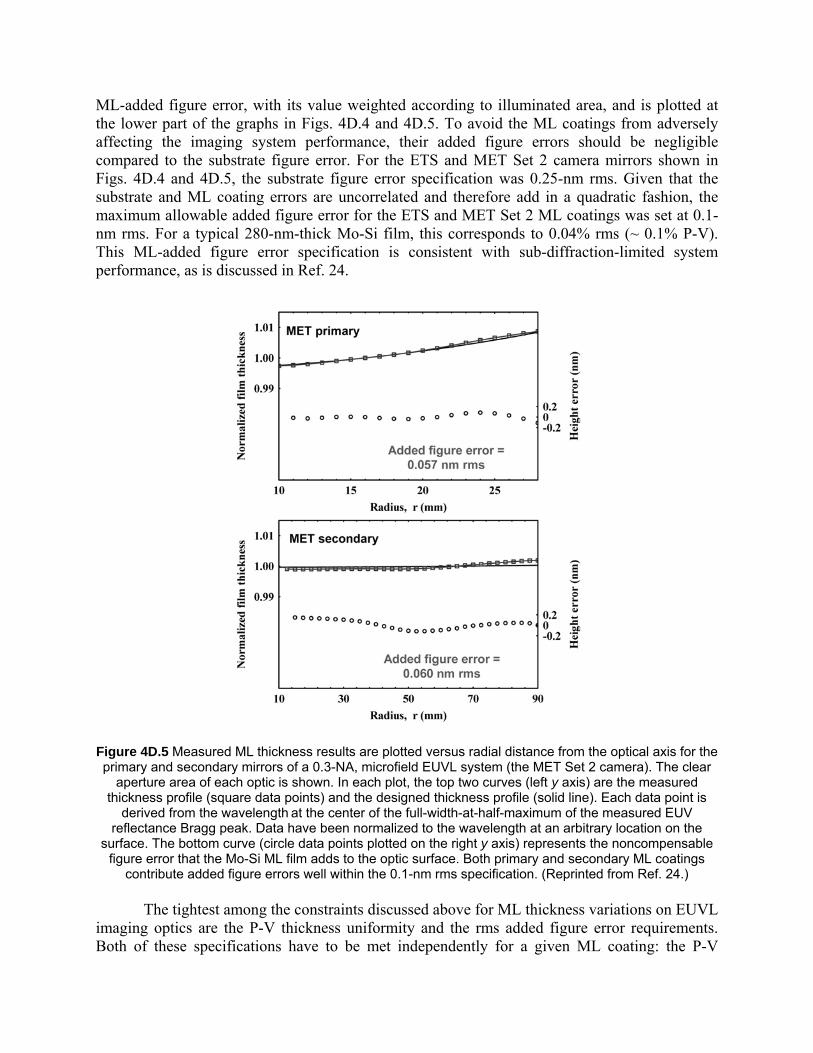
ML-added figure error, with its value weighted according to illuminated area, and is plotted at the lower part of the graphs in Figs. 4D.4 and 4D.5. To avoid the ML coatings from adversely affecting the imaging system performance, their added figure errors should be negligible compared to the substrate figure error. For the ETS and MET Set 2 camera mirrors shown in Figs. 4D.4 and 4D.5, the substrate figure error specification was 0.25-nm rms. Given that the substrate and ML coating errors are uncorrelated and therefore add in a quadratic fashion, the maximum allowable added figure error for the ETS and MET Set 2 ML coatings was set at 0.1-nm rms. For a typical 280-nm-thick Mo-Si film, this corresponds to 0.04% rms (~ 0.1% P-V). This ML-added figure error specification is consistent with sub-diffraction-limited system performance, as is discussed in Ref. 24.
Figure 4D.5 Measured ML thickness results are plotted versus radial distance from the optical axis for the primary and secondary mirrors of a 0.3-NA, microfield EUVL system (the MET Set 2 camera). The clear
aperture area of each optic is shown. In each plot, the top two curves (left y axis) are the measured thickness profile (square data points) and the designed thickness profile (solid line). Each data point is
derived from the wavelength at the center of the full-width-at-half-maximum of the measured EUV reflectance Bragg peak. Data have been normalized to the wavelength at an arbitrary location on the
surface. The bottom curve (circle data points plotted on the right y axis) represents the noncompensable figure error that the Mo-Si ML film adds to the optic surface. Both primary and secondary ML coatings
contribute added figure errors well within the 0.1-nm rms specification. (Reprinted from Ref. 24.) The tightest among the constraints discussed above for ML thickness variations on EUVL imaging optics are the P-V thickness uniformity and the rms added figure error requirements. Both of these specifications have to be met independently for a given ML coating: the P-V

thickness uniformity criterion is applied to the as-measured ML thickness profile, while the added figure error is determined from the noncompensable portion of the as-measured profile (as discussed above). Satisfying the rms added figure error constraint depends to a large degree on the “shape” of the thickness profile, i.e., profile shapes approaching a second-order polynomial are largely compensable during system alignment. During process development of the ETS and MET ML coatings shown in Figs. 4D.4 and 4D.5, it was concluded that the added figure error tolerance requires the tightest control on the coating thickness. For this reason, the thickness profiles presented in Figs. 4D.4 and 4D.5 were optimized primarily for the lowest added figure error rather than P-V uniformity. The next generation of EUVL projection optics is currently being implemented in beta and production tools. Substrate figure requirements have been set at about 0.1-nm rms for these systems. Consequently, ML-added figure errors of less than 0.05-nm rms should be achieved—a factor of 2 more stringent than the ETS and MET camera requirements. Commercial EUVL scanner designs include six-mirror cameras, with the clear aperture extending up to 200 mm from the optical axis, for some of the mirrors. To meet all the additional constraints imposed on EUVL beta and production ML coatings, extremely sophisticated control of the ML film thickness is required. The results presented in Figs. 4D.4 and 4D.5 illustrate the feasibility of meeting such specifications. In the case of EUVL condenser mirrors, the specifications for ML thickness control are more relaxed compared to the projection mirrors because condenser optics are not required to satisfy the stringent figure error (wavefront) requirements discussed above, as explained in Chapter 4C. Slope error specifications are most commonly attached to the figure and mid-spatial frequencies of EUVL condenser optics, driven by displacement considerations of the illumination beam spot. Nevertheless, the throughput requirements discussed above do apply to the ML coatings for condenser elements, and they impose the restrictions on P-V variations of the ML thickness across the optic surface. Acknowledgements The authors gratefully acknowledge the EUV LLC and SEMATECH for their support of the EUVL program at the Lawrence Berkeley, Lawrence Livermore, and Sandia National Laboratories. We also thank Eberhard Spiller for many enlightening discussions. References
1. J. DuMond and J.P. Youtz,“An x-ray method for determining rates of diffusion in the solid state”, J. Appl. Phys. 11, 357–365 (1940).
2. J. Dinklage, ”X-ray diffraction by multilayered thin film structures and their diffusion” J. Appl. Phys. 38, 3781-3785 (1967).
3. E. Spiller, “Low-loss reflection coatings using absorbing materials”, App. Phys. Lett. 20, 365 -367 (1972).
4. T. W. Barbee and D. C. Keith, “Synthetic structures layered on the atomic scale”, in Workshop on Instrumentation for Synchrotron Radiation Research, H. Winick and G. Brown, Eds., Stanford Synchrotron Radiation Laboratory Report 78/04, p. III-36 (1978).
5. J. H. Underwood and T. W. Barbee, “Layered synthetic microstrucutures as Bragg diffractors for X rays and extreme ultraviolet: theory and predicted performance,” Appl. Opt. 20, 3027–3034 (1981).
6. For a comprehensive list of the early efforts on ML coatings for EUV/x-ray lithography, see, for instance, the manuscripts and references in Extreme Ultraviolet Lithography, F. Zernike and D. T. Attwood, Eds., OSA Proc. 23 (1994).
7. M.C. Hettrick and J. H. Underwood, “Stigmatic high throughput monochromator for soft X-rays,” Appl. Opt. 25, 4228–4231 (1986).
8. D. L. Windt and W. K. Waskiewicz, “Soft X-ray reflectometry of multilayer coatings using a laser-plasma source,” Proc. SPIE 1547, 144–158 (1991).
9. E. M. Gullikson, J. H. Underwood, P.C. Batson, and V. Nikitin, “A soft x-ray/EUV reflectometer based on a laser produced plasma source,” J. X-ray Sci. Tech. 3, 283–299 (1992).
10. D. Attwood, “New opportunities at soft x-ray wavelengths,” Physics Today, 24–31 (August 1992).
11. D. A. Tichenor et al, “10x reduction imaging at 13.4 nm,” in Extreme Ultraviolet Lithography, F. Zernike and D. T. Attwood, Eds., OSA Proc. 23, 89-97 (1994).
12. K. M. Skulina, C. S. Alford, R. M. Bionta, et al., “Beryllium-based multilayers for normal incidence EUV reflectance,” in Extreme Ultraviolet Lithography, F. Zernike and D. T. Attwood, Eds., OSA Proc. 23, 52–55 (1994).
13. D. G. Stearns, K. M. Skulina, M. Wall, et al., “Beryllium-based multilayer structures,” in Structure and Properties of Multilayered Thin Films, T. D. Nguyen, B. M. Lairson, B.M. Clemens S.-C. Shin, and K. Sato, Eds., MRS Proc. 382, 329–337 (1995).
14. K. M. Skulina, C. S. Alford, R. M. Bionta, et al., “Molybdenum/beryllium multilayer mirrors for normal incidence in the extreme ultraviolet,” Appl. Opt. 34, 3727–3730 (1995).
15. C. Montcalm, S. Bajt, P. B. Mirkarimi, et al., “Multilayer reflective coatings for extreme ultraviolet lithography,” Proc. SPIE 3331, 42–51 (1998).
16. S. Bajt, R. D. Behymer, P. B. Mirkarimi, et al., “Experimental investigation of beryllium-based multilayer coatings for extreme ultraviolet lithography,” Proc. SPIE 3767, 259–270 (1999).
17. S. Bajt, “Molybdenum-ruthenium/beryllium multilayer coatings,” J. Vac. Sci. Technol. A 18, 557–559 (2000).
18. T. W. Barbee Jr., “Multilayers for x-ray optics,” Opt. Eng. 25, 898–915 (1986). 19. K. L. Choy, “Chemical vapour deposition of coatings,” Prog. in Mater. Sci. 48, 57–170
(2003). 20. V. Vinogradov, “Multilayer x-ray optics,” Quantum Electron. 32, 1113–1121 (2002). 21. T. W. Barbee Jr., S. Mrowka, and M. C. Hettrick, “Molybdenum-silicon multilayer
mirrors for the extreme ultraviolet,” Appl. Opt. 24, 883–886 (1985). 22. C. Montcalm, R. F. Grabner, R. M. Hudyma, et al., “Atomic-precision multilayer coating
of the first set of optics for an extreme-ultraviolet lithography prototype system,” Appl. Opt. 41, 3262–3269 (2002).
23. R. Soufli, E. Spiller, M. A. Schmidt, et al., “Multilayer optics for an extreme ultraviolet lithography tool with 70 nm resolution,” Proc. SPIE 434, 51–59 (2001).
24. R. Soufli, R. M. Hudyma, E. Spiller, et al., “Sub-diffraction-limited multilayer coatings for the 0.3 numerical aperture, micro-exposure tool for extreme ultraviolet lithography,” Appl. Opt. 46, 3736–3746 (2007).
25. E. Louis, E. Zoethout, R. W. E. van de Kruijs, et al., “Multilayer coatings for the EUVL process development tool,” Proc. SPIE 5751, 1170-1177 (2005).
26. E. Louis, A. E. Yakshin, P. C. Görts, et al., “Mo/Si multilayer coating technology for EUVL, coating uniformity and time stability,” Proc. SPIE 4146, 60–63 (2000).
27. E. Spiller, S. L. Baker, P. B. Mirkarimi, et al., “High-performance Mo-Si multilayer coatings for extreme-ultraviolet lithography by ion-beam deposition,” Appl. Opt. 42, 4049–4058 (2003).
28. P. A. Kearney, C. E. Moore, S. I. Tan, S. P. Vernon, and R. A. Levesque, “Mask blanks for extreme ultraviolet lithography: ion beam sputter deposition of low defect density Mo/Si multilayers,” J. Vac. Sci., Technol. B 15, 2452–2454 (1997).
29. T. Chassé, H. Neumann, B. Ocker, et al., “Mo/Si multilayers for EUV lithography by ion beam sputter deposition,” Vacuum 71, 407–415 (2003).
30. T. Chassé, H. Neumann, and B. Rauschenbach, “Ion beam assisted deposition of multi-layer x-ray mirrors for the extreme ultraviolet lithography,” NIM B 206, 377–381 (2003).
31. D.-E. Kim, S.-M. Lee, I.-J. Jeon, and M. Yanagihara, “Characterization of a multilayer soft x-ray reflector fabricated by pulsed laser deposition,” Appl. Surf. Sci. 127-129, 531–535 (1998).
32. S. Braun, R. Dietsch, M. Haidl, et al., “Mo/Si multilayers for EUV application prepared by pulsed laser deposition (PLD),” Microelectron. Eng. 57-58, 9–15 (2001).
33. S. Braun, H. Mai, M. Moss, R. Scholz, and A. Leson, “Mo/Si multilayers with different barrier layers for applications at extreme ultraviolet mirrors,” Jap. J. Appl. Phy. 41, 4074–4081 (2002).
34. E. Spiller, Soft X-Ray Optics, SPIE Press, Bellingham, WA (1994). 35. J. I. Larruquert, “Sub-quarterwave multilayers with enhanced reflectance at 13.4 and 11.3
nm,” Opt. Comm. 206, 259–273 (2002). 36. J. I. Larruquert, “Reflectance enhancement in the extreme ultraviolet and soft x-rays by
means of multilayers with more than two materials,” J. Opt. Soc. Am. A 19, 391–397 (2002).
37. M. Singh, and J. M. Braat, “Design of multilayer extreme ultraviolet mirrors for enhanced reflectivity,” Appl. Opt. 39, 2189–2197 (2000).
38. S. Bajt, J. B. Alameda, T. W. Barbee Jr., et al., “Improved reflectance and stability of Mo-Si multilayers,” Opt. Eng. 41, 1797-1804 (2002).
39. S. Yulin, N. Benoit, T. Faigl, and N. Kaiser, “Interface-engineered EUV multilayer mirrors,” Microelect. Eng. 83, 692–694 (2006).
40. H. Maury, P. Jonnard, J.-M. André, et al., “Non-destructive X-ray study of the interphases in Mo/Si and Mo/B4C/Si/B4C multilayers,” Thin Solid Films 514, 278–286 (2006).
41. L. G. A. M. Alink, R. W. E. van de Kruijs, E. Louis, F. Bijkerk, and J. Verhoeven, “Improved temperature stability of Mo/Si multilayers by carbide based diffusion barriers through implantation of low energy CHx
+ ions,” Thin Solid Films 510, 26–31 (2006). 42. V. Arkadiev, A. Baranov, A. Erko, et al., “Carbon/carbon multilayers for synchrotron
radiation,” Proc. SPIE 3773, 122–127 (1999). 43. C. Morawe, J.-C. Peffen, E. Ziegler, and A. K. Freund, “High resolution multilayer x-ray
optics,” Proc. SPIE 4145, 61–71 (2001). 44. R. Dietsch, T. Holz, H. Mai, et al., “X-ray optical properties of C/C multilayers prepared
by pulsed laser deposition (PLD),” Proc. MRS 382, 345–350 (1995).
45. Y. C. Lim, T. Westerwalbesloh, A. Aschentrup, et al., “Fabrication and characterization of EUV multilayer mirrors optimized for small spectra reflection bandwidth,” Appl. Phys. A 72, 121–124 (2001).
46. S. Yulin, T. Kuhlmann, T. Feigi, and N. Kaiser, “Spectral reflectance tuning of EUV mirrors for metrology applications,” Proc. SPIE 5037, 286–293 (2003).
47. L. Beigman, A. P. Pirozhkov, and E. N. Ragozin, “Reflection of a few cycle x-ray pulses by aperiodic multilayer structures” J. Opt. A, Pure Appl. Opt. 4, 433-439 (2002).
48. A. Wonisch, Th. Westerwalbesloh, W. Hachmann, et al., “Aperiodic nanometer multilayer systems as optical key components for attosecond electron spectroscopy”, Thin Solid Films 464-465, 473–477 (2004).
49. A.E. Yakshin, R.W.E. van de Kruijs, I. Nedelcu, et al., “Enhanced reflectance of interface engineered Mo/Si multilayers produced by thermal particle deposition,” Proc. SPIE 6517, 65170I (2007).
50. H. Takenaka and T. Lawamura, “Thermal stability of Mo/C/Si/C multilayer soft x-ray mirrors,” J. of Elec. Spec. and Rel. Phenom. 80, 381384 (1996).
51. Z. Jiang, X. Jiang, W. Liu, and Z. Wu, “Thermal stability of multilayer films Pt/Si, W/Si, Mo/Si, and W/Si,” J. Appl. Phys. 65, 196–200 (1989).
52. Kloidt, K. Nolting, U. Kleineberg, et al., “Enhancement of the reflectivity of Mo/Si multilayer mirrors by thermal treatment,” Appl. Phys. 58, 2601–2603 (1991).
53. R. S. Rosen, D. G. Stearns, M. A. Villiardos, et al., “Silicide layer growth rates in Mo/Si multilayers,” Appl. Opt. 32, 6975–6980 (1993).
54. V. V. Kondratenko, Yu. P. Pershin, O. V. Poltseva, et al., ”Thermal stability of soft x-ray Mo-Si and MoSi2-Si multilayer mirros,” Appl. Opt. 32, 18111816 (1993).
55. D. L. Windt, “Stress, microstructure, and stability of Mo/Si, W/Si, and Mo/C multilayer films,” J. Vac. Sci. Technol. A 18, 980–991 (2000).
56. T. Feigl, H. Lauth, S. Yulin, and N. Kaiser, “Heat resistance of EUV multilayer mirrors for long-time applications,” Microelectr. Eng. 57-58, 3–8 (2001).
57. T. Feigl, S. Yulin, T. Kuhlmann, and N. Kaiser, “Damage resistant and low stress EUV multilayer mirrors,” Jpn. J. Appl. Phys. 41, 4082 4085 (2002).
58. T. Böttger, D. C. Meyer, P. Paufler, et al., “Thermal stability of Mo/Si multilayers with boron carbide interlayers,” Thin Solid Films 444, 165–173 (2003).
59. H. Takenaka, H. Io, T. Haga, and T. Kawamura, “Design and fabrication of highly heat-resistant Mo/Si multilayer soft x-ray mirrors with interleaved barrier layers,” J. Synchrotron Rad. 5, 708–710 (1998).
60. Z. Jiang, X. Jiang, W. Liu, and Z. Wu, “Thermal stability of multilayer films Pt/Si, W/Si, Mo/Si, and W/Si,” J. Appl. Phys. 65, 196–200 (1989).
61. Y. Ijdiyaou, M. Azizan, E. L. Ameziane, M. Brunel, and T. A. N. Tan, “On the formation of molybdenum silicides in Mo-Si multilayers: the effect of Mo thickness and annealing temperature,” Appl. Surf. Scien. 55, 165–171 (1992).
62. H.-J. Voorma, E. Louis, N. B. Koster, and F. Bijkerk, “Temperature induced diffusion in Mo/Si multilayer mirrors,” J. Appl. Phys. 83, 4700–4708 (1998).
63. J. M. Liang and L. J. Chen, “Interfacial reactions and thermal stability of ultrahigh vacuum deposited multilayered Mo/Si structures,” J. Appl. Phys. 79, 4072–4077 (1996).
64. R. R. Kola, D. L. Windt, W. K. Waskiewicz, et al., “Stress relaxation in Mo/Si multilayer structures,” Appl. Phys. Lett. 60, 3120–3122 (1992).
65. T. Leisegang, D. C. Meyer, A. A. Levin, S. Braun, and P. Paufler, “On the interplay of internal/external stress and thermal stability of Mo/Si multilayers,” Appl. Phys. A 77, 965–972 (2003).
66. H. Azuma, A. Takeichi, I. Konomi, Y. Watanabe, and S. Noda, “Thermally induces structural modification of nanometer-order Mo/Si multilayers by the spectral reflectance of laser-plasma soft X-rays,” Jpn. J. Appl. Phys. 43, 2078–2082 (1993).
67. L.G. A. M. Alink, R. W. E. van de Kruijs, E. Louis, F. Bijkerk, and J. Verhoeven, “Improved temperature stability of Mo/Si multilayers by carbide based diffusion barriers through implantation of low energy CHx ions,” Thin Solid Films 510, 26–31 (2006).
68. M. Ishino, O. Yoda, H. Takenaka, K. Sano, and M. Koike, “Heat stability of Mo/Si multilayers inserted with compound layers,” Surf. Coat. Technol. 169-170, 628–631 (2003).
69. H. Takenaka, T. Kawamura, Y. Ishii, T. Haga, and H. Kinoshita, “Evaluation of Mo-based multilayer EUV mirrors,”in Extreme Ultraviolet Lithography, F. Zernike and D. T. Attwood, Eds., OSA Proc. 23, 26–32 (1994).
70. S. Bajt and D. G. Stearns, “High-temperature stability multilayers for extreme ultraviolet condenser optics,” Appl. Opt. 44, 7735–7743 (2005).
71. S. Yulin, N. Benoit, T. Feigl, and N. Kaiser, “High-temperature multilayers,” Proc. SPIE 5751, 1155–1161 (2005).
72. T. Feig, S. Yulin, N. Benoit, et al., “High-temperature LPP collector mirror,” Proc. SPIE 6151, 61514A (2006).
73. P. B. Mirkarimi, “Stress, reflectance, and temporal stability of sputter-deposited Mo/Si and Mo/Be multilayer films for extreme ultraviolet lithography,” Opt. Eng. 38, 1246–1259 (1999).
74. T. D. Nguyen, X. Lu, and J. H. Underwood, “Stress characterization in periodic multilayer structures for x-ray optics,” in Physics of X-ray Multilayer Structures, Vol. 6, pp. 103–105, Optical Society of America, Washington, D.C. (1994).
75. T. D. Nguyen, C. Khan-Malek, and J. H. Underwood, “Achievement of low stress in Mo/Si multilayer mirrors,” in OSA Proc. on Extreme Ultraviolet Lithography, F. Zernike and D. T. Atwood, Eds., Vol. 23, pp. 56–59, Optical Society of America, Washington, D.C. (1994).
76. D. L. Windt, W. L. Brown, and C. A. Volkert, “Variation in stress with background pressure in sputtered Mo/Si multilayer films,” J. Appl. Phys. 78, 2423–2430 (1995).
77. M. C. K. Tinone, T. Haga, and H. Kinoshita, “Multilayer sputter deposition stress control,” J. Electron. Spectrosc. Relat. Phenom. 80, 461–464 (1996).
78. S. P. Vernon, D. G. Stearns, and R. S. Rosen, “Ion-assisted sputter deposition of molybdenum-silicon multilayers,” Appl. Opt. 32, 6969–6974 (1993).
79. C. Montcalm, “Reduction of residual stress in extreme ultraviolet Mo/Si multilayer mirrors with postdeposition thermal treatments,” Opt. Eng. 40, 469–477 (2001).
80. M. Moss, T. Böttger, S. Braun, T. Foltyn, and A. Leson, “Stress compensation of a Mo/Si/C highly reflective multilayer by means of an optimized buffer layer and heat treatment,” Thin Solid Films 468, 322–331 (2004).
81. R. Soufli and E. M. Gullikson, “Reflectance measurements on clean surfaces for the determination of optical constants of silicon in the extreme ultraviolet-soft-x-ray region,” Appl. Opt. 36, 5499–5507 (1997).
82. R. Soufli and E. M. Gullikson, “Absolute photoabsorption measurements of molybdenum in the range 60 to 930 eV for optical constant determination,” Appl. Opt. 37, 1713–19 (1998).
83. C. Tarrio, R. N. Watts, T. B. Lucatorto, J. M. Slaughter, and C. M. Falco, “Optical constants of in situ-deposited films of important extreme-ultraviolet multilayer mirror materials,” Appl. Opt. 37, 4100–4104 (1998).
84. R. Soufli, S. Bajt, and E. M. Gullikson, “Optical constants of beryllium from photoabsorption measurements for x-ray optics applications,” Proc. SPIE 3767, 251–256 (1999).
85. U. Schlegel, “Determination of the optical constants of Ruthenium in the EUV and soft x-ray region using synchrotron radiation,” Diploma thesis, Technische Fachhochschule Berlin, May 2000.
86. B. L. Henke, E. M. Gullikson, and J. C. Davis, “X-ray interactions: photoabsorption, scattering, transmission, and reflection at E = 50–30,000 eV, Z = 1–92,” At. Data Nucl. Data Tables 54, 181–342 (1993). The updated version of these data is available at http://henke.lbl.gov/optical_constants/asf.html.
87. D. L. Windt, “IMD-software for modeling the optical properties of multilayer films,” Computers in Physics 12, 360–370 (1998). IMD software is available at http://www.rxollc.com/idl.
88. X-Ray and Gamma-Ray Data, http://physics.nist.gov/PhysRefData/contents-xray.html. 89. Elastic Photon-Atom Scattering, http://physci.llnl.gov/Research/scattering/ 90. D. W. Sweeney, R. M. Hudyma, H. N. Chapman, and D. Shafer, “EUV optical design for
a 100 nm CD imaging system,” Proc. SPIE 3331, 2–10 (1998).
This work performed under the auspices of the U.S. Department of Energy by Lawrence Livermore National Laboratory under Contract DE-AC52-07NA27344.
Regina Soufli received her Ph.D. in Electrical Engineering from the University of California, Berkeley, in 1997, and was staff scientist at the Harvard-Smithsonian Center for Astrophysics in 1997-99, studying the optical properties of iridium-coated mirrors for NASA’s Chandra X-ray Observatory. She joined LLNL in 1999 and has been the principal investigator on EUV/x-ray optics programs for semiconductor lithography, solar physics, synchrotron and free-electron lasers, and high-energy physics. Her interests are in EUV/x-ray interactions with matter, surface science, thin films, roughness and
scattering. She has received several LLNL awards and two “R&D 100” awards while at LLNL. Saša Bajt received her PhD in Physics at the University of Heidelberg in Germany. She worked for The University of Chicago at the National Synchrotron Light Source (NSLS) developing x-ray fluorescence microprobe and microx-ray spectroscopy. She joined Lawrence Livermore National Laboratory in 1996 where she was a principal investigator of a multilayer development team. As of 2008, she leads a Novel X-ray Optics group at DESY (Hamburg, Germany). She was a recipient of the Hawley medal in 1999, given by The Mineralogical Association of Canada, for the innovation
and application of microbeam XAFS to mineralogical research, and she has also received several LLNL awards. She holds several US and international patents on novel multilayer structures. Her protective capping layer design to extend the lifetime of the EUV multilayers was accepted as a benchmark by the semiconductor industry. Her research interests include multilayer optics for EUV and x-ray regions, optics damage and lifetime, physics of surfaces and interfaces, and x-ray microscopy and spectroscopy. She is currently developing optics for short pulsed Free Electron Lasers (FELs) and is studying the damage of the coatings exposed to extreme conditions.
Russell M. Hudyma received his BS and MS degrees in Optics from the University of Rochester. He specializes in the field of optical design, analysis, and simulation for a wide range of applications, including remote sensing, surveillance and defense systems, microlithography and semiconductor process. Over 100 of his designs have been built and implemented into commercial systems. He holds 83 U.S. and international patents, most of which are related to optical systems for semiconductor applications. He is the co-founder and managing partner of Hyperion Development, LLC.
John S. Taylor leads the Precision Systems and Manufacturing Groups at LLNL and is the Chief Engineer for fabricating targets for the National Ignition Facility. He previously led LLNL’s X-Ray Optics Group and EUV Lithography Program, which designed and constructed the first wide-field diffraction-limited EUVL imaging cameras. His experience includes optical manufacturing, diamond turning, and metrology. He received his PhD in Mechanical Engineering from Purdue University in 1984. In his work at LLNL, he was awarded five US patents and three R&D 100 Awards. He is a
member of the Optical Society of America, the American Society of Mechanical Engineers, a charter member of the American Society for Precision Engineering, and a Fellow of SPIE.


![EUVL Symposium HVM FINAL 2004[1]](https://img.pdfslide.us/doc/110x75/55c513d9bb61ebc37e8b4574/euvl-symposium-hvm-final-20041.jpg)