Embed Size (px)
Citation preview
TM
TEA-CIM-10705990 0
2014 International Symposium on EUVL
EUVL Convergence with Multi-Patterning Technologies
Akihisa Sekiguchi, Ph.D
Corporate Vice President and Deputy General Manager
Tokyo Electron Limited

TM
TEA-CIM-10705990 1
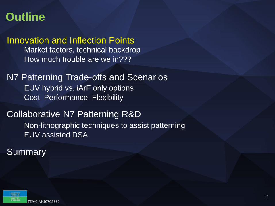
Innovation and Inflection Points
N7 Patterning Trade-offs and Scenarios
Collaborative N7 Patterning R&D
Summary
Market factors, technical backdrop How much trouble are we in???
EUV hybrid vs. iArF only options Cost, Performance, Flexibility
Non-lithographic techniques to assist patterning EUV assisted DSA
Outline
TM
TEA-CIM-10705990 2
Innovation and Inflection Points
N7 Patterning Trade-offs and Scenarios
Collaborative N7 Patterning R&D
Summary
Market factors, technical backdrop How much trouble are we in???
EUV hybrid vs. iArF only options Cost, Performance, Flexibility
Non-lithographic techniques to assist patterning EUV assisted DSA
Outline
TM
TEA-CIM-10705990 3
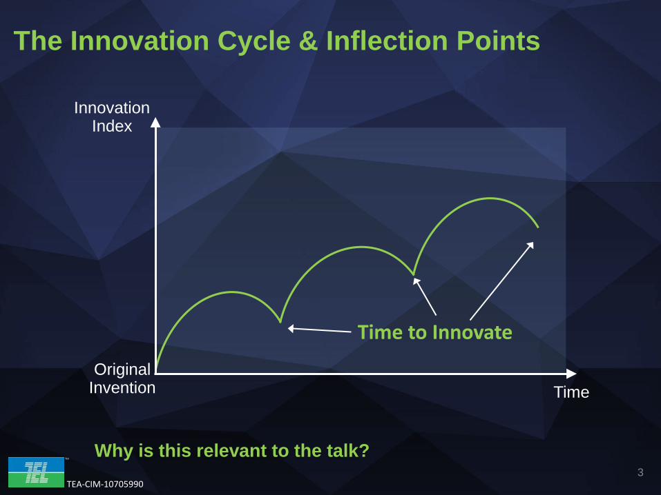
The Innovation Cycle & Inflection Points
Innovation Index
Original Invention Time
Time to Innovate
Why is this relevant to the talk?
TM
TEA-CIM-10705990 4
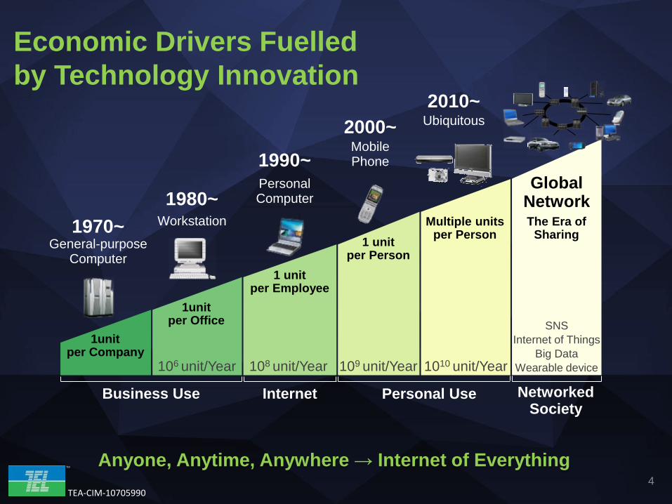
Business Use Personal Use
2010~
Global Network
1970~ 1980~
1990~
2000~
General-purpose Computer
Workstation
Personal Computer
Mobile Phone
Ubiquitous
106 unit/Year 108 unit/Year 1010 unit/Year
SNS Internet of Things
Big Data Wearable device 109 unit/Year
Anyone, Anytime, Anywhere → Internet of Everything
1unit per Company
1unit per Office
1 unit per Employee
1 unit per Person
Multiple units per Person
The Era of Sharing
Networked Society
Internet
Economic Drivers Fuelled by Technology Innovation
TM
TEA-CIM-10705990 5
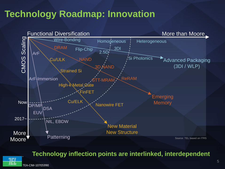
More Moore
Functional Diversification
CM
OS
Sca
ling
New Material New Structure
Advanced Packaging (3DI / WLP)
Heterogeneous 3DI
Strained Si
High-k Metal Gate
Cu/ULK
FinFET
Patterning
ArF
ArF-Immersion
EUV
More than Moore
DP/MP
NIL, EBDW
Flip-Chip 2.5D
Wire-Bonding
Si Photonics
Homogeneous DRAM
NAND
STT-MRAM
3D NAND
ReRAM
Emerging Memory
DSA Now
2017~
Technology inflection points are interlinked, interdependent
Source: TEL based on ITRS
Nanowire FET Cu/ELK
Technology Roadmap: Innovation
TM
TEA-CIM-10705990 6
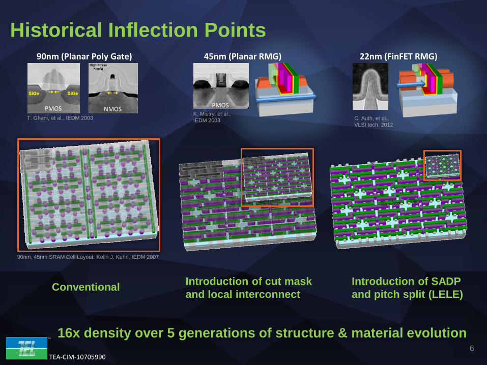
Historical Inflection Points 90nm (Planar Poly Gate) 45nm (Planar RMG) 22nm (FinFET RMG)
PMOS NMOS PMOS
T. Ghani, et al., IEDM 2003 K. Mistry, et al., IEDM 2003 C. Auth, et al.,
VLSI tech. 2012
90nm, 45nm SRAM Cell Layout: Kelin J. Kuhn, IEDM 2007
Introduction of cut mask and local interconnect Conventional Introduction of SADP
and pitch split (LELE)
16x density over 5 generations of structure & material evolution
TM
TEA-CIM-10705990 7
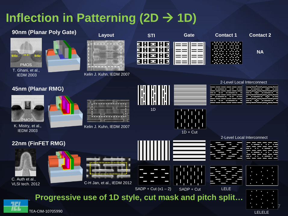
Inflection in Patterning (2D 1D) 90nm (Planar Poly Gate)
PMOS T. Ghani, et al.,
IEDM 2003
45nm (Planar RMG)
K. Mistry, et al., IEDM 2003
PMOS
22nm (FinFET RMG)
C. Auth et al., VLSI tech. 2012
Kelin J. Kuhn, IEDM 2007
Kelin J. Kuhn, IEDM 2007
STI Gate Contact 1 Contact 2
1D
1D + Cut
SADP + Cut SADP + Cut (x1 – 2)
2-Level Local Interconnect
2-Level Local Interconnect
LELE
LELELE
Layout
NA
Progressive use of 1D style, cut mask and pitch split…
C-H Jan, et al., IEDM 2012
TM
TEA-CIM-10705990 8
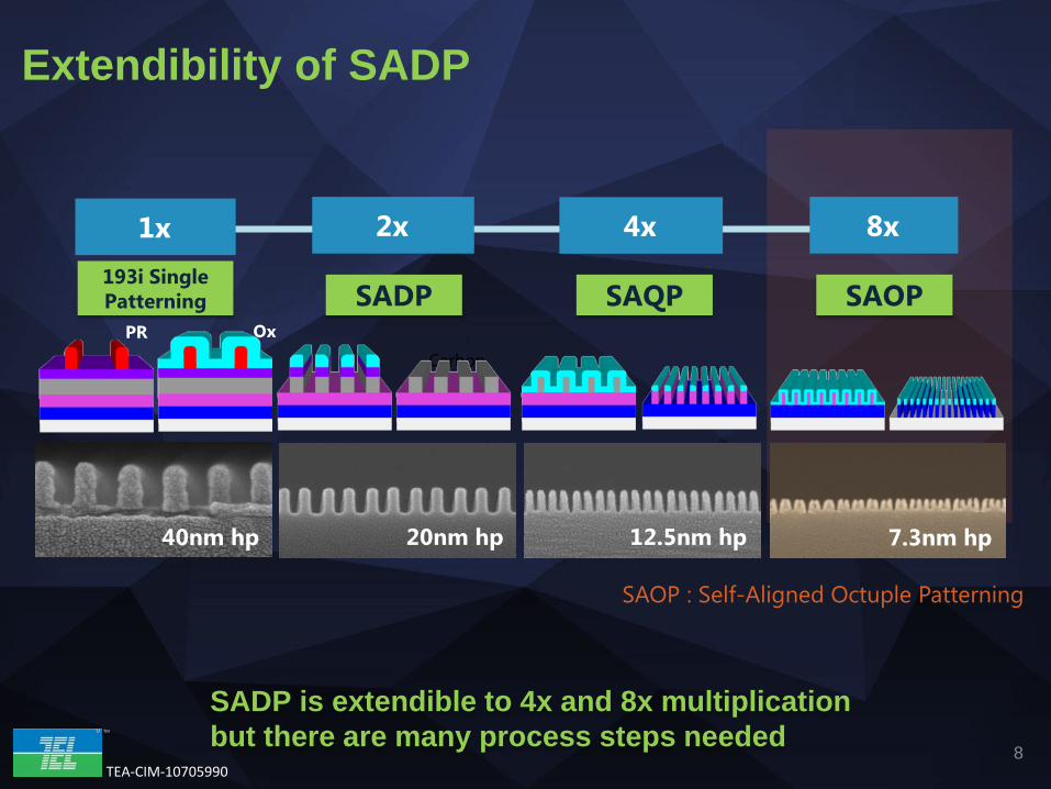
Extendibility of SADP
SAQP
40nm hp 20nm hp 12.5nm hp
SAOP SADP
1x 2x 4x 8x
PR Carbon
193i Single Patterning
7.3 nm hp
SAOP : Self-Aligned Octuple Patterning
Ox
SADP is extendible to 4x and 8x multiplication but there are many process steps needed
7.3nm hp
TM
TEA-CIM-10705990
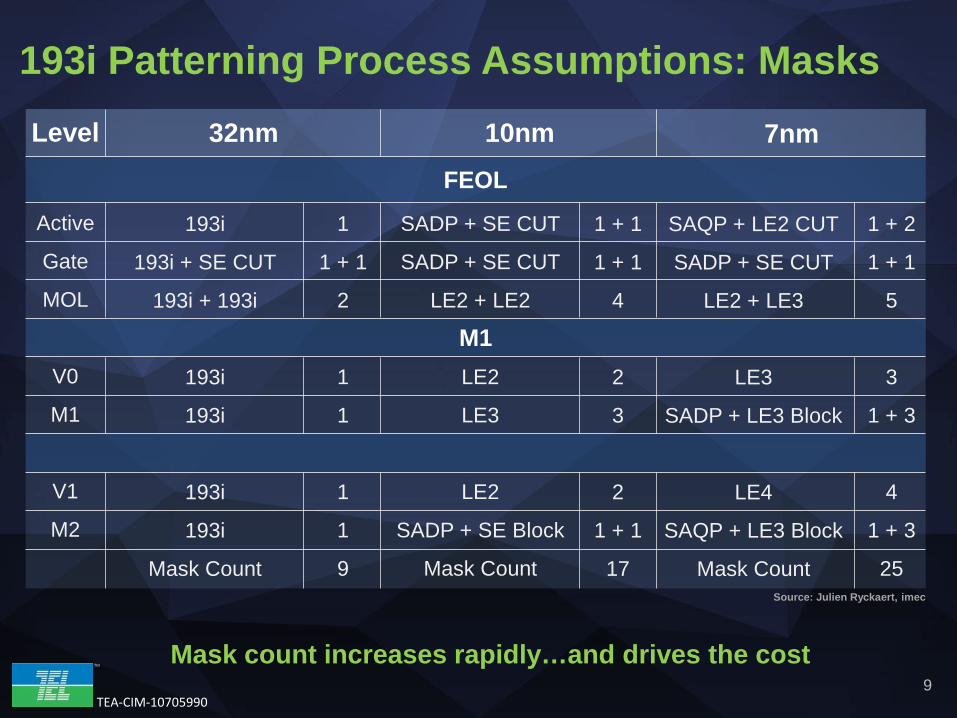
Mask count increases rapidly…and drives the cost
193i Patterning Process Assumptions: Masks
Level
Active
Gate
MOL
V0
M1
V1
M2
193i
193i + SE CUT
193i + 193i
193i
193i
193i
193i
Mask Count
FEOL
M1
1
1 + 1
2
1
1
1
1
9
SADP + SE CUT
SADP + SE CUT
LE2 + LE2
LE2
LE3
LE2
SADP + SE Block
Mask Count
SAQP + LE2 CUT
SADP + SE CUT
LE2 + LE3
LE3
SADP + LE3 Block
LE4
SAQP + LE3 Block
Mask Count
1 + 2
1 + 1
5
3
1 + 3
4
1 + 3
25
32nm 10nm 7nm
1 + 1
1 + 1
4
2
3
2
1 + 1
17
9
Source: Julien Ryckaert, imec
TM
TEA-CIM-10705990
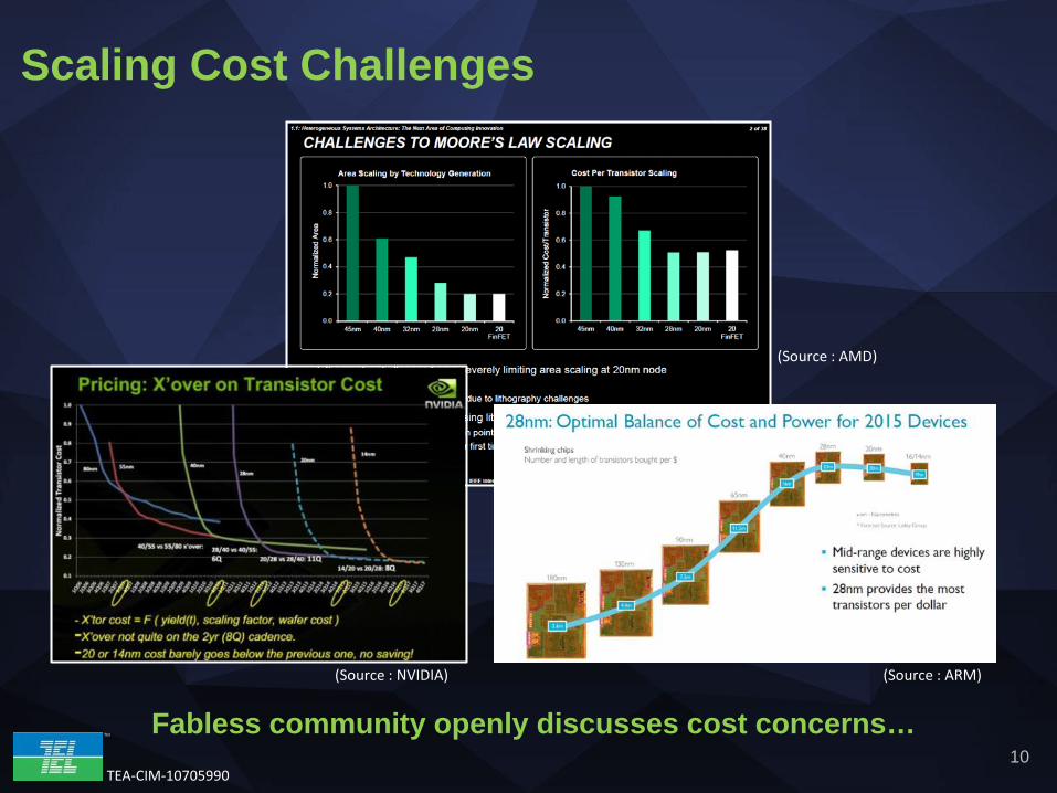
Scaling Cost Challenges
Fabless community openly discusses cost concerns…
(Source : ARM) (Source : NVIDIA)
(Source : AMD)
10
TM
TEA-CIM-10705990 11
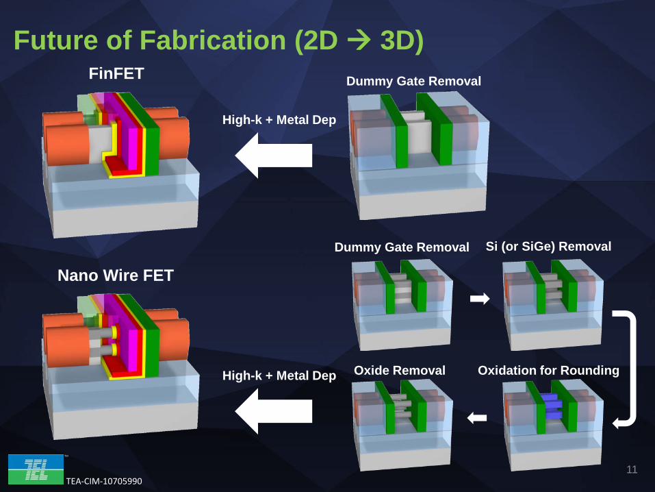
Future of Fabrication (2D 3D) FinFET Dummy Gate Removal
High-k + Metal Dep
Nano Wire FET
Dummy Gate Removal Si (or SiGe) Removal
High-k + Metal Dep Oxidation for Rounding Oxide Removal

TM
TEA-CIM-10705990 12
TM
TEA-CIM-10705990 13
Innovation and Inflection Points
N7 Patterning Trade-offs and Scenarios
Collaborative N7 Patterning R&D
Summary
Market factors, technical backdrop How much trouble are we in???
EUV hybrid vs. iArF only options Cost, Performance, Flexibility
Non-lithographic techniques to assist patterning EUV assisted DSA
Outline
TM
TEA-CIM-10705990 14
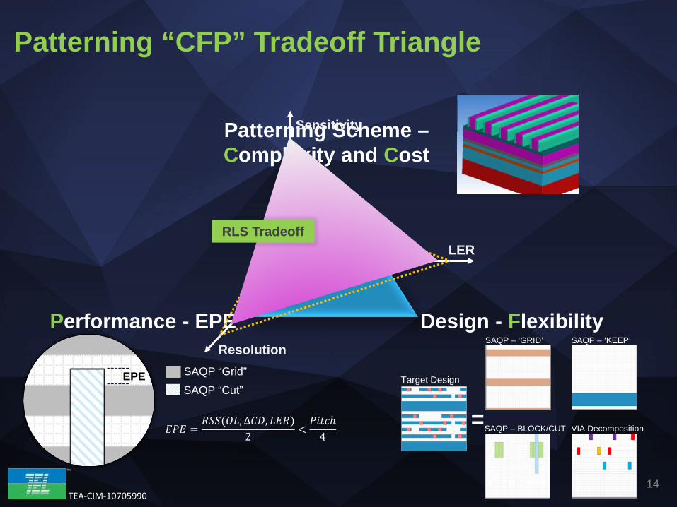
Patterning “CFP” Tradeoff Triangle
Patterning Scheme – Complexity and Cost
Design - Flexibility Performance - EPE
EPE
𝐸𝐸𝐸𝐸𝐸𝐸 =𝑅𝑅𝑅𝑅𝑅𝑅(𝑂𝑂𝑂𝑂,∆𝐶𝐶𝐶𝐶, 𝑂𝑂𝐸𝐸𝑅𝑅)
2<𝐸𝐸𝑃𝑃𝑃𝑃𝑃𝑃𝑃
4
SAQP “Grid”
SAQP “Cut”
=
Target Design
SAQP – ‘GRID’ SAQP – ‘KEEP’
SAQP – BLOCK/CUT VIA Decomposition
RLS Tradeoff LER
Sensitivity
Resolution
TM
TEA-CIM-10705990 15
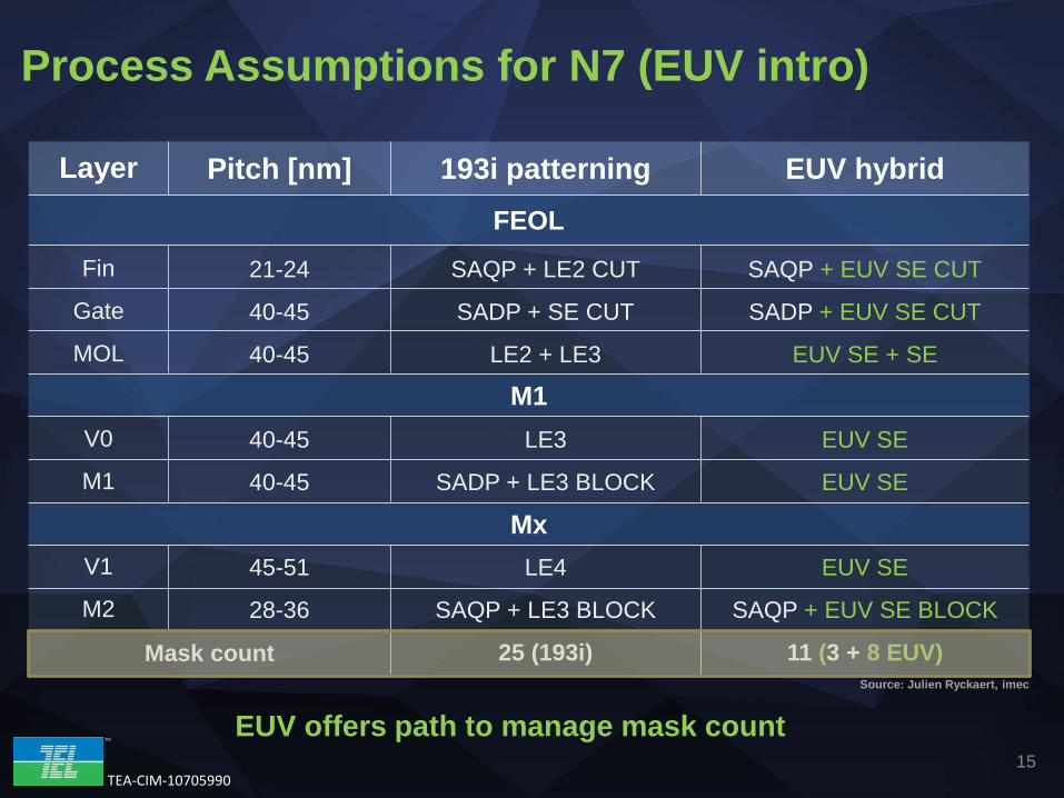
Process Assumptions for N7 (EUV intro)
Layer
Fin
Gate
MOL
V0
M1
V1
M2
Pitch [nm]
21-24
40-45
40-45
40-45
40-45
45-51
28-36
193i patterning
SAQP + LE2 CUT
SADP + SE CUT
LE2 + LE3
LE3
SADP + LE3 BLOCK
LE4
SAQP + LE3 BLOCK
25 (193i)
EUV hybrid
SAQP + EUV SE CUT
SADP + EUV SE CUT
EUV SE + SE
EUV SE
EUV SE
EUV SE
SAQP + EUV SE BLOCK
11 (3 + 8 EUV)
FEOL
M1
Mx
Mask count Source: Julien Ryckaert, imec
EUV offers path to manage mask count
TM
TEA-CIM-10705990 16
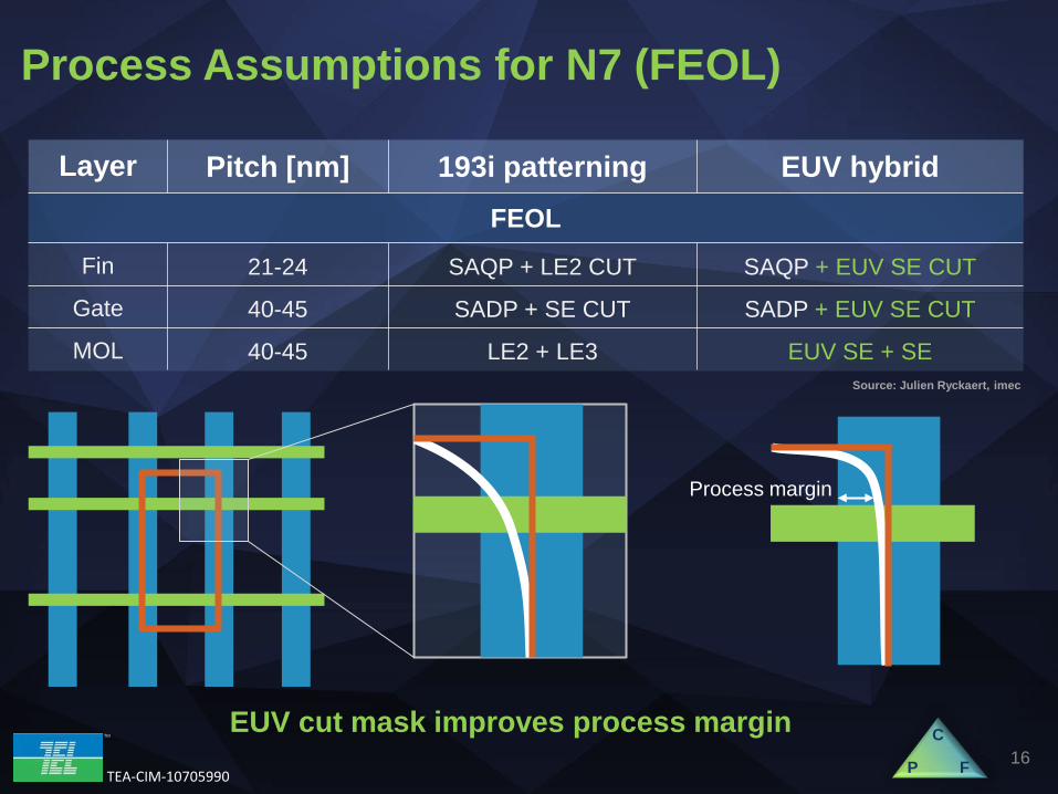
Process Assumptions for N7 (FEOL)
Layer
Fin
Gate
MOL
Pitch [nm]
21-24
40-45
40-45
193i patterning
SAQP + LE2 CUT
SADP + SE CUT
LE2 + LE3
EUV hybrid
SAQP + EUV SE CUT
SADP + EUV SE CUT
EUV SE + SE
FEOL
Process margin
EUV cut mask improves process margin
P
C
F
Source: Julien Ryckaert, imec
TM
TEA-CIM-10705990 17
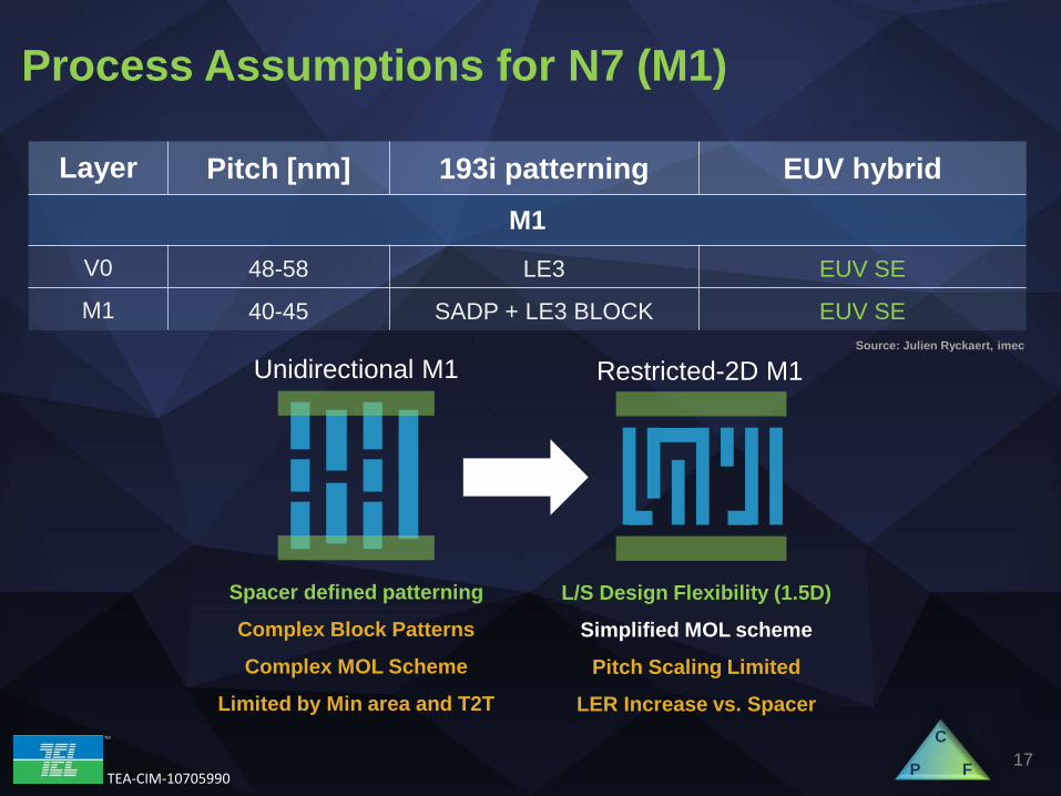
Process Assumptions for N7 (M1)
Layer
V0
M1
Pitch [nm]
48-58
40-45
193i patterning
LE3
SADP + LE3 BLOCK
EUV hybrid
EUV SE
EUV SE
M1
Unidirectional M1 Restricted-2D M1
Spacer defined patterning
Complex Block Patterns
Complex MOL Scheme
Limited by Min area and T2T
L/S Design Flexibility (1.5D)
Simplified MOL scheme
Pitch Scaling Limited
LER Increase vs. Spacer
P
C
F
Source: Julien Ryckaert, imec
TM
TEA-CIM-10705990 18
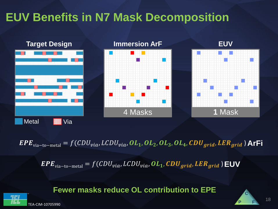
EUV Benefits in N7 Mask Decomposition
𝑬𝑬𝑬𝑬𝑬𝑬via−to−metal = 𝑓𝑓(𝐶𝐶𝐶𝐶𝐶𝐶𝑣𝑣𝑣𝑣𝑣𝑣, 𝑂𝑂𝐶𝐶𝐶𝐶𝐶𝐶𝑣𝑣𝑣𝑣𝑣𝑣,𝑶𝑶𝑶𝑶𝟏𝟏,𝑶𝑶𝑶𝑶𝟐𝟐,𝑶𝑶𝑶𝑶𝟑𝟑,𝑶𝑶𝑶𝑶𝟒𝟒,𝑪𝑪𝑪𝑪𝑪𝑪𝒈𝒈𝒈𝒈𝒈𝒈𝒈𝒈,𝑶𝑶𝑬𝑬𝑳𝑳𝒈𝒈𝒈𝒈𝒈𝒈𝒈𝒈 )
Immersion ArF
4 Masks
EUV
1 Mask
𝑬𝑬𝑬𝑬𝑬𝑬via−to−metal = 𝑓𝑓(𝐶𝐶𝐶𝐶𝐶𝐶𝑣𝑣𝑣𝑣𝑣𝑣, 𝑂𝑂𝐶𝐶𝐶𝐶𝐶𝐶𝑣𝑣𝑣𝑣𝑣𝑣,𝑶𝑶𝑶𝑶𝟏𝟏,𝑪𝑪𝑪𝑪𝑪𝑪𝒈𝒈𝒈𝒈𝒈𝒈𝒈𝒈,𝑶𝑶𝑬𝑬𝑳𝑳𝒈𝒈𝒈𝒈𝒈𝒈𝒈𝒈 )
ArFi
EUV
Fewer masks reduce OL contribution to EPE
Target Design
Metal Via
P
C
F
TM
TEA-CIM-10705990 19
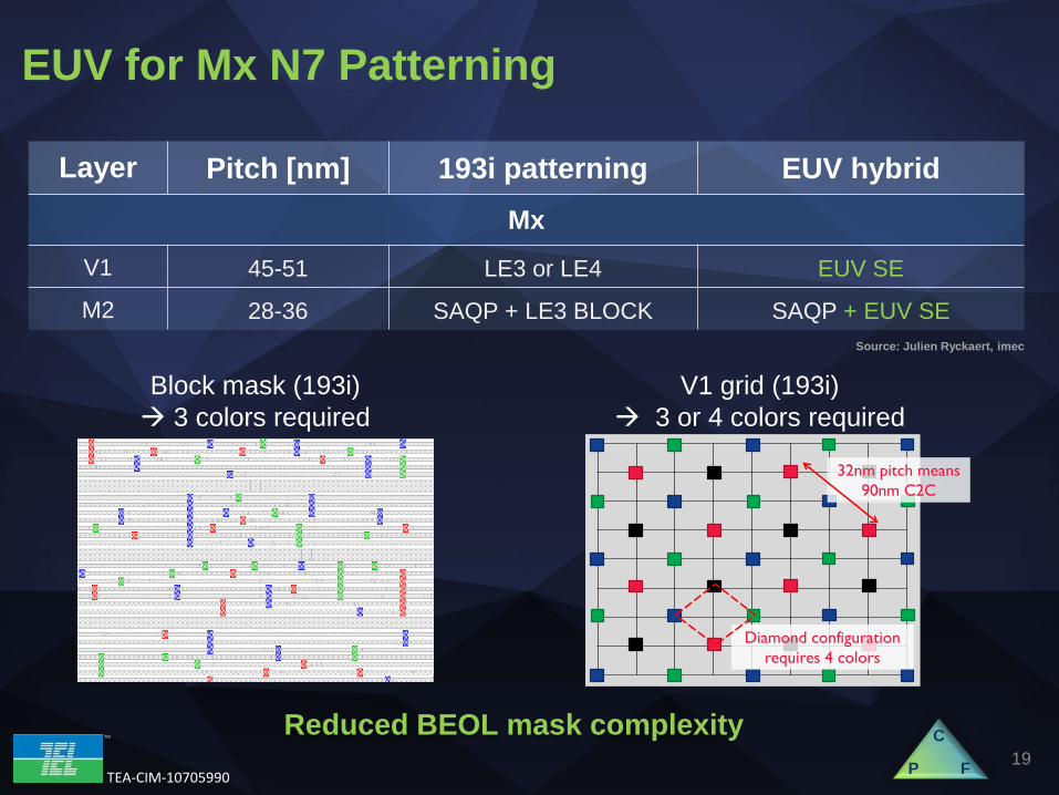
EUV for Mx N7 Patterning
Layer
V1
M2
Pitch [nm]
45-51
28-36
193i patterning
LE3 or LE4
SAQP + LE3 BLOCK
EUV hybrid
EUV SE
SAQP + EUV SE
Mx
32nm pitch means 90nm C2C
Diamond configuration requires 4 colors
Block mask (193i) 3 colors required
V1 grid (193i) 3 or 4 colors required
P
C
F
Reduced BEOL mask complexity
Source: Julien Ryckaert, imec
TM
TEA-CIM-10705990 20
Innovation and Inflection Points
N7 Patterning Trade-offs and Scenarios
Collaborative N7 Patterning R&D
Summary
Market factors, technical backdrop How much trouble are we in???
EUV hybrid vs. iArF only options Cost, Performance, Flexibility
Non-lithographic techniques to assist patterning EUV assisted DSA
Outline
TM
TEA-CIM-10705990
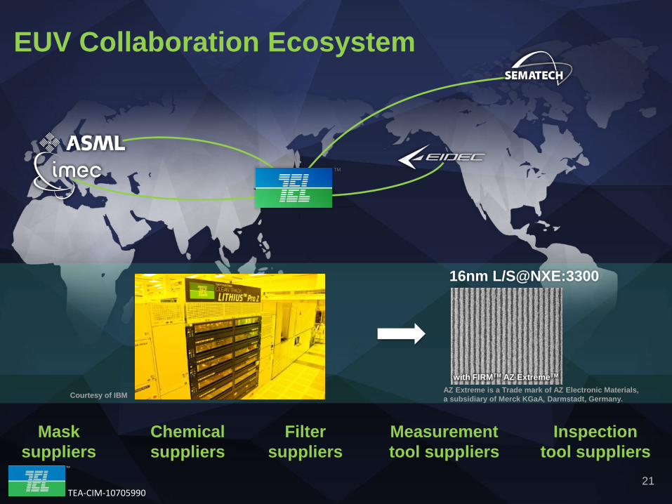
EUV Collaboration Ecosystem
Mask suppliers
Chemical suppliers
Filter suppliers
Measurement tool suppliers
Inspection tool suppliers
with FIRMTM AZ ExtremeTM
16nm L/S@NXE:3300
AZ Extreme is a Trade mark of AZ Electronic Materials, a subsidiary of Merck KGaA, Darmstadt, Germany.
TM
Courtesy of IBM
21
TM
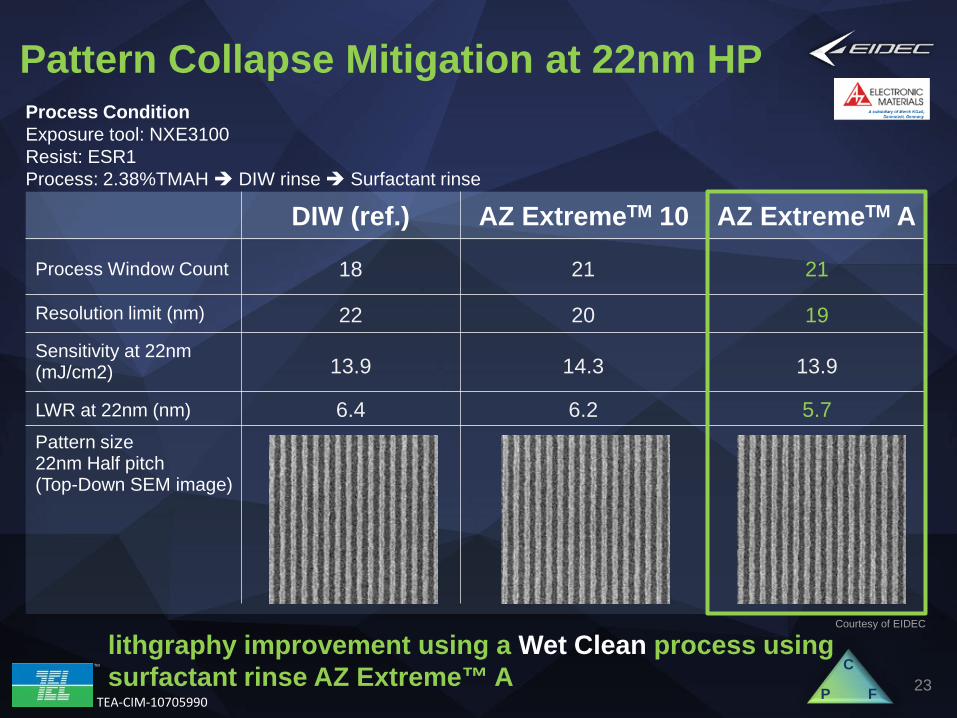
TEA-CIM-10705990 22
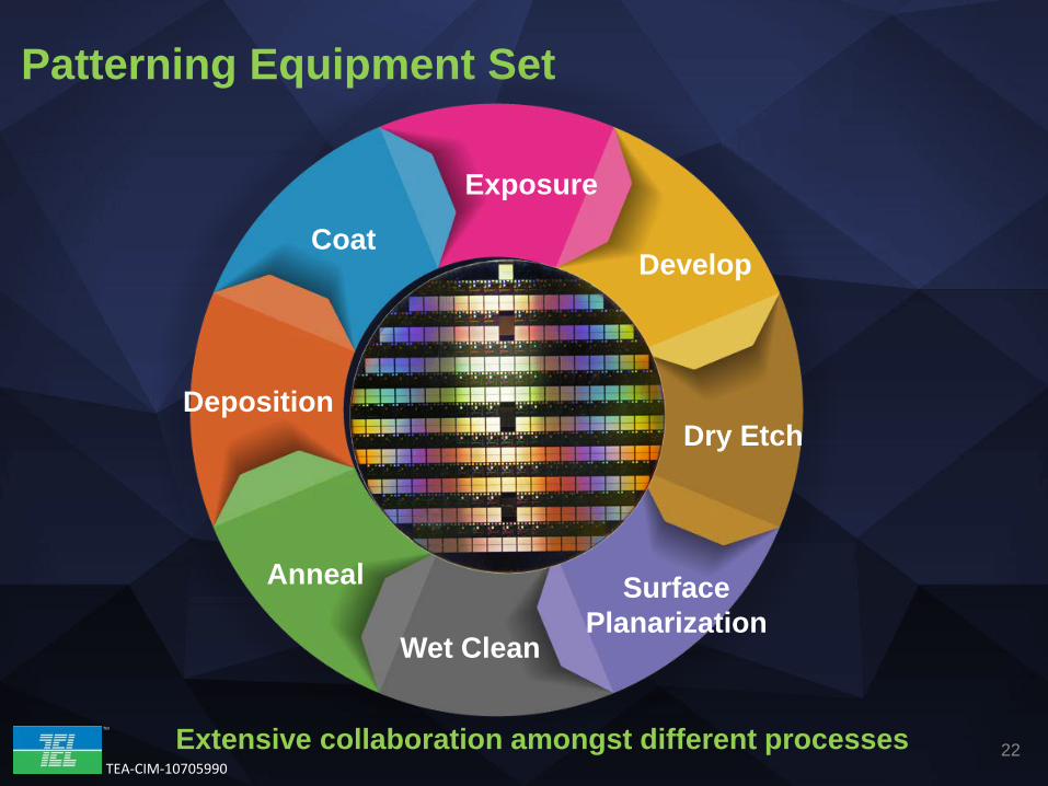
Patterning Equipment Set
Exposure
Develop
Dry Etch
Surface Planarization
Wet Clean
Anneal
Deposition
Coat
Extensive collaboration amongst different processes
TM
TEA-CIM-10705990 23 P
C
F
lithgraphy improvement using a Wet Clean process using surfactant rinse AZ Extreme™ A
Process Condition Exposure tool: NXE3100 Resist: ESR1 Process: 2.38%TMAH DIW rinse Surfactant rinse
Pattern size 22nm Half pitch (Top-Down SEM image)
DIW (ref.) AZ ExtremeTM 10 AZ ExtremeTM A
Courtesy of EIDEC
Process Window Count
Resolution limit (nm)
Sensitivity at 22nm (mJ/cm2)
LWR at 22nm (nm)
18
22
13.9
6.4
21
20
14.3
6.2
21
19
13.9
5.7
Pattern Collapse Mitigation at 22nm HP
TM
TEA-CIM-10705990 24
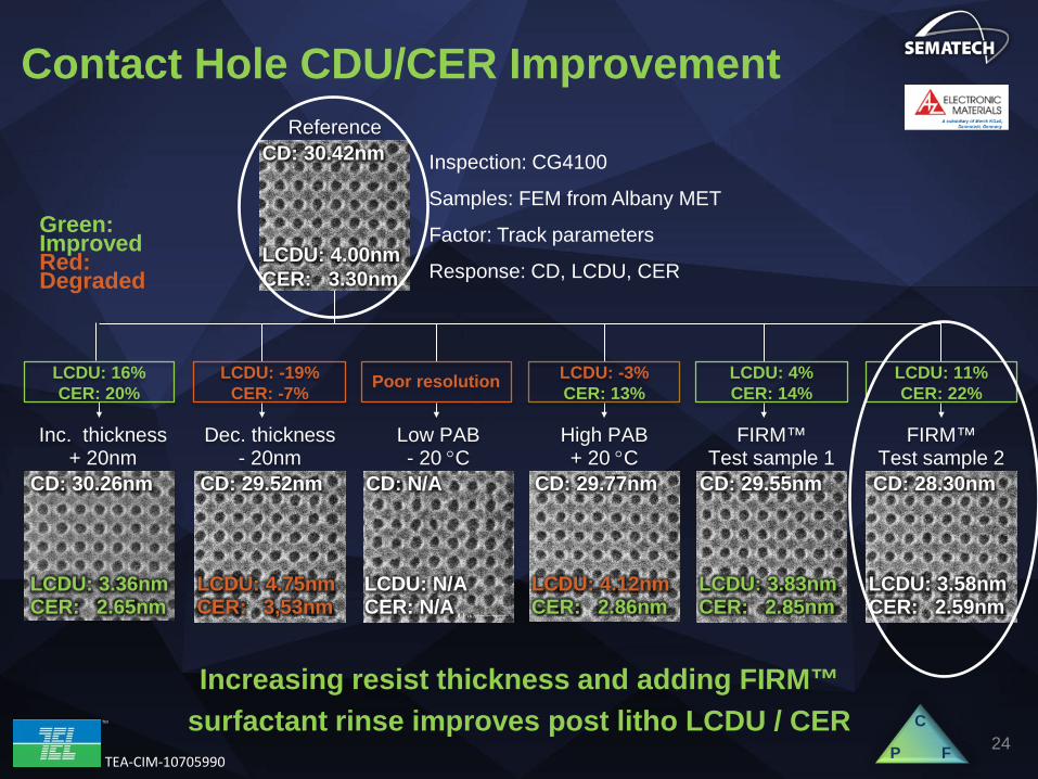
Contact Hole CDU/CER Improvement
LCDU: 4.75nm CER: 3,53nm
LCDU: N/A CER: N/A
LCDU: 4.12nm CER: 2.86nm
LCDU: 3.83nm CER: 2.85nm
LCDU: 3.58nm CER: 2.59nm
Green: Improved Red: Degraded
CD: 30.42nm
LCDU: 4.00nm CER: 3.30nm
LCDU: 3.36nm CER: 2.65nm
Inspection: CG4100
Samples: FEM from Albany MET
Factor: Track parameters
Response: CD, LCDU, CER
P
C
F
CD: 30.26nm CD: 29.52nm CD: N/A CD: 29.77nm CD: 29.55nm CD: 28.30nm
Inc. thickness + 20nm
Dec. thickness - 20nm
Low PAB - 20 °C
High PAB + 20 °C
FIRM™ Test sample 1
FIRM™ Test sample 2
Reference
LCDU: 16% CER: 20%
LCDU: -19% CER: -7% Poor resolution LCDU: -3%
CER: 13% LCDU: 4% CER: 14%
LCDU: 11% CER: 22%
Increasing resist thickness and adding FIRM™ surfactant rinse improves post litho LCDU / CER
TM
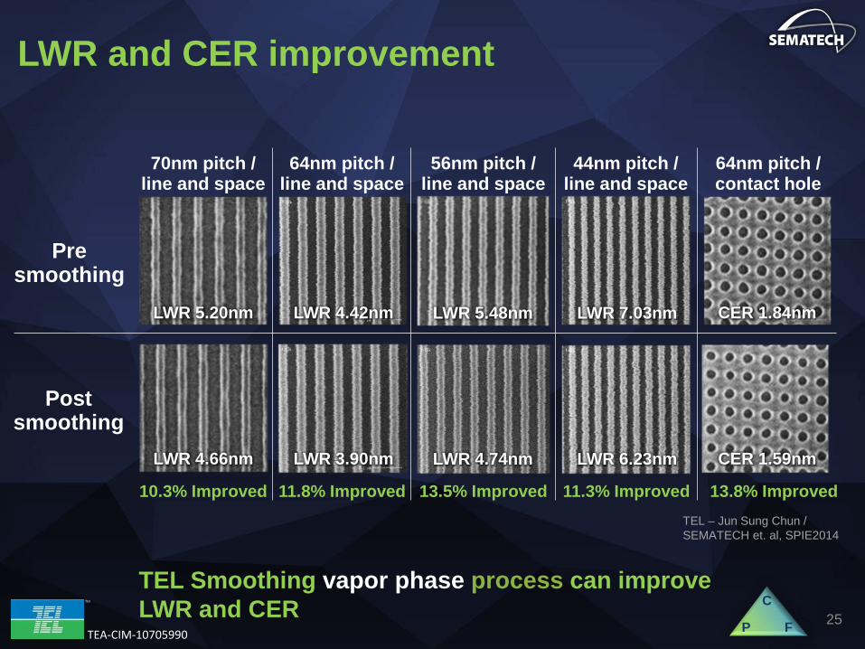
TEA-CIM-10705990 25
Pre smoothing
Post smoothing
TEL Smoothing vapor phase process can improve LWR and CER
LWR and CER improvement
LWR 5.20nm LWR 4.42nm LWR 5.48nm LWR 7.03nm CER 1.84nm
LWR 4.66nm LWR 3.90nm LWR 4.74nm LWR 6.23nm CER 1.59nm
10.3% Improved 11.8% Improved 13.5% Improved 11.3% Improved 13.8% Improved
70nm pitch / line and space
64nm pitch / line and space
56nm pitch / line and space
44nm pitch / line and space
64nm pitch / contact hole
TEL – Jun Sung Chun / SEMATECH et. al, SPIE2014
P
C
F
TM
TEA-CIM-10705990 26
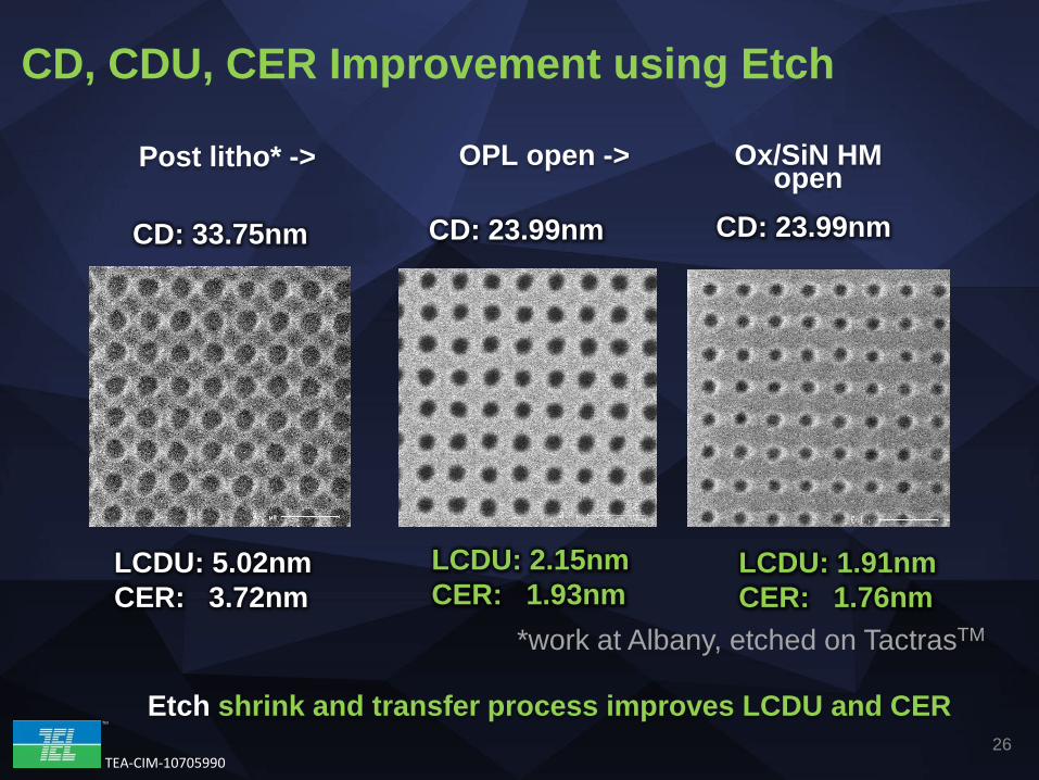
CD, CDU, CER Improvement using Etch
Post litho* -> OPL open -> Ox/SiN HM open
LCDU: 5.02nm CER: 3.72nm
CD: 33.75nm
Etch shrink and transfer process improves LCDU and CER
LCDU: 2.15nm CER: 1.93nm
CD: 23.99nm
LCDU: 1.91nm CER: 1.76nm
CD: 23.99nm
*work at Albany, etched on TactrasTM
TM
TEA-CIM-10705990
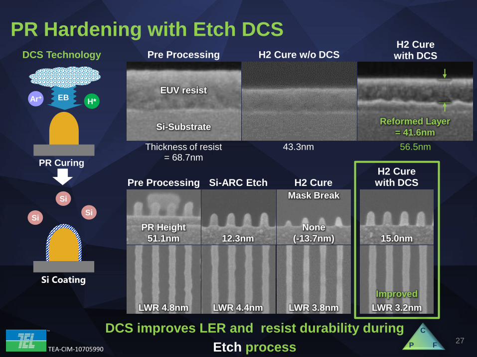
PR Hardening with Etch DCS
27
Si-Substrate
EUV resist
Reformed Layer = 41.6nm
Thickness of resist = 68.7nm
Pre Processing H2 Cure w/o DCS
H2 Cure with DCS
43.3nm 56.5nm
LWR 4.8nm LWR 4.4nm LWR 3.2nm Improved
LWR 3.8nm
Pre Processing Si-ARC Etch H2 Cure H2 Cure with DCS
PR Height 51.1nm 12.3nm 15.0nm
None (-13.7nm)
Mask Break
P
C
F
DCS Technology
H* Ar+ EB
Si Si Si
PR Curing
Si Coating
DCS improves LER and resist durability during Etch process
TM
TEA-CIM-10705990
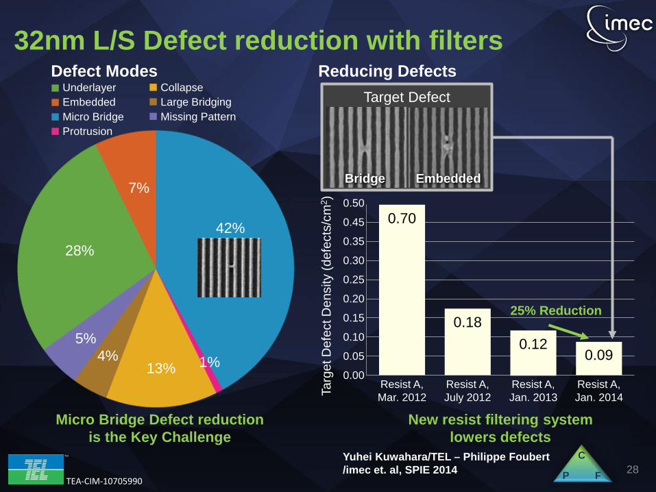
Defect Modes Underlayer Embedded Micro Bridge Protrusion
Collapse Large Bridging Missing Pattern
42%
1% 13% 4%
5%
28%
7%
Micro Bridge Defect reduction is the Key Challenge
New resist filtering system lowers defects
Reducing Defects
Targ
et D
efec
t Den
sity
(def
ects
/cm
2 )
0.50
0.45
0.35
0.30
0.25
0.20
0.15
0.10
0.05
0.00
Resist A, Mar. 2012
Resist A, July 2012
Resist A, Jan. 2013
Resist A, Jan. 2014
0.70
0.18 0.12
0.09
25% Reduction
Target Defect
Bridge Embedded
32nm L/S Defect reduction with filters
28 P
C
F
Yuhei Kuwahara/TEL – Philippe Foubert /imec et. al, SPIE 2014
TM
TEA-CIM-10705990
37%
2% 19%
29%
9%
Underlayer/SI Embedded Partially closed hole
Particle Residue Large irregular bridging
4%
Reducing Defects
Def
ect D
ensi
ty (d
efec
ts/c
m2 )
2.5
2.0
1.5
1.0
0.5
0.0
April 2013 Resist E
EUVL 2013 Resist E
SPIE 2014 Resist E
0.88
0.54 0.44
2.24
0.32
0.86
0.09
0.54
Underlayer/SI Embedded Residue
1.37
Residue Defect reduction is the key Challenge
New rinse technique reduces defects
Defect Modes 30nm CH Defect reduction through rinse
29 Yuhei Kuwahara/TEL – Philippe Foubert /imec et. al, SPIE 2014
Others Residue
P
C
F
37% Reduction
TM
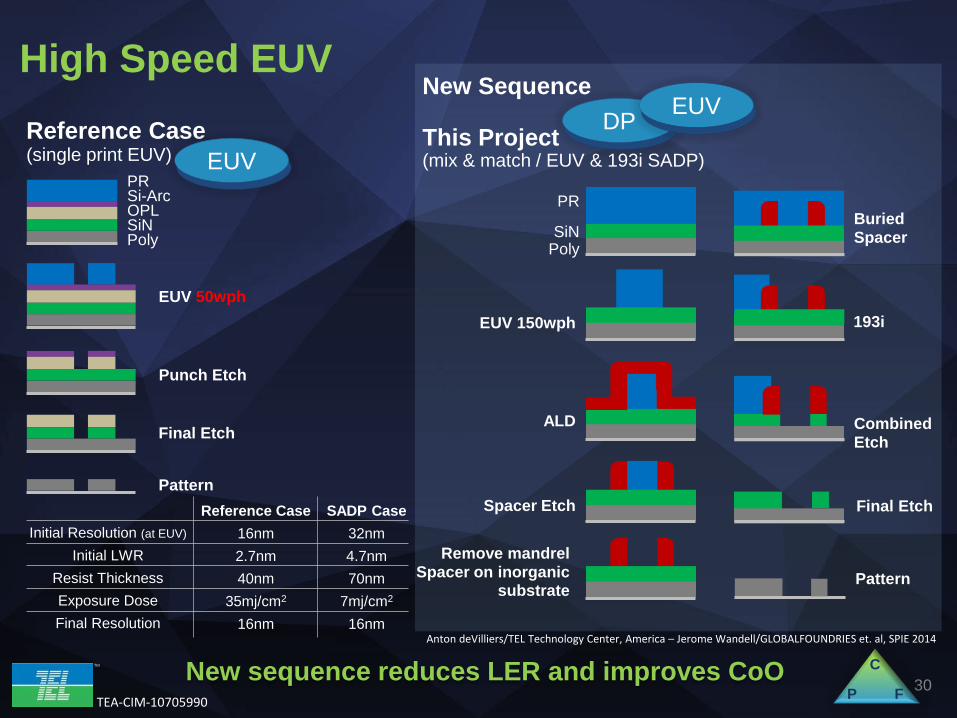
TEA-CIM-10705990 30
High Speed EUV
This Project PR Si-Arc OPL SiN Poly
Reference Case
EUV 50wph
Punch Etch
Final Etch
Pattern
DP EUV DP DP DP EUV
(single print EUV) (mix & match / EUV & 193i SADP)
Initial Resolution (at EUV)
Initial LWR Resist Thickness Exposure Dose Final Resolution
Reference Case 16nm 2.7nm 40nm
35mj/cm2
16nm
SADP Case 32nm 4.7nm 70nm
7mj/cm2
16nm
New Sequence
SiN Poly
EUV 150wph
PR
ALD
Spacer Etch
Remove mandrel Spacer on inorganic
substrate
Final Etch
Combined Etch
P
C
F
Pattern
Buried Spacer
193i
New sequence reduces LER and improves CoO Anton deVilliers/TEL Technology Center, America – Jerome Wandell/GLOBALFOUNDRIES et. al, SPIE 2014
TM
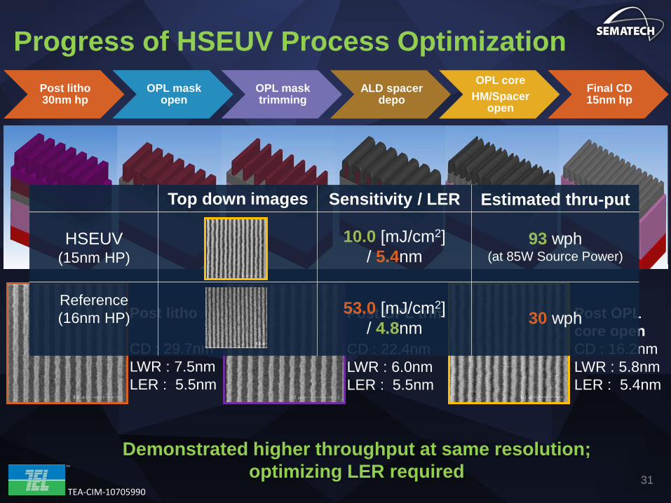
TEA-CIM-10705990 31
Progress of HSEUV Process Optimization Post litho 30nm hp
OPL mask open
OPL mask trimming
ALD spacer depo
OPL core HM/Spacer
open
Final CD 15nm hp
Demonstrated higher throughput at same resolution; optimizing LER required
Post litho CD : 29.7nm LWR : 7.5nm LER : 5.5nm
Post OPL trim CD : 22.4nm LWR : 6.0nm LER : 5.5nm
Post OPL core open CD : 16.2nm LWR : 5.8nm LER : 5.4nm
Top down images Sensitivity / LER Estimated thru-put
10.0 [mJ/cm2] / 5.4nm
53.0 [mJ/cm2] / 4.8nm
93 wph (at 85W Source Power)
30 wph
HSEUV (15nm HP)
Reference (16nm HP)
TM
TEA-CIM-10705990 32
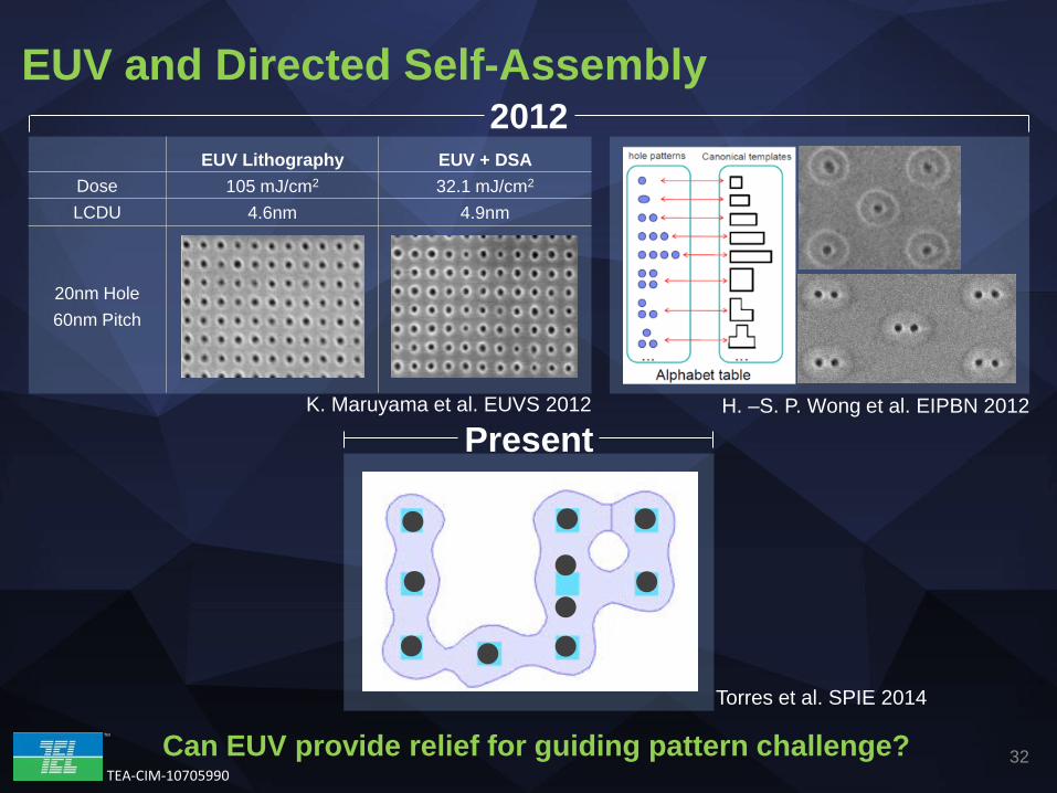
EUV and Directed Self-Assembly
Dose LCDU
EUV Lithography 105 mJ/cm2
4.6nm
EUV + DSA 32.1 mJ/cm2
4.9nm
20nm Hole 60nm Pitch
K. Maruyama et al. EUVS 2012 H. –S. P. Wong et al. EIPBN 2012
Torres et al. SPIE 2014
2012
Present
Can EUV provide relief for guiding pattern challenge?
TM
TEA-CIM-10705990 33
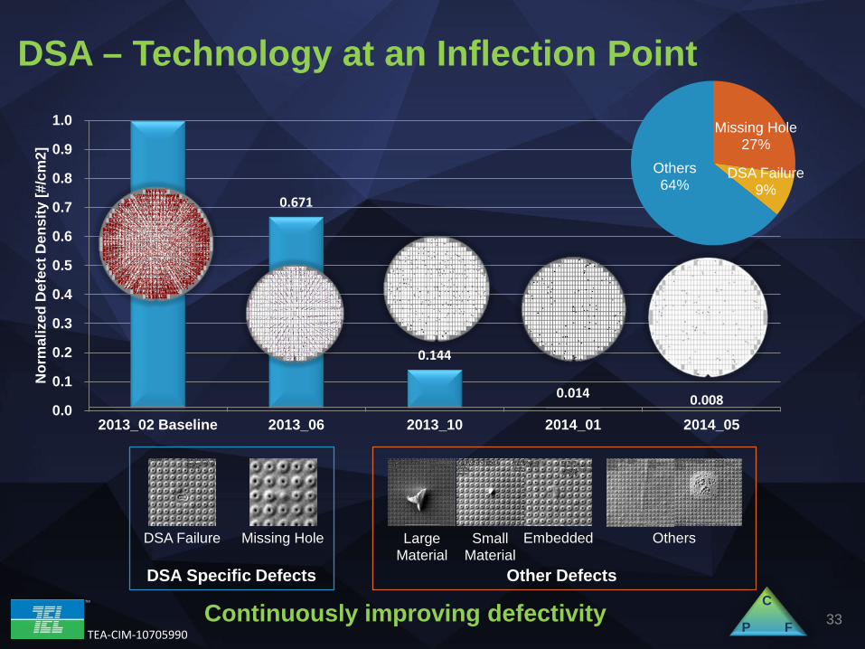
DSA – Technology at an Inflection Point
0.671
0.144
0.014 0.008 0.0
0.1
0.2
0.3
0.4
0.5
0.6
0.7
0.8
0.9
1.0
2013_02 Baseline 2013_06 2013_10 2014_01 2014_05
Nor
mal
ized
Def
ect D
ensi
ty [#
/cm
2]
Missing Hole DSA Failure
Other Defects DSA Specific Defects
Large Material
Small Material
Embedded Others
P
C
F Continuously improving defectivity
Missing Hole 27%
DSA Failure 9%
Others 64%

TM
TEA-CIM-10705990 34
TM
TEA-CIM-10705990 35
Summary
Key challenges for N7 patterning are reducing cost, improving EPE and increasing design flexibility
Convergence of EUV and MP technologies could offer the EPE and flexibility advantages of each approach with reduced cost
IDM/fabless design community collaboration essential to help make choices between patterning tradeoffs
TM
TEA-CIM-10705990 36
Upcoming EUVL Progress Reports
International Symposium on EUVL Impact of Novel Defect Reduction Hardware on EUV Patterning Defectivity – Yuhei Kuwahara, TEL Novel Processing Approaches to Enable EUV Lithography toward High Volume Manufacturing – Cecilia Montgomery, SEMATECH, TEL, et al.
TM
TEA-CIM-10705990 37
Acknowledgements Semiconductor companies’ collaborations Consortia (EIDEC, imec, SEMATECH) Material suppliers (AZEM, et al.) EDA vendors (Mentor) Equipment suppliers (ASML, HHT, KLA-Tencor) TELTM global technology teams (LPDC, TDC, ATG, TTCA)
Co-authors
Hidetami Yaegashi Kenichi Oyama Takahiro Kitano Makoto Muramatsu Kousuke Yoshihara Satoru Shimura Shinichiro Kawakami Toshikatsu Tobana
Steven Scheer Carlos Fonseca Ben Rathsack Anton deVilliers Serge Biesmans
Koichi Yatsuda Ken Nawa Noritaka Yokomori Hideo Nakashima Seiji Nagahara Hiroyuki Iwaki Akihiro Sonoda Makiko Dojun


![EUVL Symposium HVM FINAL 2004[1]](https://img.pdfslide.us/doc/110x75/55c513d9bb61ebc37e8b4574/euvl-symposium-hvm-final-20041.jpg)