Embed Size (px)
Citation preview
Operating Organic Electronics via
Aqueous Electric Double Layers
Henrik Toss
Norrköping 2015
Operating Organic Electronics via Aqueous Electric Double
Layers
Henrik Toss
During the course of the research underlying this thesis, Henrik Toss was
enrolled in Forum Scientium, a multidisciplinary doctoral program at
Linköping University, Sweden.
Linköping Studies in Science and Technology. Dissertation No. 1704 Copyright © Henrik Toss, 2015, unless otherwise noted Cover by Henrik Toss Printed by LiU-Tryck, Linköping, Sweden, 2015 ISBN 978-91-7685-944-5 ISSN 0345-7524 Electronic publication: http://www.ep.liu.se
Abstract
The field of organic electronics emerged in the 1970s with the
discovery of conducting polymers. With the introduction of plastics
as conductors and semiconductors came many new possibilities both
in production and function of electronic devices. Polymers can often
be processed from solution and their softness provides both the
possibility of working on flexible substrates, and various advantages
in interfacing with other soft materials, e.g. biological samples and
specimens. Conducting polymers readily partake in chemical and
electrochemical reactions, providing an opportunity to develop new
electrochemically driven devices, but also posing new problems for
device engineers.
The work of this thesis has focused on organic electronic devices
in which aqueous electrolytes are an active component, but still
operating in conditions where it is desirable to avoid electrochemical
reactions. Interfacing with aqueous electrolytes occurs in a wide
variety of settings, but we have specifically had biological
environments in mind as they necessarily involve the presence of
water. The use of liquid electrolytes also provides the opportunity to
deliver and change the device electrolyte continuously, e.g. through
microfluidic systems, which could then be used as a dynamic feature
and/or be used to introduce and change analytes for sensors. Of
particular interest is the electric double layer at the interface
between the electrolyte and other materials in the device, specifically
its sensitivity to charge reorganization and high capacitance.
The thesis first focuses on organic field effect transistors gated
through aqueous electrolytes. These devices are proposed as
biosensors with the transistor architecture providing a direct
transduction and amplification so that it can be electrically read out.
It is discussed both how to distinguish between the various operating
mechanisms in electrolyte thin film transistors and how to choose a
strategy to achieve the desired mechanism. Two different strategies
to suppress ion penetration into, and thus electrochemical doping of,
the organic semiconductor are presented.
The second focus of the thesis is on polarization of ferroelectric
polymer films through electrolytes. A model for the interaction
between the remnant ferroelectric charge in the polymer film and the
mobile ionic charges of the electrolyte is presented, and verified
experimentally. The reorientation of the ferroelectric polarization via
the electric double layer is also demonstrated in a regenerative
medicine application; the ferroelectric polarization is shown to affect
cell binding, and is used as a gentle method to non-destructively
detach cells from a culture substrate.
Populärvetenskaplig Sammanfattning
Upptäckten av ledande polymerer på 1970-talet blev startskottet
för forskningsområdet ledande plaster och senare också för organisk
elektronik. Möjligheten att använda polymera material, det vill säga
plaster, som elektrisk ledare och halvledare i elektroniska
komponenter innebär en rad olika fördelar med avseende på
processteknik för tillverkning av komponenter och kretsar, men
öppnar också upp för helt nya elektroniska komponenter och
användningsområden. De organiska elektronikmaterialen går ofta att
enkelt lösa upp i lösningsmedel och dessa lösningar kan användas för
tillverkning som utnyttjar till exempel traditionella tryck- eller
bestrykningsmetoder. De är relativt mjuka och elastiska vilket
innebär att materialen kan användas på flexibla substrat och ofta
passar bättre, inte minst rent mekaniskt, ihop med andra mjuka
system, exempelvis biologiska system eller som elektronik på
papper. Ofta är de ledande och halvledande polymererna
elektrokemiskt aktiva vilket också möjliggör utveckling av helt nya
komponenter och applikationer.
Arbetet som ligger till grund för denna avhandling har fokuserats
emot att nyttja vattenbaserade elektrolyter i kombination med
elektroniska komponenter baserade på polymerer för att realisera
nya sensorer och aktuatorer för tillämpningar inom medicin och
bioteknologi. Syftet är att utnyttja elektroniska funktioner i dessa
komponenter för att detektera, karakterisera och reglera processer i
biologiska system, samtidigt som elektrokemiska reaktioner
undertrycks. I biologiska system och miljöer är i normalfallet vatten
närvarande vilket både innebär en möjlighet men samtidigt en
utmaning. Vid gränsskiktet mellan elektrolyter och andra
elektroaktiva material bildas ett elektriskt dubbellager av laddningar
vilket i sin tur innebär att vi kan erhålla mycket höga kapacitanser.
Egenskaperna utmed och i det elektriska dubbellagret är mycket
känsligt för små förändringar av orientering och struktur av de

inkluderade laddningarna. Denna egenskap kan utnyttjas som en
känslig och eventuellt selektiv reaktionsmekanism i olika sensorer
och aktuatorer. Då elektrolyten kan representeras av olika biologiska
system och vätskor öppnas en rad olika möjligheter med inom
biologi och medicin.
Organiska fälteffekttransistorer vilka inkluderar elektriska
dubbellager som isolator för styret kan användas som sensorer där
transistorstrukturen både kan överföra och förstärka en sensorsignal
till en elektriskt mätbar signal. För en tydlig signal i sådana
fälteffektkomponenter krävs ofta att elektrokemiska (sido-
)reaktioner undviks eller undertrycks. I denna avhandling diskuteras
och realiseras två olika strategier för att undertrycka penetration av
joner från elektrolyten in i de polymera elektronikmaterialen för att
minimera att sensorsignalen går förlorad i elektrokemiska signaler.
Den laddning som kan lagras i det elektriska dubbellagret används
också till att polarisera tunna ferroelektriska polymerfilmer.
Samspelet och kopplingen mellan laddningen i det elektriska
dubbellagret och de ferroelektriska dipolerna i polymeren
modelleras och simuleras för att förstå och möjliggöra nya
användningsområden inom bioteknologi. Beroende på orienteringen
av de ferroelektriska dipolerna så kan affinitet och frisättning av
levande celler till den ferroelektriska polymerytan styras helt
elektroniskt. Detta öppnar nya möjligheter med så kallade
elektroniska odlingsskålar inom regenerativ medicin samt inom
biologi.
Acknowledgments
This thesis would not have been possible to realize without the help
and support from the people around me. I would especially like to
express my sincere gratitude to:
Magnus Berggren, my main supervisor, for providing me the
opportunity to work in the Laboratory of Organic Electronics.
Edwin Jager, my first co-supervisor, for introducing me to the field
of organic bioelectronics.
Daniel Simon, my second co-supervisor, for all the support, advice
and interesting discussions and for sharing your insights in
bioelectronics.
Sophie Lindesvik, for all the help with everything and anything even
remotely related to administration.
Åsa Wallhagen, for administrative help during my final months as a
PhD student.
Magnus Glänneskog for putting me in contact with some of the right
people at the right time.
Lasse Gustavsson, Bengt Råsander, Anna Malmström, Putte
Eriksson and everyone else keeping the lab up and running.
Past and present members of the Laboratory of Organic
Electronics. In particular Lars and Anders for introducing me to the
lab, Ari for your invaluable inputs on processing, my amazing office
mates Kristin, Amanda and Negar making me never wish for an
office of my own, Malti for the gym sessions and intense discussions,
and “The Prästgatan Girls” Donata, Ellen and Dan for hosting both
me and the best parties in Norrköping.

All the co-authors of the included papers, especially Serafina
Cotrone and Clément Suspène for the very intense lab sessions and
scientific discussions, and Susanna Lönnqvist for testing my devices
with cells.
Staff of Acreo Norrköping. Especially David Nilsson, Anurak
Sawatdee and Xin Wang for all your help and valuable discussions.
Annelie Eveborn and Olle-Jonny Hagel at Thin Film Electronics for
all the useful tips on processing.
Forum Scientium and Stefan Klinström for the great research trips.
My parents Anna and Per, my brother Martin and sister Elin, and
my fantastic in-laws Hasse, Ylva and Åsa for all the love and support.
My Love, Anna, who has shared in my frustration and joy over these
years, knows me better than anyone and still stays by my side; your
love and support means more to me than words can describe. Our
Karin, who makes me realize what is truly important in life.
List of Included Papers
Paper I
On the mode of operation in electrolyte-gated thin film
transistors based on different substituted polythiophenes
Henrik Toss, Clément Suspène, Benoît Piro, Abderrahim Yassar,
Xavier Crispin, Loïg Kergoat, Minh-Chau Pham, and Magnus Berggren
Organic Electronics 15, pp. 2420–2427 (2014)
Contribution: Designed experiments, performed most of the
experimental work, wrote most of the manuscript.
Paper II
Copolythiophene-based water-gated organic field-effect
transistors for biosensing
Clément Suspène, Benoit Piro, Steeve Reisberg, Minh-Chau Pham,
Henrik Toss, Magnus Berggren, Abderrahim Yassar, and Gilles
Horowitz
Journal of Materials Chemistry B 1, pp. 2090-2097 (2013)
Contribution: Fabrication and electrical characterization of devices,
wrote part of the manuscript and contributed to the editing of the
final manuscript.
Paper III
Phospholipid film in electrolyte-gated organic field-effect
transistors
Serafina Cotrone, Marianna Ambrico, Henrik Toss, M. Daniela
Angione, Maria Magliulo, Antonia Mallardi, Magnus Berggren,
Gerardo Palazzo, Gilles Horowitz, Teresa Ligonzo, and Luisa Torsi
Organic Electronics 13, pp. 638–644 (2012)
Contribution: Fabrication and electrical characterization of devices,
contributed to experimental design, initial analysis of data, wrote
part of the manuscript and contributed to the editing of the final
manuscript.
Paper IV
Polarization of ferroelectric films through electrolyte
Henrik Toss, Negar Sani, Simone Fabiano, Daniel T Simon, Robert
Forchheimer, and Magnus Berggren
Manuscript in preparation
Contribution: Created models, wrote simulation protocols, designed
experiments, performed most of the experimental work and wrote
most of the manuscript.

Paper V
Ferroelectric Surfaces for Cell Release
Henrik Toss, Susanna Lönnqvist, David Nilsson, Anurak Sawatdee,
Josefin Nissa, Simone Fabiano, Magnus Berggren, Gunnar Kratz, and
Daniel T. Simon
Submitted manuscript
Contribution: Contributed to experiment design, fabrication and
electrical characterization of devices, wrote the first draft and
contributed to editing of the final manuscript
Table of Contents
1. INTRODUCTION ................................................................................... 1
1.1 ORGANIC ELECTRONICS ......................................................................... 1
1.2 AIM AND OUTLINE OF THE THESIS ............................................................ 2
2. MATERIALS .......................................................................................... 5
2.1 ORGANIC SEMICONDUCTORS .................................................................. 5
2.1.1 Orbitals ................................................................................... 6
2.1.2 Hybridization .......................................................................... 8
2.1.3 Electronic structure of conjugated polymers .......................... 9
2.1.4 Charge carriers ..................................................................... 11
2.1.5 Doping .................................................................................. 12
2.2 POLARITY OF MOLECULES ..................................................................... 13
2.2.1 Electronegativity ................................................................... 13
2.2.2 Dielectric polarization ........................................................... 13
2.3 ELECTROLYTES ................................................................................... 14
2.3.1 Electric double layer ............................................................. 15
3. DEVICES ............................................................................................. 17
3.1 CAPACITORS ...................................................................................... 17
3.1.1 Electric double layer capacitors ............................................ 18
3.1.2 Super capacitors ................................................................... 19
3.1.3 Pseudo capacitors ................................................................. 20
3.2 TRANSISTORS .................................................................................... 20
3.2.1 Thin film transistors .............................................................. 21
3.2.2 Field effect transistors .......................................................... 21
3.2.3 Transistor operation ............................................................. 22
3.2.4 Electrochemical transistors................................................... 27
3.2.5 Electrolyte gated thin film transistor sensors ....................... 29
3.3 FERROELECTRIC SURFACES .................................................................... 33
4. EXPERIMENTAL METHODS ................................................................. 35
4.1 FABRICATION ..................................................................................... 35
4.1.1 Thermal evaporation ............................................................ 35
4.1.2 Photolithography .................................................................. 36
4.1.3 Spin coating .......................................................................... 37
4.1.4 Typical fabrication of devices used in this thesis .................. 38
4.2 CHARACTERIZATION ............................................................................ 39
4.2.1 Current-Voltage measurements ........................................... 39
4.2.2 Impedance spectroscopy ...................................................... 40
5. BASIC CELL BIOLOGY .......................................................................... 45
5.1 CELLS ............................................................................................... 45
5.2 PHOSPHOLIPIDS AND THE CELL MEMBRANE .............................................. 46
5.3 MEMBRANE PROTEINS ........................................................................ 47
5.4 EXTRACELLULAR MATRIX ...................................................................... 47
5.5 BINDING PROTEINS/MECHANISMS ......................................................... 48
5.6 BIORECOGNITION EVENTS .................................................................... 48
5.7 CELL DETACHMENT ............................................................................. 48
6. CONCLUSIONS AND FUTURE OUTLOOK ............................................. 51
REFERENCES .............................................................................................. 55

“Remember kids; the only difference between
screwing around and science is writing it down”
- Adam Savage

Part I
Background

1
1. Introduction
1.1 Organic Electronics
Electronics represent a corner stone in modern society and is
integrated and represented into almost every aspect of our lives. This
appears as a natural continuation of the early electronic era that
started in 1947 with the invention of the first transistor achieved by
John Bardeen and Walter Brattain at Bell Laboratories [1], USA.
The transistor enabled the further development of great many
applications and technologies; most notably the computer science
era, and the transistor device is now the basic building block of all
modern electronics. To make transistor-based technologies various
inorganic materials have traditionally been used, such as metal
conductors and silicon and geranium as semiconductors.
Polymer materials, commonly known as plastics, were for a long
time considered to only be insulators with respect to electrical
current. This view changed in the late 1970s when Alan Heeger, Alan
MacDiarmid and Hideki Shirakawa discovered that the conductivity
of polyacetylene could be improved through chemical doping [2]. It is
the alternating single and double chemical bond-structure of
2
polyacetylene and other so called conjugated polymers that gives
them their conducting properties [3]. This discovery marks the
starting point of the scientific field of conducting polymers, which
then led also to the area known as organic electronics.
Polymers are easily processed and can be tailored to carry and
represent a vast range of different chemical and mechanical
properties. By just glancing at the examples of the synthetic fibers
and acrylic glasses gives a hint to the range of applications in which
we can find polymeric materials today.
Organic electronic materials combine the desired processability of
polymers with the electrical and optical features of metals and
semiconductors. Classic semiconductor devices such as Light
Emitting Diodes (LEDs) [4], Field Effect Transistors (FETs) [5-6] and
solar cells [7-10] including electronic polymers as the semiconductor
have already been developed. Moreover, some of the organic
semiconductors (OSC) are also electrochemically active, which
enables the development of organic electrochemical transistors
(OECTs) [11], super capacitors [12-13], electrochromic display cells [14-15]
and light emitting electrochemical cells (LECs) [16-17]. In addition,
organic materials express several unique features making them
suitable for biological and biochemical applications. They are
relatively soft and can be made to be both electronically and ionically
conductive [18]. These features make them excellent as the interface
between technology and soft living materials both for recording as
well as transmitting signals in biology, and potentially also in
medicine.
1.2 Aim and outline of the thesis
In all sensor or actuator systems some kind of transducer is
needed to translate and/or interpret the signals from one end of the
system to the other. As electronics are becoming a more and more
integral part of our lives, and in technology, it is desired to utilize
electrical transduction mechanisms as it would open up for the
possibility of a direct interfacing, including that of electronics, that
Introduction
3
record or control biological signal patterns. As mentioned above,
organic electronics appears to be a very good fit with respect to
interfacing with many biological and biochemical systems. Water is a
fundamental component of life as we know it and will thus be present
in many of these systems. With this, both challenges and
opportunities arise. Electrically active devices operating in aqueous
environment results in that charge polarization is established along
the active interfaces. This might, in turn, result in electrochemical
side-reactions. Depending on the design, of a sensor or actuator in
question, the electrochemical reactions can be desired or not. In any
case, it is crucial to understand the characteristics along the
electronic-aqueous interface in order to fully be able to control,
predict and understand the behavior of these types of devices while
operating as a sensor or actuator.
The first part of this thesis serves as an introduction and a brief
summary of the background information needed to understand the
scientific findings presented in the papers and manuscripts, included
in the second part of the thesis.

5
2. Materials
2.1 Organic semiconductors
Polymers are linear macromolecules built up by, as the name
suggests, many (Poly) repeating subunits (mers) connected by
covalent bonds. For a long time polymers were considered being only
electronic insulators as this is the case for many of the more common
polymers or plastics we encounter. However, in 1977 Alan Heeger,
Hideki Shirakawa and Alan G MacDiarmid reported the possibility to
enhance the conductivity of the polymer polyacetylene by exposing it
to iodine vapor [2]. With this experiment, they discovered that
polymers with an alternating single and double bond structure, i.e.
conjugated polymers, could be made electronically conductive due to
their molecular structure. This finding was then the starting point of
two completely new fields of research – Conducting Polymers and
Organic Electronics.
6
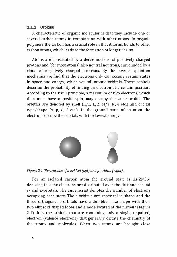
2.1.1 Orbitals A characteristic of organic molecules is that they include one or
several carbon atoms in combination with other atoms. In organic
polymers the carbon has a crucial role in that it forms bonds to other
carbon atoms, which leads to the formation of longer chains.
Atoms are constituted by a dense nucleus, of positively charged
protons and (for most atoms) also neutral neutrons, surrounded by a
cloud of negatively charged electrons. By the laws of quantum
mechanics we find that the electrons only can occupy certain states
in space and energy, which we call atomic orbitals. These orbitals
describe the probability of finding an electron at a certain position.
According to the Pauli principle, a maximum of two electrons, which
then must have opposite spin, may occupy the same orbital. The
orbitals are denoted by shell (K/1, L/2, M/3, N/4 etc.) and orbital
type/shape (s, p, d, f etc.). In the ground state of an atom the
electrons occupy the orbitals with the lowest energy.
Figure 2.1 Illustrations of s-orbital (left) and p-orbital (right).
For an isolated carbon atom the ground state is 1s22s22p2
denoting that the electrons are distributed over the first and second
s- and p-orbitals. The superscript denotes the number of electrons
occupying each state. The s-orbitals are spherical in shape and the
three orthogonal p-orbitals have a dumbbell like shape with their
two ellipsoid shaped lobes and a node located at the nucleus (Figure
2.1). It is the orbitals that are containing only a single, unpaired,
electron (valence electrons) that generally dictate the chemistry of
the atoms and molecules. When two atoms are brought close

Materials
7
together the orbitals of the valence electrons can start to overlap and
form a chemical bond due to interactions between valence electrons.
The resulting molecular orbitals can be approximated as linear
combinations of the two atomic orbitals and their nature depend on
the properties of, and the relationship, between the involved atomic
orbitals. If the bond is symmetrical, with respect to the rotational axis
of the bond, it is called a σ-bond (Figure 2.2). If the resulting bond is
not symmetrical it is called a π-bond. Furthermore, the energy levels
of the combined atomic orbitals can split into a bonding and an
antibonding molecular orbital. The resulting energy of a bonding
orbital, of a molecule, is lower than the energy of the individual
atomic orbitals and thus stabilizes the molecule, while the
antibonding orbital has a relatively higher energy than the atomic
orbitals and expresses destabilizing characteristics. The antibonding
orbitals are often denoted with an asterix (σ*, π*). A lower binding
energy level indicates a stronger molecular bond and, as indicated by
the name, the bonding orbitals thus have lower energy than the
antibonding. The overlap between atomic orbitals is generally larger
in a σ-bond than in the corresponding π-bond and the energy of the
σ-bond is thus often lower in energy. In the ground state the
electrons will occupy the orbitals with the lowest energy. The
molecular orbital, with the highest energy, occupied by an electron is
called the Highest Occupied Molecular Orbital (HOMO). The
molecular orbital, without electrons, with the lowest energy is called
the Lowest Unoccupied Molecular Orbital (LUMO) [19].
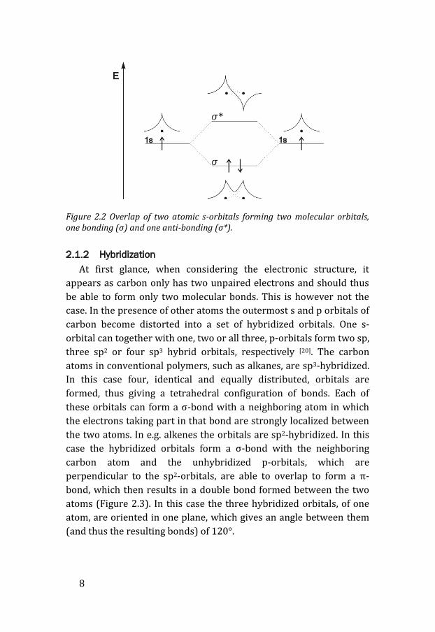
8
Figure 2.2 Overlap of two atomic s-orbitals forming two molecular orbitals, one bonding (σ) and one anti-bonding (σ*).
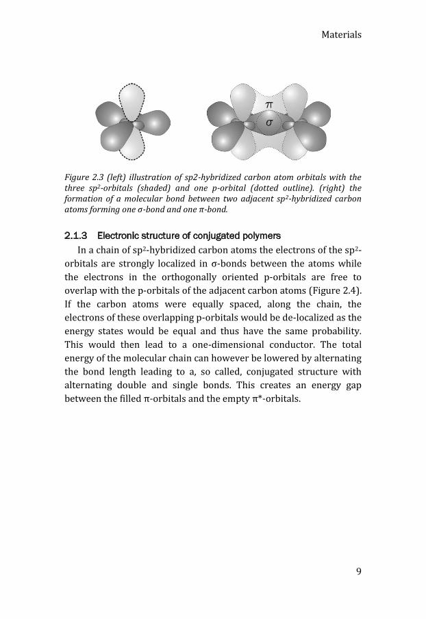
2.1.2 Hybridization At first glance, when considering the electronic structure, it
appears as carbon only has two unpaired electrons and should thus
be able to form only two molecular bonds. This is however not the
case. In the presence of other atoms the outermost s and p orbitals of
carbon become distorted into a set of hybridized orbitals. One s-
orbital can together with one, two or all three, p-orbitals form two sp,
three sp2 or four sp3 hybrid orbitals, respectively [20]. The carbon
atoms in conventional polymers, such as alkanes, are sp3-hybridized.
In this case four, identical and equally distributed, orbitals are
formed, thus giving a tetrahedral configuration of bonds. Each of
these orbitals can form a σ-bond with a neighboring atom in which
the electrons taking part in that bond are strongly localized between
the two atoms. In e.g. alkenes the orbitals are sp2-hybridized. In this
case the hybridized orbitals form a σ-bond with the neighboring
carbon atom and the unhybridized p-orbitals, which are
perpendicular to the sp2-orbitals, are able to overlap to form a π-
bond, which then results in a double bond formed between the two
atoms (Figure 2.3). In this case the three hybridized orbitals, of one
atom, are oriented in one plane, which gives an angle between them
(and thus the resulting bonds) of 120°.
Materials
9
Figure 2.3 (left) illustration of sp2-hybridized carbon atom orbitals with the three sp2-orbitals (shaded) and one p-orbital (dotted outline). (right) the formation of a molecular bond between two adjacent sp2-hybridized carbon atoms forming one σ-bond and one π-bond.
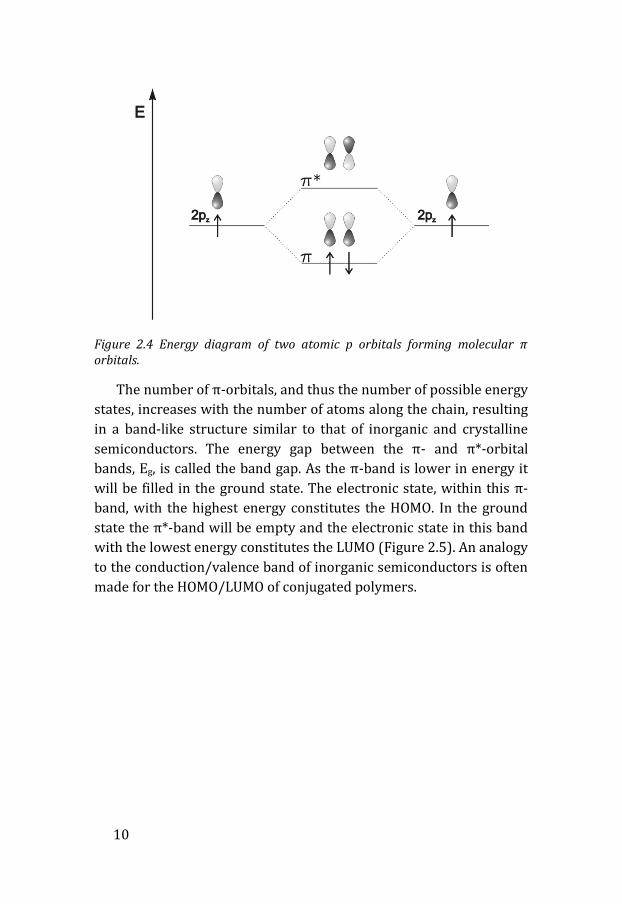
2.1.3 Electronic structure of conjugated polymers In a chain of sp2-hybridized carbon atoms the electrons of the sp2-
orbitals are strongly localized in σ-bonds between the atoms while
the electrons in the orthogonally oriented p-orbitals are free to
overlap with the p-orbitals of the adjacent carbon atoms (Figure 2.4).
If the carbon atoms were equally spaced, along the chain, the
electrons of these overlapping p-orbitals would be de-localized as the
energy states would be equal and thus have the same probability.
This would then lead to a one-dimensional conductor. The total
energy of the molecular chain can however be lowered by alternating
the bond length leading to a, so called, conjugated structure with
alternating double and single bonds. This creates an energy gap
between the filled π-orbitals and the empty π*-orbitals.
10
Figure 2.4 Energy diagram of two atomic p orbitals forming molecular π orbitals.
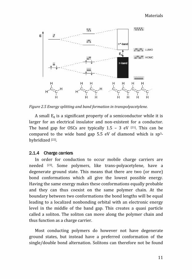
The number of π-orbitals, and thus the number of possible energy
states, increases with the number of atoms along the chain, resulting
in a band-like structure similar to that of inorganic and crystalline
semiconductors. The energy gap between the π- and π*-orbital
bands, Eg, is called the band gap. As the π-band is lower in energy it
will be filled in the ground state. The electronic state, within this π-
band, with the highest energy constitutes the HOMO. In the ground
state the π*-band will be empty and the electronic state in this band
with the lowest energy constitutes the LUMO (Figure 2.5). An analogy
to the conduction/valence band of inorganic semiconductors is often
made for the HOMO/LUMO of conjugated polymers.
Materials
11
Figure 2.5 Energy splitting and band formation in transpolyacetylene.
A small Eg is a significant property of a semiconductor while it is
larger for an electrical insulator and non-existent for a conductor.
The band gap for OSCs are typically 1.5 – 3 eV [21]. This can be
compared to the wide band gap 5.5 eV of diamond which is sp3-
hybridized [22].
2.1.4 Charge carriers In order for conduction to occur mobile charge carriers are
needed [23]. Some polymers, like trans-polyacetylene, have a
degenerate ground state. This means that there are two (or more)
bond conformations which all give the lowest possible energy.
Having the same energy makes these conformations equally probable
and they can thus coexist on the same polymer chain. At the
boundary between two conformations the bond lengths will be equal
leading to a localized nonbonding orbital with an electronic energy
level in the middle of the band gap. This creates a quasi particle
called a soliton. The soliton can move along the polymer chain and
thus function as a charge carrier.
Most conducting polymers do however not have degenerate
ground states, but instead have a preferred conformation of the
single/double bond alternation. Solitons can therefore not be found
12
in these. If a charge is introduced into a conjugated polymer with a
non-degenerate ground state it will be stabilized by a local
rearrangement of the single/double bond alternation around the
point of the charge. This introduces localized states around the
deformation that are called polaron states. It can be energetically
favorable to have two such deformations locally configured and
coupled to each other. Such a localized double-charged state is
referred to as a bipolaron.
The charge carriers can move along a polymer chain as a localized
package, which alternates the bond conformation as it is transported
along the chain. This explains the conduction mechanism that occurs
along the individual polymer chains. To have conduction in a bulk
material the charges also have to cross from one chain to another. In
systems with low order at normal temperature this intermolecular
charge transport is typically dominated by phonon-assisted hopping [24].
2.1.5 Doping
The conductivity of the conjugated polymer bulk is dependent on
mobility and the number of charge carriers. Due to the relatively
large band gap of most conjugated polymers, the number of
thermally induced charge carriers is rather limited, making them in
fact poor conductors in their intrinsic state. To increase the
conductivity more charge carriers must be introduced into the
system. This can be achieved by charge injection, as is the case of
electronic devices such as diodes and field-effect transistors, by
photoexcitation, as in photovoltaics or by doping of the polymer [25].
Doping is the charge-compensation mechanism performed by
introducing a dopant species into the host material, which can
add/donate or remove/accept electrons to, and from, the conjugated
system. If the dopant adds electrons, i.e. reduces the polymer, it is
called n-doping. If it removes electrons from the polymer, i.e. oxidizes
it, it is called p-doping. These redox processes can be induced both
chemically and electrochemically [26-27]. In electrochemical doping a
voltage is applied between the conjugated system and a counter
Materials
13
electrode connected through some solution containing ions, i.e. an
electrolyte. The voltage drives injection of charges into the
conjugated system and ions, of opposite charge, migrates into the
material from the electrolyte to compensate and preserve charge
neutrality [28]. Doping a material can improve the conductivity by
several orders of magnitude [27].
2.2 Polarity of molecules
2.2.1 Electronegativity
The tendency of a chemical element to attract electrons can be
described by a property called electronegativity [19-20]. When two
atoms form a molecular bond, the nature of that bond, and its
included electrons, is decided by the difference in electronegativity of
the two atoms involved. If they have the same electronegativity they
will share these involved electrons equally in a covalent bond. If, on
the other hand, there is a difference in electronegativity the electrons
will be more attracted to one of the atoms and an electric dipole,
along the bond axis, is established. This is called a polar bond. It is
also possible that the difference in electronegativity is so large that
the electrons of the bond will almost completely be located at one of
the atoms alone. That is then called an ionic bond.
2.2.2 Dielectric polarization
When a conductor is placed in an electric field, charges will flow
as a current through the conductor to counter and compensate for
the field. For an electrical insulator charges cannot flow. Instead,
electronic charges involved in bonds of the insulating matter can only
be slightly displaced from their equilibrium position thus minimizing
the field inside the material. This phenomenon is called dielectric
polarization. Depending on the nature of the material the dielectric
polarization can consist of distortion of the electron cloud around the
atoms, the molecular orbitals or, can even lead to a reorientation of
permanent dipoles within the material [29].
14
Reorientation of permanent dipoles is associated with physical
displacement of atoms, which must be accompanied with some sort
of inertia. Thus, the orientation polarization is frequency dependent.
In some cases there is even an apparent energy threshold needed to
overcome before the actual initialization of the dipole reorientation
can occur. These characteristics can give the material so-called
ferroelectric properties and the threshold energy is related to the
amplitude of the internal field of the material that is needed to cause
reorientation of the dipoles. This internal field quantity is called the
coercive field EC [30-31]. Ferroelectric properties can also be achieved
in materials, such as ionic crystals, through ionic polarization [32-33].
The change of orientation of the dipoles in ferroelectric materials
is associated with the electric field. Form this it follows that any
mechanically induced distortion caused to these materials will
typically also induce a change of the electric field inside these
materials. This gives that ferroelectric materials are also both
piezoelectric and pyroelectric [34]. Additionally the internal
orientation of the dipoles will be possible to detect as any change of
them will have a strong effect on the surface charge of the material.
2.3 Electrolytes
An electrolyte is a material system that contains mobile ions thus
making it electrically conductive. Generally speaking, an electrolyte
could be said to consist of salt that dissociates into ions as it is
introduced into a solvent. Positive and negative ions are often
referred to as cations and anions, respectively. Ions are transported
in the electrolyte either by diffusion or migration [19]. Diffusion is the
thermodynamically driven process that leads to spontaneous
dispersion of the ions over time. Migration on the other hand is the
ionic transport caused by the force exerted on the ions in the
presence of an electric field.
Depending on the fraction of the salt that dissociates into ions the
electrolyte can be said to be strong (high fraction) or weak (low
fraction). Different types of electrolytes, that are relevant in organic
Materials
15
electronics, are electrolyte solutions, molten salts, ion gels,
polyelectrolytes and polymer electrolytes. Out of these the most
common are probably electrolyte solutions.
For electrochemical experiments it is sometimes preferred to use
an organic solvent due to their electrochemical stability. However,
for most biological systems the typical electrolyte solvent is water.
Water is in itself a weak electrolyte as it dissociates into hydroxide
and hydronium ions, through autoionization, to a concentration of
about 0.1 µM at neutral conditions (hence pH 7).
2.3.1 Electric double layer
A difference in electric potential between an electrode and an
electrolyte will result in the formation of a so called electric double
layer (EDL) at the electrode/electrolyte interface. In the simplest
model, the EDL can be described as a thin layer of charges on the
electrode surface being compensated by a layer of solvated ions, of
opposite charge, in the electrolyte next to the surface. In reality, a
more complex model is necessary to describe the fundamentals of
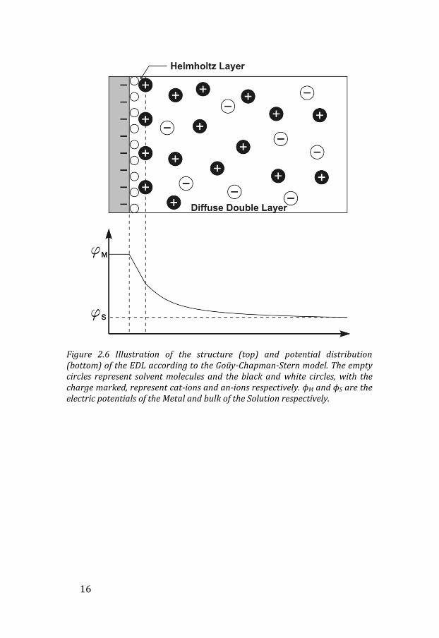
the actual EDL. Commonly the Goüy-Chapman-Stern model (GCS) [35-
36] is used. In the GCS model the charges in the electrolyte are divided
into two layers. Closest to the electrode the ions and solvent
molecules are organized in a rigid planar structure called the
Helmholtz layer. In this layer all the ions are of opposite charge to
those on the electrode. Between the electrode and the Helmholtz
layer the field is constant and the potential drop over this layer is
thus linear. Further away from the electrode the net charge is still of
opposite sign to that of the electrode, but ions of both polarities are
present. This makes the structure more diffuse stretching it out into
the electrolyte. The electrical potential drops exponentially in this
diffuse double layer (Figure 2.6). The total capacitance across an EDL
is typically on the order of tens of µF/cm2 [36-37].
16
Figure 2.6 Illustration of the structure (top) and potential distribution (bottom) of the EDL according to the Goüy-Chapman-Stern model. The empty circles represent solvent molecules and the black and white circles, with the charge marked, represent cat-ions and an-ions respectively. ϕM and ϕS are the electric potentials of the Metal and bulk of the Solution respectively.
17
3. Devices
3.1 Capacitors
Capacitance is a property that describes the ability of a body or
device to store charge. Two electrical conductors separated by some
insulator will constitute a capacitor where the capacitance, C,
between them is defined through the potential, V, between them and
the charge, Q, at each conductor as
18
3.1.1 Electric double layer capacitors
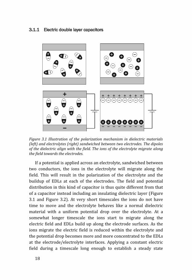
Figure 3.1 Illustration of the polarization mechanism in dielectric materials (left) and electrolytes (right) sandwiched between two electrodes. The dipoles of the dielectric align with the field. The ions of the electrolyte migrate along the field towards the electrodes.
If a potential is applied across an electrolyte, sandwiched between
two conductors, the ions in the electrolyte will migrate along the
field. This will result in the polarization of the electrolyte and the
buildup of EDLs at each of the electrodes. The field and potential
distribution in this kind of capacitor is thus quite different from that
of a capacitor instead including an insulating dielectric layer (Figure
3.1 and Figure 3.2). At very short timescales the ions do not have
time to move and the electrolyte behaves like a normal dielectric
material with a uniform potential drop over the electrolyte. At a
somewhat longer timescale the ions start to migrate along the
electric field and EDLs build up along the electrode surfaces. As the
ions migrate the electric field is reduced within the electrolyte and
the potential drop becomes more and more concentrated to the EDLs
at the electrode/electrolyte interfaces. Applying a constant electric
field during a timescale long enough to establish a steady state

Devices
19
condition, the potential drop will be entirely concentrated to the
EDLs and the electric field will thus be very high at the interfaces and
effectively zero within the bulk of the electrolyte (Figure 3.2) [38].
Figure 3.2 Charge distribution, electric potential (U) and field (E) in an electrolyte capacitor during charging. (a) before voltage is applied, (b) before, (c) during and (d) after charge redistribution.
3.1.2 Super capacitors The EDLs at the electrodes of an electrolyte capacitor can each be
viewed as a very thin parallel plate capacitor. The capacitance of a
parallel plate capacitor is described by the equation
where ε is the permittivity of the material between the capacitor
electrodes, A is the overlapping area of the electrodes and d is the
distance separating the electrodes. The thickness of the EDL
corresponds to d when considering the EDL as a parallel plate
capacitor. Since this is a very small distance the capacitance of the
EDL can get very high. To further increase the capacitance, the area
of the electrode can be increased. By making the electrodes porous it
is possible to achieve very large effective electrode areas in
electrolyte-based capacitors relative to the volume/weight of the
capacitor, thus yielding capacitors with extraordinary high energy
densities. This type of capacitor is called electrolyte supercapacitors.
20
In electric double layer capacitors, such as these electrolyte
supercapacitors, the charge is stored electrostatically [39-40].
3.1.3 Pseudo capacitors
Another way of storing large amounts of charge in electrolyte-
based capacitors is to include electrodes that are electrochemically
active. Charge can then be stored throughout the entire bulk of the
electrodes by reducing or oxidizing the actual electrode material. In
such capacitors, this gives that the entire volume of the electrode
material dictates the capacitance value of the resulting capacitor and
not just the surface area of the electrode. This type of capacitor is
sometimes called a pseudocapacitor as the voltage transients during
charge and discharge are similar to what is found in batteries. In
pseudocapacitors the charge is stored electrochemically [39, 41].
It is also possible to make hybrid capacitors where the charge is
stored electrostatically at one electrode and electrochemically at the
other [42].
3.2 Transistors
Transistors can generally be described as three-terminal devices
in which the resistance, and thus the current, between two of the
terminals can be regulated by addressing the third. This way the
current level between the first two terminals can be modulated and
the transistors can be used in circuits to achieve electronic digital
gates and switches. Transistors can also be used in circuits for
analogue applications to achieve amplifiers. The first transistor, a
type of point contact bipolar junction transistor made from
germanium, was reported in 1947 by Bardeen, Brattain and Shockley
at Bell labs [1], in the US. The transistor could then replace the fragile
and power consuming vacuum tube triodes. Today transistors are
part of almost every piece of electronic equipment.
Devices
21
3.2.1 Thin film transistors
Transistors can also be made from organic materials. Typically a
thin film transistor configuration is then used (TFT) [43]. These types
of transistors have a special configuration where the semiconductor
channel is deposited as a thin film on some form of insulating carrier
substrate. The TFTs are generally speaking field effect transistors
(FET), but in this work we will also discuss yet another type of thin
film transistor, the organic electrochemical transistor (OECT). The
OECT does not operate according to a FET mode of operation but has
many similarities to the FET device with respect to layout and output
characteristics. In fact, the very first organic TFT was an OECT [44]. In
TFTs the channel semiconductor is usually intrinsic (undoped).
3.2.2 Field effect transistors
The field effect transistor was first predicted and patented already
in 1925 by Lilienfeld [45]. It took, however, until 1959 for such a
device to finally be realized [46]. What had then been constructed was
a silicon-based Metal Oxide Semiconductor FET (MOSFET). FETs are
now the most common type of transistor and are included in all kinds
of computers and communication devices. The first FET including an
OSC was reported in 1986 by Tsumura et al [47].
A FET is a three-terminal device where the current between the
source and drain electrodes can be modulated through a voltage
applied to the gate electrode. The source and drain electrodes are
connected by a semiconducting material, which defines the transistor
channel. The gate electrode is separated from the transistor channel
by an electronically insulating material. This insulator is sometimes
referred to as the gate dielectric, but it can also be, e.g. an electrolyte
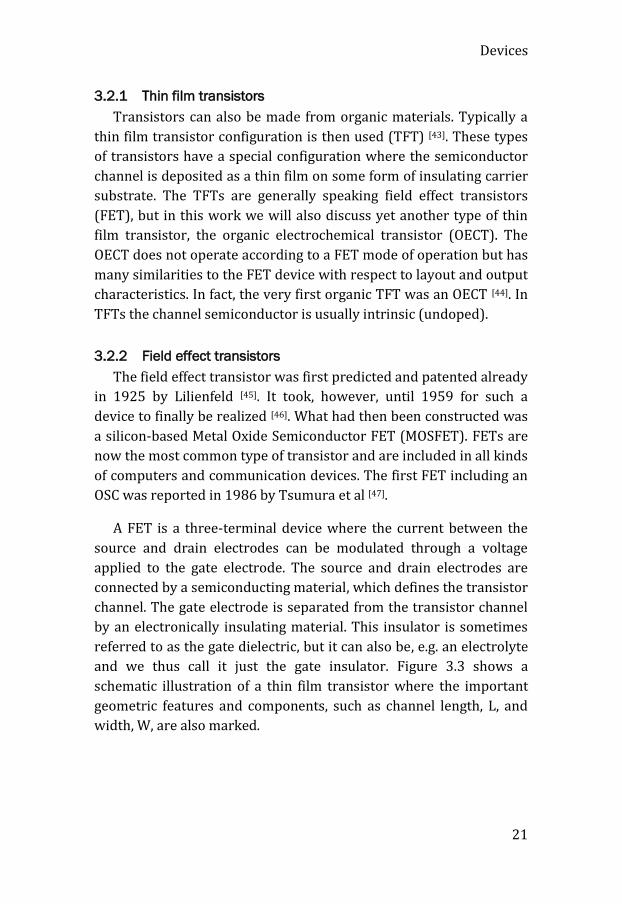
and we thus call it just the gate insulator. Figure 3.3 shows a
schematic illustration of a thin film transistor where the important
geometric features and components, such as channel length, L, and
width, W, are also marked.
22
Figure 3.3 Schematic illustration of an organic thin film transistor with channel length L and width W.
3.2.3 Transistor operation The gate/insulator/channel stack can be viewed as a capacitor.
The properties of this capacitor is important as it predicts the
number of charges present in the channel and thus the number of
charge carriers, which in turn dictates the conductivity and
throughput of the transistor. For capacitors we know that the
capacitance is given by
If the capacitance, Ci, of the insulator is independent of the voltage
applied, we thus get the very simple relation between the charges
induced in the semiconductor and the voltage applied to the gate
The charges in the semiconductor are mostly concentrated to the
semiconductor/insulator interface and an applied voltage creates a,
more or less, two-dimensional, conducting transistor channel,
between the source and drain electrodes, close to this interface [43].
The conductivity of the transistor channel can thus be modulated
through changes in the applied gate voltage.
However, charges can be present along the semiconductor, also
without applying an external voltage, due to e.g. doping of the

Devices
23
semiconductor, trapped charges that exists along the semiconductor
interface and that there exists a difference in work function between
the gate electrode and the semiconductor material. This means that
there might be some level of the applied gate voltage that needs to be
exceeded before the channel becomes conducting [48]. This voltage is
termed the threshold voltage, VT, and the number of mobile charges
as a function of the applied Gate-Source Voltage, VGS, in the channel is
thus given by the equation
If the VGS applied is positive the induced charges within the
channel will be negative and vice versa. A positively charged channel
is referred to as a p-channel and a negatively charged channel as an
n-channel.
In some cases it is possible to use an electrolyte as the gate
insulator. The gate/insulator/channel stack then constitutes an
electric double layer capacitor and the associated capacitance can
thus be very high. As can be seen in the equation above, a high
insulator capacitance means that the number of induced charges in
the channel will be much larger and sensitive to changes in the gate
voltage, making it possible to produce transistors operating at very
low voltages. This kind of transistor is called electrolyte-gated FETs
(EGFET). If the semiconductor material is organic they are commonly
referred to as EGOFETs where the added ‘O’ marks organic.
Assuming that the source electrode is grounded there are two
transistor electrode voltages that can be varied and controlled in an
FET, the Gate-Source Voltage (VGS) and Drain-Source Voltage (VDS).
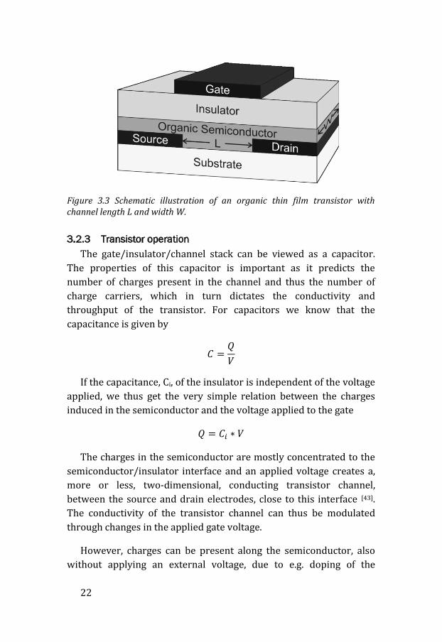
Transistor characteristics curves can be produces by keeping one of
these voltages constant while sweeping the other at the same time
measuring the drain current response. The current at the three
terminals (IG, ID, IS) are defined as being positive while entering into
the transistor and Kirchhoff’s current law tells us that the sum of
them should be zero. Plotting ID against VGS yields the classical
transfer characteristics. By plotting the ID versus VDS the so-called
output characteristics are achieved (see Figure 3.4).
24
The transfer characteristics are usually plotted with ID on a log
scale versus VGS as the current can vary with several orders of
magnitude. Below VT of the transistor the current is dominated by
diffusion instead of drift and there is an exponential relationship
between ID and VGS [6] determined by the insulator capacitance and
the density of trap states, at the interface between the semiconductor
and insulator materials, as well as temperature. Filling of traps is
typically crucial in determining the ID versus VGS evolution. This
subthreshold region is quantified by the subthreshold swing S
At even lower gate voltages there is no longer any noticeable
modulation of the current and the measured current can be
attributed to leakage and charging. The particular voltage point,
below which there is no current modulation, is called the switch-on
voltage (VSO) [49]. At voltages below VSO the transistor is said to be in
the off state.
Figure 3.4 Typical current-voltage characteristics of an organic field effect transistor. (Left) output characteristics with linear and saturation regimes marked out. (Right) Transfer characteristics with on/off current ratio, switch-on voltage (VSO), threshold voltage (VT), subthreshold swing (S) as well as the different regimes marked out.
Devices
25
At voltages greater than VT the behavior of the current response
can be estimated as following the transistor equations derived and
given below.
For the equation presented above which predict the number of
mobile charges within the channel we assume that the source and
drain voltages are both grounded. If a voltage is applied to the drain
electrode there will be a drop of the voltage from drain to source and
the difference in voltage between the gate and the channel, and thus
the number of induced charge carriers, will therefore differ along the
channel. The charge density, at some position x along the channel, is
given by
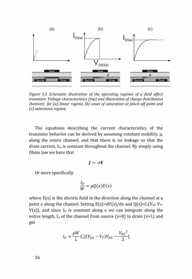
If the Drain-Source Voltage, VDS, is small, so that VDS VGS-VT, the
potential difference between the gate and the channel will more or
less be uniform along the whole channel. Because of this the mobile
charge density, and thus the conductivity, will also be almost uniform
along the whole channel and the Drain current, ID, will increase
linearly with the applied VDS. This is called the linear regime of the
transistor. As VDS approaches VGS-VT the density of mobile charges
will get noticeably lower towards the drain electrode, which also
means that the conductivity reduces close to the drain electrode and
the slope of the ID vs. VDS becomes less and less steep. When VDS = VGS -
VT the mobile charge density at the edge of the drain electrode will
theoretically be zero. The point in the channel where the potential is
equal to VGS-VT is referred to as the pinch of point (P). Increasing VDS
even further will then move P further away from the drain electrode,
towards the source electrode and thus increases the fraction of the
channel that has a low conductivity. This gives that ID will saturate,
i.e. ID more or less stops increasing with an increase of VDS and this is
thus called the saturation regime of the transistor (Figure 3.5).
26
Figure 3.5 Schematic illustration of the operating regimes of a field effect transistor. Voltage characteristics (top) and illustration of charge distribution (bottom) for (a) linear regime, (b) onset of saturation at pinch-off point and (c) saturation regime.
The equations describing the current characteristics of the
transistor behavior can be derived by assuming constant mobility, µ,
along the entire channel, and that there is no leakage so that the
drain current, ID, is constant throughout the channel. By simply using
Ohms law we have that
Or more specifically
where E(x) is the electric field in the direction along the channel at a
point x along the channel. Setting E(x)=dV(x)/dx and Q(x)=Ci(VGS-VT-
V(x)), and since ID is constant along x we can integrate along the
entire length, L, of the channel from source (x=0) to drain (x=L) and
get
Devices
27
In the linear regime (VDS VGS-VT) this equation can be simplified
to
The saturation current can be calculated by simply setting VDS =
VGS-VT
Considering the transistor characteristics and fitting the data of
the transfer characteristics to the transistor equations makes it
possible for us to extract transistor parameters such as the mobility
and the threshold voltage.
Another transistor characteristic, which is often considered one of
the most crucial and representative, is the transconductance gm. It
describes how the output current ID is modulated by the input
voltage VGS, such that gm = ∂ID/∂VGS at a constant VDS [6]. The
transconductance is thus different in the linear and saturation
regimes
3.2.4 Electrochemical transistors
In EGOFETs the EDL at the electrolyte/semiconductor layer
interface is well defined. This means that the ions in the electrolyte
and the induced electronic charges in the semiconductor are
28
separated and constrained to their respective medium along the
interface [37].
It is sometimes possible for ions from the solution to breach the
interface and then migrate into the bulk of the organic
semiconductor material [50]. This gives a less well, or even ill-, defined
EDL and the mechanisms that modulate the transistor current is no
longer constrained to just the surface of the semiconductor, but also
occur throughout the entire bulk. The introduction of charged species
into the semiconductor material can be viewed as doping of the
entire bulk and, as the process is driven by an electrical potential,
transistors modulated in this manner are called (organic)
electrochemical transistors (OECT). We can speculate over what
mechanism is responsible for the transistor modulation for different
cases and kinds of OECTs. It could in some cases be due to
electrochemical redox reactions of the polymer channel in which
charge transfer actually takes place between the introduced ions and
the OSC. It could however also be speculated that the OECT mode of
operation is due to ion exchange and charge compensation. The latter
mechanisms would then define a transistor that operates according
to principles more similar in nature to the mechanism of modulation
taking place in EGOFETs. Regardless of which mechanism that
governs the operation in the OECTs, the drain current level in the
transistors will scale with the thickness of the semiconductor layer as
the gate potential modulates the conductivity of the entire bulk.
Furthermore, the OECTs modulation is generally slower as it not only
depends on the time it takes to form the EDL, which depends on the
diffusion rate in the electrolyte, but also the diffusion or migration
rate of the entering ions inside the OSC. As ions propagate further
and further into or out from the semiconductor film, more or less of
the semiconductor material will take part in the formation of the
transistor channel, and conduction of charges, through the transistor
and with this propagation an evolution of the ID will follow. The fact
that the charges need to be moved in and out of the semiconductor
thus gives some memory/hysteresis effects that typically appear at
high frequency biasing.
Devices
29
3.2.5 Electrolyte gated thin film transistor sensors
The channel conductivity in a FET is highly dependent on the
induced charge carriers established along the channel. From this, one
can achieve an amplified response to any voltage change recorded at
the gate terminal or to modifications of the charge transport
characteristics occurring along the channel itself. Such an event could
e.g. be an actual change in the gate potential, but it is possible to also
conceive of other origins for such a change. For this reason, TFTs are
considered, and heavily explored, as an attractive component in
different sensors as they can provide an amplified signal, and thus an
increased sensitivity, for a variety of sensors. Several different
sensors utilizing a TFT to amplify the sensor signal have been
proposed.
Chemical and biochemical reactions that take place on the surface
or within the semiconductor bulk can potentially be transduced by a
TFT if these reactions are accompanied with a change in the electric
charge carrier density. This will then impact the conductivity and the
drain current of the channel. Examples of such reactions could be the
binding or release of charged species on or adjacent to the
semiconductor channel [51]. This type of sensor could be made as a
simple two-terminal chemresistor device where the bound charges
would mimic the role of an applied gate voltage in the corresponding
three-terminal transistor. The concentration of the bound charges
could then be thought of as corresponding to the amplitude of said
applied gate voltage. A reference electrode is however often added in
the electrolyte as this gives a much better defined system with more
reliable sensing. Adding an actual gate terminal to such chemresistor
sensors could make it possible to control the sensitivity of the sensor
as biasing the gate voltage will have impact on which part of the
transfer characteristics that will correspond to the baseline of the
sensor [52]. It is possible that this type of TFT sensor could function
for both OFETs and OECTs. For OECTs, the whole bulk of the
semiconductor takes part in the formation of the transistor channel.
This gives that the majority of the possible transistor charge carriers
could be completely unaffected by a changes occurring only on the
surface. The charges, taking part in the sensing event, thus need to
30
also migrate throughout the entire semiconductor bulk or the
sensitivity would be significantly reduced.
If the TFT semiconductor layer is thin enough a sensing event
could also take place on the side of the semiconductor layer that is
not in contact with the gate dielectric. A prerequisite for this is also
that the change in charge, induced by the sensing event, induces a
large enough field to significantly affect the entire semiconductor
film.
TFTs can be operated using an electrolyte as the gate insulator.
This provides us with an opportunity to introduce the analyte,
through the electrolyte, in between the gate and the channel. This
then offers an even greater opportunity to achieve sensors with very
high sensitivity. Further, in EGOFET sensors the introduction of
charges via sensor reactions in direct proximity of the transistor
channel would naturally provide an opportunity for high sensitivity.
A sensing event involving immobilization of charge could also
possibly take place at the gate electrode [53] (see Figure 3.6d). The
EDLs, at the channel and gate, can be viewed as two separate
capacitors connected in series and we know from Kirchhoff’s laws
that the charge stored in both these capacitors then must be the
same. A change in charge at the gate should then thus effectively also
mean an equivalent change in the charge at the channel. Not only
direct changes or switching of the charge in the gate-electrolyte-
semiconductor configuration could possibly be monitored and
sensed by an EGOFET sensor. If for instance uncharged species bind
to the surface of the channel it could distort the EDL at the channel in
various aspects, such as effectively increasing the distance that
separates the charges of the semiconductor and the electrolyte in the
EDL [54]. This then lowers the actual capacitance value of the EDL at
this interface and thus affects the transistor current. This sensing
approach would most likely be more effective for EGOFETs than for
OECTs as the current modulation in OECTs is dependent on charges
penetrating into the semiconductor bulk. The static drain current
level of an OECT is expected to be relatively more insensitive to such
in-binding occurring along the surface of the semiconductor. One
Devices
31
could however imagine that the analyte (if small enough), could also
penetrate into the bulk of the semiconductor material and thus
change the possible concentration of the dopant charges that predicts
the drain current level. Another sensing approach for the OECTs is if
the bound analyte blocks the doping ions from migrating in or out of
the semiconductor. This would then suppress the possibility to
modulate the drain current of the transistor. This approach would
then probably have the drawback of only be able to give a binary, e.g.
detection, response to some threshold value of the analyte and would
therefore not be suitable for quantitative analysis [55].
Immobilizing charges on the channel or the gate electrode should
ideally be detectable as a shift in the threshold voltage. Disturbing
the EDL at the channel (without immobilizing charge) should ideally
only change the effective Ci which would be seen as change in the
slope of the transfer curve [54].
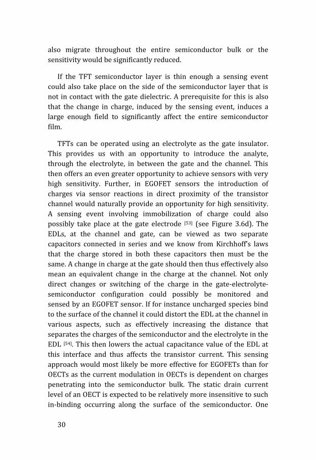
Figure 3.6 Different architectural designs for thin film transistor sensors. The dotted line in each image marks the location of the sensing event.
32
In Figure 3.6 an effort is made to illustrate the different
approaches of using OTFTs in sensor devices. In Figure 3.6a the
transistor is not gated through the electrolyte, including the analyte,
and thus the electrolyte is not an active component of the transistor
architecture [56-57]. Analytes present in the electrolyte that attaches to
the OSC can however still affect the density of charges and traps in
the OSC and the gate electrode can then be used to make the
transistor operate at optimal sensitivity and amplification. In Figure
3.6b there is a dielectric layer introduced between the OSC and the
electrolyte. Analytes attaching to, or reacting with, this dielectric
material may then change the voltage drop over the dielectric layer
which in turn can be observed as a change in the transistor behavior.
The transducer mechanism can in this case originate from the effect
of charges entering into the dielectric, equivalent to mode of
operation present in Ion Selective FETs (ISFET), or simple
displacement of the charges established along the
dielectric/electrolyte interface [54, 58]. Excluding the dielectric layer in
this type of device yields the architecture given in Figure 3.6c. Here,
the OSC is in direct contact with the electrolyte, thus typically
providing relatively higher sensitivity. However such a sensor
approach is also associated with the risk that ionic species from the
electrolyte can penetrate or directly react with the OSC. This gives
that the measured sensor effect on the conductivity of the transistor
channel is no longer just a result of a field effect [59-61], but can instead
be attributed to electrochemical doping, the introduction of traps or
rearrangements of the polymer chains. Further, the sensing event
can also be introduced at the gate electrode, see Figure 3.6d, as this
may change the charge or the effective work function (potential) of
the gate, which in turn would influence the charging of the transistor
channel [62]. There are also successful approaches where the sensing
event has been entirely separated from the transistor channel and
instead utilizes charging of a floating gate [63]. In such an approach,
the sensor reaction is chemically completely de-coupled from the
transistor channel-insulator-gate configuration.
Devices
33
3.3 Ferroelectric surfaces
Since the net surface charge, defined by the orientation of the
included dipoles, of ferroelectric thin films are fixed on the surface,
and thus non-Faradaic, they may not spontaneously be able to
rearrange if the film is placed in contact with an electrolyte. Instead
the charges in the electrolyte will have to adapt to the film and the
EDLs of such systems can thus be said to be more well defined, as
compared to, e.g. the EDL along a metal surface [64].
A ferroelectric thin film can be placed in between two electrodes
to define a two-electrode switch device. By applying a voltage
between the conductors, so that the electric field in the ferroelectric
becomes larger than the coercive field (EC) the dipoles will switch
and align [65-66]. An electrolyte layer can be placed between the
ferroelectric thin film and one of the electrodes. In this case the
potential distribution will be somewhat different as compared to the
former electrode-ferroelectric-electrode case. As the voltage, applied
to the two electrodes, is increased and finally expresses an electric
field inside the ferroelectric layer larger than EC, ferroelectric
polarization will still occur and dipoles will thus align with the field.
Once removing the applied potential the induced polarization of the
ferroelectric dipoles will remain, meaning that the EDL at the
ferroelectric surface will again be stabilized, without an externally
applied voltage, but of opposite polarization as before.
Surfaces with different surface energy or charge can have major
impact on e.g. chemical and biological species, such as self-organized
layers, cells and tissues, in an aqueous solution. It is possible to
create and redefine regions of different polarity, and thus different
surface energy and charge, on the surface of a ferroelectric thin film
placed in an electrolyte [64]. This could provide an opportunity for
spatiotemporal and active control over the adhesion, growth,
organization and release of chemical and biological systems while
interacting with the ferroelectric surface as it undergoes switching.
In addition, the regions of different polarity will be stable without
having to connect the system to an electrical circuit with any external
voltage source, which means that no power is consumed simply to

34
preserve a polarization state. Also, as the electroactive surface is
switching, the ferroelectric layer does not cause any charge transfer
with the aqueous solution, thus limiting undesired electrochemical
side reactions.
35
4. Experimental Methods
4.1 Fabrication
All of the devices presented in this manuscript are based on a
substrate of some form with one or more thin layers of material.
Some of these layers comprise an “active” component of the device,
while others comprise passive or encapsulating materials. In
addition, each of the device’s layers generally involve some form of
macroscopic or microscopic patterning to define individual features.
The following sections describe the various techniques used to
fabricate the devices in Papers I-V.
4.1.1 Thermal evaporation
Thermal evaporation is one form of physical vapor deposition, in
which a material is evaporated from a source in vacuum and
condensed onto a target substrate forming a thin film. Keeping the
source and target in vacuum both creates a free path for the
evaporated particles to travel directly from the source to the target
(Figure 4.1), and reduces the required evaporation or sublimation
temperature. Placing a quartz crystal microbalance (QCM) in the
evaporation chamber, close to the target, makes it possible to record
deposition in real time, and precisely control the evaporation rate

36
and resulting film thickness. It is possible to transfer patterns onto
the target substrate by using stencils, sometimes referred to as
shadow masks.
Figure 4.1 Deposition of a thin film through thermal evaporation. The deposition material is placed in the source and is evaporated through heating of the source. A shadow mask can be placed in between the source and the target substrate as to create patterns in the resulting film.
4.1.2 Photolithography One versatile method for creating highly precise patterning on a
substrate is through photolithography. The surface to be patterned is
first covered in a photosensitive material known as a photoresist. A
mask with the desired pattern is placed over the substrate so that
only some parts can be exposed to light. Exposing the photoresist to a
light source (typically UV) triggers a chemical reaction (generally
either a cross-linking, strengthening reaction, or a degrading
reaction) in the resist, only in the areas exposed through the mask
pattern. The exposed substrate can then be developed, similar to
developing an exposed photograph, using a chemical developer
specific to the photoresist used [67]. If the exposed areas of the
photoresist become more soluble in the developer solution, it is
called a positive photoresist. If the exposed areas become less soluble
it is called a negative photoresist. After processing with the
developer solution, some regions will still be covered with
photoresist, while other will not. The exposed areas can thus be
processed, e.g. through wet or dry etching (i.e. removing material by
exposing it to some reactant gas, plasma or solution), while the
Experimental methods
37
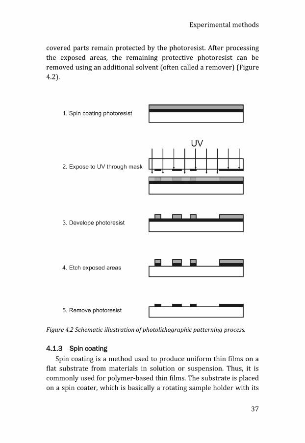
covered parts remain protected by the photoresist. After processing
the exposed areas, the remaining protective photoresist can be
removed using an additional solvent (often called a remover) (Figure
4.2).
Figure 4.2 Schematic illustration of photolithographic patterning process.
4.1.3 Spin coating Spin coating is a method used to produce uniform thin films on a
flat substrate from materials in solution or suspension. Thus, it is
commonly used for polymer-based thin films. The substrate is placed
on a spin coater, which is basically a rotating sample holder with its
38
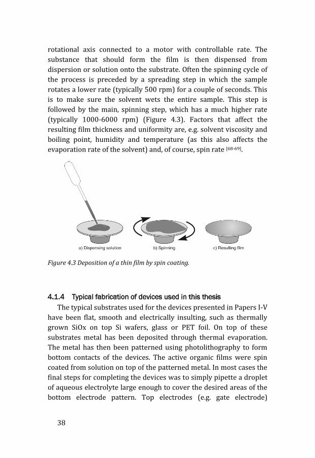
rotational axis connected to a motor with controllable rate. The
substance that should form the film is then dispensed from
dispersion or solution onto the substrate. Often the spinning cycle of
the process is preceded by a spreading step in which the sample
rotates a lower rate (typically 500 rpm) for a couple of seconds. This
is to make sure the solvent wets the entire sample. This step is
followed by the main, spinning step, which has a much higher rate
(typically 1000-6000 rpm) (Figure 4.3). Factors that affect the
resulting film thickness and uniformity are, e.g. solvent viscosity and
boiling point, humidity and temperature (as this also affects the
evaporation rate of the solvent) and, of course, spin rate [68-69].
Figure 4.3 Deposition of a thin film by spin coating.
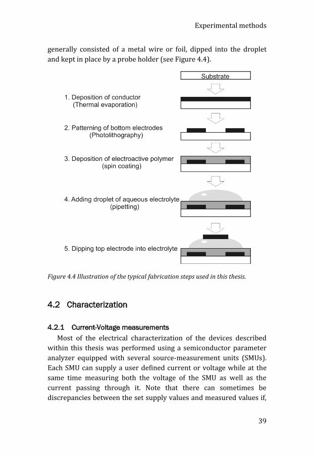
4.1.4 Typical fabrication of devices used in this thesis The typical substrates used for the devices presented in Papers I-V
have been flat, smooth and electrically insulting, such as thermally
grown SiOx on top Si wafers, glass or PET foil. On top of these
substrates metal has been deposited through thermal evaporation.
The metal has then been patterned using photolithography to form
bottom contacts of the devices. The active organic films were spin
coated from solution on top of the patterned metal. In most cases the
final steps for completing the devices was to simply pipette a droplet
of aqueous electrolyte large enough to cover the desired areas of the
bottom electrode pattern. Top electrodes (e.g. gate electrode)
Experimental methods
39
generally consisted of a metal wire or foil, dipped into the droplet
and kept in place by a probe holder (see Figure 4.4).
Figure 4.4 Illustration of the typical fabrication steps used in this thesis.
4.2 Characterization
4.2.1 Current-Voltage measurements Most of the electrical characterization of the devices described
within this thesis was performed using a semiconductor parameter
analyzer equipped with several source-measurement units (SMUs).
Each SMU can supply a user defined current or voltage while at the
same time measuring both the voltage of the SMU as well as the
current passing through it. Note that there can sometimes be
discrepancies between the set supply values and measured values if,
40
e.g. the power supply exceeds the limits of the equipment. Current-
Voltage (I-V) measurements are a fundamental tool for
characterizing and elucidating device dynamics. It is used to
characterize all kinds of electrical devices ranging from transistors to
solar cells and memory devices.
4.2.2 Impedance spectroscopy
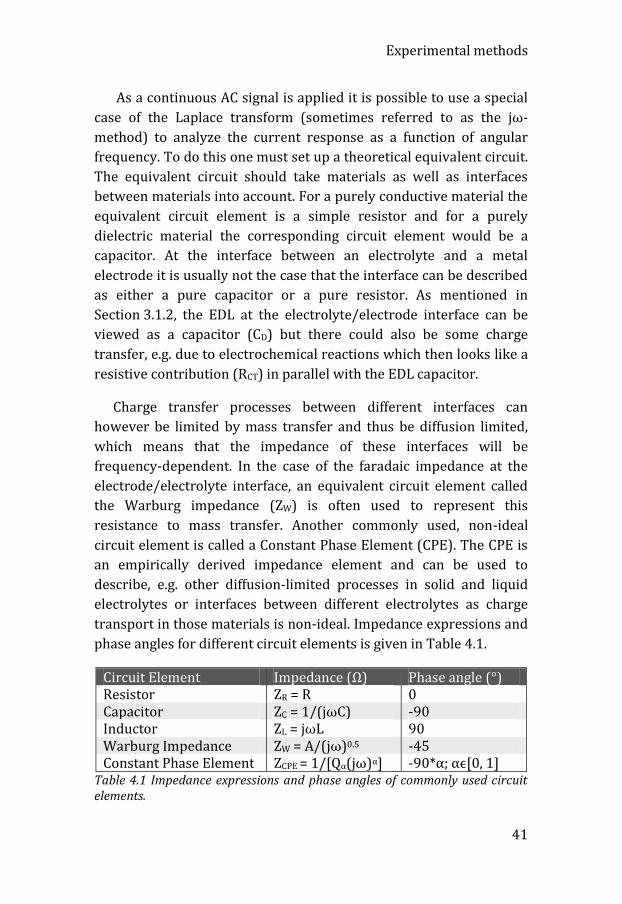
Impedance spectroscopy is a technique that can be used to
characterize a material’s or device’s various electrical properties,
such as transfer resistance, ohmic resistance and double layer
capacitance of an electrolyte [36, 38]. The materials or compound of
materials to be investigated is placed between two electrodes thus
creating some kind of capacitor-like structure. A sinusoidal voltage
signal of known amplitude, frequency and offset is applied between
the electrodes and the current response is recorded. From this the
complex impedance for the entire sample at the specified frequency
can be calculated. By scanning a range of frequencies it is possible to
elucidate various properties of the sample being investigated. The
complex impedance as a function of frequency f, or more commonly
angular frequency ω=2πf is given by,
where U* and I* are the complex voltage and current respectively.
The complex impedance can also be represented by its real and
imaginary components as,
Due to the complex impedance, there can sometimes be a shift in
phase between the voltage and current signals. This shift is defined
as the phase angle,
Experimental methods
41
As a continuous AC signal is applied it is possible to use a special
case of the Laplace transform (sometimes referred to as the jω-
method) to analyze the current response as a function of angular
frequency. To do this one must set up a theoretical equivalent circuit.
The equivalent circuit should take materials as well as interfaces
between materials into account. For a purely conductive material the
equivalent circuit element is a simple resistor and for a purely
dielectric material the corresponding circuit element would be a
capacitor. At the interface between an electrolyte and a metal
electrode it is usually not the case that the interface can be described
as either a pure capacitor or a pure resistor. As mentioned in
Section 3.1.2, the EDL at the electrolyte/electrode interface can be
viewed as a capacitor (CD) but there could also be some charge
transfer, e.g. due to electrochemical reactions which then looks like a
resistive contribution (RCT) in parallel with the EDL capacitor.
Charge transfer processes between different interfaces can
however be limited by mass transfer and thus be diffusion limited,
which means that the impedance of these interfaces will be
frequency-dependent. In the case of the faradaic impedance at the
electrode/electrolyte interface, an equivalent circuit element called
the Warburg impedance (ZW) is often used to represent this
resistance to mass transfer. Another commonly used, non-ideal
circuit element is called a Constant Phase Element (CPE). The CPE is
an empirically derived impedance element and can be used to
describe, e.g. other diffusion-limited processes in solid and liquid
electrolytes or interfaces between different electrolytes as charge
transport in those materials is non-ideal. Impedance expressions and
phase angles for different circuit elements is given in Table 4.1.
Circuit Element Impedance (Ω) Phase angle (°) Resistor ZR = R 0 Capacitor ZC = 1/(jωC) -90 Inductor ZL = jωL 90 Warburg Impedance ZW = A/(jω)0.5 -45 Constant Phase Element ZCPE = 1/[Qα(jω)α] -90*α; αϵ[0, 1]
Table 4.1 Impedance expressions and phase angles of commonly used circuit elements.
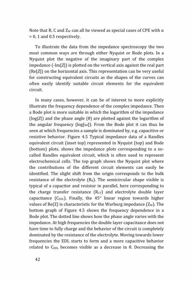
42
Note that R, C and ZW can all be viewed as special cases of CPE with α
= 0, 1 and 0.5 respectively.
To illustrate the data from the impedance spectroscopy the two
most common ways are through either Nyquist or Bode plots. In a
Nyquist plot the negative of the imaginary part of the complex
impedance (-Im[Z]) is plotted on the vertical axis against the real part
(Re[Z]) on the horizontal axis. This representation can be very useful
for constructing equivalent circuits as the shapes of the curves can
often easily identify suitable circuit elements for the equivalent
circuit.
In many cases, however, it can be of interest to more explicitly
illustrate the frequency dependence of the complex impedance. Then
a Bode plot is more suitable in which the logarithm of the impedance
(log|Z|) and the phase angle (θ) are plotted against the logarithm of
the angular frequency (log[ω]). From the Bode plot it can thus be
seen at which frequencies a sample is dominated by, e.g. capacitive or
resistive behavior. Figure 4.5 Typical impedance data of a Randles
equivalent circuit (inset top) represented in Nyquist (top) and Bode
(bottom) plots. shows the impedance plots corresponding to a so-
called Randles equivalent circuit, which is often used to represent
electrochemical cells. The top graph shows the Nyquist plot where
the contributions of the different circuit elements can easily be
identified. The slight shift from the origin corresponds to the bulk
resistance of the electrolyte (RE). The semicircular shape visible is
typical of a capacitor and resistor in parallel, here corresponding to
the charge transfer resistance (RCT) and electrolyte double layer
capacitance (CEDL). Finally, the 45° linear region towards higher
values of Re(Z) is characteristic for the Warburg impedance (ZW). The
bottom graph of Figure 4.5 shows the frequency dependence in a
Bode plot. The dotted line shows how the phase angle varies with the
impedance. At high frequencies the double layer capacitance does not
have time to fully charge and the behavior of the circuit is completely
dominated by the resistance of the electrolyte. Moving towards lower
frequencies the EDL starts to form and a more capacitive behavior
related to CEDL becomes visible as a decrease in θ. Decreasing the
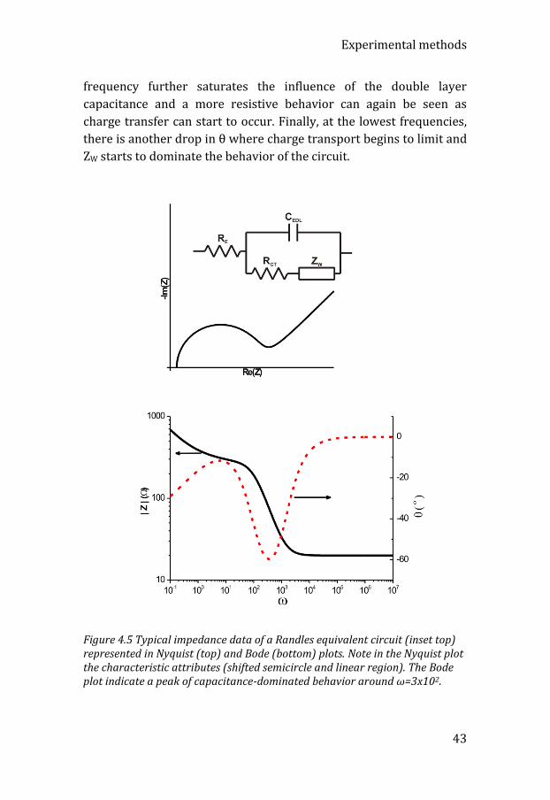
Experimental methods
43
frequency further saturates the influence of the double layer
capacitance and a more resistive behavior can again be seen as
charge transfer can start to occur. Finally, at the lowest frequencies,
there is another drop in θ where charge transport begins to limit and
ZW starts to dominate the behavior of the circuit.
Figure 4.5 Typical impedance data of a Randles equivalent circuit (inset top) represented in Nyquist (top) and Bode (bottom) plots. Note in the Nyquist plot the characteristic attributes (shifted semicircle and linear region). The Bode plot indicate a peak of capacitance-dominated behavior around ω=3x10².

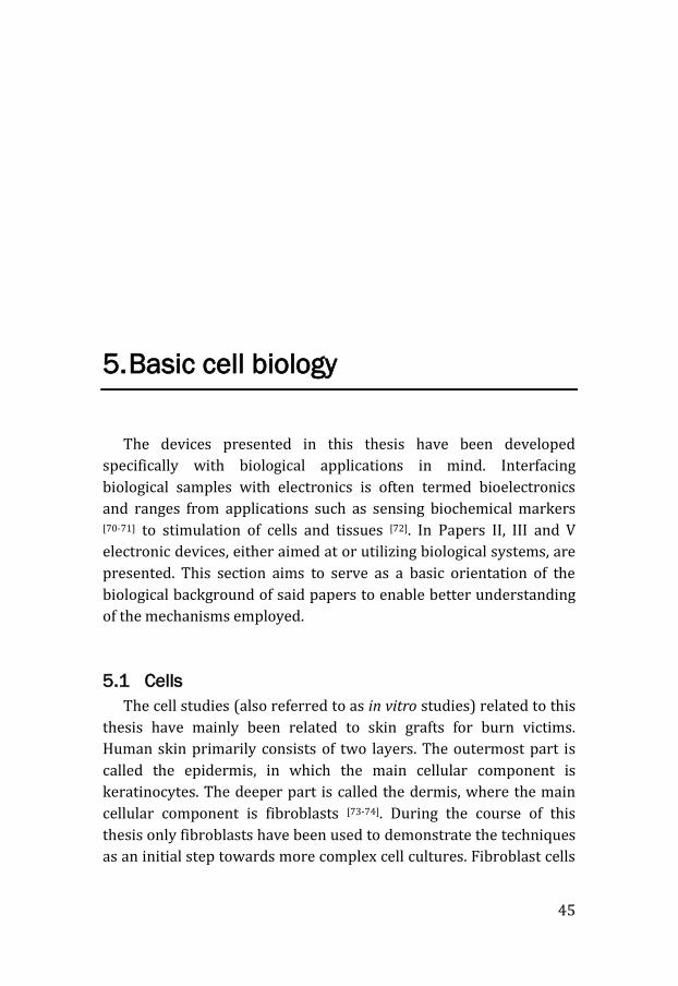
45
5. Basic cell biology
The devices presented in this thesis have been developed
specifically with biological applications in mind. Interfacing
biological samples with electronics is often termed bioelectronics
and ranges from applications such as sensing biochemical markers [70-71] to stimulation of cells and tissues [72]. In Papers II, III and V
electronic devices, either aimed at or utilizing biological systems, are
presented. This section aims to serve as a basic orientation of the
biological background of said papers to enable better understanding
of the mechanisms employed.
5.1 Cells
The cell studies (also referred to as in vitro studies) related to this
thesis have mainly been related to skin grafts for burn victims.
Human skin primarily consists of two layers. The outermost part is
called the epidermis, in which the main cellular component is
keratinocytes. The deeper part is called the dermis, where the main
cellular component is fibroblasts [73-74]. During the course of this
thesis only fibroblasts have been used to demonstrate the techniques
as an initial step towards more complex cell cultures. Fibroblast cells
46
are generally present in connective tissues, where they are often the
most numerous cells. Their primary role is to produce the fibers and
ground substance of the extracellular matrix [74]. Fibroblasts thus also
play an important role in wound healing and reformation of tissues [73].
5.2 Phospholipids and the cell membrane The outer surface of cells consists of a cell membrane. This
membrane separates the inside of the cell from its external
environment. The membrane regulates transportation of substances
in and out of the cells and also contains means for cells to
communicate with their environment and other cells [74].
Figure 5.1 Schematic representation of a phospholipid (left) with the polar head and fatty tails and how they can organize into double layers in solution (right).
The cell membrane is composed primarily of phospholipids;
molecules with a polar, hydrophilic phosphate “head” and one or
more non-polar, hydrophobic fatty acid “tails” (Figure 5.1). This
makes them amphiphilic, and in aqueous environments they thus
self-organize tail-to-tail into a double layer, forming the main
structure of the cell membrane [74]. Because of the fatty core of the
phospholipid bilayer, it is impermeable to ions and large polar
Basic cell biology
47
molecules, while at the same time permeable to water and non-polar
molecules.
5.3 Membrane proteins
The cell membrane also contains glycoproteins that can either be
peripheral, located on one side (inside/outside) of the membrane, or
integral proteins, that extend into or through the lipid bilayer.
Membrane proteins, together with glycolipids, play a vital role in
intercell communication. Indeed, the majority of a cell’s interaction
with its environment is mediated through its membrane proteins, e.g.
transporting specific ions or molecules through the membrane, or as
receptors that can recognize and bind to specific molecules [74]. In
some cases, the membrane proteins can be seen as cell identity
markers playing an important part in, for example, tissue formation
or immune response, where cells need to identify and communicate
with their adjacent cells and environment.
5.4 Extracellular matrix
The extracellular matrix (ECM) of connective tissues comprises
some ground substance (water and large organic molecules)
combined with protein fibers. The ground substance can be in fluid,
gel or solid state depending on the tissue. The ECM provides a
structural framework for the tissue’s cells and provides a medium for
transportation of substances between the blood and cells. The
protein fibers of the ECM thus support and strengthen the tissue and
provide anchor points for tissue growth [74-75].
The tripeptide sequence arginine-glysine-aspartic acid (“RGD”, in
single-letter amino acid code) has been shown to bind to specific
receptor proteins in the cell membrane [75]. As the RGD sequence is
present on ECM proteins such as fibronectin and fibrinogen, the RGD
sites are considered to be primary cell anchoring (binding) points.
48
5.5 Binding proteins/mechanisms
Because there are certain amino acids sequences of that are
required for effective cell anchoring/binding – like the RGD sequence
mentioned above – protein conformation, and thus binding-sequence
exposure, becomes very important. When a protein adheres to a
surface it can change conformation depending on properties such as
surface chemistry, energy or charge, which in turn affects the ability
of cells to bind to the proteins on the surface [75]. The surface
properties may also affect the affinity of the proteins themselves,
which then in turn also affects how strongly cells are attached to the
surface through binding to these proteins [75]. It is these surface
effects that are exploited in Paper V.
5.6 Biorecognition events
Since proteins can act as ID-tags for specific cell types or
conditions, many biosensors utilize protein interaction, such as
binding and enzymatic reactions, to achieve a high level of specificity.
One method that has been very successful throughout the years is
using the strong affinity between the enzyme biotin and the protein
avidin, discovered in the 1940s [76], and later also to other proteins
with similar features such as streptavidin [77]. Through the process of
biotinylation, biotin can be attached to different molecules which
then can be detected, or be used to detect, through their high affinity
to biotin binding proteins, such as avidin or streptavidin [78]. For
detection in sensor applications the biotin could e.g. be attached to a
fluorescent probe or, as in Paper II, an organic semiconductor.
5.7 Cell detachment
Cells cultured in vitro must usually at some point be detached
from their substrate for, e.g. analysis, re-seeding or implantation.
There are several strategies applied to achieve this detachment.
Perhaps the most widely used method today is a treatment with the
enzyme trypsin, which cleaves the membrane proteins which bind
the cells to the surface [79]. While this technique can be highly
Basic cell biology
49
effective at detachment, enzymatic treatment of the membrane
proteins can affect the viability of the cells and their ability to bind to
subsequent surfaces or tissues [80-81]. Detachment strategies that
target the substrate itself, rather than the biochemistry of the cells,
have thus been proposed.
Electroactive release of the entire substrate surface is one
strategy. In this method, cells are cultured on an intermediate surface
which can be electronically released from the main substrate. The
cells are thus released along with the intermediate layer, and can
subsequently be collected and reseeded [82-85]. Such electroactive
strategies also have the potential for spatial as well as temporal
control of the release of cells from the substrate surface, as individual
release areas or “pixels” could be defined.
Other methods of cell release have also been proposed or
demonstrated. For example, changing the surface energy of the
substrate via thermally-induced effects has been demonstrated [86-88],
and in Paper V we demonstrated an entirely new electroactive cell
release method using ferroelectric films.

51
6. Conclusions and future outlook
The focus of this thesis has been on the challenges and
opportunities faced when placing organic electronics in aqueous
environments and even using these environments as active
components of the devices. We have explored how the polarization of
an electrolyte in contact, and circuit, with various electroactive
polymer thin films can be exploited to modulate the devices. We have
also demonstrated how changes in the EDL, at the interface with the
polymer thin films, can be used both for sensing and modulating
events at the interface.
Papers I, II and III all touch on the subject of when and how it is
possible to make use of the high capacitance of the EDL, and its
sensitivity to local changes, in transistor-based sensors. Transistor
modulation via EDLs can be complicated – and even diminished – by
electrochemical doping of the semiconductor, in competition with the
field-effect of the EDL. This could in turn thus also diminish the
sensor signal. However, if one can make certain that the dominant
modulation mechanism is through field effect, EDL-based systems
can be utilized. This restriction to field-effect can be achieved by
suppressing the availability of the semiconductor bulk to the ions of
the electrolyte. Two strategies are presented within this thesis, the
52
first being to decrease the ion mobility in the semiconductor by using
a co-polymer with a sufficiently large hydrophobic part (Paper I and
II). The second strategy involves adding another layer on top of the
semiconductor, thus slightly separating it from the electrolyte (Paper
III). In the case presented in Paper III it can be seen that there is
some form of charge transfer over one of the interfaces as there must
be a CPE included in the equivalent circuit model to properly fit the
impedance data. In both of the cases it becomes apparent from the
impedance data that the frequency of the applied signal has an effect
on the behavior of the devices. This should most likely translate into
an effective time limit for applying a gate voltage before risking ion
penetration into the semiconductor bulk. Taking these design
parameters into account should vastly expand the number of
possible semiconductor materials and device architectures that can
be utilized for aqueous in situ transistor-based sensing applications.
In Papers IV and V the focus shifted from how the electrolyte
affects the electroactive polymer to how the electroactive polymer
can affect the electrolyte, specifically the EDL. We demonstrate how
the EDL can be formed at the surface of a ferroelectric film, and how
the surface charge of the ferroelectric material affects the total
charge of the EDL. The surface change on the ferroelectric material
can thus affect the resulting voltage drop over the EDL. Although the
stabilization of the EDL by ferroelectric surfaces has been
investigated before, the specific voltage induced over the EDL has not
previously been elucidated. It turns out that the (easily measured)
overall device voltage is highly sensitive to changes in the properties
of the EDL, indicating that we may have found a new means of
intimately probing the EDL and events taking place therein. This not
only opens up possibilities of investigating the EDL itself but also
shows promise for new types of sensors with a direct voltage
readout. Such sensors could have extremely low power consumption
as there does not need to be any input power once the ferroelectric
thin film has been polarized.
Well-defined surface charge has also been suggested as a useful
tool for controlling where biological and chemical events can take
Conclusions and future outlook
53
place on a patterned ferroelectric surface. We have shown that it is
possible to change the polarization of a ferroelectric polymer film by
applying a voltage through an electrolyte. This aqueous modulation
of the polarization provides the opportunity to continuously redefine
surface charge patterns and thus control where said biological or
chemical events take place. To demonstrate this ability, we grew cells
on ferroelectric polymer thin films and were able to trigger their
release from the surface by changing the direction of the ferroelectric
polarization in situ. The cells used in our experiments were one type
of skin cells. Tissues are generally composed of several types of cells,
which means that there is still much to explore. Different cell types
may react differently to the different surface energies, meaning that
the technique might be possible to use for organizing or sorting cells
in a culture. Still, ferroelectric cell release represents a promising
alternative to contemporary chemical cell release techniques,
potentially resulting in healthier cells and tissue for eventual
implantation or other regenerative medicine applications.

55
References
[1] J. Bardeen, W. H. Brattain, Physical Review 1948, 74, 230. [2] H. Shirakawa, E. J. Louis, A. G. MacDiarmid, C. K. Chiang, A. J.
Heeger, Journal of the Chemical Society, Chemical Communications 1977, 578.
[3] C. K. Chiang, C. R. Fincher, Y. W. Park, A. J. Heeger, H. Shirakawa,
E. J. Louis, S. C. Gau, A. G. MacDiarmid, Physical Review Letters 1977, 39, 1098.
[4] J. Burroughes, D. Bradley, A. Brown, R. Marks, K. Mackay, R.
Friend, P. Burns, A. Holmes, Nature 1990, 347, 539. [5] H. Sirringhaus, Advanced Materials 2005, 17, 2411. [6] H. Klauk, Chemical Society Reviews 2010, 39, 2643. [7] C. J. Brabec, N. S. Sariciftci, J. C. Hummelen, Advanced Functional
Materials 2001, 11, 15. [8] G. Li, V. Shrotriya, J. Huang, Y. Yao, T. Moriarty, K. Emery, Y.
Yang, Nature Materials 2005, 4, 864. [9] C. N. Hoth, P. Schilinsky, S. A. Choulis, C. J. Brabec, Nano letters
2008, 8, 2806. [10] T. Ameri, G. Dennler, C. Lungenschmied, C. J. Brabec, Energy &
Environmental Science 2009, 2, 347. [11] D. Nilsson, M. Chen, T. Kugler, T. Remonen, M. Armgarth, M.
Berggren, Advanced Materials 2002, 14, 51. [12] A. Rudge, J. Davey, I. Raistrick, S. Gottesfeld, J. P. Ferraris,
Journal of Power Sources 1994, 47, 89.
56
[13] A. Laforgue, P. Simon, J. F. Fauvarque, J. F. Sarrau, P. Lailler,
Journal of The Electrochemical Society 2001, 148, A1130. [14] P. Andersson, D. Nilsson, P. O. Svensson, M. Chen, A.
Malmström, T. Remonen, T. Kugler, M. Berggren, Advanced Materials 2002, 14, 1460.
[15] P. Tehrani, L.-O. Hennerdal, A. L. Dyer, J. R. Reynolds, M.
Berggren, Journal of Materials Chemistry 2009, 19, 1799. [16] Q. Pei, G. Yu, C. Zhang, Y. Yang, A. J. Heeger, Science 1995, 269,
1086. [17] J. H. Shin, N. D. Robinson, S. Xiao, L. Edman, Advanced
Functional Materials 2007, 17, 1807. [18] N. K. Guimard, N. Gomez, C. E. Schmidt, Progress in Polymer
Science 2007, 32, 876. [19] P. Atkins, J. d. Paula, Atkins' Physical Chemistry, Oxford
University Press, Oxford, NY 2010. [20] J. McMurry, E. Simanek, Fundamentals of Organic Chemistry,
Thomson Brooke/Cole, Belmont, CA 2007. [21] M. Fahlman, W. R. Salaneck, Surface Science 2002, 500, 904. [22] R. F. Davis, Z. Sitar, B. E. Williams, H. S. Kong, H. J. Kim, J. W.
Palmour, J. A. Edmond, J. Ryu, J. T. Glass, C. H. Carter Jr, Materials Science and Engineering: B 1988, 1, 77.
[23] J. L. Bredas, G. B. Street, Accounts of Chemical Research 1985,
18, 309. [24] M. C. J. M. Vissenberg, M. Matters, Physical Review B 1998, 57,
12964. [25] R. H. Friend, J. H. Burroughes, Faraday Discussions of the
Chemical Society 1989, 88, 213.
57
[26] A. J. Heeger, The Journal of Physical Chemistry B 2001, 105,
8475. [27] A. G. MacDiarmid, Angewandte Chemie International Edition
2001, 40, 2581. [28] P. J. Nigrey, A. G. MacDiarmid, A. J. Heeger, Journal of the
Chemical Society, Chemical Communications 1979, 594. [29] C. Kittel, Introduction to Solid State Physics, John Wiley &Sons,
Inc, Hoboken, NJ 2005. [30] M. Dawber, K. M. Rabe, J. F. Scott, Reviews of Modern Physics
2005, 77, 1083. [31] C. A. Nguyen, P. S. Lee, W. A. Yee, X. Lu, M. Srinivasan, S. G.
Mhaisalkar, Journal of The Electrochemical Society 2007, 154, G224.
[32] J. Valasek, Physical Review 1921, 17, 475. [33] S. C. Abrahams, S. K. Kurtz, P. B. Jamieson, Physical Review 1968,
172, 551. [34] E. Fukada, Ultrasonics, Ferroelectrics, and Frequency Control,
IEEE Transactions on 2000, 47, 1277. [35] D. C. Grahame, Chemical Reviews 1947, 41, 441. [36] C. H. Hamann, A. Hamnett, W. Vielstich, Electrochemistry, Wiley-
VCH, Weinheim 2007. [37] L. Herlogsson, X. Crispin, N. D. Robinson, M. Sandberg, O. J.
Hagel, G. Gustafsson, M. Berggren, Advanced Materials 2007, 19, 97.
[38] A. J. Bard, L. R. Faulkner, Electrochemical Methods, 2nd ed.;
Wiley: New York 2001.
58
[39] R. Kötz, M. Carlen, Electrochimica Acta 2000, 45, 2483. [40] M. Endo, T. Takeda, Y. Kim, K. Koshiba, K. Ishii, Carbon science
2001, 1, 117. [41] B. E. Conway, Journal of The Electrochemical Society 1991, 138,
1539. [42] M. Winter, R. J. Brodd, Chemical Reviews 2004, 104, 4245. [43] G. Horowitz, Synthetic Metals 2003, 138, 101. [44] H. S. White, G. P. Kittlesen, M. S. Wrighton, Journal of the
American Chemical Society 1984, 106, 5375. [45] L. J. Edgar, Google Patents, 1930. [46] K. Dawon, Google Patents, 1963. [47] A. Tsumura, H. Koezuka, T. Ando, Applied Physics Letters 1986,
49, 1210. [48] G. Horowitz, R. Hajlaoui, H. Bouchriha, R. Bourguiga, M. Hajlaoui,
Advanced Materials 1998, 10, 923. [49] E. J. Meijer, C. Tanase, P. W. M. Blom, E. van Veenendaal, B.-H.
Huisman, D. M. de Leeuw, T. M. Klapwijk, Applied Physics Letters 2002, 80, 3838.
[50] E. Said, O. Larsson, M. Berggren, X. Crispin, Advanced Functional
Materials 2008, 18, 3529. [51] C. Bartic, G. Borghs, Analytical and Bioanalytical Chemistry 2006,
384, 354. [52] J. Mabeck, G. Malliaras, Analytical and Bioanalytical Chemistry
2006, 384, 343.
59
[53] S. Dzyadevych, A. Soldatkin, Y. Korpan, V. Arkhypova, A. El'skaya, J.-M. Chovelon, C. Martelet, N. Jaffrezic-Renault, Analytical and Bioanalytical Chemistry 2003, 377, 496.
[54] A. Poghossian, A. Cherstvy, S. Ingebrandt, A. Offenhäusser, M. J.
Schöning, Sensors and Actuators B: Chemical 2005, 111–112, 470.
[55] L. Kergoat, B. Piro, M. Berggren, M.-C. Pham, A. Yassar, G.
Horowitz, Organic Electronics 2012, 13, 1. [56] J. Locklin, Z. Bao, Analytical and Bioanalytical Chemistry 2006,
384, 336. [57] M. E. Roberts, S. C. Mannsfeld, N. Queraltó, C. Reese, J. Locklin,
W. Knoll, Z. Bao, Proceedings of the National Academy of Sciences 2008, 105, 12134.
[58] M. Yuqing, G. Jianguo, C. Jianrong, Biotechnology Advances
2003, 21, 527. [59] F. Buth, D. Kumar, M. Stutzmann, J. A. Garrido, Applied Physics
Letters 2011, 98, 153302. [60] G. Tarabella, A. G. Balducci, N. Coppedè, S. Marasso, P.
D'Angelo, S. Barbieri, M. Cocuzza, P. Colombo, F. Sonvico, R. Mosca, S. Iannotta, Biochimica et Biophysica Acta (BBA) - General Subjects 2013, 1830, 4374.
[61] L. Kergoat, B. Piro, D. T. Simon, M.-C. Pham, V. Noël, M.
Berggren, Advanced Materials 2014, 26, 5658. [62] T. Cramer, A. Campana, F. Leonardi, S. Casalini, A. Kyndiah, M.
Murgia, F. Biscarini, Journal of Materials Chemistry B 2013, 1, 3728.
[63] S. Lai, M. Demelas, G. Casula, P. Cosseddu, M. Barbaro, A.
Bonfiglio, Advanced Materials 2013, 25, 103. [64] R. Ferris, B. Yellen, S. Zauscher, Small 2012, 8, 28.
60
[65] Z. Hu, M. Tian, B. Nysten, A. M. Jonas, Nat Mater 2009, 8, 62. [66] R. J. Ferris, S. Lin, M. Therezien, B. B. Yellen, S. Zauscher, ACS
Applied Materials & Interfaces 2013, 5, 2610. [67] A. Pimpin, W. Srituravanich, Engineering Journal 2011, 16, 37. [68] W. W. Flack, D. S. Soong, A. T. Bell, D. W. Hess, Journal of
Applied Physics 1984, 56, 1199. [69] K. Norrman, A. Ghanbari-Siahkali, N. B. Larsen, Annual Reports
Section "C" (Physical Chemistry) 2005, 101, 174. [70] I. Willner, B. Willner, TRENDS in Biotechnology 2001, 19, 222. [71] K. Johnson, J. Mastrototaro, D. Howey, R. Brunelle, P. Burden-
Brady, N. Bryan, C. Andrew, H. Rowe, D. Allen, B. Noffke, Biosensors and Bioelectronics 1992, 7, 709.
[72] M. Brittinger, P. Fromherz, Appl. Phys. A 2005, 81, 439. [73] B. Ø. Palsson, S. N. Bhatia, Tissue Engineering, Pearson
Education, Inc., Upper Saddle River, NJ 2004. [74] G. J. Tortora, B. Derrickson, Introduction to the Human Body: The
Essentials of Anatomy and Physiology, John Wiley & Sons, Inc., New York, NY 2007.
[75] K. C. Dee, D. A. Puleo, R. Bizios, An Introduction To Tissue-
Biomaterial Interactions, John Wiley & Sons, Inc., Hoboken, NJ 2002.
[76] R. E. Eakin, E. E. Snell, R. J. Williams, Journal of Biological
Chemistry 1941, 140, 535. [77] P. C. Weber, D. H. Ohlendorf, J. J. Wendoloski, F. R. Salemme,
Science (New York, N.Y.) 1989, 243, 85.
61
[78] E. A. Bayer, M. Wilchek, in Methods in Enzymology, Vol. Volume 184 (Eds: W. Meir, A. B. Edward), Academic Press, 1990, 138.
[79] J. V. Olsen, S. E. Ong, M. Mann, Mol Cell Proteomics 2004, 3,
608. [80] M. A. Brown, C. S. Wallace, C. C. Anamelechi, E. Clermont, W. M.
Reichert, G. A. Truskey, Biomaterials 2007, 28, 3928. [81] H. L. Huang, H. W. Hsing, T. C. Lai, Y. W. Chen, T. R. Lee, H. T.
Chan, P. C. Lyu, C. L. Wu, Y. C. Lu, S. T. Lin, C. W. Lin, C. H. Lai, H. T. Chang, H. C. Chou, H. L. Chan, J Biomed Sci 2010, 17, 36.
[82] O. Guillaume-Gentil, Y. Akiyama, M. Schuler, C. Tang, M. Textor,
M. Yamato, T. Okano, J. Vörös, Advanced Materials 2008, 20, 560.
[83] R. Inaba, A. Khademhosseini, H. Suzuki, J. Fukuda, Biomaterials
2009, 30, 3573. [84] X. Jiang, R. Ferrigno, M. Mrksich, G. M. Whitesides, Journal of
the American Chemical Society 2003, 125, 2366. [85] K. M. Persson, R. Karlsson, K. Svennersten, S. Löffler, E. W. H.
Jager, A. Richter-Dahlfors, P. Konradsson, M. Berggren, Advanced Materials 2011, 23, 4403.
[86] H. Hatakeyama, A. Kikuchi, M. Yamato, T. Okano, Biomaterials
2007, 28, 3632. [87] T. Okano, N. Yamada, M. Okuhara, H. Sakai, Y. Sakurai,
Biomaterials 1995, 16, 297. [88] J. Yang, M. Yamato, C. Kohno, A. Nishimoto, H. Sekine, F. Fukai,
T. Okano, Biomaterials 2005, 26, 6415.


Part II
The Papers

Papers
The articles associated with this thesis have been removed for copyright reasons. For more details about these see: http://urn.kb.se/resolve?urn=urn:nbn:se:liu:diva-121805