Embed Size (px)
Citation preview
4. CONTROL FOR VOLTAGE BALANCING 80
4. CONTROL FOR VOLTAGE BALANCING 4.1 INTRODUCTION
An active power filter is proposed in this study. The active filter consists of the soft-
switching multilevel inverter with flying capacitors as stated in chapter 2. With regard to the
control system, mathematical models for the active power filter have been developed using
instantaneous power theory. However, the analytical approach is mainly focused on voltage
balancing issue, in conjunction with the overall power compensation controller. In this section,
the various controllers related to voltage balancing in the active filter are modeled and analyzed.
To identify each function of the controllers, characteristics of the control algorithms based on the
instantaneous power theory are presented.
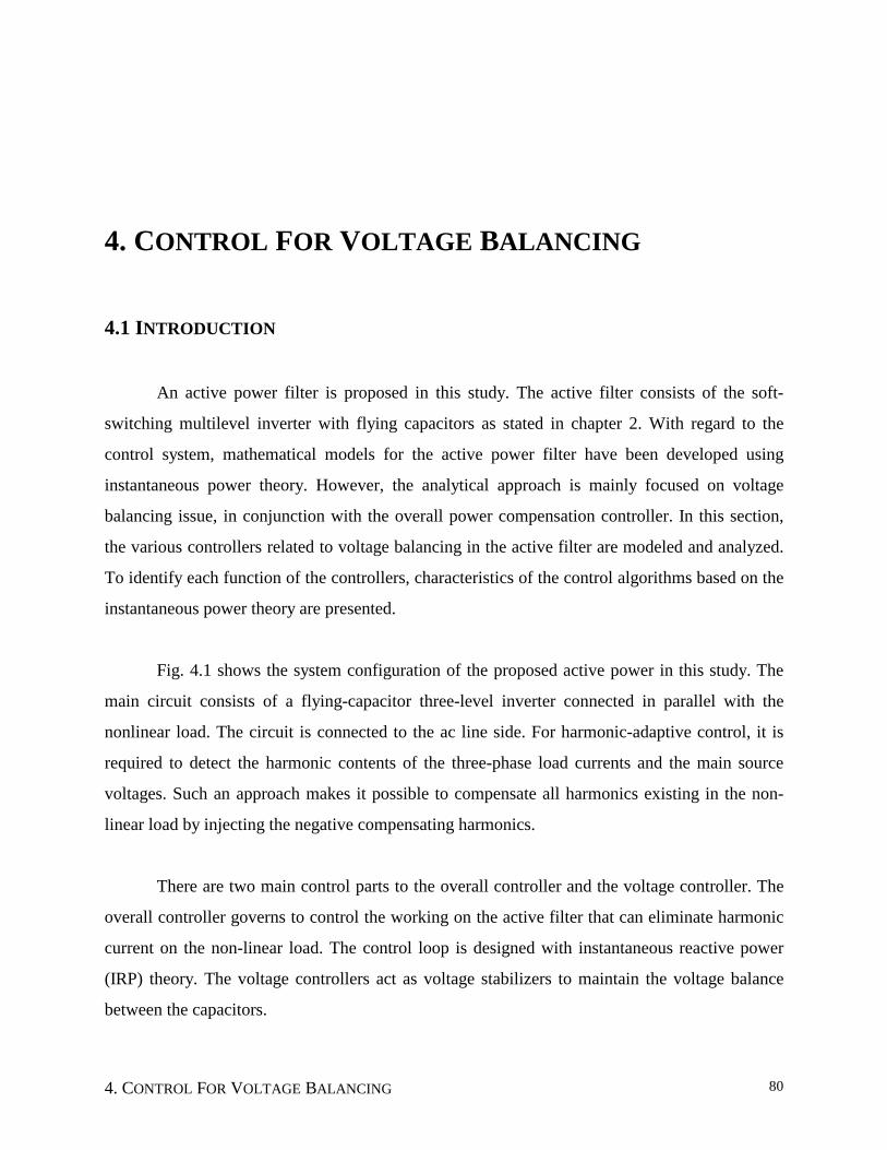
Fig. 4.1 shows the system configuration of the proposed active power in this study. The
main circuit consists of a flying-capacitor three-level inverter connected in parallel with the
nonlinear load. The circuit is connected to the ac line side. For harmonic-adaptive control, it is
required to detect the harmonic contents of the three-phase load currents and the main source
voltages. Such an approach makes it possible to compensate all harmonics existing in the non-
linear load by injecting the negative compensating harmonics.
There are two main control parts to the overall controller and the voltage controller. The
overall controller governs to control the working on the active filter that can eliminate harmonic
current on the non-linear load. The control loop is designed with instantaneous reactive power
(IRP) theory. The voltage controllers act as voltage stabilizers to maintain the voltage balance
between the capacitors.
4. CONTROL FOR VOLTAGE BALANCING 81
NonlinearLoad
Lf
iC
iLis
vas
S1a
va vb Cdc
0
vc
S2a
S1b
S2b
S1c
S2c
S1a
va vb Cdc
0
vc
S2a
S1b
S2b
S1c
S2c
vbs vcs
iC*
Switching Patterns
IRP Control
iL
vs
iC
Vdc*
Current Control
AC Source
_
1aS
_
2aS
_
1bS
_
2bS
_
1cS
_
2cSKvcf
( )s
KsK IVcfPVcf +
( )s
KsK IV d cP V d c +*Cp∆
Kvdc
Vdc
VCf
VCf*+
+
-
-
α∆±TMS320C32 DSP board
Active Filter
Fig. 4.1. Proposed three-level active power filter with flying capacitors.
4.2 INSTANTANEOUS REACTIVE POWER (IRP) CONTROL
Various approaches have been used to calculate the suitable compensating current
references [B1], [B4], [B6], [B10], [B12], and [B19]. Among them, instantaneous reactive power
(IRP) control that is well known as p-q algorithm presented by Akagi is widely used in active
power applications [B12]. In this study the IRP control algorithm is considered. This algorithm is
suitable for balanced source voltages and nonlinear loads, and directly controls the source current
to compensate the current harmonics and the power factor at the same time.
To define an IRP theory, a three-phase power circuit is modeled below:
4. CONTROL FOR VOLTAGE BALANCING 82
�
���
�
�
=
cs
bs
as
s
vvv
v and �
���
�
�
=
Lc
Lb
La
L
iii
i (4-1)
where, vas, vbs, and vcs are the instantaneous source voltages and iLa, iLb, and iLc are the
instantaneous load currents. To calculate the instantaneous power, the three-phase source
voltages and the three-phase load currents are transformed into the α-β orthogonal coordinates.
The α-β transformation is applied to the source voltages and the load currents, respectively.
Accordingly, the space vectors are defined by:
[ ]�
���
�
�
⋅=��
��
�=
cs
bs
as
s
vvv
Cvv
vβ
α and [ ]����
���
�
�
⋅=��
��
�=
Lc
Lb
La
L
iii
Cii
iβ
α (4-2)
where,
[ ] ���
�
−−−
⋅=2/32/30
2/12/1132C
The instantaneous active power and imaginary power are calculated from the α-β
orthogonal coordinates. These instantaneous powers are filtered to separate ac and dc
components. Here, the dc components are related to the active and reactive powers due to
fundamental voltages and currents. Assume that the instantaneous real power, pL, and
instantaneous imaginary power, qL, on the non-linear load are given by
�
��
���
��
�
−=�
���
�
β
α
αβ
βα
L
L
L
L
ii
vvvv
qp
(4-3)
4. CONTROL FOR VOLTAGE BALANCING 83
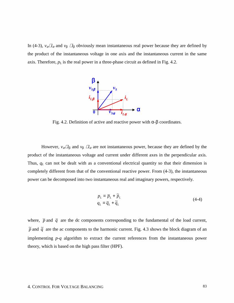
In (4-3), vα⋅ iα and vβ ⋅ iβ obviously mean instantaneous real power because they are defined by
the product of the instantaneous voltage in one axis and the instantaneous current in the same
axis. Therefore, pL is the real power in a three-phase circuit as defined in Fig. 4.2.
αααα
ββββ
0 vSαααα iLαααα
vSββββ
iLββββ
vS
iL
Fig. 4.2. Definition of active and reactive power with α-β coordinates.
However, vα⋅ iβ and vβ ⋅ iα are not instantaneous power, because they are defined by the
product of the instantaneous voltage and current under different axes in the perpendicular axis.
Thus, qL can not be dealt with as a conventional electrical quantity so that their dimension is
completely different from that of the conventional reactive power. From (4-3), the instantaneous
power can be decomposed into two instantaneous real and imaginary powers, respectively.
LLL
LLL
qqqppp
~~
+=+=
(4-4)
where, p and q are the dc components corresponding to the fundamental of the load current,
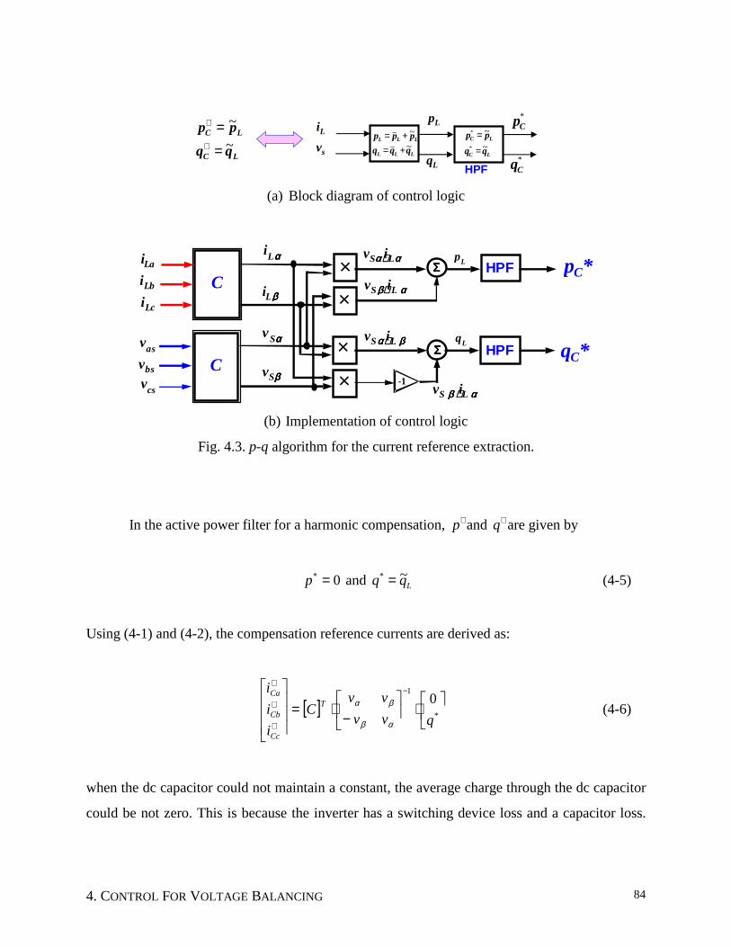
p~ and q~ are the ac components to the harmonic current. Fig. 4.3 shows the block diagram of an
implementing p-q algorithm to extract the current references from the instantaneous power
theory, which is based on the high pass filter (HPF).
4. CONTROL FOR VOLTAGE BALANCING 84
LC
LC
qqpp
~
~
=
=∗
∗ iL
vs
pL
qLLLL
LLL
qqqppp
~~
+=+=
HPFLC
LC
qqpp~
~*
*
=
=
*Cp
*Cq
(a) Block diagram of control logic
iLa
iLb
iLc
C
iLαααα
iLββββ
vas
vbsvcs
C
vSαααα
vSββββ -1
××
×
×
vSα⋅α⋅α⋅α⋅iLαααα
vS α⋅α⋅α⋅α⋅iL ββββ
vS β⋅β⋅β⋅β⋅ iL αααα
vS ββββ ⋅⋅⋅⋅iL αααα
ΣΣΣΣ
ΣΣΣΣ
pL
qL
HPF
HPF
pC*
qC*
(b) Implementation of control logic
Fig. 4.3. p-q algorithm for the current reference extraction.
In the active power filter for a harmonic compensation, ∗p and ∗q are given by
0* =p and Lqq ~* = (4-5)
Using (4-1) and (4-2), the compensation reference currents are derived as:
[ ] ���
�⋅��
��
�
−⋅=
����
���
�
� −
∗
∗
∗
*
10qvv
vvC
iii
T
Cc
Cb
Ca
αβ
βα (4-6)
when the dc capacitor could not maintain a constant, the average charge through the dc capacitor
could be not zero. This is because the inverter has a switching device loss and a capacitor loss.
4. CONTROL FOR VOLTAGE BALANCING 85
To meet the charge balance, some real power is delivered to the dc capacitors by controlling a dc
voltage loop of the inverter. Thus, an additional instantaneous real power, ∆p, should be
compensated as
[ ] ���
�∆⋅��
��
�
−⋅=
����
���
�
� −
∗
∗
∗
*
1
qp
vvvv
Ciii
T
Cc
Cb
Ca
αβ
βα (4-7)
where, ∆p is the instantaneous real power necessary to compensate the voltage across the dc
capacitor to the reference value.
4.3 CURRENT CONTROL
The use of a current control loop has several benefits for an active filter. First, if the
active filter is used to inject the current harmonics into the power networks, the current command
is applied to the current loop to achieve the desired compensating current. Second, a current loop
provides an overcurrent protection, when the active filter currents are sensed and limited to a
maximum value. Third, for advance control, it is necessary to have a current control loop, which
follows the nonlinear current command. Once the linearized model of an active filter is identified
with a plant, the current controller is designed to generate harmonic reference currents for the
three-phase system.
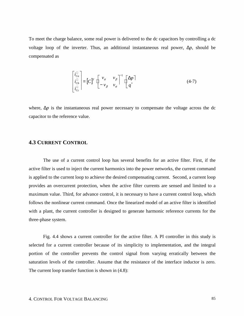
Fig. 4.4 shows a current controller for the active filter. A PI controller in this study is
selected for a current controller because of its simplicity to implementation, and the integral
portion of the controller prevents the control signal from varying erratically between the
saturation levels of the controller. Assume that the resistance of the interface inductor is zero.
The current loop transfer function is shown in (4.8):
4. CONTROL FOR VOLTAGE BALANCING 86
IicaPWMPicaCPWMPicaCf
IicaPWMPicaCPWMPicaC
Ca
CaC KKKHsKKHsL
KKKHsKKHsisisG
+++== 2* )(
)()( (4-8)
where,
KPica : the proportional gain in a-phase current
KIica : the integral gain in a-phase current
KPWM : the PWM gain of the active filter
HC : the current sensor gain in a-phase current
Lf : the interface inductance of the inductor
+
-
∗∗∗∗Cai
CM DCai _
CaisLf
1s
KsKC aC a IiP i )( ++++
PI Ctrl Limiter
P W MK
Inverter Interface Inductor
CH
Current Transducer
Fig. 4.4. A current control loop for active filter.
With this control diagram in Fig. 4.4, the current loop becomes a second order system in
which second order system design techniques are applied. In designing the current controller
gains, it is desirable to specify a bandwidth for the current loop based on the switching frequency
of the active filter. Considering the fast bandwidth of the current loop, the characteristic equation
of the approximated current loop is derived. Moreover, since it is a second-order equation, the
natural frequency, ωn, and damping ratio, ξ, can be used to obtain the current controller gain and
4. CONTROL FOR VOLTAGE BALANCING 87
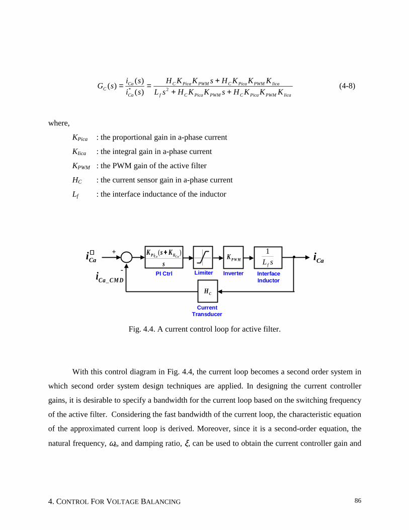
time constant. Below, (4-9) and (4-10) specify the damping ratio and the natural frequency of the
approximated system.
22
2
2)(
nn
n
sssH
ωξωω
++++++++==== (4-9)
where,
1)21()21(
2
222
2
++++=
=
=
ξξ
ωω
ω
ξω
cn
PicaPWMC
fnIi
PWMC
fnPi
KKHL
K
KHL
K
Ca
Ca
�
(4-10)
From (4-9) and (4-10), the P and I gains can be derived for a given natural frequency and
damping ratio. In order to evaluate the frequency response of the system, the bandwidth of the
closed-loop transfer function can be founded. Once the gains of the current controller are found,
an unapproximated current loop is simulated by using Bode plots. Based on the load condition
with an interface inductor, PI gains are calculated considering the desired specifications with Vdc
= 750V, Lf = 1 mH, and Vref = 5V. Considering the switching frequency of 12 kHz, the bandwidth
of the controller is selected as 1.2 kHz. The controller has been designed with the following
parameters:
KPWM =Vdc/Vref = 150
HC = iCa*/iCa = 0.05
ξ = 1
KPica = 2.01
KIica = 3771
Lf = 1mF
4. CONTROL FOR VOLTAGE BALANCING 88
Therefore, the transfer functions of the PI controller is
( )ss
ssGCPI758001.2)3771(01.2 +=+= (4-11)
With (4-11) and the feedback path, the open-loop transfer function or the loop transfer function,
GH (s), can be derived as:
( ) 2000,850,56075,151)758001.2(
ssH
sLK
ssGH C
fPWM
+=⋅⋅⋅+= (4-12)
where, GH(s) is the product term in the system transfer function of the forward path and the
feedback path. To find the magnitude and phase margin of the open-loop transfer function, the
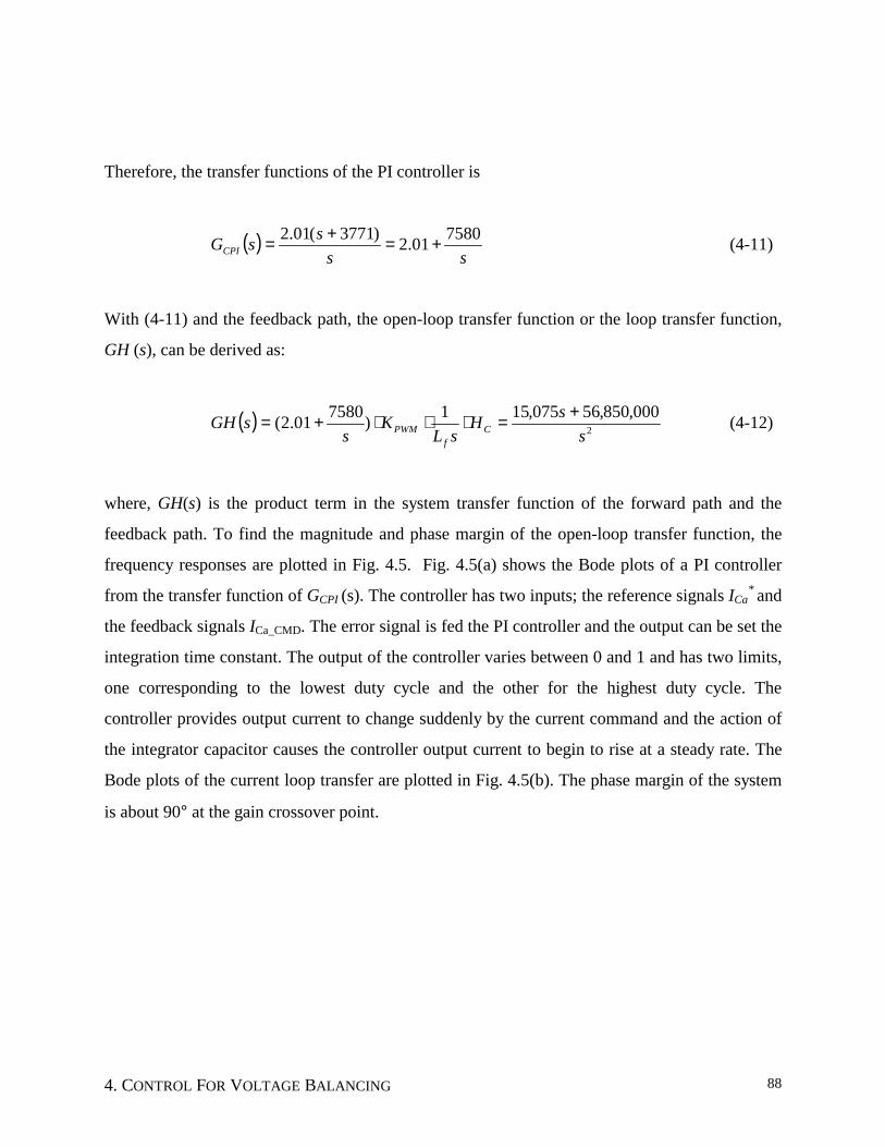
frequency responses are plotted in Fig. 4.5. Fig. 4.5(a) shows the Bode plots of a PI controller
from the transfer function of GCPI (s). The controller has two inputs; the reference signals ICa* and
the feedback signals ICa_CMD. The error signal is fed the PI controller and the output can be set the
integration time constant. The output of the controller varies between 0 and 1 and has two limits,
one corresponding to the lowest duty cycle and the other for the highest duty cycle. The
controller provides output current to change suddenly by the current command and the action of
the integrator capacitor causes the controller output current to begin to rise at a steady rate. The
Bode plots of the current loop transfer are plotted in Fig. 4.5(b). The phase margin of the system
is about 90° at the gain crossover point.
4. CONTROL FOR VOLTAGE BALANCING 89
101
102
103
104
105
-100
-80
-60
-40
-20
0
Frequency (radians)
101
102
103
104
105
100
101
102
103
Frequency (radians)
Mag
nitu
dePh
ase
(deg
rees
)M
agni
tude
(a) Proportional-integral (PI) controller
101
102
103
104
105
-180
-160
-140
-120
-100
-80
Fre que ncy (ra dia ns )
101
102
103
104
105
10-5
100
105
Fre que ncy (ra dia ns )
gPh
ase
(deg
rees
)M
agni
tude
(b) Open-loop system
Fig. 4.5. Bode plots of an open-loop current control system with proportional-integral control.
4. CONTROL FOR VOLTAGE BALANCING 90
4.4 DC BUS CAPACITOR VOLTAGE CONTROL
The most commonly used techniques for dc bus capacitor voltage control are the PI
controller and PWM. The dc bus voltage control allows the dc capacitor voltage to have a
constant value. When the capacitor does not maintain a constant, the average charge through the
dc capacitor does not equal zero. This is because the inverter has switching a device loss and a
capacitor loss during operations. Furthermore, the size of the dc bus capacitor depends on the
magnitude of ripple voltage and capacitor current. For example, when the filter current is
positive, the capacitor is charged. When the filter current is negative, the capacitor is discharged.
During charging and discharging, the charging frequency is twice the line frequency.
On the other hand, if the transient load change in the active filter occurs, the dc bus
voltage varies. This variation is consequently considered when designing the dc bus capacitor.
Also, in order to stabilize the dc bus voltage, a closed loop control is required.
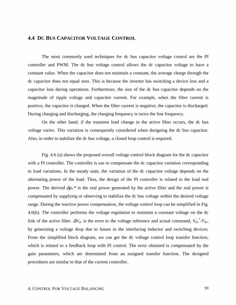
Fig. 4.6 (a) shows the proposed overall voltage control block diagram for the dc capacitor
with a PI controller. The controller is use to compensate the dc capacitor variation corresponding
to load variations. In the steady state, the variation of the dc capacitor voltage depends on the
alternating power of the load. Thus, the design of the PI controller is related to the load real
power. The derived ∆pC* is the real power generated by the active filter and the real power is
compensated by supplying or observing to stabilize the dc bus voltage within the desired voltage
range. During the reactive power compensation, the voltage control loop can be simplified in Fig.
4.6(b). The controller performs the voltage regulation to maintain a constant voltage on the dc
link of the active filter. ∆Vdc is the error to the voltage reference and actual command, Vdc*-Vdc,
by generating a voltage drop due to losses in the interfacing inductor and switching devices.
From the simplified block diagram, we can get the dc voltage control loop transfer function,
which is related to a feedback loop with PI control. The error obtained is compensated by the
gain parameters, which are determined from an assigned transfer function. The designed
procedures are similar to that of the current controller.
4. CONTROL FOR VOLTAGE BALANCING 91
+
-
∗dcv
CM Ddcv _
Cai
sKsK
C aC f IvPv )( ++++*Cp∆∆∆∆
dcv∆
iLabc abc/αβαβαβαβ
iLαααα
iLββββ
vabcsvSαααα
vSββββ
pL
qL
HPF
LC
LC
qqpp~~
*
*
==
*Cp
*Cq
abc/αβαβαβαβ
αβαβαβαβ/
abc
iCαααα*
iCββββ*
iCa*
+
+
P=
f( i,v)iC*=
f( p,v-1)**CC pp ∆∆∆∆++++
GC(s)
iLabc abc/αβαβαβαβ
iLαααα
iLββββ
vabcsvSαααα
vSββββ
pL
qL
HPF
LC
LC
qqpp~~
*
*
==
LC
LC
qqpp~~
*
*
==
*Cp*Cp
*Cq*Cq
abc/αβαβαβαβ
αβαβαβαβ/
abc
iCαααα*
iCββββ*
iCa*
+
+
P=
f( i,v)iC*=
f( p,v-1)**CC pp ∆∆∆∆++++ **CC pp ∆∆∆∆++++
GC(s)
sCK
d
VH
dcv (a) Overall voltage control loop
+
-
∗dcv
CM Ddcv _
Cai
sKsK
C aC f IvPv )( +*Cp∆
dcv∆
sCK
d
VH
dcvGC (s)
*Cai
G (s)
(b) Simplified voltage control loop
Fig. 4.6. Voltage control loop for dc bus capacitor.
4.5 FLYING CAPACITOR VOLTAGE CONTROL
In the proposed active filter, the voltage unbalance of the flying capacitor in practical
implementations was observed due to unequal parameters of the inverter. Thus, a voltage
4. CONTROL FOR VOLTAGE BALANCING 92
controller is necessary to maintain a constant value of the voltage source across the flying
capacitor. With regard to the control schemes for voltage balancing, there are various
compensating approaches for the three-phase active power filters with PWM control as follows:
- Direct switching states control,
- Sliding mode control,
- Hystersis control,
- PI control with duty-cycle changing, etc.
Furthermore, it is well known that the performances of active power filters highly depend on the
dynamic response corresponding load variations. Thus, it is important to minimize the
calculation processing time to obtain the power compensating references. To reach this end, a
new PI controller with phase-shift is proposed and explored in this section. The controller is
similar to a conventional PI controller with duty-cycle changing. It can achieve a fast dynamic
response of the system in conjunction with a digital controller.
4.5.1 Analysis of Voltage Variations
The current flowing flying capacitor depends on the control index and output current of
the inverter as below.
LcCf Imti ⋅⋅⋅⋅====)( (4-13)
where, mc is the different duty cycle between switching devices and IL is the output rms current.
On the other hand, it depends on the capacitor voltage variations.
dt
dvCti Cf
fCf ====)( (4-14)
4. CONTROL FOR VOLTAGE BALANCING 93
where, Cf is the flying capacitance of the flying capacitor. Substituting (4-13) into (4-14), thus,
leads to (4-15).
f
LcCf
CIm
dttdv
====)(
(4-15)
This result indicates that variations of capacitor voltage are governed by the nonlinear first order
differential equations. From (4-15), the capacitor voltage variation can be derived as below.
swf
LcCf fC
Imv⋅⋅⋅⋅⋅⋅⋅⋅====∆ (4-16)
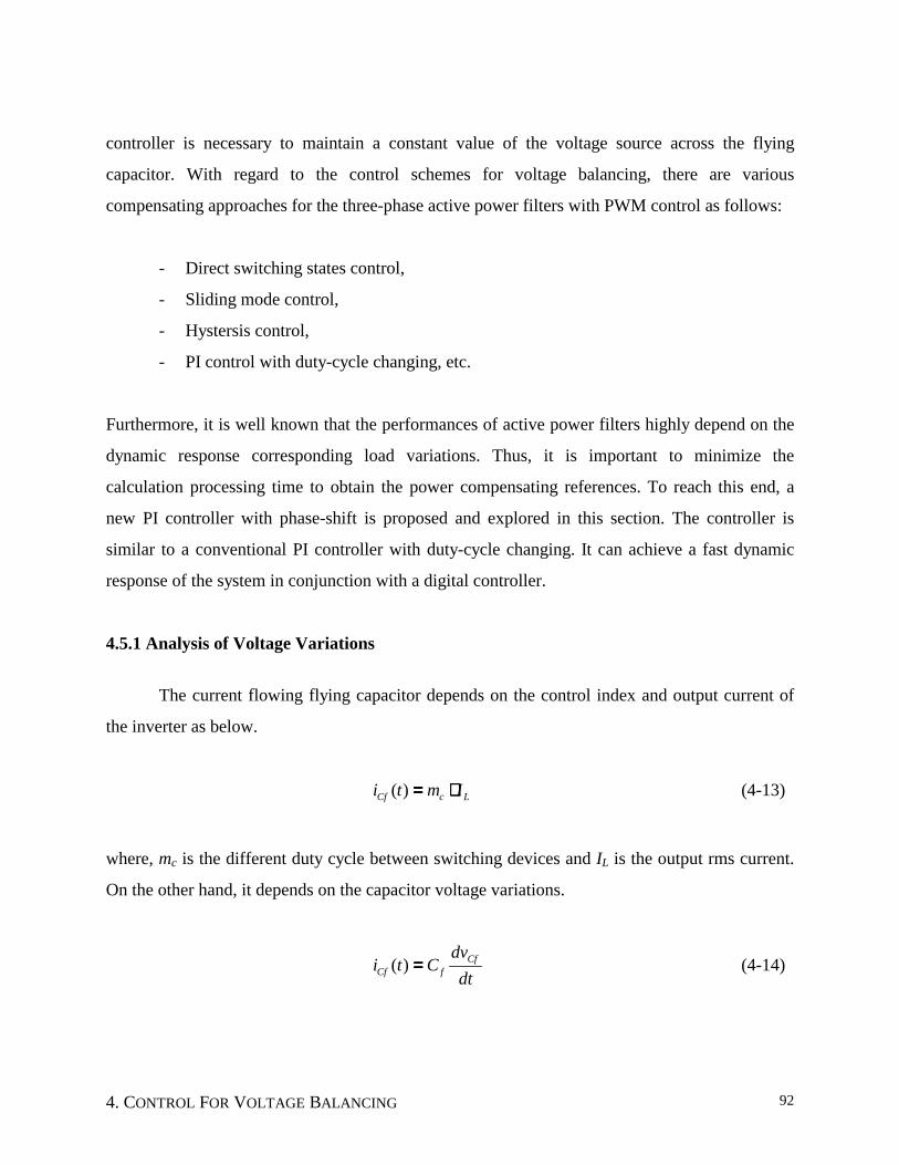
From (4-16), the voltage loop transfer function can be derived. By controlling the polarity of mc
in Fig. 4.6, the flying capacitor voltage can be stabilized as shown in Fig. 4.7, where ± ∆ mc
depends on the inverter parameters.
21 dd >>>>VS /2
21 dd <<<<
: Charging
: Discharging
VCf
0 t
d1 = d2 ±±±± ∆∆∆∆mc : Controllablevoltage
Fig. 4.7. Voltage control for balancing.
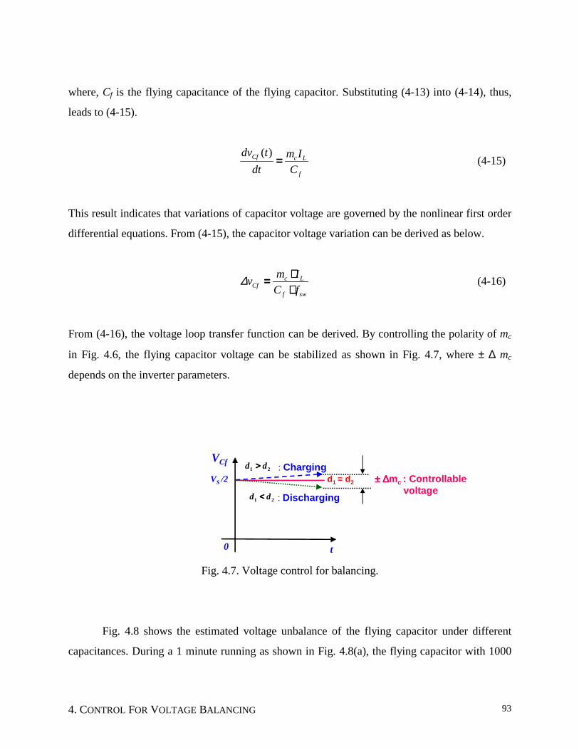
Fig. 4.8 shows the estimated voltage unbalance of the flying capacitor under different
capacitances. During a 1 minute running as shown in Fig. 4.8(a), the flying capacitor with 1000
4. CONTROL FOR VOLTAGE BALANCING 94
µF was decreased to 285V for mc = 0.05 and 297 V for mc = 0.01, respectively. However, with
200 µF, the voltage was also decreased to 225 V for mc = 0.05 and 285 V for mc = 0.01,
respectively. As a result, this indicates that a change in the difference of duty cycle between two
cells, mc (= d1 - d2), creates a large change in VCf, when Cf is small.
0 10 20 30 40 50 60220
240
260
280
300
320320
220
Vcf1 t( )
Vcf t( )
600 t
mC =0.01
mC =0.05
Cf =1000µF
VCf
T (sec) 0 10 20 30 40 50 60
220
240
260
280
300
320320
220
Vcf2 t( )
Vcf3 t( )
600 t
mC =0.01
mC =0.05
Cf =200µF
VCf
T (sec) (a) Cf = 1000 µF (b) Cf = 200 µF
Fig. 4.8. Estimated voltage unbalance of the clamping capacitor during inverter operation.
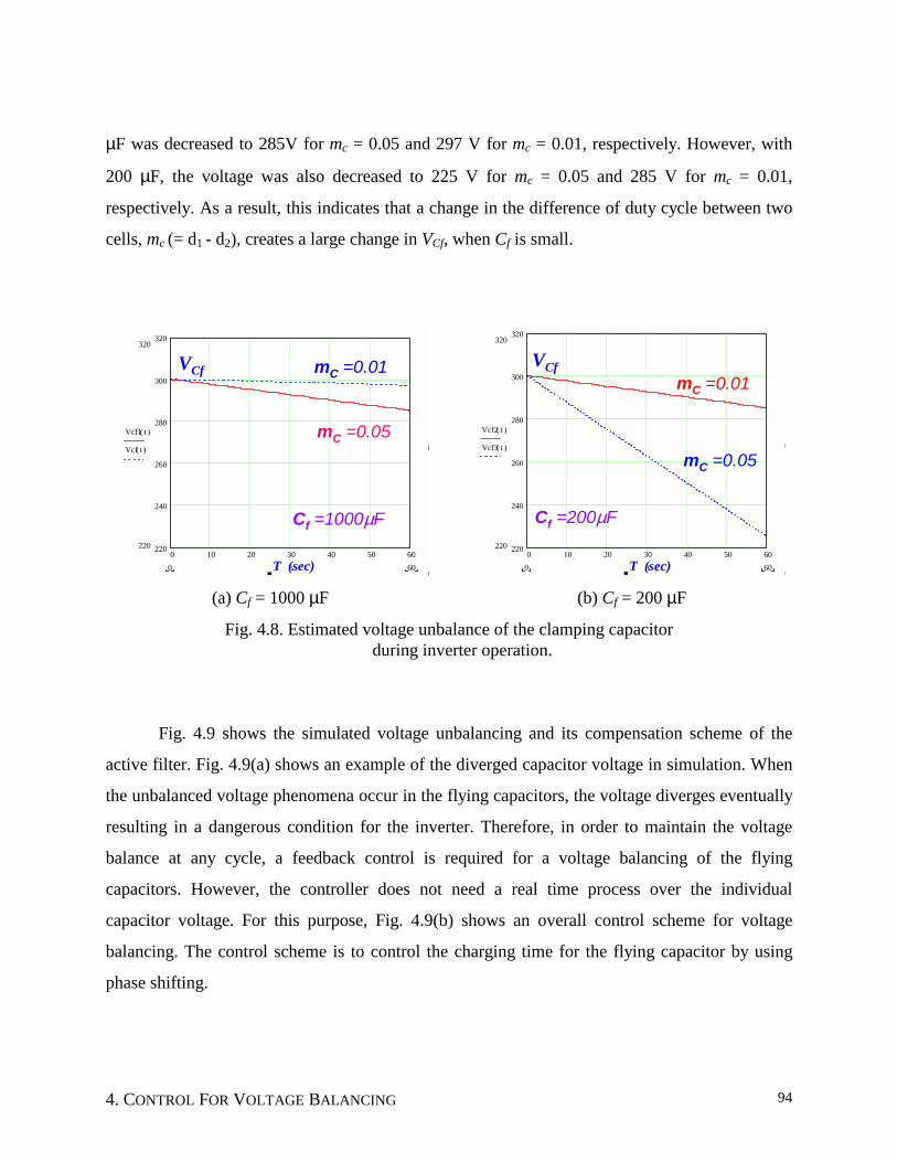
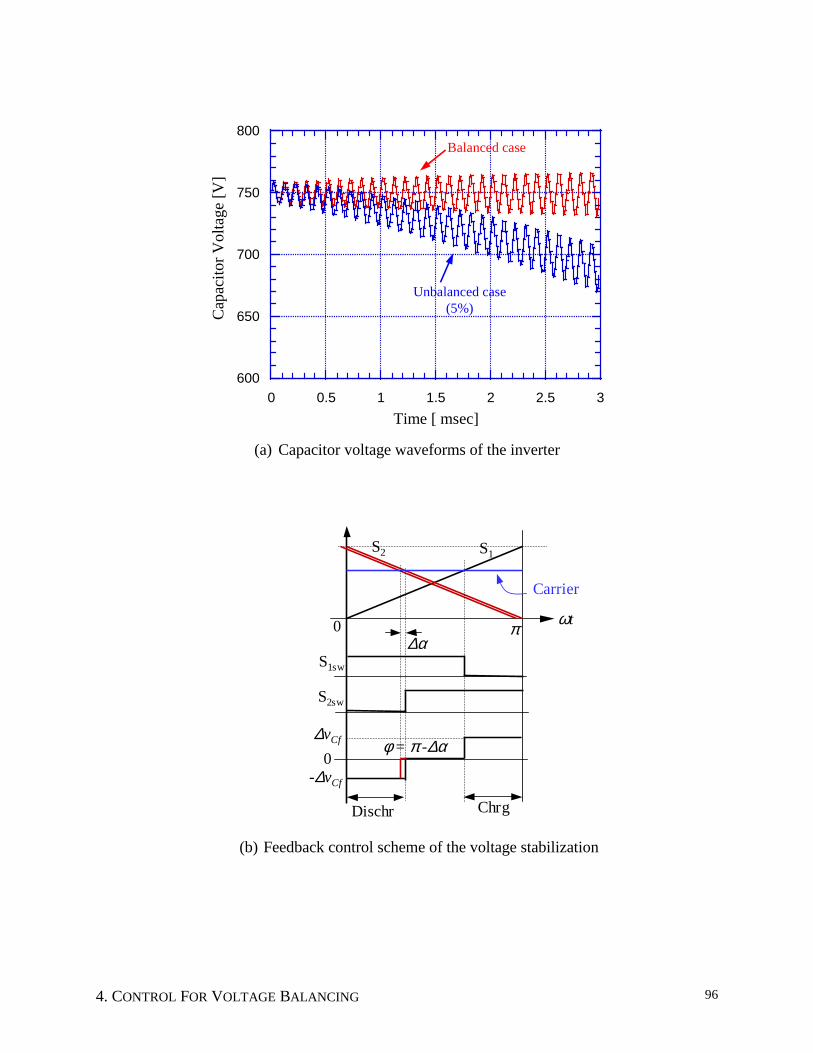
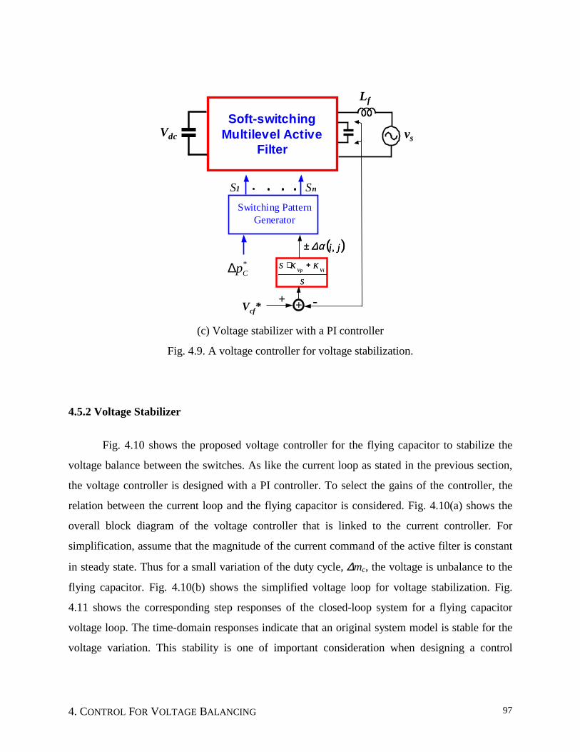
Fig. 4.9 shows the simulated voltage unbalancing and its compensation scheme of the
active filter. Fig. 4.9(a) shows an example of the diverged capacitor voltage in simulation. When
the unbalanced voltage phenomena occur in the flying capacitors, the voltage diverges eventually
resulting in a dangerous condition for the inverter. Therefore, in order to maintain the voltage
balance at any cycle, a feedback control is required for a voltage balancing of the flying
capacitors. However, the controller does not need a real time process over the individual
capacitor voltage. For this purpose, Fig. 4.9(b) shows an overall control scheme for voltage
balancing. The control scheme is to control the charging time for the flying capacitor by using
phase shifting.
4. CONTROL FOR VOLTAGE BALANCING 95
The basic idea is to convert from ∆mc to the phase shifting angle, ∆α. First, each
capacitor voltage VCf(i,j) is measured with respect to the reference dc voltage Vdc*. Then, the
voltage error is used for the slight adjustment of phase shift of the switching pattern through the
control window (± ∆ α (i,j)) of the ith and jth levels. The sign of the phase-shift adjustment
depends on the charging voltage balance through the operating window (∆ α(i,j)) so that the
VCf(i,j) is controlled to the desired voltage level. After the voltage reaches the equalized voltage,
the switching pattern has a normal operation function. This approach results in the same effects
to adjust the duty cycle on the controller. However, this approach is limited to the digital
controller, which uses a conversion table as the look-up table. For implementation, a digital
proportional-integral (PI) controller as shown in Fig. 4.9(c) can be used to solve the voltage
unbalance problem. Basically, whenever the voltage unbalance happens, the switching pattern of
the inverter should be controlled with an immediate phase-shifting adjustment by triggering the
control window.
4. CONTROL FOR VOLTAGE BALANCING 96
600
650
700
750
800
0 0.5 1 1.5 2 2.5 3Time [ msec]
Cap
acito
r Vol
tage
[V]
Unbalanced case(5%)
Balanced case
(a) Capacitor voltage waveforms of the inverter
ChrgDischr
S1S2
Carrier
0 ωt∆α
S1sw
S2sw
∆vCf
-∆vCf
0φ= π -∆α
π
(b) Feedback control scheme of the voltage stabilization
4. CONTROL FOR VOLTAGE BALANCING 97
Vdc
Soft-switching Multilevel Active
Filter
S1 Sn
Switching Pattern Generator
( )j,iα∆± ( )j,iα∆±
+ -+
S
KKSViVp
+⋅
S
KKSViVp
+⋅
Vcf*
Lf
*Cp∆
vs
(c) Voltage stabilizer with a PI controller
Fig. 4.9. A voltage controller for voltage stabilization.
4.5.2 Voltage Stabilizer
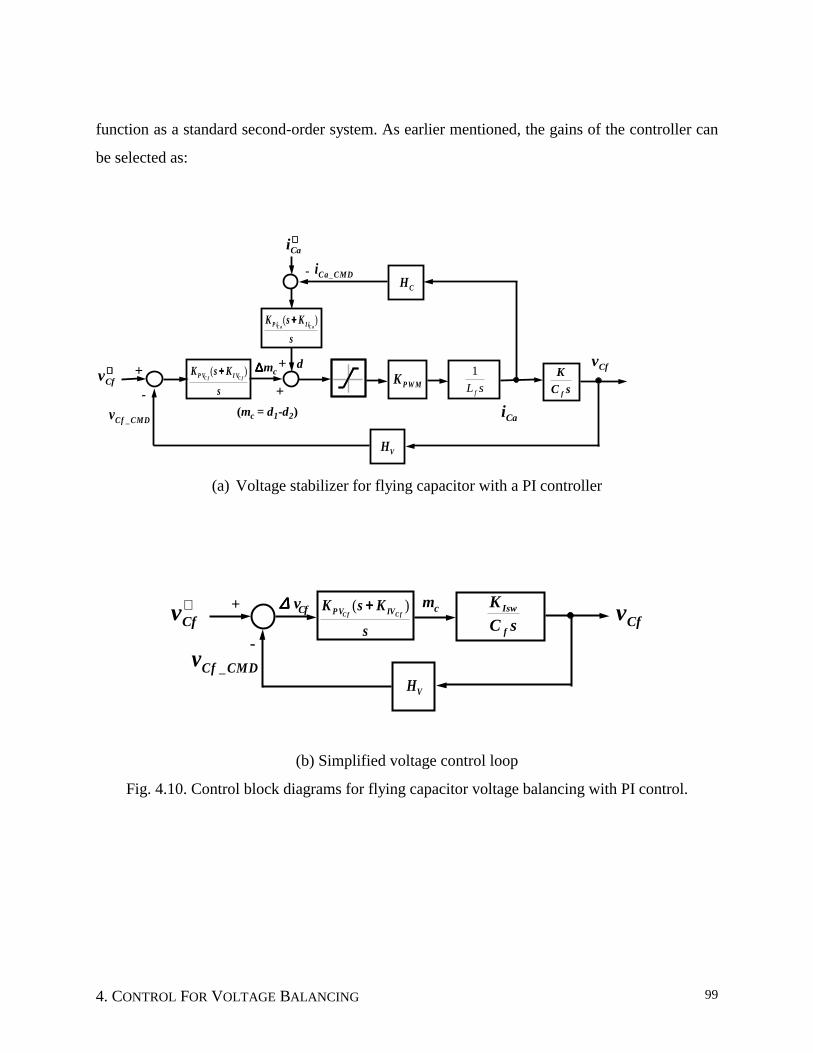
Fig. 4.10 shows the proposed voltage controller for the flying capacitor to stabilize the
voltage balance between the switches. As like the current loop as stated in the previous section,
the voltage controller is designed with a PI controller. To select the gains of the controller, the
relation between the current loop and the flying capacitor is considered. Fig. 4.10(a) shows the
overall block diagram of the voltage controller that is linked to the current controller. For
simplification, assume that the magnitude of the current command of the active filter is constant
in steady state. Thus for a small variation of the duty cycle, ∆mc, the voltage is unbalance to the
flying capacitor. Fig. 4.10(b) shows the simplified voltage loop for voltage stabilization. Fig.
4.11 shows the corresponding step responses of the closed-loop system for a flying capacitor
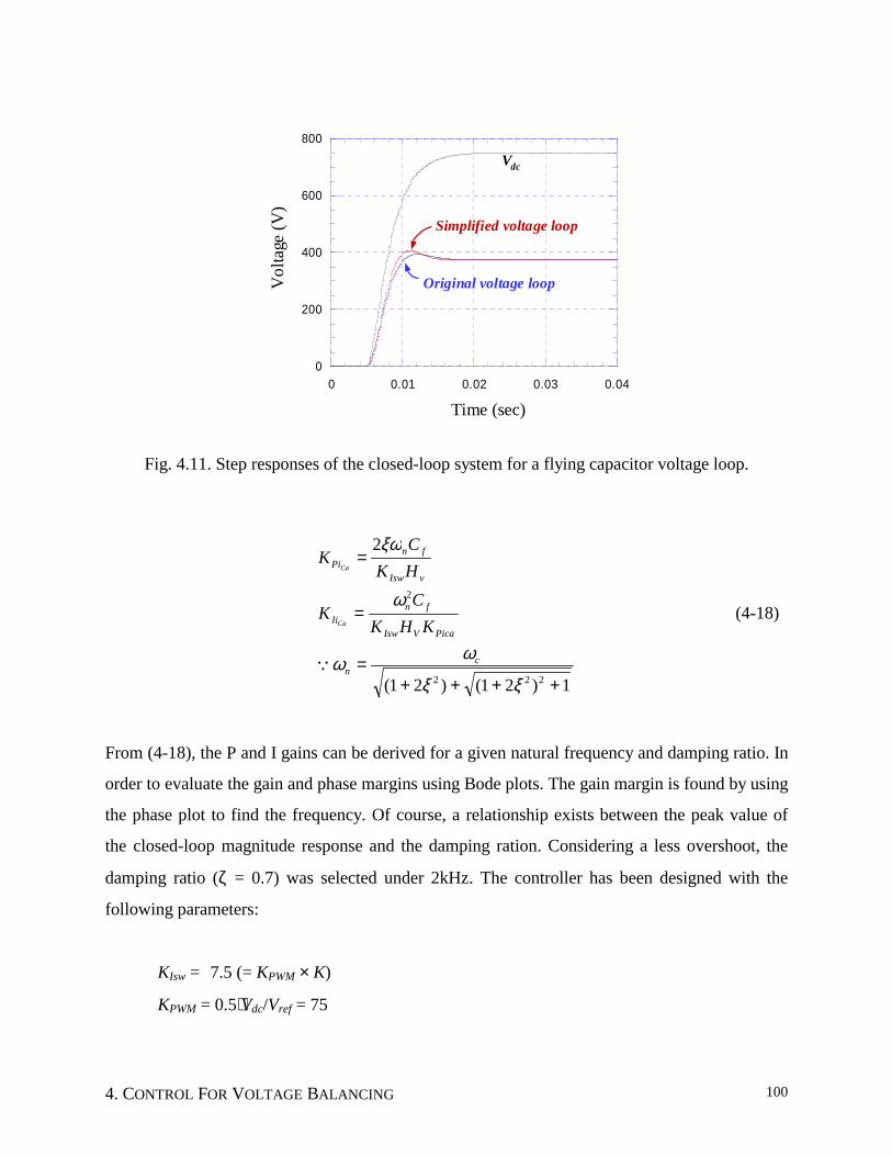
voltage loop. The time-domain responses indicate that an original system model is stable for the
voltage variation. This stability is one of important consideration when designing a control
4. CONTROL FOR VOLTAGE BALANCING 98
system. Since the system is stable, then its relative stability can be simplified to design the
controller to reduce the calculation time to find the compensation parameters. On the other hand,
a simplified block diagram as shown in Fig. 4.10(b) represents the control system for simplicity.
The interpretation of the simplified model is that due to high forward gain in the switching
amplifier, its response is determined by the feedback. Simulation results in Fig. 4.11 show that
the modified model is very close to the original control system, even the system has a small
overshoot. The rise time of the modified model is a little fast and the time response reaches the
final steady state. It concludes that the simplified mode is valid for voltage control. The
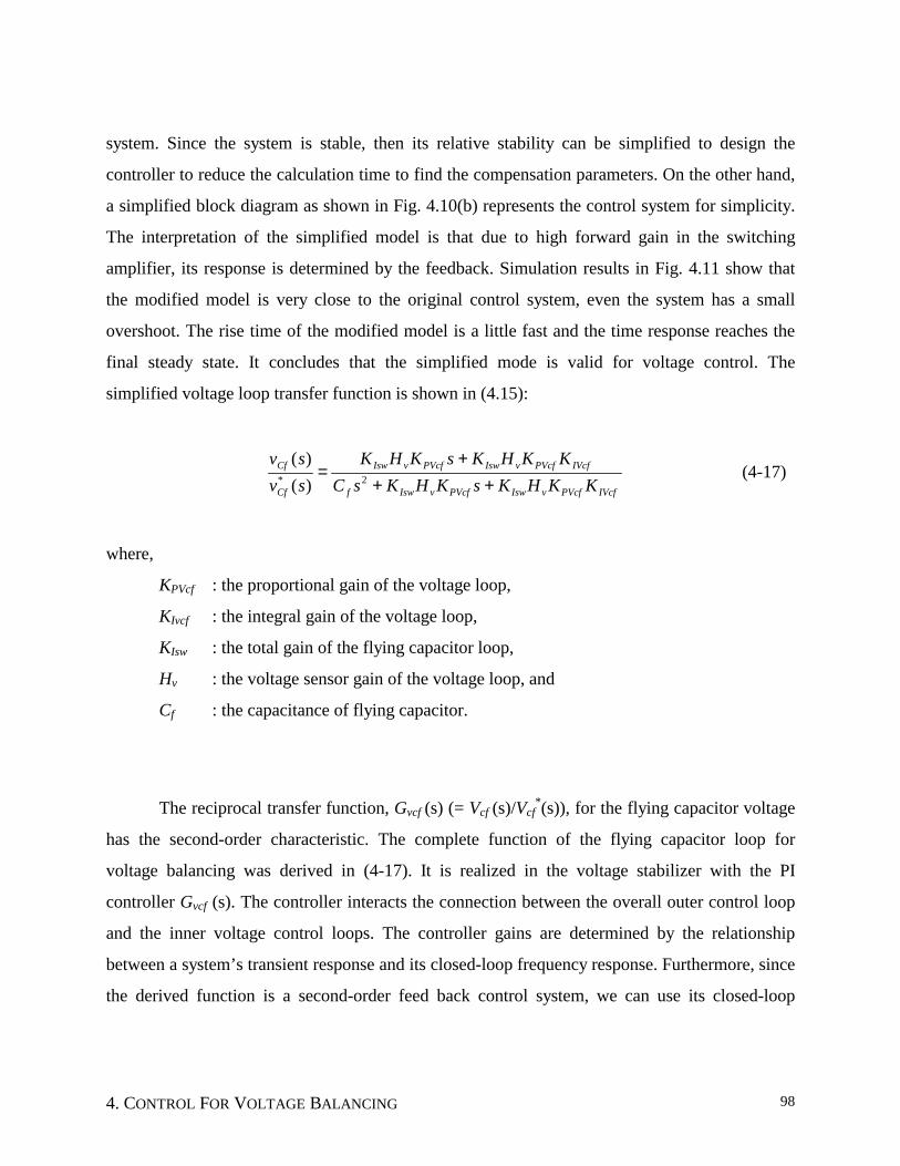
simplified voltage loop transfer function is shown in (4.15):
IVcfPVcfvIswPVcfvIswf
IVcfPVcfvIswPVcfvIsw
Cf
Cf
KKHKsKHKsCKKHKsKHK
svsv
+++
= 2* )()(
(4-17)
where,
KPVcf : the proportional gain of the voltage loop,
KIvcf : the integral gain of the voltage loop,
KIsw : the total gain of the flying capacitor loop,
Hv : the voltage sensor gain of the voltage loop, and
Cf : the capacitance of flying capacitor.
The reciprocal transfer function, Gvcf (s) (= Vcf (s)/Vcf*(s)), for the flying capacitor voltage
has the second-order characteristic. The complete function of the flying capacitor loop for
voltage balancing was derived in (4-17). It is realized in the voltage stabilizer with the PI
controller Gvcf (s). The controller interacts the connection between the overall outer control loop
and the inner voltage control loops. The controller gains are determined by the relationship
between a system’s transient response and its closed-loop frequency response. Furthermore, since
the derived function is a second-order feed back control system, we can use its closed-loop
4. CONTROL FOR VOLTAGE BALANCING 99
function as a standard second-order system. As earlier mentioned, the gains of the controller can
be selected as:
+
∗∗∗∗Cai
CMDCai _
CaisLf
1
sKsK
C aC a I iP i )( ++++
P W MK
CH
sCK
f
+
+
d
VH
sKsK
C fC f I VP V )( ++++∗∗∗∗Cfv
Cfv
-
-
CMDCfv _(mc = d1-d2)
∆∆∆∆mc
(a) Voltage stabilizer for flying capacitor with a PI controller
+
-
∗Cfv
CMDCfv _
CfvsCK
f
Isw
sKsK
C fC f IVP V )( ++++
VH
mc∆∆∆∆ vCf
(b) Simplified voltage control loop
Fig. 4.10. Control block diagrams for flying capacitor voltage balancing with PI control.
4. CONTROL FOR VOLTAGE BALANCING 100
0
200
400
600
800
0 0.01 0.02 0.03 0.04
Vdc
Simplified voltage loop
Original voltage loop
Time (sec)
Vol
tage
(V)
Fig. 4.11. Step responses of the closed-loop system for a flying capacitor voltage loop.
1)21()21(
2
222
2
++++=
=
=
ξξ
ωω
ω
ξω
cn
PicaVIsw
fnIi
vIsw
fnPi
KHKC
K
HKC
K
Ca
Ca
�
(4-18)
From (4-18), the P and I gains can be derived for a given natural frequency and damping ratio. In
order to evaluate the gain and phase margins using Bode plots. The gain margin is found by using
the phase plot to find the frequency. Of course, a relationship exists between the peak value of
the closed-loop magnitude response and the damping ration. Considering a less overshoot, the
damping ratio (ζ = 0.7) was selected under 2kHz. The controller has been designed with the
following parameters:
KIsw = 7.5 (= KPWM × K)
KPWM = 0.5⋅Vdc/Vref = 75
4. CONTROL FOR VOLTAGE BALANCING 101
K = 0.1
HV = VCf*/VCf = 0.01
KCf = 1
KPica = 3.36
KIica = 63
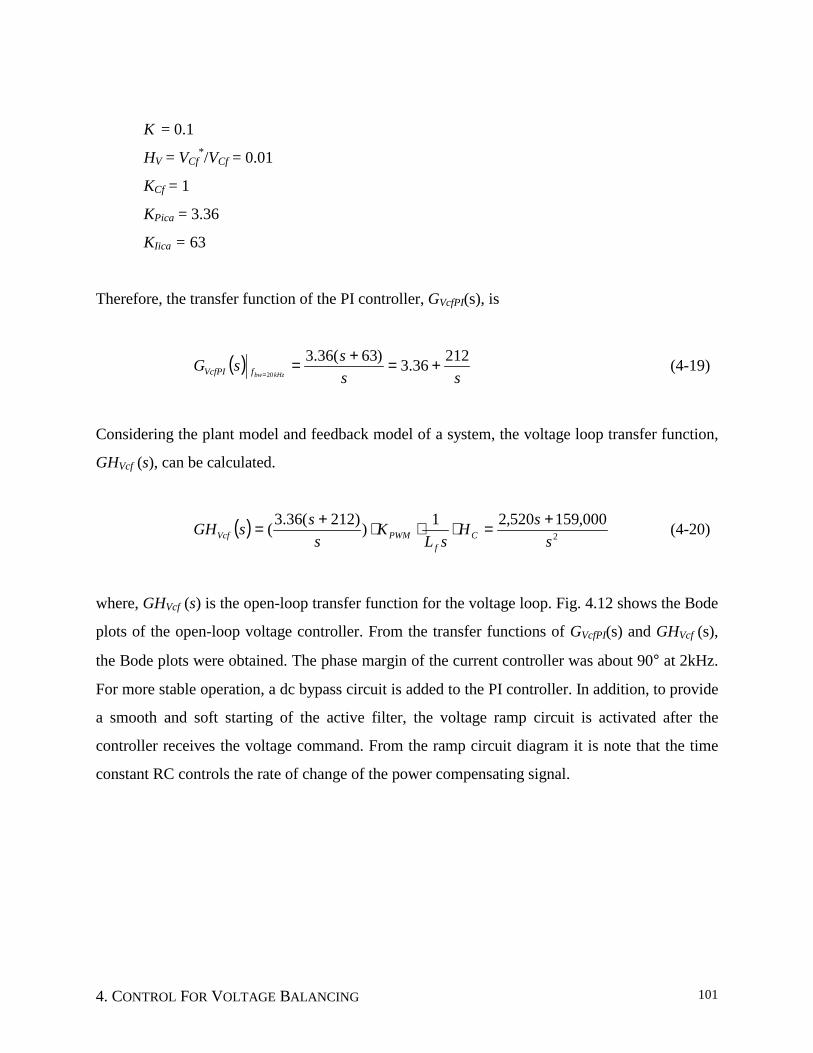
Therefore, the transfer function of the PI controller, GVcfPI(s), is
( )ss
ssGkHzbwfVcfPI
21236.3)63(36.320
+=+==
(4-19)
Considering the plant model and feedback model of a system, the voltage loop transfer function,
GHVcf (s), can be calculated.
( ) 2000,159520,21))212(36.3(
ssH
sLK
sssGH C
fPWMVcf
+=⋅⋅⋅+= (4-20)
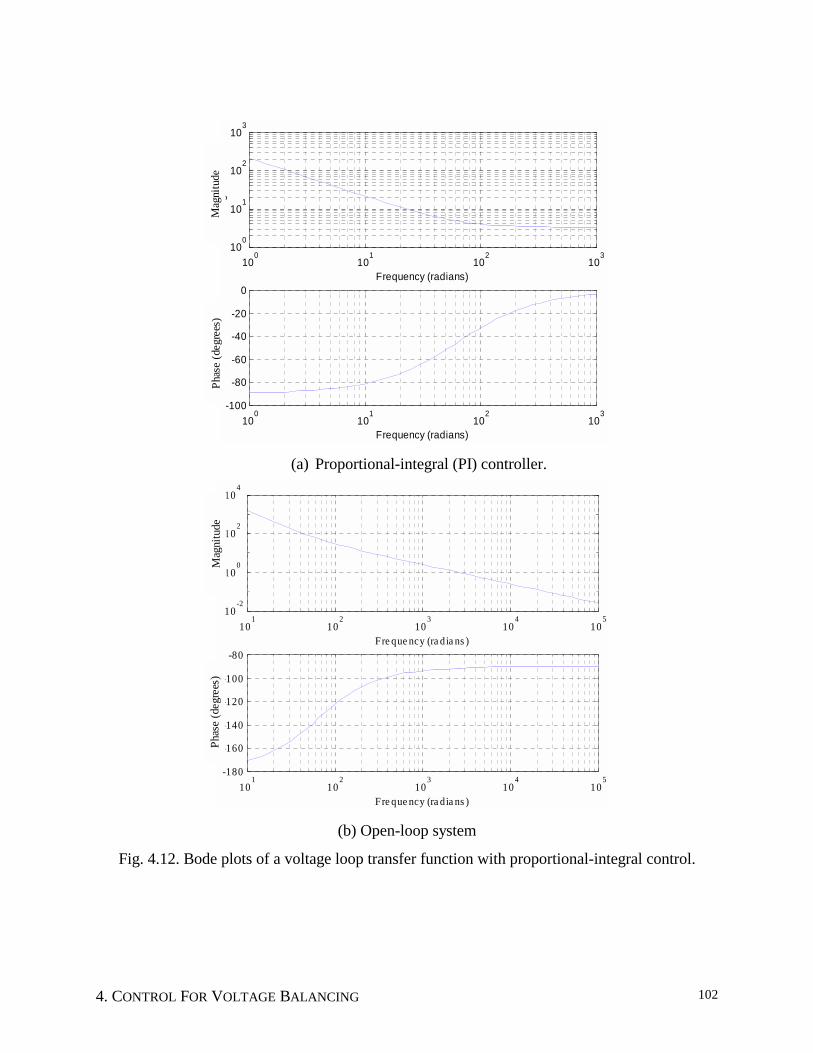
where, GHVcf (s) is the open-loop transfer function for the voltage loop. Fig. 4.12 shows the Bode
plots of the open-loop voltage controller. From the transfer functions of GVcfPI(s) and GHVcf (s),
the Bode plots were obtained. The phase margin of the current controller was about 90° at 2kHz.
For more stable operation, a dc bypass circuit is added to the PI controller. In addition, to provide
a smooth and soft starting of the active filter, the voltage ramp circuit is activated after the
controller receives the voltage command. From the ramp circuit diagram it is note that the time
constant RC controls the rate of change of the power compensating signal.
4. CONTROL FOR VOLTAGE BALANCING 102
100
101
102
103
-100
-80
-60
-40
-20
0
Frequency (radians)
(g
)
100
101
102
103
100
101
102
103
Frequency (radians)
Mag
nitu
dePh
ase
(deg
rees
)M
agni
tude
(a) Proportional-integral (PI) controller.
101
102
103
104
105
-180
-160
-140
-120
-100
-80
Fre que ncy (ra dia ns )
(g
)
101
102
103
104
105
10-2
100
102
104
Fre que ncy (ra dia ns )
Mag
nitu
dePh
ase
(deg
rees
)M
agni
tude
(b) Open-loop system
Fig. 4.12. Bode plots of a voltage loop transfer function with proportional-integral control.
4. CONTROL FOR VOLTAGE BALANCING 103
4.6 CONCLUSION
The new soft-switching multilevel active power filter and its control schemes have been
proposed and discussed in this chapter. To stabilize dc bus voltage and flying capacitor, the
proposed schemes with feedback control loops including main current control and voltage-
balancing control were analyzed and explained.
The dc bus voltage control loop was modeled with a PI controller, which indicates the dc
bus voltage regulator. The controller was considered to the real power flows through the mains,
the non-linear load and power converter to reach a new a balance state. In addition, the controller
compensates the voltage drop due to switching device loss and capacitor loss during operations.
For the flying capacitor voltage balancing, a new PI controller with phase-shift has proposed and
analyzed. The controller acts as the voltage stabilizer to maintain the voltage balance between
flying capacitors and the switching switches. For validation, various numerical simulations were
conducted. In addition, considering a transient load changing, the time responses of the flying
capacitor voltage loop was simulated based on the Laplace transform of the step response of the
system. The controller was stable for the step response. On the other hand, from the transfer
functions of the overall voltage control system, the Bode plots were derived. The gain and phase
margin were derived from the physical block diagram. The validation was discussed with the
gain and the phase magnitudes of the system through simulation results.
To realize the proposed control algorithms, the real time digital controller should be
implemented with the voltage detection. It results in high performance of the filter by
compensating an adaptive gain to the controller. The effectiveness of the proposed controller will
be confirmed with simulation and experiments in Chapter 5.
Furthermore, various dynamic behaviors of the controller for voltage balancing will be
characterized by the interaction between the control feasibility and influences of the proposed
soft-switching multilevel active filter.