Embed Size (px)
Citation preview

January 2005 1/108
Rev. 3
STPC® ATLASX86 CORE PC COMPATIBLE
SYSTEM-ON-CHIP FOR TERMINALS
POWERFUL x86 PROCESSOR
64-BIT SDRAM UMA CONTROLLER
GRAPHICS CONTROLLER- VGA & SVGA CRT CONTROLLER- 135MHz RAMDAC- ENHANCED 2D GRAPHICS ENGINE
VIDEO INPUT PORT
VIDEO PIPELINE- UP-SCALER- VIDEO COLOUR SPACE CONVERTER- CHROMA & COLOUR KEY SUPPORT
TFT DISPLAY CONTROLLER
PCI 2.1 MASTER / SLAVE / ARBITER
ISA MASTER / SLAVE CONTROLLER
16-BIT LOCAL BUS INTERFACE
PCMCIA INTERFACE CONTROLLER
EIDE CONTROLLER
2 USB HOST HUB INTERFACES
I/O FEATURES- PC/AT+ KEYBOARD CONTROLLER- PS/2 MOUSE CONTROLLER- 2 SERIAL PORTS- 1 PARALLEL PORT- 16 GENERAL PURPOSE I/Os- I²C INTERFACE
INTEGRATED PERIPHERAL CONTROLLER- DMA CONTROLLER- INTERRUPT CONTROLLER- TIMER / COUNTERS
POWER MANAGEMENT UNIT
WATCHDOG
JTAG IEEE1149.1
1
PBGA516
STPC Atlas
x86Core
HostI/F
SDRAMCTRL
SVGA
GE I/F
VIP
PCI m/s
LBctrl
PCI Bus
ISAm/s
IPC PCIm/s
ISA Bus
CRTCCursor
Monitor
IDEI/F
PMUwdog
VideoPipeline C Key
K KeyLUT
Local Bus
PCMCIA
I/Os
USB
TFTTFT I/F
Video In
Logic Diagram
Obsolete Product(
s) - O
bsolete Product(
s)
Obsolete Product(
s) - O
bsolete Product(
s)

Obsolete Product(
s) - O
bsolete Product(
s)
Obsolete Product(
s) - O
bsolete Product(
s)
STPC® ATLAS
2/108
DESCRIPTION
The STPC Atlas integrates a standard 5thgeneration x86 core along with a powerful UMAgraphics/video chipset, support logic includingPCI, ISA, Local Bus, USB, EIDE controllers andcombines them with standard I/O interfaces toprovide a single PC compatible subsystem on asingle device, suitable for all kinds of terminal andindustrial appliances.
X86 Processor core Fully static 32-bit 5-stage pipeline, x86
processor fully PC compatible. Can access up to 4GB of external memory. 8Kbyte unified instruction and data cache
with write back and write through capability. Parallel processing integral floating point unit,
with automatic power down. Runs up to 133 MHz (X2). Fully static design for dynamic clock control. Low power and system management modes. Optimized design for 2.5V operation.
SDRAM Controller 64-bit data bus. Up to 90MHz SDRAM clock speed. Integrated system memory, graphic frame
memory and video frame memory. Supports 8MB up to 128 MB system memory. Supports 16-Mbit, 64-Mbit and 128-Mbit
SDRAMs. Supports 8, 16, 32, 64, and 128 MB DIMMs. Supports buffered, non buffered, and
registered DIMMs 4-line write buffers for CPU to DRAM and PCI
to DRAM cycles. 4-line read prefetch buffers for PCI masters. Programmable latency Programmable timing for SDRAM
parameters. Supports -8, -10, -12, -13, -15 memory parts Supports memory hole between 1MB and
8MB for PCI/ISA busses. 32-bit access, Autoprecharge & Power-down
are not supported.
Enhanced 2D Graphics Controller Supports pixel depths of 8, 16, 24 and 32 bit. Full BitBLT implementation for all 256 raster
operations defined for Windows. Supports 4 transparent BLT modes - Bitmap
Transparency, Pattern Transparency, Source Transparency and Destination Transparency.
Hardware clipping Fast line draw engine with anti-aliasing. Supports 4-bit alpha blended font for anti-
aliased text display. Complete double buffered registers for
pipelined operation. 64-bit wide pipelined architecture running at
90 MHz. Hardware clipping
CRT Controller Integrated 135MHz triple RAMDAC allowing
for 1280 x 1024 x 75Hz display. 8-, 16-, 24-bit pixels. Interlaced or non-interlaced output.
Video Input port Accepts video inputs in CCIR 601/656 mode. Optional 2:1 decimator Stores captured video in off setting area of
the onboard frame buffer. HSYNC and B/T generation or lock onto
external video timing source.
Video Pipeline Two-tap interpolative horizontal filter. Two-tap interpolative vertical filter. Color space conversion (RGB to YUV and
YUV to RGB). Programmable window size. Chroma and color keying for integrated video
overlay.
1
Obsolete Product(
s) - O
bsolete Product(
s)
Obsolete Product(
s) - O
bsolete Product(
s)
STPC® ATLAS
3/108
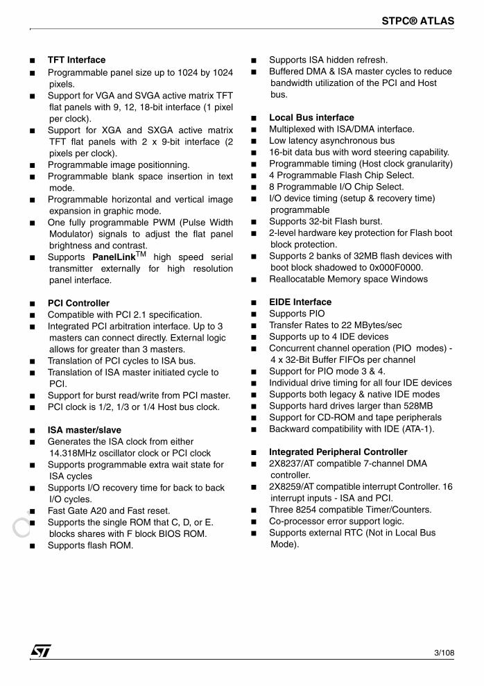
TFT Interface Programmable panel size up to 1024 by 1024
pixels. Support for VGA and SVGA active matrix TFT
flat panels with 9, 12, 18-bit interface (1 pixelper clock).
Support for XGA and SXGA active matrixTFT flat panels with 2 x 9-bit interface (2pixels per clock).
Programmable image positionning. Programmable blank space insertion in text
mode. Programmable horizontal and vertical image
expansion in graphic mode. One fully programmable PWM (Pulse Width
Modulator) signals to adjust the flat panelbrightness and contrast.
Supports PanelLinkTM high speed serialtransmitter externally for high resolutionpanel interface.
PCI Controller Compatible with PCI 2.1 specification. Integrated PCI arbitration interface. Up to 3
masters can connect directly. External logic allows for greater than 3 masters.
Translation of PCI cycles to ISA bus. Translation of ISA master initiated cycle to
PCI. Support for burst read/write from PCI master. PCI clock is 1/2, 1/3 or 1/4 Host bus clock.
ISA master/slave Generates the ISA clock from either
14.318MHz oscillator clock or PCI clock Supports programmable extra wait state for
ISA cycles Supports I/O recovery time for back to back
I/O cycles. Fast Gate A20 and Fast reset. Supports the single ROM that C, D, or E.
blocks shares with F block BIOS ROM. Supports flash ROM.
Supports ISA hidden refresh. Buffered DMA & ISA master cycles to reduce
bandwidth utilization of the PCI and Host bus.
Local Bus interface Multiplexed with ISA/DMA interface. Low latency asynchronous bus 16-bit data bus with word steering capability. Programmable timing (Host clock granularity) 4 Programmable Flash Chip Select. 8 Programmable I/O Chip Select. I/O device timing (setup & recovery time)
programmable Supports 32-bit Flash burst. 2-level hardware key protection for Flash boot
block protection. Supports 2 banks of 32MB flash devices with
boot block shadowed to 0x000F0000. Reallocatable Memory space Windows
EIDE Interface Supports PIO Transfer Rates to 22 MBytes/sec Supports up to 4 IDE devices Concurrent channel operation (PIO modes) -
4 x 32-Bit Buffer FIFOs per channel Support for PIO mode 3 & 4. Individual drive timing for all four IDE devices Supports both legacy & native IDE modes Supports hard drives larger than 528MB Support for CD-ROM and tape peripherals Backward compatibility with IDE (ATA-1).
Integrated Peripheral Controller 2X8237/AT compatible 7-channel DMA
controller. 2X8259/AT compatible interrupt Controller. 16
interrupt inputs - ISA and PCI. Three 8254 compatible Timer/Counters. Co-processor error support logic. Supports external RTC (Not in Local Bus
Mode).
Obsolete Product(
s) - O
bsolete Product(
s)
Obsolete Product(
s) - O
bsolete Product(
s)
STPC® ATLAS
4/108
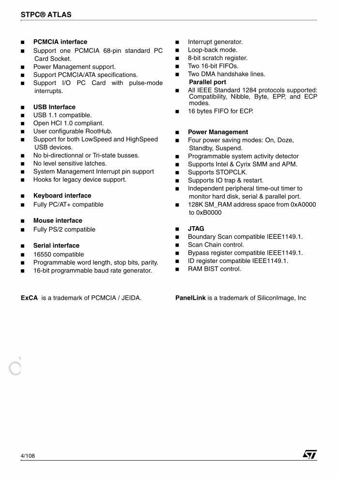
PCMCIA interface Support one PCMCIA 68-pin standard PC
Card Socket. Power Management support. Support PCMCIA/ATA specifications. Support I/O PC Card with pulse-mode
interrupts.
USB Interface USB 1.1 compatible. Open HCI 1.0 compliant. User configurable RootHub. Support for both LowSpeed and HighSpeed
USB devices. No bi-directionnal or Tri-state busses. No level sensitive latches. System Management Interrupt pin support Hooks for legacy device support.
Keyboard interface Fully PC/AT+ compatible
Mouse interface Fully PS/2 compatible
Serial interface 16550 compatible Programmable word length, stop bits, parity. 16-bit programmable baud rate generator.
Interrupt generator. Loop-back mode. 8-bit scratch register. Two 16-bit FIFOs. Two DMA handshake lines.
Parallel port All IEEE Standard 1284 protocols supported:
Compatibility, Nibble, Byte, EPP, and ECPmodes.
16 bytes FIFO for ECP.
Power Management Four power saving modes: On, Doze,
Standby, Suspend. Programmable system activity detector Supports Intel & Cyrix SMM and APM. Supports STOPCLK. Supports IO trap & restart. Independent peripheral time-out timer to
monitor hard disk, serial & parallel port. 128K SM_RAM address space from 0xA0000
to 0xB0000
JTAG Boundary Scan compatible IEEE1149.1. Scan Chain control. Bypass register compatible IEEE1149.1. ID register compatible IEEE1149.1. RAM BIST control.
ExCA is a trademark of PCMCIA / JEIDA. PanelLink is a trademark of SiliconImage, Inc
Obsolete Product(
s) - O
bsolete Product(
s)
Obsolete Product(
s) - O
bsolete Product(
s)
Table of Contents
108
5/108
1 GENERAL DESCRIPTION . . . . . . . . . . . . . . . . . . . . . . . . . . . . . . . . . . . . . . . . . . . . . . . . . . . . . . 81.1. ARCHITECTURE . . . . . . . . . . . . . . . . . . . . . . . . . . . . . . . . . . . . . . . . . . . . . . . . . . . . . . . . . 8
1.2. GRAPHICS FEATURES . . . . . . . . . . . . . . . . . . . . . . . . . . . . . . . . . . . . . . . . . . . . . . . . . . . 8
1.3. INTERFACES . . . . . . . . . . . . . . . . . . . . . . . . . . . . . . . . . . . . . . . . . . . . . . . . . . . . . . . . . . . 8
1.4. FEATURE MULTIPLEXING . . . . . . . . . . . . . . . . . . . . . . . . . . . . . . . . . . . . . . . . . . . . . . . . . 9
1.5. POWER MANAGEMENT . . . . . . . . . . . . . . . . . . . . . . . . . . . . . . . . . . . . . . . . . . . . . . . . . . . 9
1.6. JTAG . . . . . . . . . . . . . . . . . . . . . . . . . . . . . . . . . . . . . . . . . . . . . . . . . . . . . . . . . . . . . . . . . . 9
1.7. CLOCK TREE . . . . . . . . . . . . . . . . . . . . . . . . . . . . . . . . . . . . . . . . . . . . . . . . . . . . . . . . . . 11
2 PIN DESCRIPTION . . . . . . . . . . . . . . . . . . . . . . . . . . . . . . . . . . . . . . . . . . . . . . . . . . . . . . . . . . . 152.1. INTRODUCTION . . . . . . . . . . . . . . . . . . . . . . . . . . . . . . . . . . . . . . . . . . . . . . . . . . . . . . . . 15
2.2. SIGNAL DESCRIPTIONS . . . . . . . . . . . . . . . . . . . . . . . . . . . . . . . . . . . . . . . . . . . . . . . . . 21
2.2.1. BASIC CLOCKS AND RESETS . . . . . . . . . . . . . . . . . . . . . . . . . . . . . . . . . . . . . . . 212.2.2. MEMORY INTERFACE . . . . . . . . . . . . . . . . . . . . . . . . . . . . . . . . . . . . . . . . . . . . . 212.2.3. PCI INTERFACE . . . . . . . . . . . . . . . . . . . . . . . . . . . . . . . . . . . . . . . . . . . . . . . . . . 222.2.4. ISA BUS INTERFACE . . . . . . . . . . . . . . . . . . . . . . . . . . . . . . . . . . . . . . . . . . . . . . 222.2.5. PCMCIA INTERFACE . . . . . . . . . . . . . . . . . . . . . . . . . . . . . . . . . . . . . . . . . . . . . . 242.2.6. LOCAL BUS . . . . . . . . . . . . . . . . . . . . . . . . . . . . . . . . . . . . . . . . . . . . . . . . . . . . . . 252.2.7. IPC . . . . . . . . . . . . . . . . . . . . . . . . . . . . . . . . . . . . . . . . . . . . . . . . . . . . . . . . . . . . . 252.2.8. IDE INTERFACE . . . . . . . . . . . . . . . . . . . . . . . . . . . . . . . . . . . . . . . . . . . . . . . . . . 252.2.9. MONITOR INTERFACE . . . . . . . . . . . . . . . . . . . . . . . . . . . . . . . . . . . . . . . . . . . . . 252.2.10.VIDEO INTERFACE . . . . . . . . . . . . . . . . . . . . . . . . . . . . . . . . . . . . . . . . . . . . . . . . 262.2.11.TFT INTERFACE SIGNALS . . . . . . . . . . . . . . . . . . . . . . . . . . . . . . . . . . . . . . . . . . 262.2.12.USB Interface . . . . . . . . . . . . . . . . . . . . . . . . . . . . . . . . . . . . . . . . . . . . . . . . . . . . . 262.2.13.SERIAL INTERFACE . . . . . . . . . . . . . . . . . . . . . . . . . . . . . . . . . . . . . . . . . . . . . . . 262.2.14.KEYBOARD/MOUSE INTERFACE . . . . . . . . . . . . . . . . . . . . . . . . . . . . . . . . . . . . 272.2.15.PARALLEL PORT . . . . . . . . . . . . . . . . . . . . . . . . . . . . . . . . . . . . . . . . . . . . . . . . . . 272.2.16.MISCELLANEOUS . . . . . . . . . . . . . . . . . . . . . . . . . . . . . . . . . . . . . . . . . . . . . . . . . 272.2.17.COL_SEL Colour Select. JTAG Interface . . . . . . . . . . . . . . . . . . . . . . . . . . . . . . . . 27
2.3 SIGNAL DETAIL . . . . . . . . . . . . . . . . . . . . . . . . . . . . . . . . . . . . . . . . . . . . . . . . . . . . . . . . 27
3 STRAP OPTION . . . . . . . . . . . . . . . . . . . . . . . . . . . . . . . . . . . . . . . . . . . . . . . . . . . . . . . . . . . . . 363.1 STRAP OPTION REGISTER DESCRIPTION . . . . . . . . . . . . . . . . . . . . . . . . . . . . . . . . . . 38
3.1.1. STRAP REGISTER 0 . . . . . . . . . . . . . . . . . . . . . . . . . . . . . . . . . . . . . . . . . . . . . . . 383.1.2 STRAP REGISTER 1 . . . . . . . . . . . . . . . . . . . . . . . . . . . . . . . . . . . . . . . . . . . . . . . 393.1.3 HCLK PLL STRAP REGISTER . . . . . . . . . . . . . . . . . . . . . . . . . . . . . . . . . . . . . . . 403.1.4. STRAP REGISTER 2 . . . . . . . . . . . . . . . . . . . . . . . . . . . . . . . . . . . . . . . . . . . . . . . 413.1.5 CPUCLK/HCKL Deskew Programming . . . . . . . . . . . . . . . . . . . . . . . . . . . . . . . . . 42
3.2 TYPICAL STRAP OPTION IMPLEMENTATION . . . . . . . . . . . . . . . . . . . . . . . . . . . . . . . . 42
4 ELECTRICAL SPECIFICATIONS . . . . . . . . . . . . . . . . . . . . . . . . . . . . . . . . . . . . . . . . . . . . . . . . 444.1. INTRODUCTION . . . . . . . . . . . . . . . . . . . . . . . . . . . . . . . . . . . . . . . . . . . . . . . . . . . . . . . . 44
4.2. ELECTRICAL CONNECTIONS . . . . . . . . . . . . . . . . . . . . . . . . . . . . . . . . . . . . . . . . . . . . . 44
4.2.1. Power/Ground Connections/Decoupling . . . . . . . . . . . . . . . . . . . . . . . . . . . . . . . . . 444.2.2. Unused Input Pins . . . . . . . . . . . . . . . . . . . . . . . . . . . . . . . . . . . . . . . . . . . . . . . . . 444.2.3. Reserved Designated Pins . . . . . . . . . . . . . . . . . . . . . . . . . . . . . . . . . . . . . . . . . . . 44
4.3. ABSOLUTE MAXIMUM RATINGS . . . . . . . . . . . . . . . . . . . . . . . . . . . . . . . . . . . . . . . . . . . 44
4.3.1. 5V Tolerance . . . . . . . . . . . . . . . . . . . . . . . . . . . . . . . . . . . . . . . . . . . . . . . . . . . . . 444.4. DC CHARACTERISTICS . . . . . . . . . . . . . . . . . . . . . . . . . . . . . . . . . . . . . . . . . . . . . . . . . . 45
1
Obsolete Product(
s) - O
bsolete Product(
s)
Obsolete Product(
s) - O
bsolete Product(
s)
Table of Contents
6/108
4.5. AC CHARACTERISTICS . . . . . . . . . . . . . . . . . . . . . . . . . . . . . . . . . . . . . . . . . . . . . . . . . . 47
4.5.1. Power on sequence . . . . . . . . . . . . . . . . . . . . . . . . . . . . . . . . . . . . . . . . . . . . . . . . 484.5.2 RESET sequence . . . . . . . . . . . . . . . . . . . . . . . . . . . . . . . . . . . . . . . . . . . . . . . . . . 504.5.3. SDRAM interface . . . . . . . . . . . . . . . . . . . . . . . . . . . . . . . . . . . . . . . . . . . . . . . . . . 514.5.4 PCI interface . . . . . . . . . . . . . . . . . . . . . . . . . . . . . . . . . . . . . . . . . . . . . . . . . . . . . . 534.5.5 IPC interface . . . . . . . . . . . . . . . . . . . . . . . . . . . . . . . . . . . . . . . . . . . . . . . . . . . . . . 544.5.6 Isa interface AC Timing characteristics . . . . . . . . . . . . . . . . . . . . . . . . . . . . . . . . . 554.5.7. Local bus interface . . . . . . . . . . . . . . . . . . . . . . . . . . . . . . . . . . . . . . . . . . . . . . . . . 604.5.8 PCMCIA interface . . . . . . . . . . . . . . . . . . . . . . . . . . . . . . . . . . . . . . . . . . . . . . . . . . 634.5.9 IDE interface . . . . . . . . . . . . . . . . . . . . . . . . . . . . . . . . . . . . . . . . . . . . . . . . . . . . . . 644.5.10 TFT interface . . . . . . . . . . . . . . . . . . . . . . . . . . . . . . . . . . . . . . . . . . . . . . . . . . . . . 654.5.11 USB interface . . . . . . . . . . . . . . . . . . . . . . . . . . . . . . . . . . . . . . . . . . . . . . . . . . . . . 654.5.12 KEYBOARD & MOUSE INTERFACES . . . . . . . . . . . . . . . . . . . . . . . . . . . . . . . . . 654.5.13 IEEE1284 interface . . . . . . . . . . . . . . . . . . . . . . . . . . . . . . . . . . . . . . . . . . . . . . . . . 654.5.14 JTAG interface . . . . . . . . . . . . . . . . . . . . . . . . . . . . . . . . . . . . . . . . . . . . . . . . . . . . 66
5 MECHANICAL DATA . . . . . . . . . . . . . . . . . . . . . . . . . . . . . . . . . . . . . . . . . . . . . . . . . . . . . . . . . 675.1. 516-PIN PACKAGE DIMENSION . . . . . . . . . . . . . . . . . . . . . . . . . . . . . . . . . . . . . . . . . . . 67
5.2. 516-PIN PACKAGE THERMAL DATA . . . . . . . . . . . . . . . . . . . . . . . . . . . . . . . . . . . . . . . . 70
5.3. SOLDERING RECOMMENDATIONS . . . . . . . . . . . . . . . . . . . . . . . . . . . . . . . . . . . . . . . . 72
6 DESIGN GUIDELINES . . . . . . . . . . . . . . . . . . . . . . . . . . . . . . . . . . . . . . . . . . . . . . . . . . . . . . . . 736.1. TYPICAL APPLICATIONS . . . . . . . . . . . . . . . . . . . . . . . . . . . . . . . . . . . . . . . . . . . . . . . . . 73
6.1.1. Thin Client . . . . . . . . . . . . . . . . . . . . . . . . . . . . . . . . . . . . . . . . . . . . . . . . . . . . . . . . 736.1.2. Internet Terminal . . . . . . . . . . . . . . . . . . . . . . . . . . . . . . . . . . . . . . . . . . . . . . . . . . . 74
6.2. STPC CONFIGURATION . . . . . . . . . . . . . . . . . . . . . . . . . . . . . . . . . . . . . . . . . . . . . . . . . . 75
6.2.1. Local Bus / ISA bus . . . . . . . . . . . . . . . . . . . . . . . . . . . . . . . . . . . . . . . . . . . . . . . . 756.2.2. Clock configuration . . . . . . . . . . . . . . . . . . . . . . . . . . . . . . . . . . . . . . . . . . . . . . . . . 75
6.3. ARCHITECTURE RECOMMENDATIONS . . . . . . . . . . . . . . . . . . . . . . . . . . . . . . . . . . . . . 75
6.3.1. POWER DecouPling . . . . . . . . . . . . . . . . . . . . . . . . . . . . . . . . . . . . . . . . . . . . . . . . 766.3.2. 14MHz oscillator stage . . . . . . . . . . . . . . . . . . . . . . . . . . . . . . . . . . . . . . . . . . . . . . 766.3.3. SDRAM . . . . . . . . . . . . . . . . . . . . . . . . . . . . . . . . . . . . . . . . . . . . . . . . . . . . . . . . . . 776.3.4. PCI bus . . . . . . . . . . . . . . . . . . . . . . . . . . . . . . . . . . . . . . . . . . . . . . . . . . . . . . . . . . 806.3.5. Local Bus . . . . . . . . . . . . . . . . . . . . . . . . . . . . . . . . . . . . . . . . . . . . . . . . . . . . . . . . 816.3.6. IPC . . . . . . . . . . . . . . . . . . . . . . . . . . . . . . . . . . . . . . . . . . . . . . . . . . . . . . . . . . . . . 826.3.7. IDE / ISA dynamic demultiplexing . . . . . . . . . . . . . . . . . . . . . . . . . . . . . . . . . . . . . . 846.3.8. Basic audio using IDE interface . . . . . . . . . . . . . . . . . . . . . . . . . . . . . . . . . . . . . . . 846.3.9. VGA interface . . . . . . . . . . . . . . . . . . . . . . . . . . . . . . . . . . . . . . . . . . . . . . . . . . . . . 856.3.10.USB interface . . . . . . . . . . . . . . . . . . . . . . . . . . . . . . . . . . . . . . . . . . . . . . . . . . . . . 866.3.11.Keyboard/Mouse interface . . . . . . . . . . . . . . . . . . . . . . . . . . . . . . . . . . . . . . . . . . . 876.3.12.Parallel Port interface . . . . . . . . . . . . . . . . . . . . . . . . . . . . . . . . . . . . . . . . . . . . . . . 886.3.13. JTAG interface . . . . . . . . . . . . . . . . . . . . . . . . . . . . . . . . . . . . . . . . . . . . . . . . . . . . 89
6.4. PLACE AND ROUTE RECOMMENDATIONS . . . . . . . . . . . . . . . . . . . . . . . . . . . . . . . . . . 89
6.4.1. General recommendations . . . . . . . . . . . . . . . . . . . . . . . . . . . . . . . . . . . . . . . . . . . 896.4.2. PLL Definition and Implimentation . . . . . . . . . . . . . . . . . . . . . . . . . . . . . . . . . . . . . 896.4.3. Memory Interface . . . . . . . . . . . . . . . . . . . . . . . . . . . . . . . . . . . . . . . . . . . . . . . . . . 91
6.5. CLOCK TOPOLOGY FOR ON-BOARD SDRAM . . . . . . . . . . . . . . . . . . . . . . . . . . . . . . . . 93
6.5.1. PCI Interface . . . . . . . . . . . . . . . . . . . . . . . . . . . . . . . . . . . . . . . . . . . . . . . . . . . . . . 966.5.2. Thermal dissipation . . . . . . . . . . . . . . . . . . . . . . . . . . . . . . . . . . . . . . . . . . . . . . . . . 99
Obsolete Product(
s) - O
bsolete Product(
s)
Obsolete Product(
s) - O
bsolete Product(
s)
Table of Contents
7/108
6.6. DEBUG METHODOLOGY . . . . . . . . . . . . . . . . . . . . . . . . . . . . . . . . . . . . . . . . . . . . . . . . 103
6.6.1. Power Supplies . . . . . . . . . . . . . . . . . . . . . . . . . . . . . . . . . . . . . . . . . . . . . . . . . . . 1036.6.2. Boot sequence . . . . . . . . . . . . . . . . . . . . . . . . . . . . . . . . . . . . . . . . . . . . . . . . . . . 1036.6.3. ISA mode . . . . . . . . . . . . . . . . . . . . . . . . . . . . . . . . . . . . . . . . . . . . . . . . . . . . . . . 1036.6.4. Local Bus mode . . . . . . . . . . . . . . . . . . . . . . . . . . . . . . . . . . . . . . . . . . . . . . . . . . 1046.6.5. Summary . . . . . . . . . . . . . . . . . . . . . . . . . . . . . . . . . . . . . . . . . . . . . . . . . . . . . . . 1046.6.6. PCMCIA mode . . . . . . . . . . . . . . . . . . . . . . . . . . . . . . . . . . . . . . . . . . . . . . . . . . . 104
7 ORDERING DATA . . . . . . . . . . . . . . . . . . . . . . . . . . . . . . . . . . . . . . . . . . . . . . . . . . . . . . . . . . . 1087.1. ORDERING CODES . . . . . . . . . . . . . . . . . . . . . . . . . . . . . . . . . . . . . . . . . . . . . . . . . . . . 108
7.2 AVAILABLE PART NUMBERS . . . . . . . . . . . . . . . . . . . . . . . . . . . . . . . . . . . . . . . . . . . . 108
8 REVISION HISTORY . . . . . . . . . . . . . . . . . . . . . . . . . . . . . . . . . . . . . . . . . . . . . . . . . . . . . . . . . 109

Obsolete Product(
s) - O
bsolete Product(
s)
Obsolete Product(
s) - O
bsolete Product(
s)
STPC® ATLAS
8/108
1 GENERAL DESCRIPTION
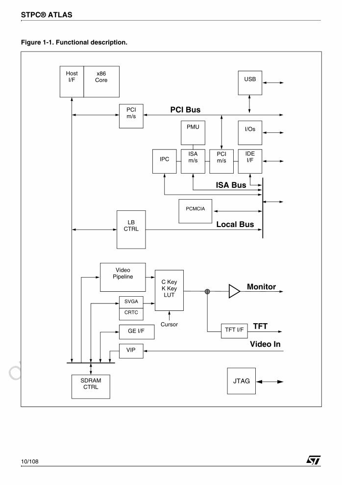
At the heart of the STPC Atlas is an advancedprocessor block that includes a powerful x86processor core along with a 64-bit SDRAMcontroller, advanced 64-bit accelerated graphicsand video controller, a high speed PCI buscontroller and industry standard PC chip setfunctions (Interrupt controller, DMA Controller,Interval timer and ISA bus).
The STPC Atlas has in addition, a TFT output, aVideo Input, an EIDE controller, a Local Businterface, PCMCIA and super I/O featuresincluding USB host hub.
1.1. ARCHITECTURE
The STPC Atlas makes use of a tightly coupledUnified Memory Architecture (UMA), where thesame memory array is used for CPU main memoryand graphics frame-buffer. This means a reductionin total system memory for system performancesthat are equal to that of a comparable frame bufferand system memory based system, and generallymuch better, due to the higher memory bandwidthallowed by attaching the graphics engine directlyto the 64-bit processor host interface running atthe speed of the processor bus rather than thetraditional PCI bus.
The 64-bit wide memory array provides the systemwith an 800MB/s peak bandwidth. This allows forhigher resolution screens and greater color depth.The processor bus runs at 133 MHz, furtherincreasing “standard” bandwidth by at least afactor of two.
The ‘standard’ PC chipset functions (DMA,interrupt controller, timers, power managementlogic) are integrated together with the x86processor core; additional low bandwidth functionssuch as communication ports are accessed by theSTPC Atlas via an internal ISA bus.
The PCI bus is the main data communication linkto the STPC Atlas chip. The STPC Atlas translatesappropriate host bus I/O and Memory cycles ontothe PCI bus. It also supports the generation ofConfiguration cycles on the PCI bus. The STPCAtlas, as a PCI bus agent (host bridge class), iscompatible with PCI specification 2.1. The chip-setalso implements the PCI mandatory headerregisters in Type 0 PCI configuration space foreasy porting of PCI aware system BIOS. Thedevice contains a PCI arbitration function for threeexternal PCI devices.
Figure 1-1 describes this architecture.
1.2. GRAPHICS FEATURES
Graphics functions are controlled through the on-chip SVGA controller and the monitor display isproduced through the 2D graphics display engine.
This Graphics Engine is tuned to work with thehost CPU to provide a balanced graphics systemwith a low silicon area cost. It performs limitedgraphics drawing operations which includehardware acceleration of text, bitblts, transparentblts and fills. The results of these operationschange the contents of the on-screen or off-screenframe buffer areas of SDRAM memory. The framebuffer can occupy a space up to 4 Mbytesanywhere in the physical main memory.
The maximum graphics resolution supported is1280 x 1024 in 16 Million colours at 75 Hz refreshrate and is VGA and SVGA compatible. Horizontaltiming fields are VGA compatible while the verticalfields are extended by one bit to accommodateabove display resolution.
To generate the TFT output, the STPC Atlasextracts the digital video stream before theRAMDAC and reformats it to the TFT format. Theheight and width of the flat panel areprogrammable.
1.3. INTERFACES
An industry standard EIDE (ATA 2) controller isbuilt in to the STPC Atlas and connected internallyvia the PCI bus.
The STPC Atlas integrates two USB ports.Universal Serial Bus (USB) is a general purposecommunications interface for connectingperipherals to a PC. The USB Open HostController Interface (Open HCI) Specification,revision 1.1, supports speeds of up to 12 MB/s.USB is royalty free and is likely to replace low-speed legacy serial, parallel, keyboard, mouseand floppy drive interfaces. USB Revision 1.1 isfully supported under Microsoft Windows 98 andWindows 2000.
The STPC Atlas PCMCIA controller has beenspecifically designed to provide the interface withPCMCIA cards which contain additional memoryor I/O
The power management control facilities includesocket power control, insertion/removal capability,power saving with Windows inactivity, NCScontrolled Chip Power Down, together with further
1
Obsolete Product(
s) - O
bsolete Product(
s)
Obsolete Product(
s) - O
bsolete Product(
s)
STPC® ATLAS
9/108
controls for 3.3V suspend with Modem RingResume Detection.
The STPC Atlas implements a multi-functionparallel port. The standard PC/AT compatiblelogical address assignments for LPT1, LPT2 andLPT3 are supported. It can be configured for anyof the following three modes and supports theIEEE Standard 1284 parallel interface protocolstandards, as follows:- Compatibility Mode (Forward channel, standard)- Nibble Mode (Reverse channel, PC compatible)- Byte Mode (Reverse channel, PS/2 compatible)
The General Purpose Input/Output (GPIO)interface provides a 16-bit I/O facility, using 16dedicated device pins. It is organised using twoblocks of 8-bit Registers, one for lines 0 to 7, theother for lines 8 to 15.Each GPIO port can be configured as an input oran output simply by programming the associatedport direction control register. All GPIO ports areconfigured as inputs at reset, which also latchesthe input levels into the Strap Registers. The inputstates of the ports are thus recorded automati-cally at reset, and this can be used as a strapregister anywhere in the system.
1.4. FEATURE MULTIPLEXING
The STPC Atlas BGA package has 516 balls. Thishowever is not sufficient for all of the integratedfunctions available; some features therefore sharethe same balls and cannot thus be used at thesame time. The STPC Atlas configuration is doneby ‘strap options’. This is a set of pull-up or pull-down resistors on the memory data bus, checkedon reset, which auto-configure the STPC Atlas.
There 3 multiplexed functions are the external ISAbus, the Local Bus and the PCMCIA interface.
1.5. POWER MANAGEMENT
The STPC Atlas core is compliant with theAdvanced Power Management (APM)specification to provide a standard method bywhich the BIOS can control the power used bypersonal computers. The Power Management Unit(PMU) module controls the power consumption,providing a comprehensive set of features thatcontrols the power usage and supportscompliance with the United States EnvironmentalProtection Agency's Energy Star ComputerProgram. The PMU provides the followinghardware structures to assist the software inmanaging the system power consumption:
- System Activity Detection.
- 3 power-down timers detecting system inactivity: - Doze timer (short durations). - Stand-by timer (medium durations). - Suspend timer (long durations).
- House-keeping activity detection.
- House-keeping timer to cope with short bursts ofhouse-keeping activity while dozing or in stand-bystate.
- Peripheral activity detection.
- Peripheral timer detecting peripheral inactivity
- SUSP# modulation to adjust the systemperformance in various power down states of thesystem including full power-on state.
- Power control outputs to disable power fromdifferent planes of the board.
Lack of system activity for progressively longerperiods of time is detected by the three powerdown timers. These timers can generate SMIinterrupts to CPU so that the SMM software canput the system in decreasing states of powerconsumption. Alternatively, system activity in apower down state can generate an SMI interrupt toallow the software to bring the system back up tofull power-on state. The chip-set supports up tothree power down states described above; thesecorrespond to decreasing levels of power savings.
Power down puts the STPC Atlas into suspendmode. The processor completes execution of thecurrent instruction, any pending decodedinstructions and associated bus cycles. During thesuspend mode, internal clocks are stopped.Removing power-down, the processor resumesinstruction fetching and begins execution in theinstruction stream at the point it had stopped.Because of the static nature of the core, nointernal data is lost.
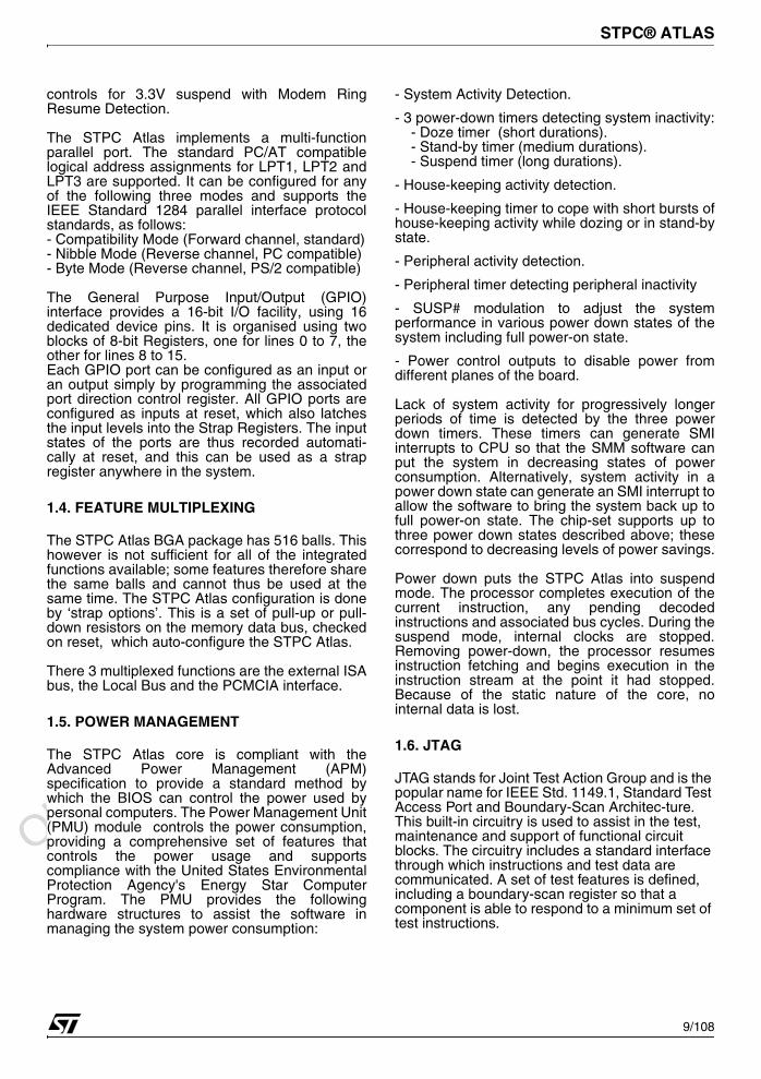
1.6. JTAG
JTAG stands for Joint Test Action Group and is the popular name for IEEE Std. 1149.1, Standard Test Access Port and Boundary-Scan Architec-ture. This built-in circuitry is used to assist in the test, maintenance and support of functional circuit blocks. The circuitry includes a standard interface through which instructions and test data are communicated. A set of test features is defined, including a boundary-scan register so that a component is able to respond to a minimum set of test instructions.
1
Obsolete Product(
s) - O
bsolete Product(
s)
Obsolete Product(
s) - O
bsolete Product(
s)
STPC® ATLAS
10/108
Figure 1-1. Functional description.
x86Core
HostI/F
SDRAMCTRL
SVGA
GE I/F
VIP
PCIm/s
LBCTRL
PCI Bus
ISAm/sIPC
PCIm/s
ISA Bus
CRTC
Cursor
Monitor
IDEI/F
PMU
VideoPipeline
C KeyK KeyLUT
Local Bus
PCMCIA
I/Os
USB
TFTTFT I/F
Video In
JTAG
1

Obsolete Product(
s) - O
bsolete Product(
s)
Obsolete Product(
s) - O
bsolete Product(
s)
STPC® ATLAS
11/108
1.7. CLOCK TREE
The STPC Atlas integrates many features andgenerates all its clocks from a single 14MHzoscillator. This results in multiple clock domains asdescribed in Figure 1-2.
The speed of the PLLs is either fixed (DEVCLK),either programmable by strap option (HCLK)either programmable by software (DCLK, MCLK).When in synchronized mode, MCLK speed is fixedto HCLKO speed and HCLKI is generated fromMCLKI.
Figure 1-2. STPC Atlas clock architecture
Kbd/Mouse
IPC
SDRAM controller
North Bridge
14.31818 MHz
XTALO XTALI
OSC14M ISACLK
1/4
DEVCLK
DEVCLK(24MHz)
PLL
(14MHz)
1/2
UARTs
HCLKPLL
PCICLKI PCICLKO
South Bridge
PWM1/21/3
HCLK
DCLKPLL
MCLKPLL
DCLKMCLKIMCLKO
USB
CRTC,Video,TFT
CPUx2
VCLK
48MHz
// Port
1/4
1/2
1/26
1/6
VIP
GE, LDE, AFE
PCMCIA
Local Bus
Host
ISAHCLKI
HCLKO
1
Obsolete Product(
s) - O
bsolete Product(
s)
Obsolete Product(
s) - O
bsolete Product(
s)
STPC® ATLAS
12/108
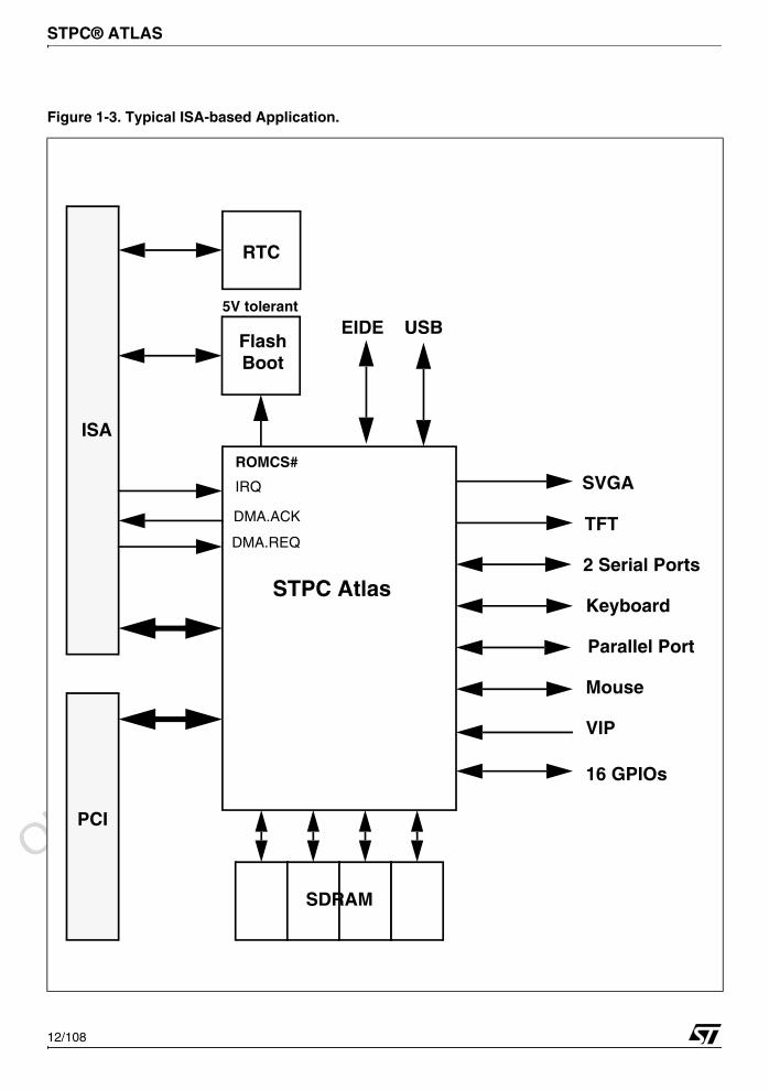
Figure 1-3. Typical ISA-based Application.
FlashBoot
ISA
PCI
EIDE
2 Serial Ports
Parallel Port
SVGA
TFT
IRQ
DMA.REQ
DMA.ACK
STPC Atlas
Mouse
Keyboard
USB
VIP
RTC
SDRAM
16 GPIOs
ROMCS#
5V tolerant
1
Obsolete Product(
s) - O
bsolete Product(
s)
Obsolete Product(
s) - O
bsolete Product(
s)
STPC® ATLAS
13/108
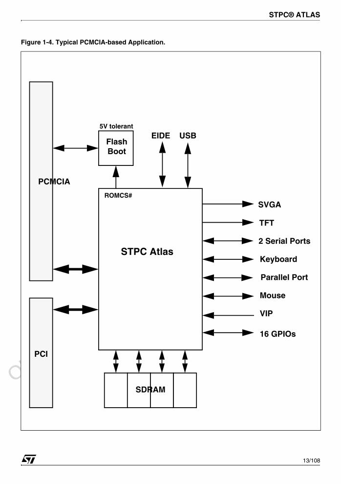
Figure 1-4. Typical PCMCIA-based Application.
PCI
FlashEIDE
2 Serial Ports
Parallel Port
SVGA
TFT
STPC Atlas
Mouse
Keyboard
USB
Boot
VIP
SDRAM
16 GPIOs
ROMCS#
PCMCIA
5V tolerant
1
Obsolete Product(
s) - O
bsolete Product(
s)
Obsolete Product(
s) - O
bsolete Product(
s)
STPC® ATLAS
14/108
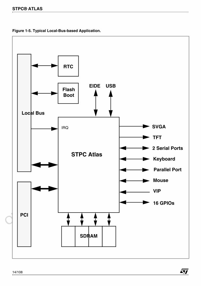
Figure 1-5. Typical Local-Bus-based Application.
FlashBoot
PCI
STPC Atlas
RTC
EIDE
2 Serial Ports
Parallel Port
SVGA
TFT
Mouse
Keyboard
USB
VIP
SDRAM
16 GPIOs
IRQ
Local Bus
1
Obsolete Product(
s) - O
bsolete Product(
s)
Obsolete Product(
s) - O
bsolete Product(
s)
STPC® ATLAS
15/108
2 PIN DESCRIPTION
2.1. INTRODUCTION
The STPC Atlas integrates most of thefunctionalities of the PC architecture. Therefore,many of the traditional interconnections betweenthe host PC microprocessor and the peripheraldevices are totally internal to the STPC Atlas. Thisoffers improved performance due to the tightcoupling of the processor core and it’s peripherals.As a result many of the external pin connectionsare made directly to the on-chip peripheralfunctions.
Table 2-1 describes the physical implementationlisting signal types and their functionalities. Table2-2 provides a full pin listing and description.
Table 2-6 provides a full listing of the STPC Atlaspackage pin location physical connection. Pleaserefer to the pin allocation drawing for reference.
Due to the number of pins available for thepackage, and the number of functional I/Os, somepins have several functions, selectable by strapoption on Reset. Table 2-4 provides a summary ofthese pins and their functions.
Non multi-functional pins associated with aparticular function are not available for useelsewhere when that function is disabled. For
example, when in the ISA mode, the Local Bus isdisabled totally and Local Bus pins are set to thetri-state (high-impedance) condition.
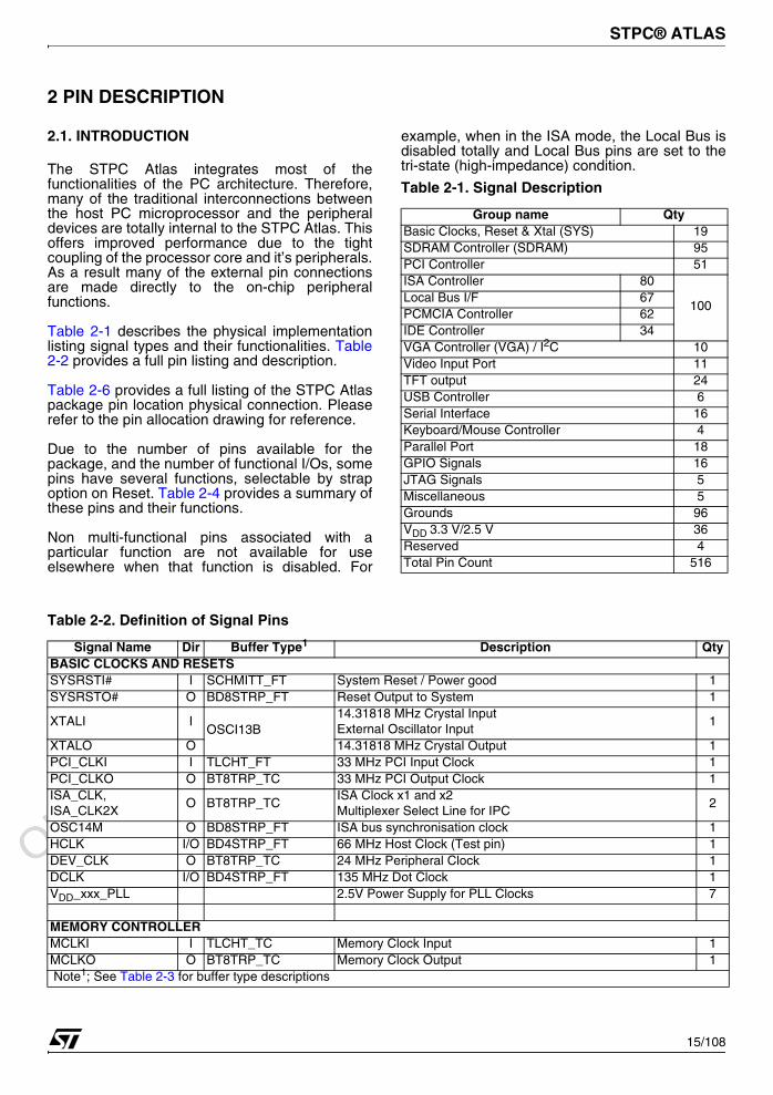
Table 2-1. Signal Description
Group name QtyBasic Clocks, Reset & Xtal (SYS) 19SDRAM Controller (SDRAM) 95PCI Controller 51ISA Controller 80
100Local Bus I/F 67PCMCIA Controller 62IDE Controller 34VGA Controller (VGA) / I2C 10Video Input Port 11TFT output 24USB Controller 6Serial Interface 16Keyboard/Mouse Controller 4Parallel Port 18GPIO Signals 16JTAG Signals 5Miscellaneous 5Grounds 96VDD 3.3 V/2.5 V 36Reserved 4Total Pin Count 516
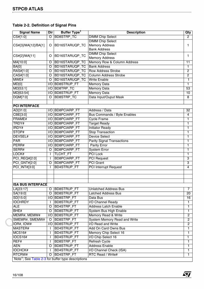
Table 2-2. Definition of Signal Pins
Signal Name Dir Buffer Type1 Description QtyBASIC CLOCKS AND RESETSSYSRSTI# I SCHMITT_FT System Reset / Power good 1SYSRSTO# O BD8STRP_FT Reset Output to System 1
XTALI IOSCI13B
14.31818 MHz Crystal InputExternal Oscillator Input
1
XTALO O 14.31818 MHz Crystal Output 1PCI_CLKI I TLCHT_FT 33 MHz PCI Input Clock 1PCI_CLKO O BT8TRP_TC 33 MHz PCI Output Clock 1ISA_CLK, ISA_CLK2X
O BT8TRP_TCISA Clock x1 and x2Multiplexer Select Line for IPC
2
OSC14M O BD8STRP_FT ISA bus synchronisation clock 1 HCLK I/O BD4STRP_FT 66 MHz Host Clock (Test pin) 1DEV_CLK O BT8TRP_TC 24 MHz Peripheral Clock 1DCLK I/O BD4STRP_FT 135 MHz Dot Clock 1VDD_xxx_PLL 2.5V Power Supply for PLL Clocks 7
MEMORY CONTROLLERMCLKI I TLCHT_TC Memory Clock Input 1MCLKO O BT8TRP_TC Memory Clock Output 1Note1; See Table 2-3 for buffer type descriptions
1
Obsolete Product(
s) - O
bsolete Product(
s)
Obsolete Product(
s) - O
bsolete Product(
s)
STPC® ATLAS
16/108
CS#[1:0] O BD8STRP_TC DIMM Chip Select 2
CS#[3]/MA[12]/BA[1] O BD16STARUQP_TCDIMM Chip SelectMemory AddressBank Address
1
CS#[2]/MA[11] O BD16STARUQP_TCDIMM Chip SelectMemory Address
1
MA[10:0] O BD16STARUQP_TC Memory Row & Column Address 11BA[0] O BD16STARUQP_TC Bank Address 1RAS#[1:0] O BD16STARUQP_TC Row Address Strobe 2CAS#[1:0] O BD16STARUQP_TC Column Address Strobe 2MWE# O BD16STARUQP_TC Write Enable 1MD[0] I/O BD8STRUP_FT Memory Data 1MD[53:1] I/O BD8TRP_TC Memory Data 53MD[63:54] I/O BD8STRUP_FT Memory Data 10DQM[7:0] O BD8STRP_TC Data Input/Ouput Mask 8
PCI INTERFACEAD[31:0] I/O BD8PCIARP_FT Address / Data 32CBE[3:0] I/O BD8PCIARP_FT Bus Commands / Byte Enables 4FRAME# I/O BD8PCIARP_FT Cycle Frame 1TRDY# I/O BD8PCIARP_FT Target Ready 1IRDY# I/O BD8PCIARP_FT Initiator Ready 1STOP# I/O BD8PCIARP_FT Stop Transaction 1DEVSEL# I/O BD8PCIARP_FT Device Select 1PAR I/O BD8PCIARP_FT Parity Signal Transactions 1PERR# I/O BD8PCIARP_FT Parity Error 1SERR# O BD8PCIARP_FT System Error 1LOCK# I TLCHT_FT PCI Lock 1PCI_REQ#[2:0] I BD8PCIARP_FT PCI Request 3PCI_GNT#[2:0] O BD8PCIARP_FT PCI Grant 3PCI_INT#[3:0] I BD4STRUP_FT PCI Interrupt Request 4
ISA BUS INTERFACELA[23:17] O BD8STRUP_FT Unlatched Address Bus 7SA[19:0] O BD8STRUP_FT Latched Address Bus 20SD[15:0] I/O BD8STRP_FT Data Bus 16IOCHRDY I BD8STRUP_FT I/O Channel Ready 1ALE O BD4STRP_FT Address Latch Enable 1BHE# O BD8STRUP_FT System Bus High Enable 1MEMR#, MEMW# I/O BD8STRUP_FT Memory Read & Write 2SMEMR#, SMEMW# O BD8STRP_FT System Memory Read and Write 2IOR#, IOW# I/O BD8STRUP_FT I/O Read and Write 2MASTER# I BD4STRUP_FT Add On Card Owns Bus 1MCS16# I BD4STRUP_FT Memory Chip Select 16 1IOCS16# I BD4STRUP_FT I/O Chip Select 16 1REF# I BD8STRP_FT Refresh Cycle 1AEN O BD8STRUP_FT Address Enable 1IOCHCK# I BD4STRUP_FT I/O Channel Check (ISA) 1RTCRW# O BD4STRP_FT RTC Read / Write# 1
Table 2-2. Definition of Signal Pins
Signal Name Dir Buffer Type1 Description Qty
Note1; See Table 2-3 for buffer type descriptions
1

Obsolete Product(
s) - O
bsolete Product(
s)
Obsolete Product(
s) - O
bsolete Product(
s)
STPC® ATLAS
17/108
RTCDS# O BD4STRP_FT RTC Data Strobe 1RTCAS O BD4STRP_FT RTC Address Strobe 1RMRTCCS# O BD4STRP_FT ROM / RTC Chip Select 1GPIOCS# I/O BD4STRP_FT General Purpose Chip Select 1IRQ_MUX[3:0] I BD4STRP_FT Multiplexed Interrupt Request 4DACK_ENC[2:0] O BD4STRP_FT DMA Acknowledge 3DREQ_MUX[1:0] I BD4STRP_FT Multiplexed DMA Request 2TC O BD4STRP_FT ISA Terminal Count 1ISAOE# I BD4STRP_FT ISA (0) / IDE (1) SELECTION 1KBCS# I/O BD4STRP_FT External Keyboard CHIP SELECT 1ZWS# I BD4STRP_FT ZERO WAIT STATE 1
PCMCIA INTERFACERESET O BD8STRP_FT Reset 1A[23:0] O BD8STRUP_FT Address Bus 24D[15:0] I/O BD8STRP_FT Data Bus 16IORD#, IOWR# O BD8STRUP_FT I/O Read and Write 2
WP / IOIS16# I BD4STRUP_FTDMA Request // Write ProtectI/O Size is 16 bit
1
BVD2, BVD1 I BD4STRUP_FT Battery Voltage Detect 2READY# / IREQ# I BD4STRUP_FT Busy / Ready# // Interrupt Request 1WAIT# I BD8STRUP_FT Wait 1OE# O BD8STRUP_FT Output Enable // DMA Terminal Count 1WE# O BD4STRP_FT Write Enable // DMA Terminal Count 1REG# O BD4STRUP_FT DMA Acknowledge // Register 1CD2#, CD1# I BD4STRUP_FT Card Detect 2CE2#, CE1# O BD4STRP_FT Card Enable 2VCC5_EN O BD4STRP_FT Power Switch control: 5 V power 1VCC3_EN O BD8STRP_FT Power Switch control: 3.3 V power 1VPP_PGM O BD8STRP_FT Power Switch control: Program power 1VPP_VCC O BD4STRP_FT Power Switch control: VCC power 1GPI# I BD4STRP_FT General Purpose Input 1
LOCAL BUS INTERFACEPA[24:20,15,9:8,3:0] O BD4STRP_FT Address Bus [24:20], [15], [9:8], [3:0] 12PA[19,11] O BD8STRP_FT Address Bus [19], [11] 2PA[18:16,14:12,7:4] O BD8STRUP_FT Address Bus [18:16], [14:12], [7:4] 10PA[10] O BD4STRUP_FT Address Bus [10] 1PD[15:0] I/O BD8STRP_FT Data Bus [15:0] 16PRD# O BD4STRUP_FT Memory and I/O Read signal 1PWR# O BD4STRUP_FT Memory and I/O Write signal 1PRDY I BD8STRUP_FT Data Ready 1IOCS#[7:4] O BD4STRUP_FT I/O Chip Select 4IOCS#[3] O BD4STRP_FT I/O Chip Select 1IOCS#[2:0] O BD8STRUP_FT I/O Chip Select 3PBE#[1] O BD8STRP_FT Upper Byte Enable (PD[15:8]) 1PBE#[0] O BD4STRUP_FT Lower Byte Enable (PD[7:0]) 1FCS0# O BD4STRP_FT Flash Bank 0 Chip Select 1FCS1# O BT8TRP_TC Flash Bank 1 Chip Select 1
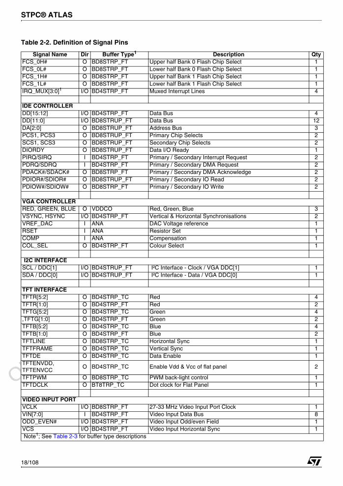
Table 2-2. Definition of Signal Pins
Signal Name Dir Buffer Type1 Description Qty
Note1; See Table 2-3 for buffer type descriptions
1
Obsolete Product(
s) - O
bsolete Product(
s)
Obsolete Product(
s) - O
bsolete Product(
s)
STPC® ATLAS
18/108
FCS_0H# O BD8STRP_FT Upper half Bank 0 Flash Chip Select 1FCS_0L# O BD8STRP_FT Lower half Bank 0 Flash Chip Select 1FCS_1H# O BD8STRP_FT Upper half Bank 1 Flash Chip Select 1FCS_1L# O BD8STRP_FT Lower half Bank 1 Flash Chip Select 1IRQ_MUX[3:0]1 I/O BD4STRP_FT Muxed Interrupt Lines 4
IDE CONTROLLERDD[15:12] I/O BD4STRP_FT Data Bus 4DD[11:0] I/O BD8STRUP_FT Data Bus 12DA[2:0] O BD8STRUP_FT Address Bus 3PCS1, PCS3 O BD8STRUP_FT Primary Chip Selects 2SCS1, SCS3 O BD8STRUP_FT Secondary Chip Selects 2DIORDY O BD8STRUP_FT Data I/O Ready 1PIRQ/SIRQ I BD4STRP_FT Primary / Secondary Interrupt Request 2PDRQ/SDRQ I BD4STRP_FT Primary / Secondary DMA Request 2 PDACK#/SDACK# O BD8STRP_FT Primary / Secondary DMA Acknowledge 2PDIOR#/SDIOR# O BD8STRUP_FT Primary / Secondary IO Read 2PDIOW#/SDIOW# O BD8STRP_FT Primary / Secondary IO Write 2
VGA CONTROLLERRED, GREEN, BLUE O VDDCO Red, Green, Blue 3VSYNC, HSYNC I/O BD4STRP_FT Vertical & Horizontal Synchronisations 2VREF_DAC I ANA DAC Voltage reference 1RSET I ANA Resistor Set 1COMP I ANA Compensation 1COL_SEL O BD4STRP_FT Colour Select 1
I2C INTERFACESCL / DDC[1] I/O BD4STRUP_FT I²C Interface - Clock / VGA DDC[1] 1SDA / DDC[0] I/O BD4STRUP_FT I²C Interface - Data / VGA DDC[0] 1
TFT INTERFACE TFTR[5:2] O BD4STRP_TC Red 4TFTR[1:0] O BD4STRP_FT Red 2TFTG[5:2] O BD4STRP_TC Green 4,TFTG[1:0] O BD4STRP_FT Green 2TFTB[5:2] O BD4STRP_TC Blue 4TFTB[1:0] O BD4STRP_FT Blue 2TFTLINE O BD8STRP_TC Horizontal Sync 1TFTFRAME O BD4STRP_TC Vertical Sync 1TFTDE O BD4STRP_TC Data Enable 1TFTENVDD, TFTENVCC
O BD4STRP_TC Enable Vdd & Vcc of flat panel 2
TFTPWM O BD8STRP_TC PWM back-light control 1TFTDCLK O BT8TRP_TC Dot clock for Flat Panel 1
VIDEO INPUT PORTVCLK I/O BD8STRP_FT 27-33 MHz Video Input Port Clock 1VIN[7:0] I BD4STRP_FT Video Input Data Bus 8ODD_EVEN# I/O BD4STRP_FT Video Input Odd/even Field 1VCS I/O BD4STRP_FT Video Input Horizontal Sync 1
Table 2-2. Definition of Signal Pins
Signal Name Dir Buffer Type1 Description Qty
Note1; See Table 2-3 for buffer type descriptions
1
Obsolete Product(
s) - O
bsolete Product(
s)
Obsolete Product(
s) - O
bsolete Product(
s)
STPC® ATLAS
19/108
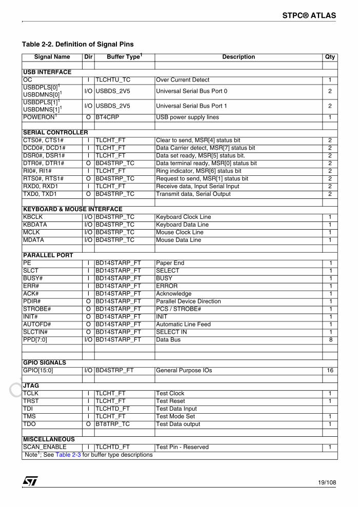
USB INTERFACEOC I TLCHTU_TC Over Current Detect 1USBDPLS[0]1 USBDMNS[0]1
I/O USBDS_2V5 Universal Serial Bus Port 0 2
USBDPLS[1]1
USBDMNS[1]1I/O USBDS_2V5 Universal Serial Bus Port 1 2
POWERON1 O BT4CRP USB power supply lines 1
SERIAL CONTROLLERCTS0#, CTS1# I TLCHT_FT Clear to send, MSR[4] status bit 2DCD0#, DCD1# I TLCHT_FT Data Carrier detect, MSR[7] status bit 2DSR0#, DSR1# I TLCHT_FT Data set ready, MSR[5] status bit. 2DTR0#, DTR1# O BD4STRP_TC Data terminal ready, MSR[0] status bit 2RI0#, RI1# I TLCHT_FT Ring indicator, MSR[6] status bit 2RTS0#, RTS1# O BD4STRP_TC Request to send, MSR[1] status bit 2RXD0, RXD1 I TLCHT_FT Receive data, Input Serial Input 2TXD0, TXD1 O BD4STRP_TC Transmit data, Serial Output 2
KEYBOARD & MOUSE INTERFACEKBCLK I/O BD4STRP_TC Keyboard Clock Line 1KBDATA I/O BD4STRP_TC Keyboard Data Line 1MCLK I/O BD4STRP_TC Mouse Clock Line 1MDATA I/O BD4STRP_TC Mouse Data Line 1
PARALLEL PORT PE I BD14STARP_FT Paper End 1SLCT I BD14STARP_FT SELECT 1BUSY# I BD14STARP_FT BUSY 1ERR# I BD14STARP_FT ERROR 1ACK# I BD14STARP_FT Acknowledge 1PDIR# O BD14STARP_FT Parallel Device Direction 1STROBE# O BD14STARP_FT PCS / STROBE# 1INIT# O BD14STARP_FT INIT 1AUTOFD# O BD14STARP_FT Automatic Line Feed 1SLCTIN# O BD14STARP_FT SELECT IN 1PPD[7:0] I/O BD14STARP_FT Data Bus 8
GPIO SIGNALSGPIO[15:0] I/O BD4STRP_FT General Purpose IOs 16
JTAG TCLK I TLCHT_FT Test Clock 1TRST I TLCHT_FT Test Reset 1TDI I TLCHTD_FT Test Data InputTMS I TLCHT_FT Test Mode Set 1TDO O BT8TRP_TC Test Data output 1
MISCELLANEOUSSCAN_ENABLE I TLCHTD_FT Test Pin - Reserved 1
Table 2-2. Definition of Signal Pins
Signal Name Dir Buffer Type1 Description Qty
Note1; See Table 2-3 for buffer type descriptions
1
Obsolete Product(
s) - O
bsolete Product(
s)
Obsolete Product(
s) - O
bsolete Product(
s)
STPC® ATLAS
20/108
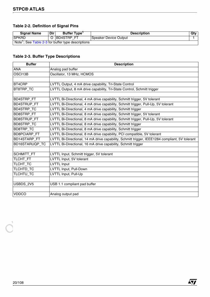
SPKRD O BD4STRP_FT Speaker Device Output 1
Table 2-2. Definition of Signal Pins
Signal Name Dir Buffer Type1 Description Qty
Note1; See Table 2-3 for buffer type descriptions
Table 2-3. Buffer Type Descriptions
Buffer DescriptionANA Analog pad bufferOSCI13B Oscillator, 13 MHz, HCMOS
BT4CRP LVTTL Output, 4 mA drive capability, Tri-State ControlBT8TRP_TC LVTTL Output, 8 mA drive capability, Tri-State Control, Schmitt trigger
BD4STRP_FT LVTTL Bi-Directional, 4 mA drive capability, Schmitt trigger, 5V tolerantBD4STRUP_FT LVTTL Bi-Directional, 4 mA drive capability, Schmitt trigger, Pull-Up, 5V tolerantBD4STRP_TC LVTTL Bi-Directional, 4 mA drive capability, Schmitt triggerBD8STRP_FT LVTTL Bi-Directional, 8 mA drive capability, Schmitt trigger, 5V tolerantBD8STRUP_FT LVTTL Bi-Directional, 8 mA drive capability, Schmitt trigger, Pull-Up, 5V tolerantBD8STRP_TC LVTTL Bi-Directional, 8 mA drive capability, Schmitt triggerBD8TRP_TC LVTTL Bi-Directional, 8 mA drive capability, Schmitt triggerBD8PCIARP_FT LVTTL Bi-Directional, 8 mA drive capability, PCI compatible, 5V tolerantBD14STARP_FT LVTTL Bi-Directional, 14 mA drive capability, Schmitt trigger, IEEE1284 compliant, 5V tolerantBD16STARUQP_TC LVTTL Bi-Directional, 16 mA drive capability, Schmitt trigger
SCHMITT_FT LVTTL Input, Schmitt trigger, 5V tolerantTLCHT_FT LVTTL Input, 5V tolerantTLCHT_TC LVTTL InputTLCHTD_TC LVTTL Input, Pull-DownTLCHTU_TC LVTTL Input, Pull-Up
USBDS_2V5 USB 1.1 compliant pad buffer
VDDCO Analog output pad
1

Obsolete Product(
s) - O
bsolete Product(
s)
Obsolete Product(
s) - O
bsolete Product(
s)
STPC® ATLAS
21/108
2.2. SIGNAL DESCRIPTIONS
2.2.1. BASIC CLOCKS AND RESETS
SYSRSTI# System Reset/Power good. This inputis low when the reset switch is depressed.Otherwise, it reflects the power supply’s powergood signal. PWGD is asynchronous to all clocks,and acts as a negative active reset. The resetcircuit initiates a hard reset on the rising edge ofPWGD.
Note that while Reset is being asserted, thesignals on the device pins are in an unknownstate.
SYSRSTO# Reset Output to System. This is thesystem reset signal and is used to reset the rest ofthe components (not on Host bus) in the system.The ISA bus reset is an externally invertedbuffered version of this output and the PCI busreset is an externally buffered version of thisoutput.
XTALI 14.3 MHz Crystal InputXTALO 14.3 MHz Crystal Output. These pins areprovided for the connection of an external 14.318MHz crystal to provide the reference clock for theinternal frequency synthesizer, from which theHCLK and CLK24M signals are generated.
PCI_CLKI 33 MHz PCI Input Clock. This signalmust be connected to a clock generator and isusually connected to PCI_CLKO.
PCI_CLKO 33 MHz PCI Output Clock. This is themaster PCI bus clock output.
ISA_CLK ISA Clock Output (also MultiplexerSelect Line For IPC). This pin produces the Clocksignal for the ISA bus. It is also used withISA_CLK2X as the multiplexer control lines for theInterrupt Controller Interrupt input lines. This is adivided down version of the PCICLK or OSC14M.
ISA_CLKX2 ISA Clock Output (also MultiplexerSelect Line For IPC). This pin produces a signal attwice the frequency of the ISA bus Clock signal. Itis also used with ISA_CLK as the multiplexercontrol lines for the Interrupt Controller Interruptinput lines.
CLK14M ISA bus synchronisation clock. This isthe buffered 14.318 MHz clock to the ISA bus.
HCLK Host Clock. This is the host clock. Itsfrequency can vary from 25 to 66 MHz. All hosttransactions and PCI transactions aresynchronized to this clock. Host transactionsexecuted by the DRAM controller are also drivenby this clock.
DEV_CLK 24 MHz Peripheral Clock (floppy drive).This 24 MHz signal is provided as a conveniencefor the system integration of a Floppy Disk driverfunction in an external chip. This clock signal is notavailable in Local Bus mode.
DCLK 135 MHz Dot Clock. This is the dot clock,which drives graphics display cycles. Its frequencycan be as high as 135 MHz, and it is required tohave a worst case duty cycle of 60-40. For furtherdetails, refer to Section 3.1.4. bit 4.
2.2.2. MEMORY INTERFACE
MCLKI Memory Clock Input. This clock is drivingthe SDRAM controller, the graphics engine anddisplay controller. This input should be a bufferedversion of the MCLKO signal with the track lengthsbetween the buffer and the pin matched with thetrack lengths between the buffer and the MemoryBanks.
MCLKO Memory Clock Output. This clock drivesthe Memory Banks on board and is generatedfrom an internal PLL.
The STPC Atlas MClock signal can run up to100MHz reliably, but PCB layout is so critical thatthe maximum guaranteed speed is 90MHz
CS#[1:0] Chip Select These signals are used todisable or enable device operation by masking orenabling all SDRAM inputs except MCLK, CKE,and DQM.
CS#[2]/MA[11] Chip Select/Bank Address Thispin is CS#[2] in the case when 16-Mbit devices areused. For all other densities, it becomes MA[11].
CS#[3]/MA[12]/BA[1] Chip Select/ MemoryAddress/ Bank Address This pin is CS#[3] in thecase when 16 Mbit devices are used. For all otherdensities, it becomes MA[12] when 2 internalbanks devices are used and BA[1] when 4 internalbank devices are used.
MA[10:0] Memory Address. Multiplexed row andcolumn address lines.
BA[0] Bank Address. Internal bank address line.
MD[63:0] Memory Data. This is the 64-bit memorydata bus. This bus is also used as input at therising edge of SYSRSTI# to latch in power-upconfiguration information into the ADPC strapregisters.
RAS#[1:0] Row Address Strobe. There are twoactive-low row address strobe output signals. TheRAS# signals drive the memory devices directlywithout any external buffering.
1
Obsolete Product(
s) - O
bsolete Product(
s)
Obsolete Product(
s) - O
bsolete Product(
s)
STPC® ATLAS
22/108
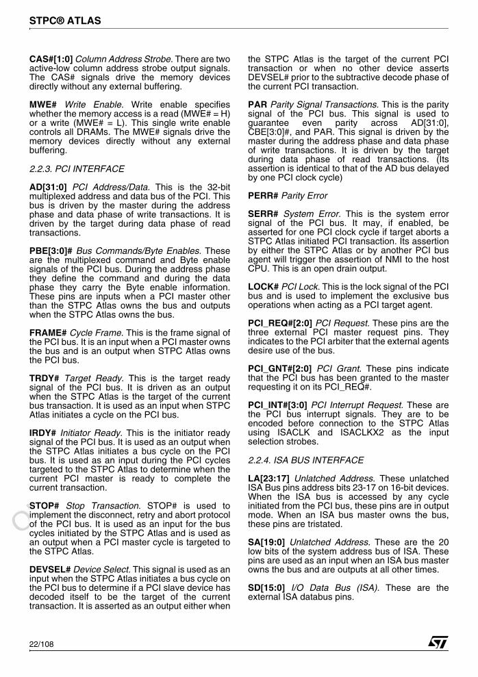
CAS#[1:0] Column Address Strobe. There are twoactive-low column address strobe output signals.The CAS# signals drive the memory devicesdirectly without any external buffering.
MWE# Write Enable. Write enable specifieswhether the memory access is a read (MWE# = H)or a write (MWE# = L). This single write enablecontrols all DRAMs. The MWE# signals drive thememory devices directly without any externalbuffering.
2.2.3. PCI INTERFACE
AD[31:0] PCI Address/Data. This is the 32-bitmultiplexed address and data bus of the PCI. Thisbus is driven by the master during the addressphase and data phase of write transactions. It isdriven by the target during data phase of readtransactions.
PBE[3:0]# Bus Commands/Byte Enables. Theseare the multiplexed command and Byte enablesignals of the PCI bus. During the address phasethey define the command and during the dataphase they carry the Byte enable information.These pins are inputs when a PCI master otherthan the STPC Atlas owns the bus and outputswhen the STPC Atlas owns the bus.
FRAME# Cycle Frame. This is the frame signal ofthe PCI bus. It is an input when a PCI master ownsthe bus and is an output when STPC Atlas ownsthe PCI bus.
TRDY# Target Ready. This is the target readysignal of the PCI bus. It is driven as an outputwhen the STPC Atlas is the target of the currentbus transaction. It is used as an input when STPCAtlas initiates a cycle on the PCI bus.
IRDY# Initiator Ready. This is the initiator readysignal of the PCI bus. It is used as an output whenthe STPC Atlas initiates a bus cycle on the PCIbus. It is used as an input during the PCI cyclestargeted to the STPC Atlas to determine when thecurrent PCI master is ready to complete thecurrent transaction.
STOP# Stop Transaction. STOP# is used toimplement the disconnect, retry and abort protocolof the PCI bus. It is used as an input for the buscycles initiated by the STPC Atlas and is used asan output when a PCI master cycle is targeted tothe STPC Atlas.
DEVSEL# Device Select. This signal is used as aninput when the STPC Atlas initiates a bus cycle onthe PCI bus to determine if a PCI slave device hasdecoded itself to be the target of the currenttransaction. It is asserted as an output either when
the STPC Atlas is the target of the current PCItransaction or when no other device assertsDEVSEL# prior to the subtractive decode phase ofthe current PCI transaction.
PAR Parity Signal Transactions. This is the paritysignal of the PCI bus. This signal is used toguarantee even parity across AD[31:0],CBE[3:0]#, and PAR. This signal is driven by themaster during the address phase and data phaseof write transactions. It is driven by the targetduring data phase of read transactions. (Itsassertion is identical to that of the AD bus delayedby one PCI clock cycle)
PERR# Parity Error
SERR# System Error. This is the system errorsignal of the PCI bus. It may, if enabled, beasserted for one PCI clock cycle if target aborts aSTPC Atlas initiated PCI transaction. Its assertionby either the STPC Atlas or by another PCI busagent will trigger the assertion of NMI to the hostCPU. This is an open drain output.
LOCK# PCI Lock. This is the lock signal of the PCIbus and is used to implement the exclusive busoperations when acting as a PCI target agent.
PCI_REQ#[2:0] PCI Request. These pins are thethree external PCI master request pins. Theyindicates to the PCI arbiter that the external agentsdesire use of the bus.
PCI_GNT#[2:0] PCI Grant. These pins indicatethat the PCI bus has been granted to the masterrequesting it on its PCI_REQ#.
PCI_INT#[3:0] PCI Interrupt Request. These arethe PCI bus interrupt signals. They are to beencoded before connection to the STPC Atlasusing ISACLK and ISACLKX2 as the inputselection strobes.
2.2.4. ISA BUS INTERFACE
LA[23:17] Unlatched Address. These unlatchedISA Bus pins address bits 23-17 on 16-bit devices.When the ISA bus is accessed by any cycleinitiated from the PCI bus, these pins are in outputmode. When an ISA bus master owns the bus,these pins are tristated.
SA[19:0] Unlatched Address. These are the 20low bits of the system address bus of ISA. Thesepins are used as an input when an ISA bus masterowns the bus and are outputs at all other times.
SD[15:0] I/O Data Bus (ISA). These are theexternal ISA databus pins.
1

Obsolete Product(
s) - O
bsolete Product(
s)
Obsolete Product(
s) - O
bsolete Product(
s)
STPC® ATLAS
23/108
IOCHRDY IO Channel Ready. IOCHRDY is the IOchannel ready signal of the ISA bus and is drivenas an output in response to an ISA master cycletargeted to the host bus or an internal register ofthe STPC Atlas. The STPC Atlas monitors thissignal as an input when performing an ISA cycleon behalf of the host CPU, DMA master or refresh.ISA masters which do not monitor IOCHRDY arenot guaranteed to work with the STPC Atlas sincethe access to the system memory can beconsiderably delayed due to CRT refresh or awrite back cycle.
ALE Address Latch Enable. This is the addresslatch enable output of the ISA bus and is assertedby the STPC Atlas to indicate that LA23-17, SA19-0, AEN and SBHE# signals are valid. The ALE isdriven high during refresh, DMA master or an ISAmaster cycles by the STPC Atlas.ALE is driven low after reset.
BHE# System Bus High Enable. This signal, whenasserted, indicates that a data Byte is beingtransferred on SD15-8 lines. It is used as an inputwhen an ISA master owns the bus and is an outputat all other times.
MEMR# Memory Read. This is the memory readcommand signal of the ISA bus. It is used as aninput when an ISA master owns the bus and is anoutput at all other times.The MEMR# signal is active during refresh.
MEMW# Memory Write. This is the memory writecommand signal of the ISA bus. It is used as aninput when an ISA master owns the bus and is anoutput at all other times.
SMEMR# System Memory Read. The STPC Atlasgenerates SMEMR# signal of the ISA bus onlywhen the address is below one MByte or the cycleis a refresh cycle.
SMEMW# System Memory Write. The STPC Atlasgenerates SMEMW# signal of the ISA bus onlywhen the address is below one MByte.
IOR# I/O Read. This is the IO read commandsignal of the ISA bus. It is an input when an ISAmaster owns the bus and is an output at all othertimes.
IOW# I/O Write. This is the IO write commandsignal of the ISA bus. It is an input when an ISAmaster owns the bus and is an output at all othertimes.
MASTER# Add On Card Owns Bus. This signal isactive when an ISA device has been granted busownership.
MCS16# Memory Chip Select16. This is thedecode of LA23-17 address pins of the ISAaddress bus without any qualification of thecommand signal lines. MCS16# is always aninput. The STPC Atlas ignores this signal duringIO and refresh cycles.
IOCS16# IO Chip Select16. This signal is thedecode of SA15-0 address pins of the ISA addressbus without any qualification of the commandsignals. The STPC Atlas does not drive IOCS16#(similar to PC-AT design). An ISA master accessto an internal register of the STPC Atlas isexecuted as an extended 8-bit IO cycle.
REF# Refresh Cycle. This is the refresh commandsignal of the ISA bus. It is driven as an outputwhen the STPC Atlas performs a refresh cycle onthe ISA bus. It is used as an input when an ISAmaster owns the bus and is used to trigger arefresh cycle.The STPC Atlas performs a pseudo hiddenrefresh. It requests the host bus for two host clocksto drive the refresh address and capture it inexternal buffers. The host bus is then relinquishedwhile the refresh cycle continues on the ISA bus.
AEN Address Enable. Address Enable is enabledwhen the DMA controller is the bus owner toindicate that a DMA transfer will occur. Theenabling of the signal indicates to IO devices toignore the IOR#/IOW# signal during DMAtransfers.
IOCHCK# IO Channel Check. IO Channel Checkis enabled by any ISA device to signal an errorcondition that can not be corrected. NMI signalbecomes active upon seeing IOCHCK# active ifthe corresponding bit in Port B is enabled.
GPIOCS# I/O General Purpose Chip Select 1.This output signal is used by the external latch onISA bus to latch the data on the SD[7:0] bus. Thelatch can be use by PMU unit to control theexternal peripheral devices to power down or anyother desired function.
RTCRW# Real Time Clock RW#. This pin is usedas RTCRW#. This signal is asserted for any I/Owrite to port 71h.
RTCDS# Real Time Clock DS. This pin is used asRTCDS#. This signal is asserted for any I/O readto port 71h. Its polarity complies with the DS pin ofthe MT48T86 RTC device when configured withIntel timings.
RTCAS Real time clock address strobe. Thissignal is asserted for any I/O write to port 70h.
1
Obsolete Product(
s) - O
bsolete Product(
s)
Obsolete Product(
s) - O
bsolete Product(
s)
STPC® ATLAS
24/108
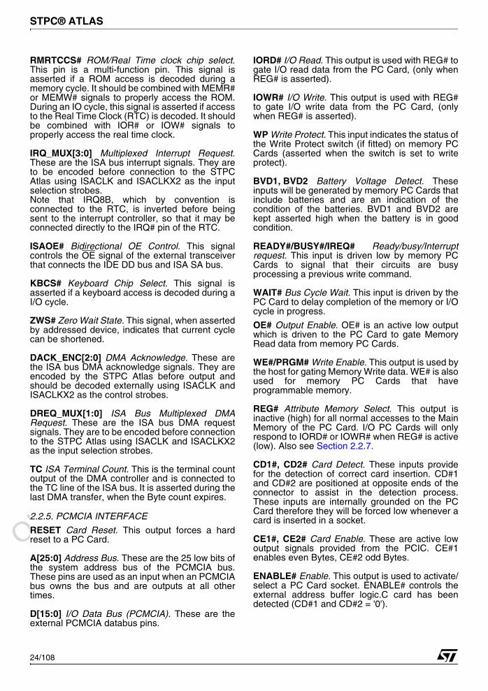
RMRTCCS# ROM/Real Time clock chip select.This pin is a multi-function pin. This signal isasserted if a ROM access is decoded during amemory cycle. It should be combined with MEMR#or MEMW# signals to properly access the ROM.During an IO cycle, this signal is asserted if accessto the Real Time Clock (RTC) is decoded. It shouldbe combined with IOR# or IOW# signals toproperly access the real time clock.
IRQ_MUX[3:0] Multiplexed Interrupt Request.These are the ISA bus interrupt signals. They areto be encoded before connection to the STPCAtlas using ISACLK and ISACLKX2 as the inputselection strobes.Note that IRQ8B, which by convention isconnected to the RTC, is inverted before beingsent to the interrupt controller, so that it may beconnected directly to the IRQ# pin of the RTC.
ISAOE# Bidirectional OE Control. This signalcontrols the OE signal of the external transceiverthat connects the IDE DD bus and ISA SA bus.
KBCS# Keyboard Chip Select. This signal isasserted if a keyboard access is decoded during aI/O cycle.
ZWS# Zero Wait State. This signal, when assertedby addressed device, indicates that current cyclecan be shortened.
DACK_ENC[2:0] DMA Acknowledge. These arethe ISA bus DMA acknowledge signals. They areencoded by the STPC Atlas before output andshould be decoded externally using ISACLK andISACLKX2 as the control strobes.
DREQ_MUX[1:0] ISA Bus Multiplexed DMARequest. These are the ISA bus DMA requestsignals. They are to be encoded before connectionto the STPC Atlas using ISACLK and ISACLKX2as the input selection strobes.
TC ISA Terminal Count. This is the terminal countoutput of the DMA controller and is connected tothe TC line of the ISA bus. It is asserted during thelast DMA transfer, when the Byte count expires.
2.2.5. PCMCIA INTERFACE
RESET Card Reset. This output forces a hardreset to a PC Card.
A[25:0] Address Bus. These are the 25 low bits ofthe system address bus of the PCMCIA bus.These pins are used as an input when an PCMCIAbus owns the bus and are outputs at all othertimes.
D[15:0] I/O Data Bus (PCMCIA). These are theexternal PCMCIA databus pins.
IORD# I/O Read. This output is used with REG# togate I/O read data from the PC Card, (only whenREG# is asserted).
IOWR# I/O Write. This output is used with REG#to gate I/O write data from the PC Card, (onlywhen REG# is asserted).
WP Write Protect. This input indicates the status ofthe Write Protect switch (if fitted) on memory PCCards (asserted when the switch is set to writeprotect).
BVD1, BVD2 Battery Voltage Detect. Theseinputs will be generated by memory PC Cards thatinclude batteries and are an indication of thecondition of the batteries. BVD1 and BVD2 arekept asserted high when the battery is in goodcondition.
READY#/BUSY#/IREQ# Ready/busy/Interruptrequest. This input is driven low by memory PCCards to signal that their circuits are busyprocessing a previous write command.
WAIT# Bus Cycle Wait. This input is driven by thePC Card to delay completion of the memory or I/Ocycle in progress.
OE# Output Enable. OE# is an active low outputwhich is driven to the PC Card to gate MemoryRead data from memory PC Cards.
WE#/PRGM# Write Enable. This output is used bythe host for gating Memory Write data. WE# is alsoused for memory PC Cards that haveprogrammable memory.
REG# Attribute Memory Select. This output isinactive (high) for all normal accesses to the MainMemory of the PC Card. I/O PC Cards will onlyrespond to IORD# or IOWR# when REG# is active(low). Also see Section 2.2.7.
CD1#, CD2# Card Detect. These inputs providefor the detection of correct card insertion. CD#1and CD#2 are positioned at opposite ends of theconnector to assist in the detection process.These inputs are internally grounded on the PCCard therefore they will be forced low whenever acard is inserted in a socket.
CE1#, CE2# Card Enable. These are active lowoutput signals provided from the PCIC. CE#1enables even Bytes, CE#2 odd Bytes.
ENABLE# Enable. This output is used to activate/select a PC Card socket. ENABLE# controls theexternal address buffer logic.C card has beendetected (CD#1 and CD#2 = '0').
1
Obsolete Product(
s) - O
bsolete Product(
s)
Obsolete Product(
s) - O
bsolete Product(
s)
STPC® ATLAS
25/108
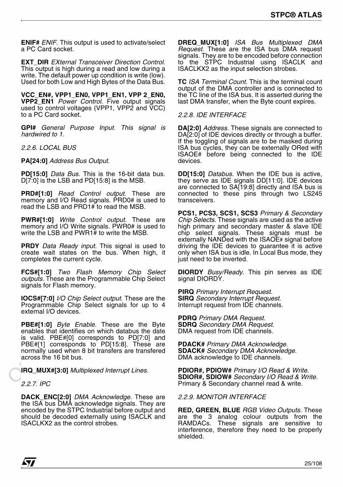
ENIF# ENIF. This output is used to activate/selecta PC Card socket.
EXT_DIR EXternal Transceiver Direction Control.This output is high during a read and low during awrite. The default power up condition is write (low).Used for both Low and High Bytes of the Data Bus.
VCC_EN#, VPP1_EN0, VPP1_EN1, VPP 2_EN0,VPP2_EN1 Power Control. Five output signalsused to control voltages (VPP1, VPP2 and VCC)to a PC Card socket.
GPI# General Purpose Input. This signal ishardwired to 1.
2.2.6. LOCAL BUS
PA[24:0] Address Bus Output.
PD[15:0] Data Bus. This is the 16-bit data bus.D[7:0] is the LSB and PD[15:8] is the MSB.
PRD#[1:0] Read Control output. These arememory and I/O Read signals. PRD0# is used toread the LSB and PRD1# to read the MSB.
PWR#[1:0] Write Control output. These arememory and I/O Write signals. PWR0# is used towrite the LSB and PWR1# to write the MSB.
PRDY Data Ready input. This signal is used tocreate wait states on the bus. When high, itcompletes the current cycle.
FCS#[1:0] Two Flash Memory Chip Selectoutputs. These are the Programmable Chip Selectsignals for Flash memory.
IOCS#[7:0] I/O Chip Select output. These are theProgrammable Chip Select signals for up to 4external I/O devices.
PBE#[1:0] Byte Enable. These are the Byteenables that identifies on which databus the dateis valid. PBE#[0] corresponds to PD[7:0] andPBE#[1] corresponds to PD[15:8]. These arenormally used when 8 bit transfers are transferedacross the 16 bit bus.
IRQ_MUX#[3:0] Multiplexed Interrupt Lines.
2.2.7. IPC
DACK_ENC[2:0] DMA Acknowledge. These arethe ISA bus DMA acknowledge signals. They areencoded by the STPC Industrial before output andshould be decoded externally using ISACLK andISACLKX2 as the control strobes.
DREQ_MUX[1:0] ISA Bus Multiplexed DMARequest. These are the ISA bus DMA requestsignals. They are to be encoded before connectionto the STPC Industrial using ISACLK andISACLKX2 as the input selection strobes.
TC ISA Terminal Count. This is the terminal countoutput of the DMA controller and is connected tothe TC line of the ISA bus. It is asserted during thelast DMA transfer, when the Byte count expires.
2.2.8. IDE INTERFACE
DA[2:0] Address. These signals are connected toDA[2:0] of IDE devices directly or through a buffer.If the toggling of signals are to be masked duringISA bus cycles, they can be externally ORed withISAOE# before being connected to the IDEdevices.
DD[15:0] Databus. When the IDE bus is active,they serve as IDE signals DD[11:0]. IDE devicesare connected to SA[19:8] directly and ISA bus isconnected to these pins through two LS245transceivers.
PCS1, PCS3, SCS1, SCS3 Primary & SecondaryChip Selects. These signals are used as the activehigh primary and secondary master & slave IDEchip select signals. These signals must beexternally NANDed with the ISAOE# signal beforedriving the IDE devices to guarantee it is activeonly when ISA bus is idle. In Local Bus mode, theyjust need to be inverted.
DIORDY Busy/Ready. This pin serves as IDEsignal DIORDY.
PIRQ Primary Interrupt Request.SIRQ Secondary Interrupt Request.Interrupt request from IDE channels.
PDRQ Primary DMA Request.SDRQ Secondary DMA Request.DMA request from IDE channels.
PDACK# Primary DMA Acknowledge.SDACK# Secondary DMA Acknowledge.DMA acknowledge to IDE channels.
PDIOR#, PDIOW# Primary I/O Read & Write.SDIOR#, SDIOW# Secondary I/O Read & Write.Primary & Secondary channel read & write.
2.2.9. MONITOR INTERFACE
RED, GREEN, BLUE RGB Video Outputs. Theseare the 3 analog colour outputs from theRAMDACs. These signals are sensitive tointerference, therefore they need to be properlyshielded.
1

Obsolete Product(
s) - O
bsolete Product(
s)
Obsolete Product(
s) - O
bsolete Product(
s)
STPC® ATLAS
26/108
VSYNC Vertical Synchronisation Pulse. This is thevertical synchronization signal from the VGAcontroller.
HSYNC Horizontal Synchronisation Pulse. This isthe horizontal synchronization signal from theVGA controller.
VREF_DAC DAC Voltage reference. This pin is aninput driving the digital to analog converters. Thisallows an external voltage reference source to beused.
RSET Resistor Current Set. This is the referencecurrent input to the RAMDAC. Used to set the full-scale output of the RAMDAC.
COMP Compensation. This is the RAMDACcompensation pin. Normally, an external capacitor(typically 10nF) is connected between this pin andVDD to damp oscillations.
DDC[1:0] Direct Data Channel Serial Link. Thesebidirectional pins are connected to CRTC register3Fh to implement DDC capabilities. They conformto I2C electrical specifications, they have open-collector output drivers which are internallyconnected to VDD through pull-up resistors.
They can instead be used for accessing I²Cdevices on board. DDC1 and DDC0 correspond toSCL and SDA respectively.
2.2.10. VIDEO INTERFACE
VCLK Pixel Clock Input.This signal is used tosynchronise data being transferred from anexternal video device to either the frame buffer, oralternatively out the TV output in bypass mode.This pin can be sourced from STPC if no externalVCLK is detected, or can be input from an externalvideo clock source.
VIN[7:0] YUV Video Data Input ITU-R 601 or 656.Time multiplexed 4:2:2 luminance andchrominance data as defined in ITU-R Rec601-2and Rec656 (except for TTL input levels). This bustypically carries a stream of Cb,Y,Cr,Y digital videoat VCLK frequency, clocked on the rising edge (bydefault) of VCLK.
VCS Line synchronisation Input. This is thehorizontal synchronisation of the incommingCCIR601 video.The signal is synchronous to rising edge of VCLK.
ODD_EVEN Frame Synchronisation Output. Thisis the vertical synchronisation of the incommingCCIR601 video.The signal is synchronous to rising edge of VCLK.The default polarity for this pin is:
- odd (not-top) field: LOW level- even (bottom) field: HIGH level
2.2.11. TFT INTERFACE SIGNALS
The TFT (Thin Film Transistor) interface convertssignals from the CRT controller into control signalsfor an external TFT Flat Panel. The signals arelisted below.
TFTFRAME, Vertical Sync. pulse Output.
TFTLINE, Horizontal Sync. Pulse Output.
TFTDE, Data Enable.
TFTR5-0, Red Output.
TFTG5-0, Green Output.
TFTB5-0, Blue Output.
TFTENVDD, Enable VDD of Flat Panel.
TFTENVCC, Enable VCC of Flat Panel.
PWM PWM Back-Light Control. This PWM isclocked by the PCI clock.
TFTDCLK, Dot clock for the Flat Panel.
2.2.12. USB INTERFACE
OC OVER CURRENT DETECT This signal isused to monitor the status of the USB powersupply lines of both devices. USB port aredisabled when OC signal is asserted.
USBDPL0, USBDMNS0 UNIVERSAL SERIALBUS DATA 0 This signal pair comprises thedifferential data signal for USB port 0.
USBDPL1, USBDMNS1 UNIVERSAL SERIALBUS PORT 1 This signal pair comprises thedifferential data signal for USB port 1.
POWERON USB power supply lines
2.2.13. SERIAL INTERFACE
RXD0, RXD1 Serial Input. Data is clocked in usingRCLK/16.
TXD0, TXD1 Serial Output. Data is clocked outusing TCLK/16 (TCLK=BAUD#).
DCD0#, DCD1# Input Data carrier detect.
RI0#, RI1# Input Ring indicator.
DSR0#, DSR1# Input Data set ready.
1
Obsolete Product(
s) - O
bsolete Product(
s)
Obsolete Product(
s) - O
bsolete Product(
s)
STPC® ATLAS
27/108
CTS0#, CTS1# Input Clear to send.
RTS0#, RTS1# Output Request to send.
DTR0#, DTR1# Output Data terminal read.
2.2.14. KEYBOARD/MOUSE INTERFACE
KBCLK, Keyboard Clock line. Keyboard data islatched by the controller on each negative clockedge produced on this pin. The keyboard can bedisabled by pulling this pin low by software control.
KBDATA, Keyboard Data Line. 11-bits of data areshifted serially through this line when data is beingtransferred. Data is synchronised to KBCLK.
MCLK, Mouse Clock line. Mouse data is latchedby the controller on each negative clock edgeproduced on this pin. The mouse can be disabledby pulling this pin low by software control.
MDATA, Mouse Data Line. 11-bits of data areshifted serially through this line when data is beingtransferred. Data is synchronised to MCLK.
2.2.15. PARALLEL PORT
PE Paper End. Input status signal from printer.
SLCT Printer Select. Printer selected input.
BUSY# Printer Busy. Input status signal from printer.
ERR# Error. Input status signal from printer.
ACK# Acknowledge. Input status signal from printer.
PDDIR# Parallel Device Direction. Bidirectional control line output.
STROBE# PCS/Strobe#. Data transfer strobe line to printer.
INIT# Initialize Printer. This output sends aninitialize command to the connected printer.
AUTOFD# Automatic Line feed. This output sendsa command to the connected printer toautomatically generate line feed on receivedcarriage returns.
SLCTIN# Select In. Printer select output.
PPD[7-0] Parallel Port Data Lines Data transferlines to printer. Bidirectional depending on modes.
2.2.16. MISCELLANEOUS
SPKRD Speaker Drive. This is the output to thespeaker and is the AND of the counter 2 outputwith bit 1 of Port 61h and drives an externalspeaker driver. This output should be connected toa 7407 type high voltage driver.
SCAN_ENABLE Reserved. This pin is reservedfor Test and Miscellaneous functions. It has to beset to ‘0’ or connected to ground in normaloperation.
2.2.17. COL_SEL Colour Select. JTAGINTERFACE
TCLK Test clock
TDI Test data input
TMS Test mode input
TDO Test data output
TRST Test reset input
2.3 SIGNAL DETAIL
The muxing between ISA, LOCAL BUS andPCMCIA is performed by external strap options.
The resulting interface is then dynamically muxedwith the IDE Interface.
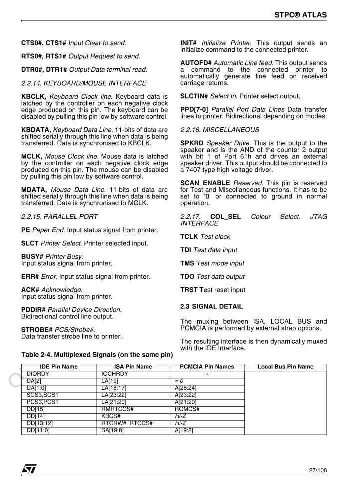
Table 2-4. Multiplexed Signals (on the same pin)
IDE Pin Name ISA Pin Name PCMCIA Pin Names Local Bus Pin NameDIORDY IOCHRDY -DA[2] LA[19] = 0DA[1:0] LA[18:17] A[25:24]SCS3,SCS1 LA[23:22] A[23:22]PCS3,PCS1 LA[21:20] A[21:20]DD[15] RMRTCCS# ROMCS#DD[14] KBCS# Hi-ZDD[13:12] RTCRW#, RTCDS# Hi-ZDD[11:0] SA[19:8] A[19:8]
1
Obsolete Product(
s) - O
bsolete Product(
s)
Obsolete Product(
s) - O
bsolete Product(
s)
STPC® ATLAS
28/108
SD[15:0] D[15:0] PD[15:0]RTCAS = 0 FCS0#DEV_CLK DEV_CLK FCS1#SA[3] A[3] PRDYSA[2:0] A[2:0] IOCS#[2:0]SMEMW# VPP_PGM PBE#[1]IOCS16# WP/IOIS16# PBE#[0]MASTER# BVD1 PRD#MCS16# = 0 PWR#DACK_ENC [2:0] = 0x04 PA[2:0]TC = 0 PA[3]SA[7:4] A[7:4] PA[7:4]ZWS# GPI# PA[8]GPIOCS# VCC5_EN PA[9]IOCHCK# BVD2 PA[10]REF# RESET PA[11]IOW# IOWR# PA[12]IOR# IORD# PA[13]MEMR# = 0 PA[14]ALE = 0 PA[15]AEN WAIT# PA[16]BHE# OE# PA[17]MEMW# = 0 PA[18]SMEMR# VCC3_EN PA[19]DREQ_MUX#[1:0] CE2#, CE1# PA[21:20]Hi-Z Hi-Z PA[22]Hi-Z VPP_VCC PA[23]Hi-Z WE# PA[24]Hi-Z REG# IOCS#[7]Hi-Z READY# IOCS#[6]Hi-Z CD1#, CD2# IOCS#[5], IOCS#[4]
ISAOE# = 1 ISAOE# = 0 ISAOE# = 0 IOCS#[3]
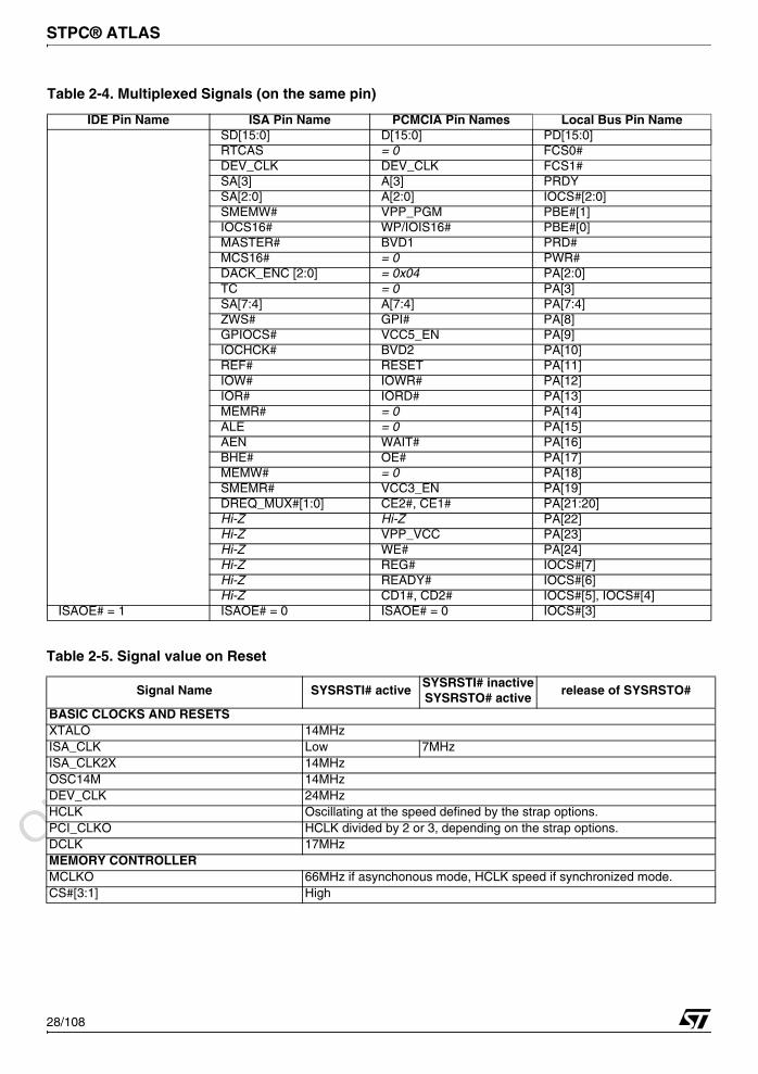
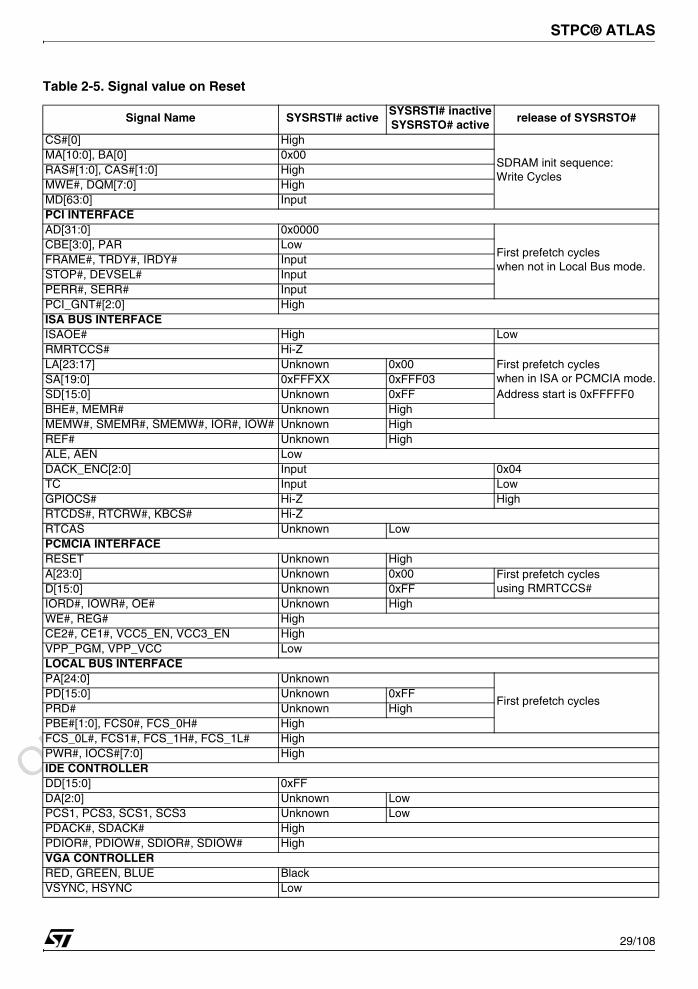
Table 2-5. Signal value on Reset
Signal Name SYSRSTI# activeSYSRSTI# inactiveSYSRSTO# active
release of SYSRSTO#
BASIC CLOCKS AND RESETSXTALO 14MHzISA_CLK Low 7MHzISA_CLK2X 14MHzOSC14M 14MHzDEV_CLK 24MHzHCLK Oscillating at the speed defined by the strap options.PCI_CLKO HCLK divided by 2 or 3, depending on the strap options.DCLK 17MHzMEMORY CONTROLLERMCLKO 66MHz if asynchonous mode, HCLK speed if synchronized mode.CS#[3:1] High
Table 2-4. Multiplexed Signals (on the same pin)
IDE Pin Name ISA Pin Name PCMCIA Pin Names Local Bus Pin Name
1
Obsolete Product(
s) - O
bsolete Product(
s)
Obsolete Product(
s) - O
bsolete Product(
s)
STPC® ATLAS
29/108
CS#[0] High
SDRAM init sequence:Write Cycles
MA[10:0], BA[0] 0x00RAS#[1:0], CAS#[1:0] HighMWE#, DQM[7:0] HighMD[63:0] InputPCI INTERFACEAD[31:0] 0x0000
First prefetch cycleswhen not in Local Bus mode.
CBE[3:0], PAR LowFRAME#, TRDY#, IRDY# InputSTOP#, DEVSEL# InputPERR#, SERR# InputPCI_GNT#[2:0] HighISA BUS INTERFACEISAOE# High LowRMRTCCS# Hi-Z
First prefetch cycleswhen in ISA or PCMCIA mode.Address start is 0xFFFFF0
LA[23:17] Unknown 0x00SA[19:0] 0xFFFXX 0xFFF03SD[15:0] Unknown 0xFFBHE#, MEMR# Unknown HighMEMW#, SMEMR#, SMEMW#, IOR#, IOW# Unknown HighREF# Unknown HighALE, AEN LowDACK_ENC[2:0] Input 0x04TC Input LowGPIOCS# Hi-Z HighRTCDS#, RTCRW#, KBCS# Hi-ZRTCAS Unknown LowPCMCIA INTERFACERESET Unknown HighA[23:0] Unknown 0x00 First prefetch cycles
using RMRTCCS#D[15:0] Unknown 0xFFIORD#, IOWR#, OE# Unknown HighWE#, REG# HighCE2#, CE1#, VCC5_EN, VCC3_EN HighVPP_PGM, VPP_VCC LowLOCAL BUS INTERFACEPA[24:0] Unknown
First prefetch cyclesPD[15:0] Unknown 0xFFPRD# Unknown HighPBE#[1:0], FCS0#, FCS_0H# HighFCS_0L#, FCS1#, FCS_1H#, FCS_1L# HighPWR#, IOCS#[7:0] HighIDE CONTROLLERDD[15:0] 0xFFDA[2:0] Unknown LowPCS1, PCS3, SCS1, SCS3 Unknown LowPDACK#, SDACK# HighPDIOR#, PDIOW#, SDIOR#, SDIOW# HighVGA CONTROLLERRED, GREEN, BLUE BlackVSYNC, HSYNC Low
Table 2-5. Signal value on Reset
Signal Name SYSRSTI# activeSYSRSTI# inactiveSYSRSTO# active
release of SYSRSTO#
1

Obsolete Product(
s) - O
bsolete Product(
s)
Obsolete Product(
s) - O
bsolete Product(
s)
STPC® ATLAS
30/108
COL_SEL UnknownI2C INTERFACESCL / DDC[1] InputSDA / DDC[0] InputTFT INTERFACE TFT[R,G,B][5:0] 0x00,0x00,0x00TFTLINE, TFTFRAME LowTFTDE, TFTENVDD, TFTENVCC, TFTPWM LowTFTDCLK Oscillating at DCLK speedUSB INTERFACEUSBDPLS[1:0]1 LowUSBDMNS[1:0]1 HighPOWERON1 Unknown LowSERIAL CONTROLLERTXD0, RTS0#, DTR0# HighTXD1, RTS1#, DTR1# HighKEYBOARD & MOUSE INTERFACEKBCLK, MCLK LowKBDATA, MDATA InputPARALLEL PORTPDIR#, INIT# LowSTROBE#, AUTOFD# HighSLCTIN# Unknown LowPPD[7:0] Unknown 0x00GPIO SIGNALSGPIO[15:0] HighJTAG TDO HighMISCELLANEOUSSPKRD Low
Table 2-5. Signal value on Reset
Signal Name SYSRSTI# activeSYSRSTI# inactiveSYSRSTO# active
release of SYSRSTO#
1

Obsolete Product(
s) - O
bsolete Product(
s)
Obsolete Product(
s) - O
bsolete Product(
s)
STPC® ATLAS
31/108
Table 2-6. Pinout
Pin# Pin NameD15 SYSRSETI#C15 SYSRSETO#AF21 XTALIAF22 XTALOAF23 PCI_CLKIAF24 PCI_CLKOE15 ISA_CLKA16 ISA_CLK2XAB18 OSC14MAB24 HCLKAB25 DEV_CLK1/FCS1#AC18 DCLK
AF20 MCLKIAF19 MCLKOU5 MA[0]V1 MA[1]V2 MA[2]V3 MA[3]V4 MA[4]V5 MA[5]W1 MA[6]W2 MA[7]W3 MA[8]W5 MA[9]Y1 MA[10]Y2 BA[0]U3 RAS#[0]U4 RAS#[1]R5 CAS#[0]T1 CAS#[1]R4 MWE#J4 MD[0]J2 MD[1]K5 MD[2]K3 MD[3]K1 MD[4]L4 MD[5]L2 MD[6]M5 MD[7]M3 MD[8]M1 MD[9]N4 MD[10]N2 MD[11]P1 MD[12]P3 MD[13]P5 MD[14]R2 MD[15]Note1; This signal is multiplexed see Table 2-4
AA4 MD[16]AB1 MD[17]AB3 MD[18]AC1 MD[19]AC3 MD[20]AD2 MD[21]AF3 MD[22]AE4 MD[23]AF4 MD[24]AD5 MD[25]AF5 MD[26]AC6 MD[27]AF6 MD[28]AC7 MD[29]AE7 MD[30]AB8 MD[31]J3 MD[32]J1 MD[33]K4 MD[34]K2 MD[35]L5 MD[36]L3 MD[37]L1 MD[38]M4 MD[39]M2 MD[40]N5 MD[41]N3 MD[42]N1 MD[43]P2 MD[44]P4 MD[45]R1 MD[46]R3 MD[47]AA5 MD[48]AB2 MD[49]AB4 MD[50]AC2 MD[51]AD1 MD[52]AE3 MD[53]AD4 MD[54]AC5 MD[55]AB6 MD[56]AE5 MD[57]AB7 MD[58]AD6 MD[59]AE6 MD[60]AD7 MD[61]AF7 MD[62]AC8 MD[63]U1 CS#[0]U2 CS#[1]
Table 2-6. Pinout
Pin# Pin Name
Note1; This signal is multiplexed see Table 2-4
1

Obsolete Product(
s) - O
bsolete Product(
s)
Obsolete Product(
s) - O
bsolete Product(
s)
STPC® ATLAS
32/108
Y3 CS#[2]/MA[11]Y4 CS#[3]/MA[12]/BA[1]T2 DQM[0]T4 DQM[1]Y5 DQM[2]AA2 DQM[3]T3 DQM[4]T5 DQM[5]AA1 DQM[6]AA3 DQM[7]
B3 AD[0]A3 AD[1]C4 AD[2]B4 AD[3]A4 AD[4]D5 AD[5]C5 AD[6]B5 AD[7]A5 AD[8]D6 AD[9]C6 AD[10]B6 AD[11]A6 AD[12]E7 AD[13]D7 AD[14]C7 AD[15]A9 AD[16]E10 AD[17]C10 AD[18]B10 AD[19]A10 AD[20]E11 AD[21]D11 AD[22]C11 AD[23]A11 AD[24]E12 AD[25]D12 AD[26]C12 AD[27]B12 AD[28]A12 AD[29]E13 AD[30]D13 AD[31]E6 CBE[0]B7 CBE[1]B9 CBE[2]B11 CBE[3]C9 FRAME#E9 TRDY#D9 IRDY#
Table 2-6. Pinout
Pin# Pin Name
Note1; This signal is multiplexed see Table 2-4
B8 STOP#A8 DEVSEL#A7 PARD8 PERR#E8 SERR#C8 LOCK#C14 PCI_REQ#[0]B14 PCI_REQ#[1]A14 PCI_REQ#[2]A13 PCI_GNT#[0]B13 PCI_GNT#[1]C13 PCI_GNT#[2]
C20 LA[17]1
B21 LA[18]1
B20 LA[19]1
E19 LA[20]1
E18 LA[21]1
C21 LA[22]1
D19 LA[23]1
P22 SA[0]1
P23 SA[1]1
P24 SA[2]1
P25 SA[3]1
P26 SA[4]1
N26 SA[5]1
N25 SA[6]1
N24 SA[7]1
N23 SA[8]1
N22 SA[9]1
M26 SA[10]1
M25 SA[11]1
M24 SA[12]1
M23 SA[13]1
M22 SA[14]1
L26 SA[15]1
L25 SA[16]1
L24 SA[17]1
L23 SA[18]1
L22 SA[19]1
K24 SD[0]1
J26 SD[1]1
J25 SD[2]1
J24 SD[3]1
K23 SD[4]1
K22 SD[5]1
H26 SD[6]1
H25 SD[7]1
H24 SD[8]1
G26 SD[9]1
Table 2-6. Pinout
Pin# Pin Name
Note1; This signal is multiplexed see Table 2-4
1
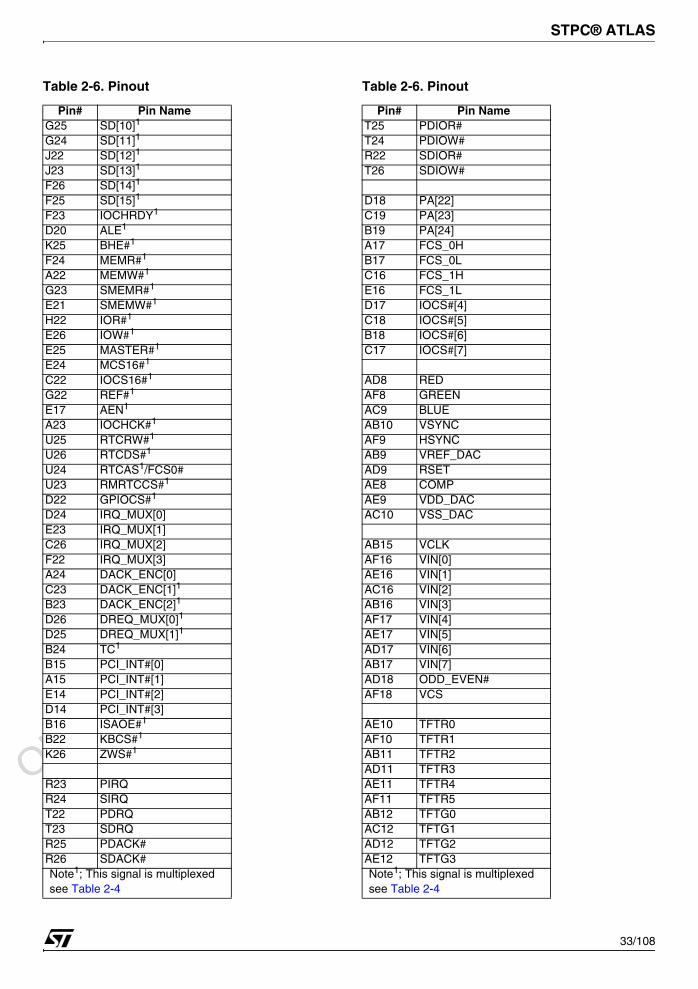
Obsolete Product(
s) - O
bsolete Product(
s)
Obsolete Product(
s) - O
bsolete Product(
s)
STPC® ATLAS
33/108
G25 SD[10]1
G24 SD[11]1
J22 SD[12]1
J23 SD[13]1
F26 SD[14]1
F25 SD[15]1
F23 IOCHRDY1
D20 ALE1
K25 BHE#1
F24 MEMR#1
A22 MEMW#1
G23 SMEMR#1
E21 SMEMW#1
H22 IOR#1
E26 IOW#1
E25 MASTER#1
E24 MCS16#1
C22 IOCS16#1
G22 REF#1
E17 AEN1
A23 IOCHCK#1
U25 RTCRW#1
U26 RTCDS#1
U24 RTCAS1/FCS0#U23 RMRTCCS#1
D22 GPIOCS#1
D24 IRQ_MUX[0]E23 IRQ_MUX[1]C26 IRQ_MUX[2]F22 IRQ_MUX[3]A24 DACK_ENC[0]C23 DACK_ENC[1]1
B23 DACK_ENC[2]1
D26 DREQ_MUX[0]1
D25 DREQ_MUX[1]1
B24 TC1
B15 PCI_INT#[0]A15 PCI_INT#[1]E14 PCI_INT#[2]D14 PCI_INT#[3]B16 ISAOE#1
B22 KBCS#1
K26 ZWS#1
R23 PIRQR24 SIRQT22 PDRQT23 SDRQR25 PDACK#R26 SDACK#
Table 2-6. Pinout
Pin# Pin Name
Note1; This signal is multiplexed see Table 2-4
T25 PDIOR#T24 PDIOW#R22 SDIOR#T26 SDIOW#
D18 PA[22]C19 PA[23]B19 PA[24]A17 FCS_0HB17 FCS_0LC16 FCS_1HE16 FCS_1LD17 IOCS#[4]C18 IOCS#[5]B18 IOCS#[6]C17 IOCS#[7]
AD8 REDAF8 GREENAC9 BLUEAB10 VSYNCAF9 HSYNCAB9 VREF_DACAD9 RSETAE8 COMPAE9 VDD_DACAC10 VSS_DAC
AB15 VCLKAF16 VIN[0]AE16 VIN[1]AC16 VIN[2]AB16 VIN[3]AF17 VIN[4]AE17 VIN[5]AD17 VIN[6]AB17 VIN[7]AD18 ODD_EVEN#AF18 VCS
AE10 TFTR0AF10 TFTR1AB11 TFTR2AD11 TFTR3AE11 TFTR4AF11 TFTR5AB12 TFTG0AC12 TFTG1AD12 TFTG2AE12 TFTG3
Table 2-6. Pinout
Pin# Pin Name
Note1; This signal is multiplexed see Table 2-4
1
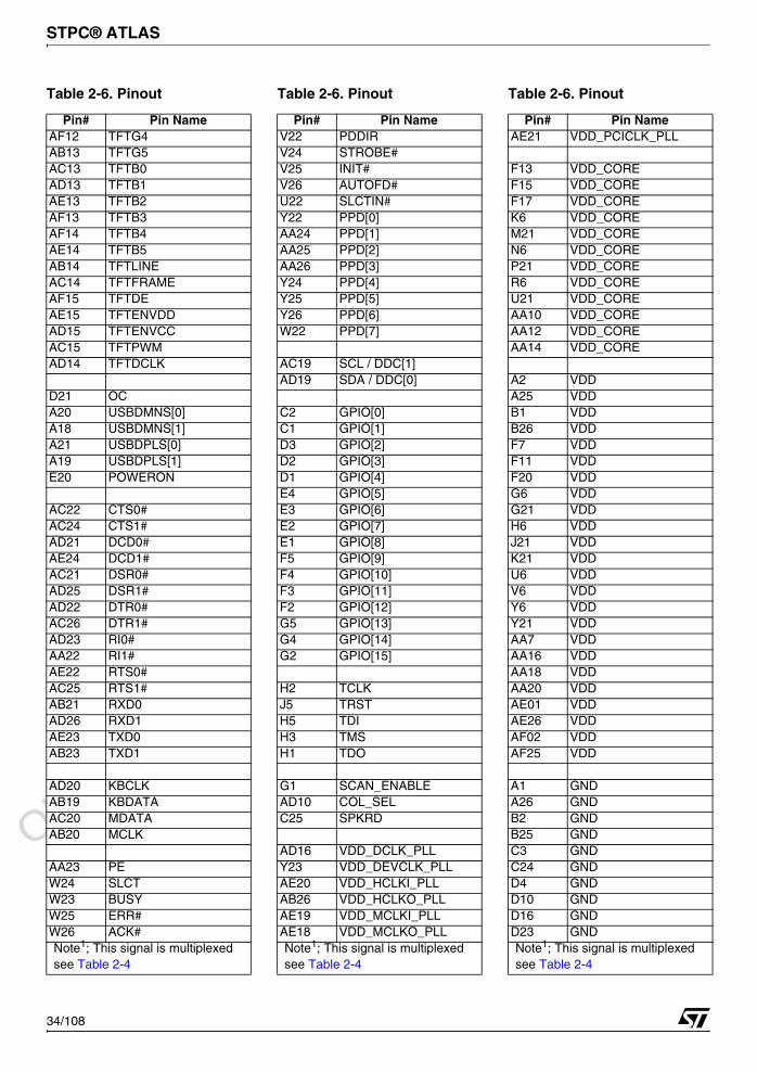
Obsolete Product(
s) - O
bsolete Product(
s)
Obsolete Product(
s) - O
bsolete Product(
s)
STPC® ATLAS
34/108
AF12 TFTG4AB13 TFTG5AC13 TFTB0AD13 TFTB1AE13 TFTB2AF13 TFTB3AF14 TFTB4AE14 TFTB5AB14 TFTLINEAC14 TFTFRAMEAF15 TFTDEAE15 TFTENVDDAD15 TFTENVCCAC15 TFTPWMAD14 TFTDCLK
D21 OCA20 USBDMNS[0]A18 USBDMNS[1]A21 USBDPLS[0]A19 USBDPLS[1]E20 POWERON
AC22 CTS0#AC24 CTS1#AD21 DCD0#AE24 DCD1#AC21 DSR0#AD25 DSR1#AD22 DTR0#AC26 DTR1#AD23 RI0#AA22 RI1#AE22 RTS0#AC25 RTS1#AB21 RXD0AD26 RXD1AE23 TXD0AB23 TXD1
AD20 KBCLKAB19 KBDATAAC20 MDATAAB20 MCLK
AA23 PEW24 SLCTW23 BUSYW25 ERR#W26 ACK#
Table 2-6. Pinout
Pin# Pin Name
Note1; This signal is multiplexed see Table 2-4
V22 PDDIRV24 STROBE#V25 INIT#V26 AUTOFD#U22 SLCTIN#Y22 PPD[0]AA24 PPD[1]AA25 PPD[2]AA26 PPD[3]Y24 PPD[4]Y25 PPD[5]Y26 PPD[6]W22 PPD[7]
AC19 SCL / DDC[1]AD19 SDA / DDC[0]
C2 GPIO[0]C1 GPIO[1]D3 GPIO[2]D2 GPIO[3]D1 GPIO[4]E4 GPIO[5]E3 GPIO[6]E2 GPIO[7]E1 GPIO[8]F5 GPIO[9]F4 GPIO[10]F3 GPIO[11]F2 GPIO[12]G5 GPIO[13]G4 GPIO[14]G2 GPIO[15]
H2 TCLKJ5 TRSTH5 TDIH3 TMSH1 TDO
G1 SCAN_ENABLEAD10 COL_SELC25 SPKRD
AD16 VDD_DCLK_PLLY23 VDD_DEVCLK_PLLAE20 VDD_HCLKI_PLLAB26 VDD_HCLKO_PLLAE19 VDD_MCLKI_PLLAE18 VDD_MCLKO_PLL
Table 2-6. Pinout
Pin# Pin Name
Note1; This signal is multiplexed see Table 2-4
AE21 VDD_PCICLK_PLL
F13 VDD_COREF15 VDD_COREF17 VDD_COREK6 VDD_COREM21 VDD_COREN6 VDD_COREP21 VDD_CORER6 VDD_COREU21 VDD_COREAA10 VDD_COREAA12 VDD_COREAA14 VDD_CORE
A2 VDDA25 VDDB1 VDDB26 VDDF7 VDDF11 VDDF20 VDDG6 VDDG21 VDDH6 VDDJ21 VDDK21 VDDU6 VDDV6 VDDY6 VDDY21 VDDAA7 VDDAA16 VDDAA18 VDDAA20 VDDAE01 VDDAE26 VDDAF02 VDDAF25 VDD
A1 GNDA26 GNDB2 GNDB25 GNDC3 GNDC24 GNDD4 GNDD10 GNDD16 GNDD23 GND
Table 2-6. Pinout
Pin# Pin Name
Note1; This signal is multiplexed see Table 2-4
1

Obsolete Product(
s) - O
bsolete Product(
s)
Obsolete Product(
s) - O
bsolete Product(
s)
STPC® ATLAS
35/108
E5 GNDE22 GNDF6 GNDF8 GNDF9 GNDF10 GNDF12 GNDF14 GNDF16 GNDF18 GNDF19 GNDF21 GNDH4 GNDH21 GNDH23 GNDJ6 GNDL6 GNDL11:16 GNDL21 GNDM6 GNDM11:16 GNDN11:16 GND
Table 2-6. Pinout
Pin# Pin Name
Note1; This signal is multiplexed see Table 2-4
N21 GNDP6 GNDP11:16 GNDR11:16 GNDR21 GNDT6 GNDT11:16 GNDT21 GNDV21 GNDV23 GNDW4 GNDW6 GNDW21 GNDAA6 GNDAA8 GNDAA9 GNDAA11 GNDAA13 GNDAA15 GNDAA17 GNDAA19 GNDAA21 GND
Table 2-6. Pinout
Pin# Pin Name
Note1; This signal is multiplexed see Table 2-4
AB5 GNDAB22 GNDAC4 GNDAC11 GNDAC17 GNDAC23 GNDAD3 GNDAD24 GNDAE2 GNDAE25 GNDAF1 GNDAF26 GND
G3 ReservedF1 Reserved
Table 2-6. Pinout
Pin# Pin Name
Note1; This signal is multiplexed see Table 2-4
1
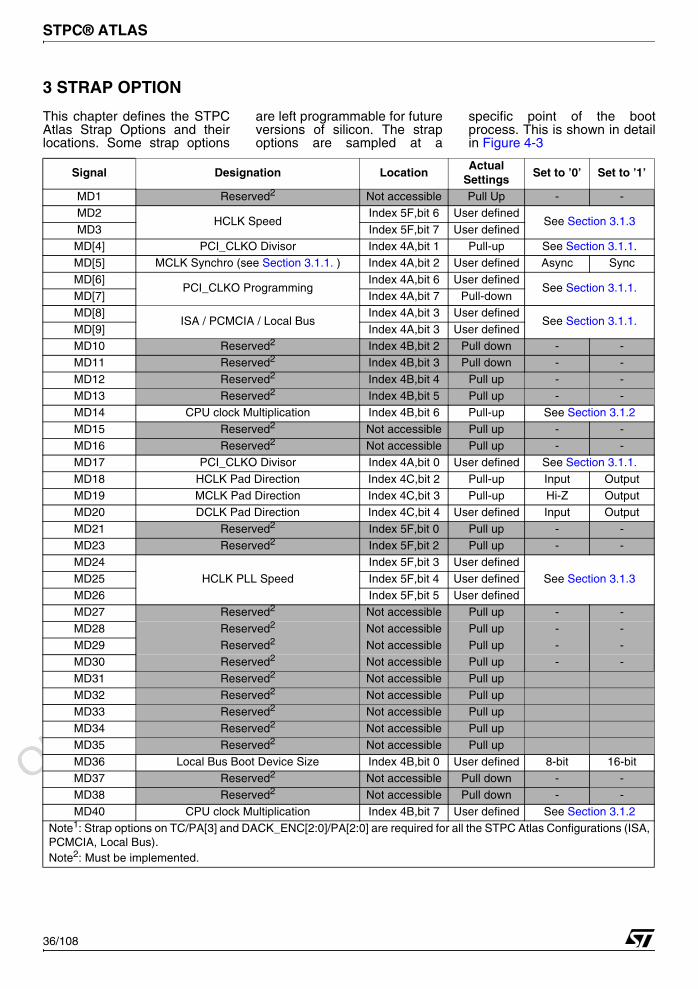
Obsolete Product(
s) - O
bsolete Product(
s)
Obsolete Product(
s) - O
bsolete Product(
s)
STPC® ATLAS
36/108
3 STRAP OPTION
This chapter defines the STPCAtlas Strap Options and theirlocations. Some strap options
are left programmable for futureversions of silicon. The strapoptions are sampled at a
specific point of the bootprocess. This is shown in detailin Figure 4-3
Signal Designation LocationActual
SettingsSet to ’0’ Set to ’1’
MD1 Reserved2 Not accessible Pull Up - -MD2
HCLK SpeedIndex 5F,bit 6 User defined
See Section 3.1.3 MD3 Index 5F,bit 7 User definedMD[4] PCI_CLKO Divisor Index 4A,bit 1 Pull-up See Section 3.1.1. MD[5] MCLK Synchro (see Section 3.1.1. ) Index 4A,bit 2 User defined Async SyncMD[6]
PCI_CLKO ProgrammingIndex 4A,bit 6 User defined
See Section 3.1.1. MD[7] Index 4A,bit 7 Pull-downMD[8]
ISA / PCMCIA / Local BusIndex 4A,bit 3 User defined
See Section 3.1.1. MD[9] Index 4A,bit 3 User definedMD10 Reserved2 Index 4B,bit 2 Pull down - -MD11 Reserved2 Index 4B,bit 3 Pull down - -MD12 Reserved2 Index 4B,bit 4 Pull up - -MD13 Reserved2 Index 4B,bit 5 Pull up - -MD14 CPU clock Multiplication Index 4B,bit 6 Pull-up See Section 3.1.2 MD15 Reserved2 Not accessible Pull up - -MD16 Reserved2 Not accessible Pull up - -MD17 PCI_CLKO Divisor Index 4A,bit 0 User defined See Section 3.1.1. MD18 HCLK Pad Direction Index 4C,bit 2 Pull-up Input OutputMD19 MCLK Pad Direction Index 4C,bit 3 Pull-up Hi-Z OutputMD20 DCLK Pad Direction Index 4C,bit 4 User defined Input OutputMD21 Reserved2 Index 5F,bit 0 Pull up - -MD23 Reserved2 Index 5F,bit 2 Pull up - -MD24
HCLK PLL SpeedIndex 5F,bit 3 User defined
See Section 3.1.3 MD25 Index 5F,bit 4 User definedMD26 Index 5F,bit 5 User definedMD27 Reserved2 Not accessible Pull up - -MD28 Reserved2 Not accessible Pull up - -MD29 Reserved2 Not accessible Pull up - -MD30 Reserved2 Not accessible Pull up - -MD31 Reserved2 Not accessible Pull upMD32 Reserved2 Not accessible Pull upMD33 Reserved2 Not accessible Pull upMD34 Reserved2 Not accessible Pull upMD35 Reserved2 Not accessible Pull upMD36 Local Bus Boot Device Size Index 4B,bit 0 User defined 8-bit 16-bitMD37 Reserved2 Not accessible Pull down - -MD38 Reserved2 Not accessible Pull down - -MD40 CPU clock Multiplication Index 4B,bit 7 User defined See Section 3.1.2
Note1: Strap options on TC/PA[3] and DACK_ENC[2:0]/PA[2:0] are required for all the STPC Atlas Configurations (ISA, PCMCIA, Local Bus).Note2: Must be implemented.
1

Obsolete Product(
s) - O
bsolete Product(
s)
Obsolete Product(
s) - O
bsolete Product(
s)
STPC® ATLAS
37/108
MD41 Reserved2 Not accessible Pull down - -MD42 Reserved2 Not accessible Pull up - -MD 43 Reserved2 Not accessible Pull down - -MD 45
CPUCLK/HCKL Deskew ProgrammingNot accessible User defined
See Section 3.1.5 MD 46 Not accessible User definedMD 47 Reserved2 Not accessible Pull down - -MD 48 Reserved2 Not accessible Pull up - -MD 50 Internal UART2 (see Section 3.1.4. ) Index 4C,bit 0 User defined Disable EnableMD 51 Internal UART1 (see Section 3.1.4. ) Index 4C,bit 1 User defined Disable EnableMD 52 Internal Kbd / Mouse (see Section 3.1.4. ) Index 4C,bit 6 User defined Disable EnableMD 53 Internal Parallel Port (see Section 3.1.4. ) Index 4C,bit 7 User defined Disable Enable
TC1 Reserved2 Hardware Pull up - -DACK_ENC[2]1 Reserved2 Hardware Pull up - -DACK_ENC[1]1 Reserved2 Hardware Pull up - -DACK_ENC[0]1 Reserved2 Hardware Pull up - -
Signal Designation LocationActual
SettingsSet to ’0’ Set to ’1’
Note1: Strap options on TC/PA[3] and DACK_ENC[2:0]/PA[2:0] are required for all the STPC Atlas Configurations (ISA, PCMCIA, Local Bus).Note2: Must be implemented.
1

Obsolete Product(
s) - O
bsolete Product(
s)
Obsolete Product(
s) - O
bsolete Product(
s)
STPC® ATLAS
38/108
3.1 STRAP OPTION REGISTER DESCRIPTION
3.1.1. STRAP REGISTER 0
This register is read only.
STRAP0 Access = 0022h/0023h Regoffset =04Ah
7 6 5 4 3 2 1 0
MD[7] MD[6] MD[9] MD[8] RSV MD[5] MD[4] MD[17]
This register defaults to the values sampled on the MD pins after reset
Bit Number Sampled Mnemonic Description
Bits 7-6 MD[7:6]
PCICLK PLL set-up: The value sampled on MD[7:6] controls the PCICLK PLL programming according to the PCICLK frequency.MD7 MD6
0 0 PCICLK frequency between 16 & 32 MHz0 1 PCICLK frequency between 32 & 64 MHz1 X Reserved
Bits 5-4 MD[9:8]
Mode selection:MD9 MD8
0 0 ISA mode: ISA enabled, PCMCIA & Local Bus disabled0 1 PCMCIA mode: PCMCIA enabled, ISA & Local Bus disabled1 0 Local Bus mode: Local Bus enabled, ISA & PCMCIA disabled1 1 Reserved
Bit 3 Rsv Reserved
Bit 2 MD[5]
Host Memory synchronization. This bit reflects the value sampled on [MD5] and controls the MCLK/HCLK synchronization.
0: MCLK and HCLK not synchronized1: MCLK and HCLK synchronized.
Bits 1-0 MD[4], MD[17]
PCICLK division: These bits reflect the values sampled on [MD4] and MD[17] to select the PCICLK frequency. MD4 MD17
0 X PCI Clock output = HCLK / 41 0 PCI Clock output = HCLK / 31 1 PCI Clock output = HCLK / 2
1
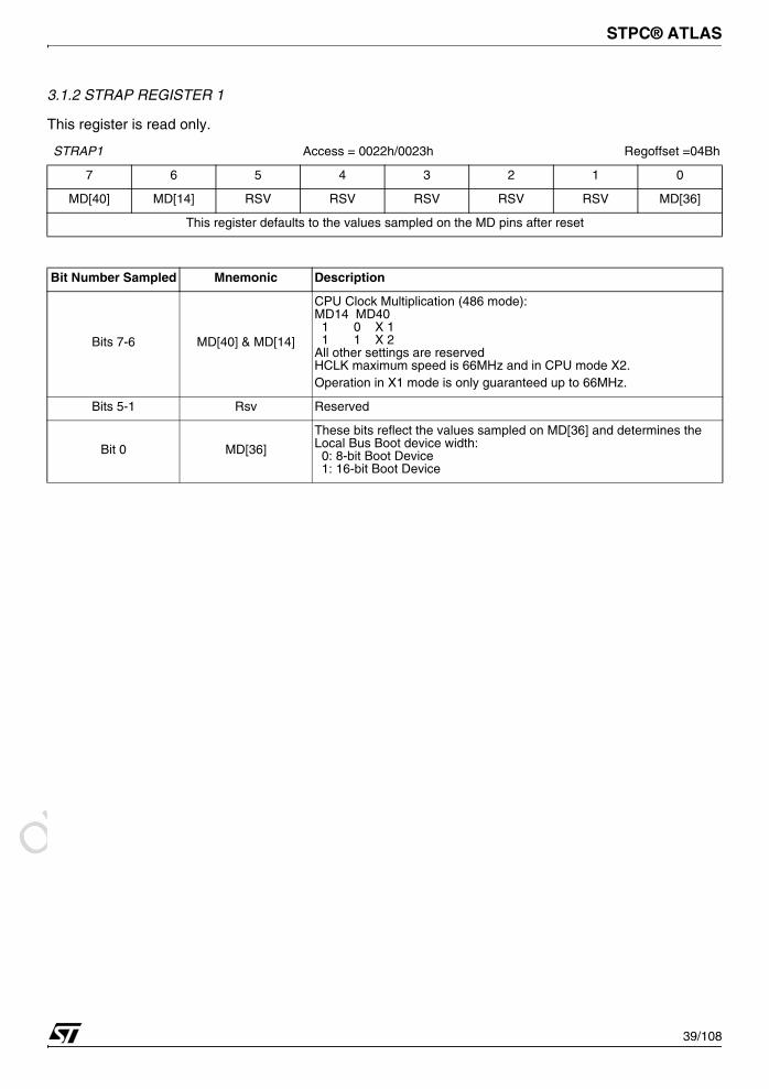
Obsolete Product(
s) - O
bsolete Product(
s)
Obsolete Product(
s) - O
bsolete Product(
s)
STPC® ATLAS
39/108
3.1.2 STRAP REGISTER 1
This register is read only.
STRAP1 Access = 0022h/0023h Regoffset =04Bh
7 6 5 4 3 2 1 0
MD[40] MD[14] RSV RSV RSV RSV RSV MD[36]
This register defaults to the values sampled on the MD pins after reset
Bit Number Sampled Mnemonic Description
Bits 7-6 MD[40] & MD[14]
CPU Clock Multiplication (486 mode):MD14 MD40
1 0 X 11 1 X 2
All other settings are reservedHCLK maximum speed is 66MHz and in CPU mode X2. Operation in X1 mode is only guaranteed up to 66MHz.
Bits 5-1 Rsv Reserved
Bit 0 MD[36]
These bits reflect the values sampled on MD[36] and determines the Local Bus Boot device width:
0: 8-bit Boot Device1: 16-bit Boot Device
1
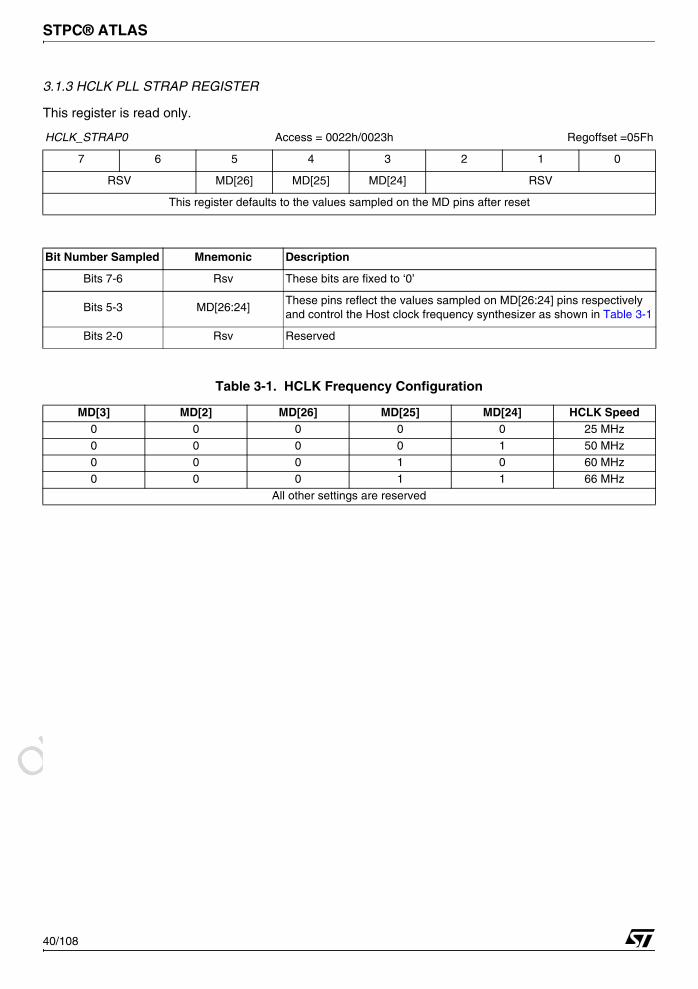
Obsolete Product(
s) - O
bsolete Product(
s)
Obsolete Product(
s) - O
bsolete Product(
s)
STPC® ATLAS
40/108
3.1.3 HCLK PLL STRAP REGISTER
This register is read only.
HCLK_STRAP0 Access = 0022h/0023h Regoffset =05Fh
7 6 5 4 3 2 1 0
RSV MD[26] MD[25] MD[24] RSV
This register defaults to the values sampled on the MD pins after reset
Bit Number Sampled Mnemonic Description
Bits 7-6 Rsv These bits are fixed to ‘0’
Bits 5-3 MD[26:24]These pins reflect the values sampled on MD[26:24] pins respectively and control the Host clock frequency synthesizer as shown in Table 3-1
Bits 2-0 Rsv Reserved
Table 3-1. HCLK Frequency Configuration
MD[3] MD[2] MD[26] MD[25] MD[24] HCLK Speed0 0 0 0 0 25 MHz0 0 0 0 1 50 MHz0 0 0 1 0 60 MHz0 0 0 1 1 66 MHz
All other settings are reserved
1

Obsolete Product(
s) - O
bsolete Product(
s)
Obsolete Product(
s) - O
bsolete Product(
s)
STPC® ATLAS
41/108
3.1.4. STRAP REGISTER 2
This register is read only with the exception of bit 4
STRAP2 Access = 0022h/0023h Regoffset =04Ch
7 6 5 4 3 2 1 0
MD[53] MD[52] RSV MD[20] MD[19] MD[18] MD[51] MD[50]
This register defaults to the values sampled on the MD pins after reset
Bit Number Sampled Mnemonic Description
Bit 7 MD[53]
This bit reflects the value sampled on MD[53] pin and determines whether the internal Parallel Port Controller is used0: Internal Parallel Port Controller is disabled1: Internal Parallel Port Controller is enabled
Bit 6 MD[52]
This bit reflects the value sampled on MD[52] pin and determines whether the internal Keyboard controller is used0: Internal Keyboard Controller is disabled1: Internal Keyboard Controller is enabled
Bit 5 Rsv Reserved
Bit 4 MD[20]
This bit reflects the value sampled on MD[20] pin and controls the Dot clock pin (DCLK) direction as follows:0: Input.1: Output of the internal frequency synthesizer DCLK PLL.
Bit 3 MD[19]
This bit reflects the value sampled on MD[19] pin and controls the Memory clock output pin (MCLKO) as follows:0: Tristated.1: Output of the internal frequency synthesizer MCLKO PLL.
Bit 2 MD[18]
This bit reflects the value sampled on MD[18] pin and controls the Host clock pin (HCLK) direction as follows:0: Input.1: Output of the internal frequency synthesizer HCLK PLL.
Bit 1 MD[51]
This bit reflects the value sampled on MD[51] pin and determines whether the internal UART1 is enabled:0: Internal UART1 is disabled1: Internal UART1 is enabled
Bit 0 MD[50]
This bit reflects the value sampled on MD[50] pin and determines whether the internal UART2 is enabled:0: Internal UART2 is disabled1: Internal UART2 is enabled
1

Obsolete Product(
s) - O
bsolete Product(
s)
Obsolete Product(
s) - O
bsolete Product(
s)
STPC® ATLAS
42/108
3.1.5 CPUCLK/HCKL DESKEW PROGRAMMING
Note that these straps are not accessible bysoftware.
3.2 TYPICAL STRAP OPTION IMPLEMENTATION
Table 3-1.shows the detailed Strap optionsrequired to boot the STPC in ISA mode with a HostClock Frequency of 66MHz in X2 mode withinternal keyboard/mouse, UARTS and parallel portenabled.
MD[45] MD[46] Description
1 0HCLK between 33MHz and
64MHz
0 1HCLK between 64MHz and
133MHz
All other settings are reserved
Table 3-1. Typical Strap Option Implementation
Signal DesignationActual
SettingsDescription
MD1 Reserved2 Pull Up -MD2
HCLK SpeedPull down
HCLK = 66MHzMD3 Pull downMD[4] PCI_CLKO Divisor Pull up PCICLK = HCLK/2MD[5] MCLK Synchro (see Section 3.1.1. ) Pull down AsynchronousMD[6]
PCI_CLKO ProgrammingPull up PCICLK PLL Window =
32MHz - 64MHzMD[7] Pull downMD[8]
ISA / PCMCIA / Local BusPull down
ISA ModeMD[9] Pull downMD10 Reserved2 Pull down -MD11 Reserved2 Pull down -MD14 CPU clock Multiplication Pull up X2 Mode MD15 Reserved2 Pull up -MD16 Reserved2 Pull up -MD17 PCI_CLKO Divisor Pull up PCICLK = HCLK/2MD18 HCLK Pad Direction Pull up OutputMD19 MCLK Pad Direction Pull up OutputMD20 DCLK Pad Direction Pull up OutputMD21 Reserved2 Pull up -MD23 Reserved2 Pull up -MD24
HCLK PLL SpeedPull up
HCLK = 66MHzMD25 Pull upMD26 Pull downMD27 Reserved2 Pull up -MD28 Reserved2 Pull up -MD29 Reserved2 Pull up -MD30 Reserved2 Pull up -MD31 Reserved2 Pull upMD32 Reserved2 Pull upMD33 Reserved2 Pull upMD34 Reserved2 Pull up
Note1: Strap options on TC/PA[3] and DACK_ENC[2:0]/PA[2:0] are required for all the STPC Atlas Configurations (ISA, PCMCIA, Local Bus).Note2: Must be implemented.
1

Obsolete Product(
s) - O
bsolete Product(
s)
Obsolete Product(
s) - O
bsolete Product(
s)
STPC® ATLAS
43/108
MD35 Reserved2 Pull upMD36 Local Bus Boot Device Size User defined Not ApplicableMD37 Reserved2 Pull down -MD38 Reserved2 Pull down -MD40 CPU clock Multiplication Pull up X2 modeMD41 Reserved2 Pull down -MD42 Reserved2 Pull up -MD 43 Reserved2 Pull down -MD 45
CPUCLK/HCKL Deskew ProgrammingPull down HCLK between 64MHz and
133MHzMD 46 Pull upMD 47 Reserved2 Pull down -MD 48 Reserved2 Pull up -MD 50 Internal UART2 (see Section 3.1.4. ) Pull up EnableMD 51 Internal UART1 (see Section 3.1.4. ) Pull up EnableMD 52 Internal Kbd / Mouse (see Section 3.1.4. ) Pull up EnableMD 53 Internal Parallel Port (see Section 3.1.4. ) Pull up Enable
TC1 Reserved2 Pull up -DACK_ENC[2]1 Reserved2 Pull up -DACK_ENC[1]1 Reserved2 Pull up -DACK_ENC[0]1 Reserved2 Pull up -
Table 3-1. Typical Strap Option Implementation
Signal DesignationActual
SettingsDescription
Note1: Strap options on TC/PA[3] and DACK_ENC[2:0]/PA[2:0] are required for all the STPC Atlas Configurations (ISA, PCMCIA, Local Bus).Note2: Must be implemented.
1

Obsolete Product(
s) - O
bsolete Product(
s)
Obsolete Product(
s) - O
bsolete Product(
s)
STPC® ATLAS
44/108
4 ELECTRICAL SPECIFICATIONS
4.1. INTRODUCTION
The electrical specifications in this chapter arevalid for the STPC Atlas.
4.2. ELECTRICAL CONNECTIONS
4.2.1. POWER/GROUND CONNECTIONS/DECOUPLING
Due to the high frequency of operation of theSTPC Atlas, it is necessary to install and test thisdevice using standard high frequency techniques.The high clock frequencies used in the STPC Atlasand its output buffer circuits can cause transientpower surges when several output buffers switchoutput levels simultaneously. These effects can beminimized by filtering the DC power leads withlow-inductance decoupling capacitors, using lowimpedance wiring, and by utilizing all of the VSSand VDD pins.
4.2.2. UNUSED INPUT PINS
No unused input pin should be left unconnectedunless they have an integrated pull-up or pull-down. Connect active-low inputs to VDD through a20 kΩ (±10%) pull-up resistor and active-highinputs to VSS. For bi-directionnal active-highinputs, connect to VSS through a 20 kΩ (±10%)pull-up resistor to prevent spurious operation.
4.2.3. RESERVED DESIGNATED PINS
Pins designated as reserved should be left dis-connected. Connecting a reserved pin to a pull-upresistor, pull-down resistor, or an active signalcould cause unexpected results and possiblecircuit malfunctions.
4.3. ABSOLUTE MAXIMUM RATINGS
The following table lists the absolute maximumratings for the STPC Atlas device. Stressesbeyond those listed under Table 4-1 limits maycause permanent damage to the device. Theseare stress ratings only and do not imply thatoperation under any conditions other than thosespecified in section "Operating Conditions".
Exposure to conditions beyond those outlined inTable 4-1 may (1) reduce device reliability and (2)result in premature failure even when there is noimmediately apparent sign of failure. Prolongedexposure to conditions at or near the absolutemaximum ratings (Table 4-1) may also result inreduced useful life and reliability.
4.3.1. 5V TOLERANCE
The STPC is capable of running with I/O systemsthat operate at 5 V such as PCI and ISA devices.Certain pins of the STPC tolerate inputs up to5.5 V. Above this limit the component is likely tosustain permanent damage.
All 5 volt tolerant pins are outlined in Table 2-3Buffer Type Descriptions.
Note 1: The figures specified apply to the Tcase of aSTPC device that is soldered to a board, as detailed in the
Design Guidelines Section, for Commercial and Industrialtemperature ranges.
Table 4-1. Absolute Maximum Ratings
Symbol Parameter Minimum Maximum UnitsVDDx DC Supply Voltage -0.3 4.0 V
VCORE DC Supply Voltage for Core -0.3 2.7 VVI, VO Digital Input and Output Voltage -0.3 VDD + 0.3 V
V5T 5Volt Tolerance -0.3 5.5 VVESD ESD Capacity (Human body mode) - 2000 VTSTG Storage Temperature -40 +150 °C
TOPER Operating Temperature (Note 1)0 +85 °C
-40 +115 °CPTOT Maximum Power Dissipation (package) - 4.8 W
1
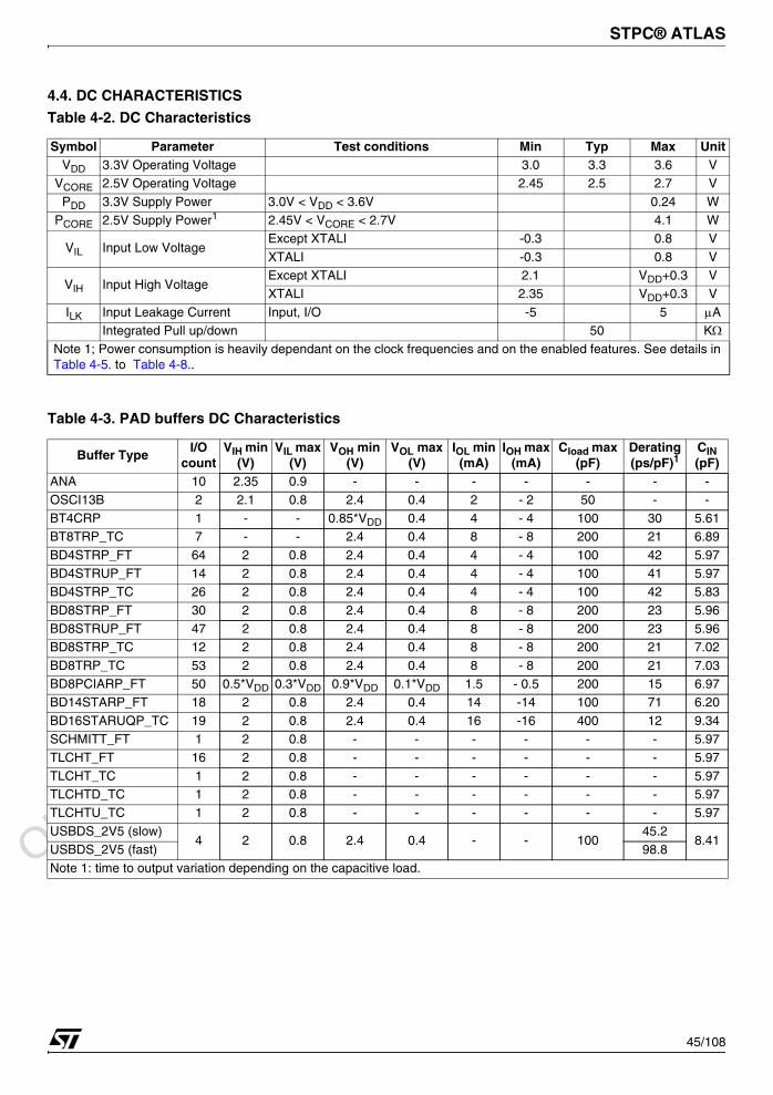
Obsolete Product(
s) - O
bsolete Product(
s)
Obsolete Product(
s) - O
bsolete Product(
s)
STPC® ATLAS
45/108
4.4. DC CHARACTERISTICS
Table 4-2. DC Characteristics
Symbol Parameter Test conditions Min Typ Max UnitVDD 3.3V Operating Voltage 3.0 3.3 3.6 V
VCORE 2.5V Operating Voltage 2.45 2.5 2.7 VPDD 3.3V Supply Power 3.0V < VDD < 3.6V 0.24 W
PCORE 2.5V Supply Power1 2.45V < VCORE < 2.7V 4.1 W
VIL Input Low VoltageExcept XTALI -0.3 0.8 VXTALI -0.3 0.8 V
VIH Input High VoltageExcept XTALI 2.1 VDD+0.3 VXTALI 2.35 VDD+0.3 V
ILK Input Leakage Current Input, I/O -5 5 µAIntegrated Pull up/down 50 KΩ
Note 1; Power consumption is heavily dependant on the clock frequencies and on the enabled features. See details in Table 4-5. to Table 4-8..
Table 4-3. PAD buffers DC Characteristics
Buffer TypeI/O
countVIH min
(V)VIL max
(V)VOH min
(V)VOL max
(V)IOL min(mA)
IOH max(mA)
Cload max(pF)
Derating(ps/pF)1
CIN(pF)
ANA 10 2.35 0.9 - - - - - - -OSCI13B 2 2.1 0.8 2.4 0.4 2 - 2 50 - -BT4CRP 1 - - 0.85*VDD 0.4 4 - 4 100 30 5.61BT8TRP_TC 7 - - 2.4 0.4 8 - 8 200 21 6.89BD4STRP_FT 64 2 0.8 2.4 0.4 4 - 4 100 42 5.97BD4STRUP_FT 14 2 0.8 2.4 0.4 4 - 4 100 41 5.97BD4STRP_TC 26 2 0.8 2.4 0.4 4 - 4 100 42 5.83BD8STRP_FT 30 2 0.8 2.4 0.4 8 - 8 200 23 5.96BD8STRUP_FT 47 2 0.8 2.4 0.4 8 - 8 200 23 5.96BD8STRP_TC 12 2 0.8 2.4 0.4 8 - 8 200 21 7.02BD8TRP_TC 53 2 0.8 2.4 0.4 8 - 8 200 21 7.03BD8PCIARP_FT 50 0.5*VDD 0.3*VDD 0.9*VDD 0.1*VDD 1.5 - 0.5 200 15 6.97BD14STARP_FT 18 2 0.8 2.4 0.4 14 -14 100 71 6.20BD16STARUQP_TC 19 2 0.8 2.4 0.4 16 -16 400 12 9.34SCHMITT_FT 1 2 0.8 - - - - - - 5.97TLCHT_FT 16 2 0.8 - - - - - - 5.97TLCHT_TC 1 2 0.8 - - - - - - 5.97TLCHTD_TC 1 2 0.8 - - - - - - 5.97TLCHTU_TC 1 2 0.8 - - - - - - 5.97USBDS_2V5 (slow)
4 2 0.8 2.4 0.4 - - 10045.2
8.41USBDS_2V5 (fast) 98.8Note 1: time to output variation depending on the capacitive load.
1

Obsolete Product(
s) - O
bsolete Product(
s)
Obsolete Product(
s) - O
bsolete Product(
s)
STPC® ATLAS
46/108
Note 1: PCI clock at 33MHz
Table 4-4. RAMDAC DC Specification
Symbol Parameter Min MaxVref_dac Voltage Reference 1.00 V 1.24 V
INL Integrated Non Linear Error - 3 LSBDNL Differentiated Non Linear Error - 1 LSBBLC Black Level Current 1.0 mA 2.0 mAWLC White Level Current 15.00 mA 18.50 mA
Table 4-5. VGA RAMDAC Power Consumption
DCLK
(MHz)
DAC mode
(State)
PMax (mW)VDD_DAC = 2.45V VDD_DAC = 2.7V
- Shutdown 0 06.25 - 135 Active 150 180
Table 4-6. 2.5V Power Consumptions (VCORE + VDD_x_PLL + VDD_DAC)
HCLK
(MHz)
CPUCLK
(MHz)
MCLK
(MHz)Mode
DCLK
(MHz)
PMU
(State)
PMax (W)V2.5V=2.45V V2.5V=2.7V
66 133 (x2) 66 SYNCStopped
Stop Clock 1.5 1.9Full Speed 2.5 3.0
135Stop Clock 2.1 2.6Full Speed 2.1 3.6
66 133 (x2) 90 ASYNCStopped
Stop Clock 1.9 2.4Full Speed 2.8 3.5
135Stop Clock 2.5 3.1Full Speed 3.3 4.1
Table 4-7. 3.3V Power Consumptions (VDD)
HCLK
(MHz)
CPUCLK
(MHz)
MCLK
(MHz)
DCLK
(MHz)
PMU
(State)
PMax(mW)
66 133 (x2) 666.26
Full Speed130
135 215
66 133 (x2) 906.26
Full Speed150
135 240
Table 4-8. PLL Power Consumptions
PLL namePMax (mW)
VDD_PLL = 2.45V VDD_PLL = 2.7VVDD_DCLK_PLL 5 10VDD_DEVCLK_PLL 5 10VDD_HCLKI_PLL 5 10VDD_HCLKO_PLL 5 10VDD_MCLKI_PLL 5 10VDD_MCLKO_PLL 5 10VDD_PCICLK_PLL 5 10
1

Obsolete Product(
s) - O
bsolete Product(
s)
Obsolete Product(
s) - O
bsolete Product(
s)
STPC® ATLAS
47/108
4.5. AC CHARACTERISTICS
This section lists the AC characteristics of theSTPC interfaces including output delays, inputsetup requirements, input hold requirements andoutput float delays. These measurements arebased on the measurement points identified inFigure 4-1 and Figure 4-2. The rising clock edgereference level VREF and other reference levelsare shown in Table 4-9 below. Input or outputsignals must cross these levels during testing.
Figure 4-1 shows output delay (A and B) and inputsetup and hold times (C and D). Input setup andhold times (C and D) are specified minimums,defining the smallest acceptable sampling windowa synchronous input signal must be stable forcorrect operation.
Note: Refer to Figure 4-1.
Table 4-9. Drive Level and Measurement Points for Switching Characteristics
Symbol Value UnitsVREF 1.5 VVIHD 2.5 VVILD 0.0 V
Figure 4-1. Drive Level and Measurement Points for Switching Characteristics
CLK: VRef
VILD
VIHD
Tx
LEGEND: A - Maximum Output Delay SpecificationB - Minimum Output Delay SpecificationC - Minimum Input Setup SpecificationD - Minimum Input Hold Specification
VRef
Valid
ValidValidOUTPUTS:
INPUTS:
Output n Output n+1
Input
MAX
MIN
A
B
C D
VRef
VILD
VIHD
1
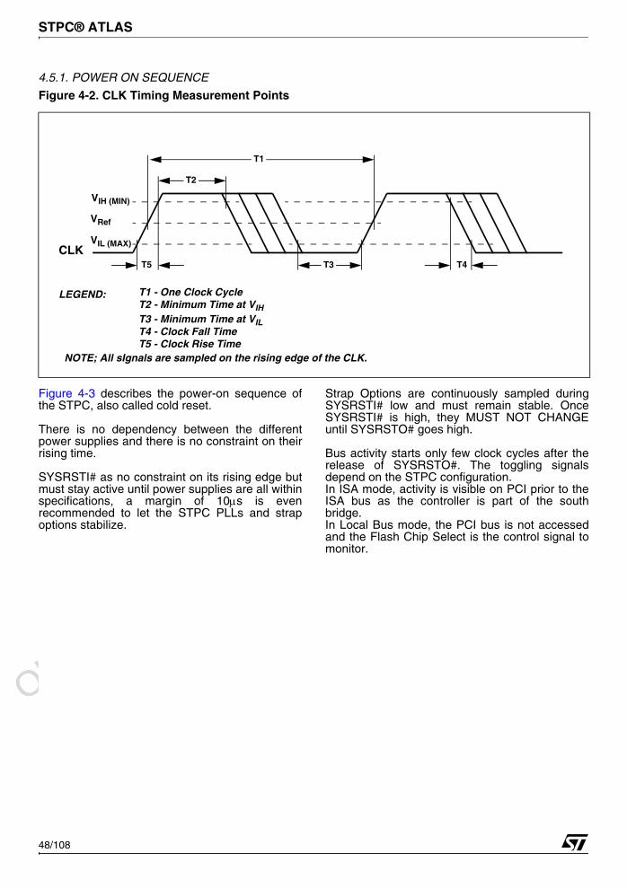
Obsolete Product(
s) - O
bsolete Product(
s)
Obsolete Product(
s) - O
bsolete Product(
s)
STPC® ATLAS
48/108
4.5.1. POWER ON SEQUENCE
Figure 4-3 describes the power-on sequence ofthe STPC, also called cold reset.
There is no dependency between the differentpower supplies and there is no constraint on theirrising time.
SYSRSTI# as no constraint on its rising edge butmust stay active until power supplies are all withinspecifications, a margin of 10µs is evenrecommended to let the STPC PLLs and strapoptions stabilize.
Strap Options are continuously sampled duringSYSRSTI# low and must remain stable. OnceSYSRSTI# is high, they MUST NOT CHANGEuntil SYSRSTO# goes high.
Bus activity starts only few clock cycles after therelease of SYSRSTO#. The toggling signalsdepend on the STPC configuration.In ISA mode, activity is visible on PCI prior to theISA bus as the controller is part of the southbridge.In Local Bus mode, the PCI bus is not accessedand the Flash Chip Select is the control signal tomonitor.
Figure 4-2. CLK Timing Measurement Points
CLKT5 T4T3
VRef
VIL (MAX)
VIH (MIN)
T2
T1
LEGEND: T1 - One Clock CycleT2 - Minimum Time at VIHT3 - Minimum Time at VILT4 - Clock Fall TimeT5 - Clock Rise Time
NOTE; All sIgnals are sampled on the rising edge of the CLK.
1
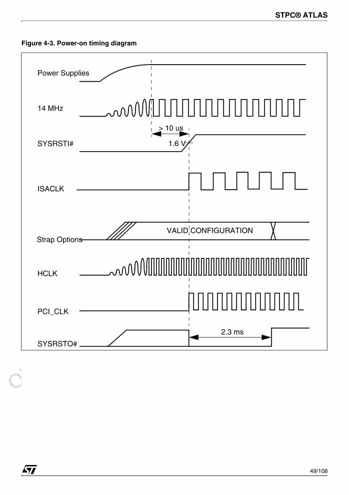
Obsolete Product(
s) - O
bsolete Product(
s)
Obsolete Product(
s) - O
bsolete Product(
s)
STPC® ATLAS
49/108
Figure 4-3. Power-on timing diagram
Strap Options
Power Supplies
SYSRSTI#
SYSRSTO#
14 MHz
1.6 V
VALID CONFIGURATION
> 10 us
HCLK
PCI_CLK
2.3 ms
ISACLK
1
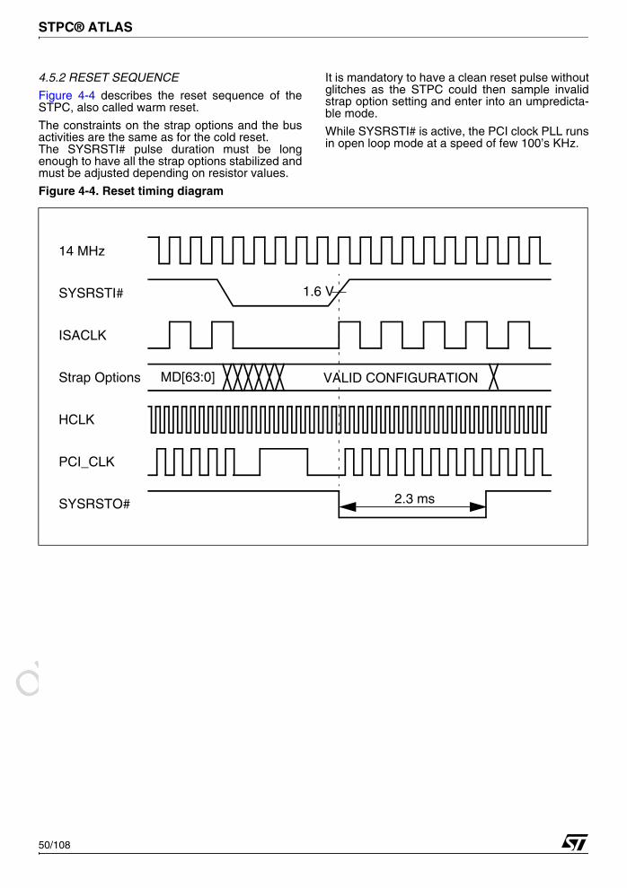
Obsolete Product(
s) - O
bsolete Product(
s)
Obsolete Product(
s) - O
bsolete Product(
s)
STPC® ATLAS
50/108
4.5.2 RESET SEQUENCE
Figure 4-4 describes the reset sequence of theSTPC, also called warm reset.
The constraints on the strap options and the busactivities are the same as for the cold reset.The SYSRSTI# pulse duration must be longenough to have all the strap options stabilized andmust be adjusted depending on resistor values.
It is mandatory to have a clean reset pulse withoutglitches as the STPC could then sample invalidstrap option setting and enter into an umpredicta-ble mode.
While SYSRSTI# is active, the PCI clock PLL runsin open loop mode at a speed of few 100’s KHz.
Figure 4-4. Reset timing diagram
Strap Options
SYSRSTI#
SYSRSTO#
14 MHz
VALID CONFIGURATION
HCLK
PCI_CLK
2.3 ms
ISACLK
1.6 V
MD[63:0]
1

Obsolete Product(
s) - O
bsolete Product(
s)
Obsolete Product(
s) - O
bsolete Product(
s)
STPC® ATLAS
51/108
4.5.3. SDRAM INTERFACE
Figure 4-5, Table 4-10, Table 4-11 lists the ACcharacteristics of the SDRAM interface. The
MCLKx clocks are the input clock of the SDRAMdevices.
The PC100 memory is recommended to reach 90MHz operation.
Figure 4-5. SDRAM Timing Diagram
Table 4-10. SDRAM Bus AC Timings - Commercial Temperature Range
Name Parameter Min Typ Max UnitTcycle MCLKI Cycle Time 11 nsThigh MCLKI High Time 4 nsTlow MCLKI Low Time 4 ns
MCLKI Rising Time 1 nsMCLKI Falling Time 1 ns
Tdelay MCLKx to MCLKI delay 0.5 1 1.5 ns
Toutput
MCLKI to RAS# Valid 1.6 5.2 nsMCLKI to CAS# Valid 1.6 5.2 nsMCLKI to CS# Valid 1.6 5.2 nsMCLKI to DQM[ ] Outputs Valid 1.35 5.2 nsMCLKI to MD[ ] Outputs Valid 1.35 5.2 nsMCLKI to MA[ ] Outputs Valid 1.6 5.2 nsMCLKI to MWE# Valid 1.6 5.2 ns
Tsetup MD[63:0] setup to MCKLI 4.7 nsThold MD[63:0] hold from MCKLI -0.36 2.3 ns
Note: These timings are for a load of 50pF, part running at 100MHz and ReadCLK activated and set to 0
MCLKI
STPC.output
STPC.input
MCLKx Tdelay
TsetupThold
Toutput (min)Toutput (max)
Tcycle
Thigh Tlow
1
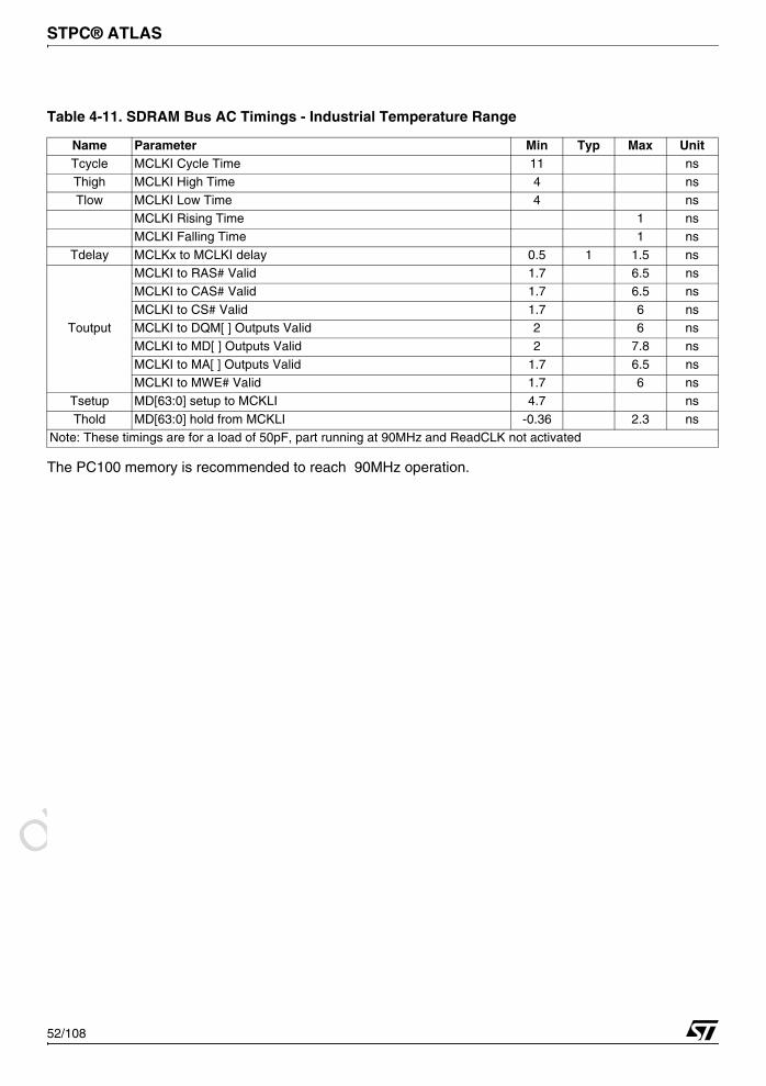
Obsolete Product(
s) - O
bsolete Product(
s)
Obsolete Product(
s) - O
bsolete Product(
s)
STPC® ATLAS
52/108
The PC100 memory is recommended to reach 90MHz operation.
Table 4-11. SDRAM Bus AC Timings - Industrial Temperature Range
Name Parameter Min Typ Max UnitTcycle MCLKI Cycle Time 11 nsThigh MCLKI High Time 4 nsTlow MCLKI Low Time 4 ns
MCLKI Rising Time 1 nsMCLKI Falling Time 1 ns
Tdelay MCLKx to MCLKI delay 0.5 1 1.5 ns
Toutput
MCLKI to RAS# Valid 1.7 6.5 nsMCLKI to CAS# Valid 1.7 6.5 nsMCLKI to CS# Valid 1.7 6 nsMCLKI to DQM[ ] Outputs Valid 2 6 nsMCLKI to MD[ ] Outputs Valid 2 7.8 nsMCLKI to MA[ ] Outputs Valid 1.7 6.5 nsMCLKI to MWE# Valid 1.7 6 ns
Tsetup MD[63:0] setup to MCKLI 4.7 nsThold MD[63:0] hold from MCKLI -0.36 2.3 ns
Note: These timings are for a load of 50pF, part running at 90MHz and ReadCLK not activated
1
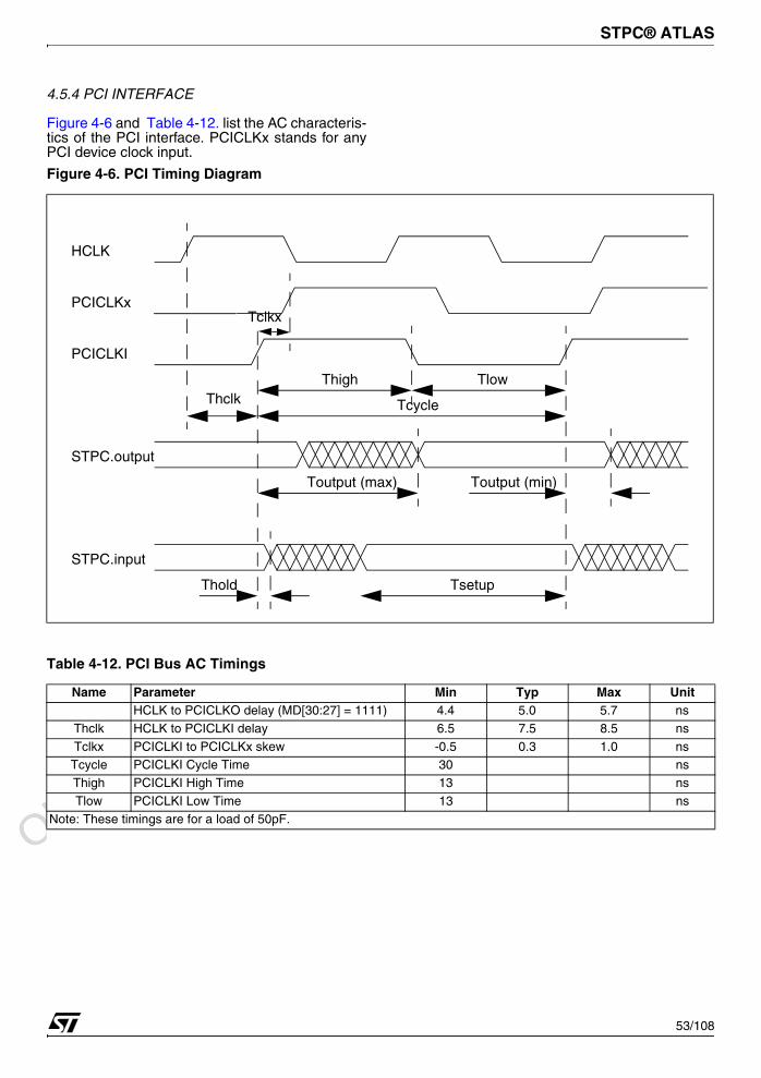
Obsolete Product(
s) - O
bsolete Product(
s)
Obsolete Product(
s) - O
bsolete Product(
s)
STPC® ATLAS
53/108
4.5.4 PCI INTERFACE
Figure 4-6 and Table 4-12. list the AC characteris-tics of the PCI interface. PCICLKx stands for anyPCI device clock input.
Figure 4-6. PCI Timing Diagram
PCICLKI
STPC.output
STPC.input
PCICLKx
TsetupThold
Toutput (min)Toutput (max)
Tcycle
Thigh Tlow
HCLK
Thclk
Tclkx
Table 4-12. PCI Bus AC Timings
Name Parameter Min Typ Max UnitHCLK to PCICLKO delay (MD[30:27] = 1111) 4.4 5.0 5.7 ns
Thclk HCLK to PCICLKI delay 6.5 7.5 8.5 nsTclkx PCICLKI to PCICLKx skew -0.5 0.3 1.0 nsTcycle PCICLKI Cycle Time 30 nsThigh PCICLKI High Time 13 nsTlow PCICLKI Low Time 13 ns
Note: These timings are for a load of 50pF.
1

Obsolete Product(
s) - O
bsolete Product(
s)
Obsolete Product(
s) - O
bsolete Product(
s)
STPC® ATLAS
54/108
4.5.5 IPC INTERFACE
Table 4-13 lists the AC characteristics of the IPCinterface.
Figure 4-7. IPC timing diagram
ISACLK
IRQ_MUX[3:0]
DREQ_MUX[1:0]
ISACLK2X Tdly
TsetupTsetup
Table 4-13. IPC Interface AC Timings
Name Parameter Min Max UnitTsetup IRQ_MUX[3:0] Input setup to ISACLK2X 0 - nSTsetup DREQ_MUX[1:0] Input setup to ISACLK2X 0 - nS
1
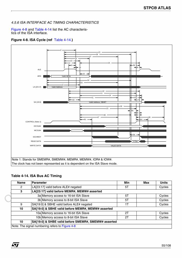
Obsolete Product(
s) - O
bsolete Product(
s)
Obsolete Product(
s) - O
bsolete Product(
s)
STPC® ATLAS
55/108
4.5.6 ISA INTERFACE AC TIMING CHARACTERISTICS
Figure 4-8 and Table 4-14 list the AC characteris-tics of the ISA interface.
Figure 4-8. ISA Cycle (ref Table 4-14.)
Note 1: Stands for SMEMR#, SMEMW#, MEMR#, MEMW#, IOR# & IOW#.The clock has not been represented as it is dependent on the ISA Slave mode.
Valid AENx
Valid Address
Valid Address, SBHE*
V.Data
VALID DATA
54
28
26
64
5958
55
28
23
61
4847
2623
5727
24
42
4110
11
3433
3
22
5629
259
18
2
12
3837
15
1413
12
ALE
AEN
LA [23:17]
SA [19:0]
CONTROL (Note 1)
IOCS16#
MCS16#
IOCHRDY
READ DATA
WRITE DATA
Table 4-14. ISA Bus AC Timing
Name Parameter Min Max Units2 LA[23:17] valid before ALE# negated 5T Cycles3 LA[23:17] valid before MEMR#, MEMW# asserted
3a Memory access to 16-bit ISA Slave 5T Cycles3b Memory access to 8-bit ISA Slave 5T Cycles
9 SA[19:0] & SBHE valid before ALE# negated 1T Cycles10 SA[19:0] & SBHE valid before MEMR#, MEMW# asserted
10a Memory access to 16-bit ISA Slave 2T Cycles10b Memory access to 8-bit ISA Slave 2T Cycles
10 SA[19:0] & SHBE valid before SMEMR#, SMEMW# assertedNote: The signal numbering refers to Figure 4-8
1

Obsolete Product(
s) - O
bsolete Product(
s)
Obsolete Product(
s) - O
bsolete Product(
s)
STPC® ATLAS
56/108
10c Memory access to 16-bit ISA Slave 2T Cycle10d Memory access to 8-bit ISA Slave 2T Cycle
10e SA[19:0] & SBHE valid before IOR#, IOW# asserted 2T Cycles11 ISACLK2X to IOW# valid
11a Memory access to 16-bit ISA Slave - 2BCLK 2T Cycles11b Memory access to 16-bit ISA Slave - Standard 3BCLK 2T Cycles11c Memory access to 16-bit ISA Slave - 4BCLK 2T Cycles11d Memory access to 8-bit ISA Slave - 2BCLK 2T Cycles
11e Memory access to 8-bit ISA Slave - Standard 3BCLK 2T Cycles12 ALE# asserted before ALE# negated 1T Cycles13 ALE# asserted before MEMR#, MEMW# asserted
13a Memory Access to 16-bit ISA Slave 2T Cycles13b Memory Access to 8-bit ISA Slave 2T Cycles
13 ALE# asserted before SMEMR#, SMEMW# asserted13c Memory Access to 16-bit ISA Slave 2T Cycles13d Memory Access to 8-bit ISA Slave 2T Cycles
13e ALE# asserted before IOR#, IOW# asserted 2T Cycles14 ALE# asserted before AL[23:17]
14a Non compressed 15T Cycles14b Compressed 15T Cycles
15 ALE# asserted before MEMR#, MEMW#, SMEMR#, SMEMW# negated15a Memory Access to 16-bit ISA Slave- 4 BCLK 11T Cycles15e Memory Access to 8-bit ISA Slave- Standard Cycle 11T Cycles
18a ALE# negated before LA[23:17] invalid (non compressed) 14T Cycles18a ALE# negated before LA[23:17] invalid (compressed) 14T Cycles22 MEMR#, MEMW# asserted before LA[23:17]
22a Memory access to 16-bit ISA Slave. 13T Cycles22b Memory access to 8-bit ISA Slave. 13T Cycles
23 MEMR#, MEMW# asserted before MEMR#, MEMW# negated23b Memory access to 16-bit ISA Slave Standard cycle 9T Cycles23e Memory access to 8-bit ISA Slave Standard cycle 9T Cycles
23 SMEMR#, SMEMW# asserted before SMEMR#, SMEMW# negated23h Memory access to 16-bit ISA Slave Standard cycle 9T Cycles23l Memory access to 16-bit ISA Slave Standard cycle 9T Cycles
23 IOR#, IOW# asserted before IOR#, IOW# negated23o Memory access to 16-bit ISA Slave Standard cycle 9T Cycles23r Memory access to 8-bit ISA Slave Standard cycle 9T Cycles
24 MEMR#, MEMW# asserted before SA[19:0]24b Memory access to 16-bit ISA Slave Standard cycle 10T Cycles24d Memory access to 8-bit ISA Slave - 3BLCK 10T Cycles24e Memory access to 8-bit ISA Slave Standard cycle 10T Cycles24f Memory access to 8-bit ISA Slave - 7BCLK 10T Cycles
24 SMEMR#, SMEMW# asserted before SA[19:0]24h Memory access to 16-bit ISA Slave Standard cycle 10T Cycles
Table 4-14. ISA Bus AC Timing
Name Parameter Min Max Units
Note: The signal numbering refers to Figure 4-8
1
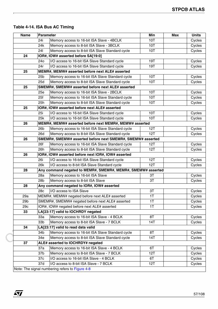
Obsolete Product(
s) - O
bsolete Product(
s)
Obsolete Product(
s) - O
bsolete Product(
s)
STPC® ATLAS
57/108
24i Memory access to 16-bit ISA Slave - 4BCLK 10T Cycles24k Memory access to 8-bit ISA Slave - 3BCLK 10T Cycles24l Memory access to 8-bit ISA Slave Standard cycle 10T Cycles
24 IOR#, IOW# asserted before SA[19:0]24o I/O access to 16-bit ISA Slave Standard cycle 19T Cycles24r I/O access to 16-bit ISA Slave Standard cycle 19T Cycles
25 MEMR#, MEMW# asserted before next ALE# asserted25b Memory access to 16-bit ISA Slave Standard cycle 10T Cycles25d Memory access to 8-bit ISA Slave Standard cycle 10T Cycles
25 SMEMR#, SMEMW# asserted before next ALE# asserted25e Memory access to 16-bit ISA Slave - 2BCLK 10T Cycles25f Memory access to 16-bit ISA Slave Standard cycle 10T Cycles25h Memory access to 8-bit ISA Slave Standard cycle 10T Cycles
25 IOR#, IOW# asserted before next ALE# asserted25i I/O access to 16-bit ISA Slave Standard cycle 10T Cycles25k I/O access to 16-bit ISA Slave Standard cycle 10T Cycles
26 MEMR#, MEMW# asserted before next MEMR#, MEMW# asserted26b Memory access to 16-bit ISA Slave Standard cycle 12T Cycles26d Memory access to 8-bit ISA Slave Standard cycle 12T Cycles
26 SMEMR#, SMEMW# asserted before next SMEMR#, SMEMW# asserted26f Memory access to 16-bit ISA Slave Standard cycle 12T Cycles26h Memory access to 8-bit ISA Slave Standard cycle 12T Cycles
26 IOR#, IOW# asserted before next IOR#, IOW# asserted26i I/O access to 16-bit ISA Slave Standard cycle 12T Cycles26k I/O access to 8-bit ISA Slave Standard cycle 12T Cycles
28 Any command negated to MEMR#, SMEMR#, MEMR#, SMEMW# asserted28a Memory access to 16-bit ISA Slave 3T Cycles28b Memory access to 8-bit ISA Slave 3T Cycles
28 Any command negated to IOR#, IOW# asserted28c I/O access to ISA Slave 3T Cycles
29a MEMR#, MEMW# negated before next ALE# asserted 1T Cycles29b SMEMR#, SMEMW# negated before next ALE# asserted 1T Cycles29c IOR#, IOW# negated before next ALE# asserted 1T Cycles33 LA[23:17] valid to IOCHRDY negated
33a Memory access to 16-bit ISA Slave - 4 BCLK 8T Cycles33b Memory access to 8-bit ISA Slave - 7 BCLK 14T Cycles
34 LA[23:17] valid to read data valid34b Memory access to 16-bit ISA Slave Standard cycle 8T Cycles34e Memory access to 8-bit ISA Slave Standard cycle 14T Cycles
37 ALE# asserted to IOCHRDY# negated37a Memory access to 16-bit ISA Slave - 4 BCLK 6T Cycles37b Memory access to 8-bit ISA Slave - 7 BCLK 12T Cycles37c I/O access to 16-bit ISA Slave - 4 BCLK 6T Cycles37d I/O access to 8-bit ISA Slave - 7 BCLK 12T Cycles
Table 4-14. ISA Bus AC Timing
Name Parameter Min Max Units
Note: The signal numbering refers to Figure 4-8
1
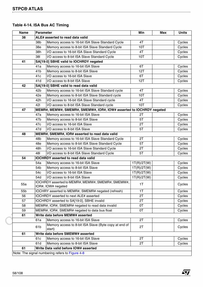
Obsolete Product(
s) - O
bsolete Product(
s)
Obsolete Product(
s) - O
bsolete Product(
s)
STPC® ATLAS
58/108
38 ALE# asserted to read data valid38b Memory access to 16-bit ISA Slave Standard Cycle 4T Cycles38e Memory access to 8-bit ISA Slave Standard Cycle 10T Cycles38h I/O access to 16-bit ISA Slave Standard Cycle 4T Cycles38l I/O access to 8-bit ISA Slave Standard Cycle 10T Cycles
41 SA[19:0] SBHE valid to IOCHRDY negated41a Memory access to 16-bit ISA Slave 6T Cycles41b Memory access to 8-bit ISA Slave 12T Cycles41c I/O access to 16-bit ISA Slave 6T Cycles41d I/O access to 8-bit ISA Slave 12T Cycles
42 SA[19:0] SBHE valid to read data valid42b Memory access to 16-bit ISA Slave Standard cycle 4T Cycles42e Memory access to 8-bit ISA Slave Standard cycle 10T Cycles42h I/O access to 16-bit ISA Slave Standard cycle 4T Cycles42l I/O access to 8-bit ISA Slave Standard cycle 10T Cycles
47 MEMR#, MEMW#, SMEMR#, SMEMW#, IOR#, IOW# asserted to IOCHRDY negated47a Memory access to 16-bit ISA Slave 2T Cycles47b Memory access to 8-bit ISA Slave 5T Cycles47c I/O access to 16-bit ISA Slave 2T Cycles47d I/O access to 8-bit ISA Slave 5T Cycles
48 MEMR#, SMEMR#, IOR# asserted to read data valid48b Memory access to 16-bit ISA Slave Standard Cycle 2T Cycles48e Memory access to 8-bit ISA Slave Standard Cycle 5T Cycles48h I/O access to 16-bit ISA Slave Standard Cycle 2T Cycles48l I/O access to 8-bit ISA Slave Standard Cycle 5T Cycles
54 IOCHRDY asserted to read data valid54a Memory access to 16-bit ISA Slave 1T(R)/2T(W) Cycles54b Memory access to 8-bit ISA Slave 1T(R)/2T(W) Cycles54c I/O access to 16-bit ISA Slave 1T(R)/2T(W) Cycles54d I/O access to 8-bit ISA Slave 1T(R)/2T(W) Cycles
55aIOCHRDY asserted to MEMR#, MEMW#, SMEMR#, SMEMW#, IOR#, IOW# negated
1T Cycles
55b IOCHRY asserted to MEMR#, SMEMR# negated (refresh) 1T Cycles56 IOCHRDY asserted to next ALE# asserted 2T Cycles57 IOCHRDY asserted to SA[19:0], SBHE invalid 2T Cycles58 MEMR#, IOR#, SMEMR# negated to read data invalid 0T Cycles59 MEMR#, IOR#, SMEMR# negated to data bus float 0T Cycles61 Write data before MEMW# asserted
61a Memory access to 16-bit ISA Slave 2T Cycles
61bMemory access to 8-bit ISA Slave (Byte copy at end of start)
2T Cycles
61 Write data before SMEMW# asserted61c Memory access to 16-bit ISA Slave 2T Cycles61d Memory access to 8-bit ISA Slave 2T Cycles
61 Write Data valid before IOW# asserted
Table 4-14. ISA Bus AC Timing
Name Parameter Min Max Units
Note: The signal numbering refers to Figure 4-8
1
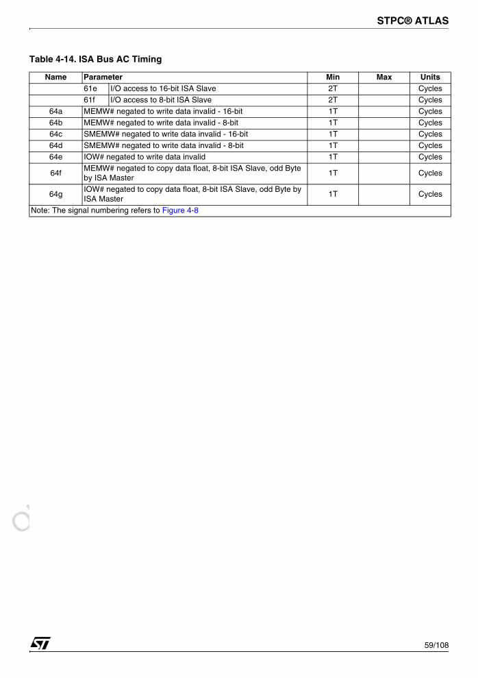
Obsolete Product(
s) - O
bsolete Product(
s)
Obsolete Product(
s) - O
bsolete Product(
s)
STPC® ATLAS
59/108
61e I/O access to 16-bit ISA Slave 2T Cycles61f I/O access to 8-bit ISA Slave 2T Cycles
64a MEMW# negated to write data invalid - 16-bit 1T Cycles64b MEMW# negated to write data invalid - 8-bit 1T Cycles64c SMEMW# negated to write data invalid - 16-bit 1T Cycles64d SMEMW# negated to write data invalid - 8-bit 1T Cycles64e IOW# negated to write data invalid 1T Cycles
64fMEMW# negated to copy data float, 8-bit ISA Slave, odd Byte by ISA Master
1T Cycles
64gIOW# negated to copy data float, 8-bit ISA Slave, odd Byte by ISA Master
1T Cycles
Table 4-14. ISA Bus AC Timing
Name Parameter Min Max Units
Note: The signal numbering refers to Figure 4-8
1
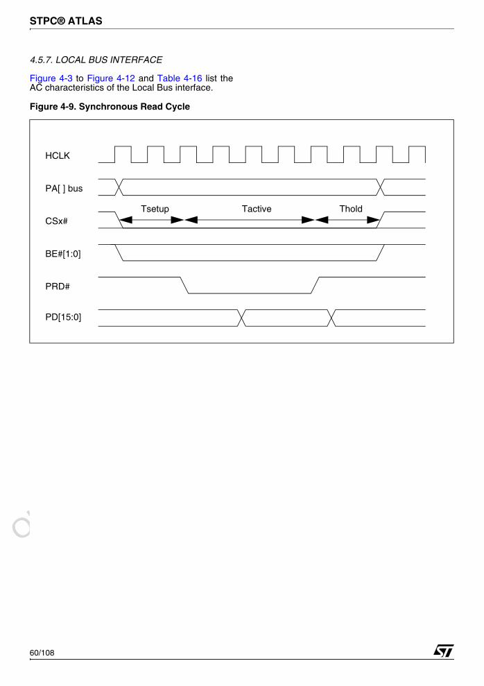
Obsolete Product(
s) - O
bsolete Product(
s)
Obsolete Product(
s) - O
bsolete Product(
s)
STPC® ATLAS
60/108
4.5.7. LOCAL BUS INTERFACE
Figure 4-3 to Figure 4-12 and Table 4-16 list theAC characteristics of the Local Bus interface.
Figure 4-9. Synchronous Read Cycle
PA[ ] bus
CSx#
BE#[1:0]
PRD#
HCLK
Tsetup Tactive Thold
PD[15:0]
1
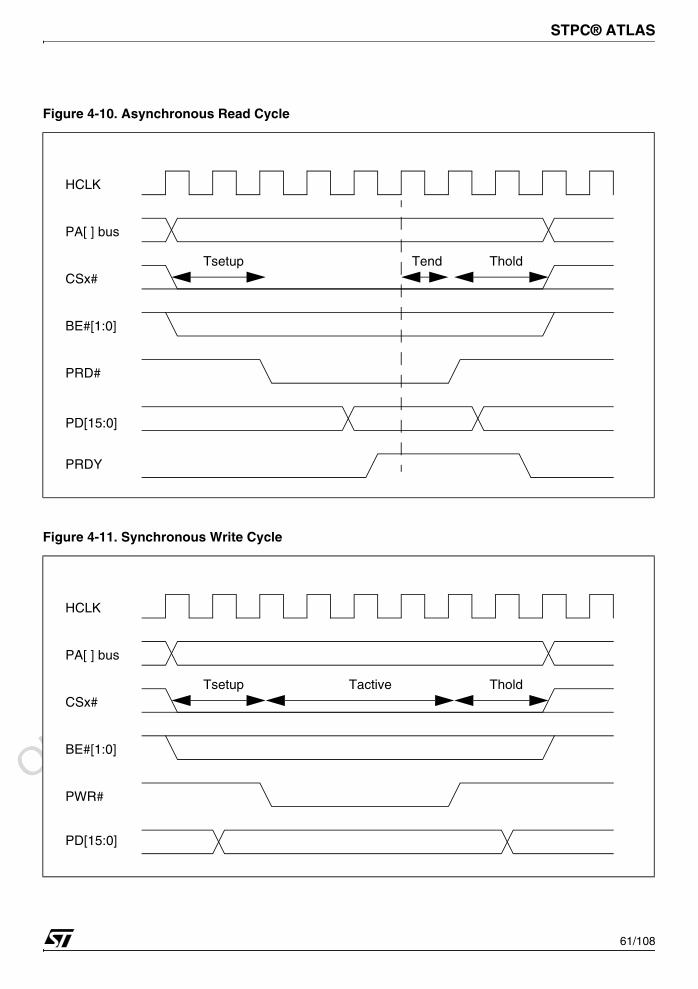
Obsolete Product(
s) - O
bsolete Product(
s)
Obsolete Product(
s) - O
bsolete Product(
s)
STPC® ATLAS
61/108
Figure 4-10. Asynchronous Read Cycle
Figure 4-11. Synchronous Write Cycle
PA[ ] bus
CSx#
BE#[1:0]
PRD#
HCLK
Tsetup Tend Thold
PD[15:0]
PRDY
PA[ ] bus
CSx#
BE#[1:0]
PWR#
HCLK
Tsetup Tactive Thold
PD[15:0]
1

Obsolete Product(
s) - O
bsolete Product(
s)
Obsolete Product(
s) - O
bsolete Product(
s)
STPC® ATLAS
62/108
The Table 4-15. below refers to Vh, Va, Vs whichare the register value for Setup time, Active Time
and Hold time, as described in the ProgrammingManual.
Figure 4-12. Asynchronous Write Cycle
PA[ ] bus
CSx#
BE#[1:0]
PWR#
HCLK
Tsetup Tend Thold
PRDY
PD[15:0]
Table 4-15. Local Bus cycle lenght
Cycle Tsetup Tactive Thold Tend UnitMemory (FCSx#) 4 + Vh 2 + Va 4 + Vs 4 HCLKPeripheral (IOCSx#) 4 + Vh 2 + Va 4 + Vs 4 HCLK
Table 4-16. Local Bus Interface AC Timing
Name Parameters Min Max UnitsHCLK to PA bus - 15 nSHCLK to PD bus - 15 nSHCLK to FCS#[1:0] - 15 nSHCLK to IOCS#[3:0] - 15 nSHCLK to PWR#, PRD# - 15 nSHCLK to BE#[1:0] - 15 nSPD[15:0] Input setup to HCLK - 4 nSPD[15:0] Input hold to HCLK 2 - nSPRDY Input setup to HCLK - 4 nSPRDY Input hold to HCLK 2 - nS
1
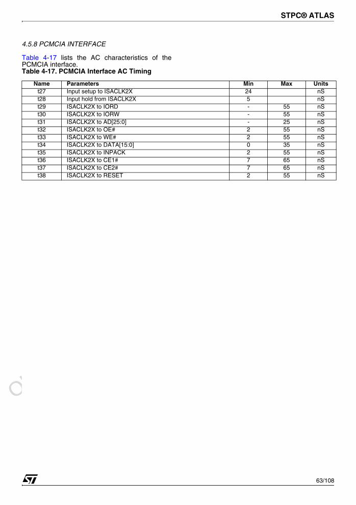
Obsolete Product(
s) - O
bsolete Product(
s)
Obsolete Product(
s) - O
bsolete Product(
s)
STPC® ATLAS
63/108
4.5.8 PCMCIA INTERFACE
Table 4-17 lists the AC characteristics of thePCMCIA interface.Table 4-17. PCMCIA Interface AC Timing
Name Parameters Min Max Unitst27 Input setup to ISACLK2X 24 nSt28 Input hold from ISACLK2X 5 nSt29 ISACLK2X to IORD - 55 nSt30 ISACLK2X to IORW - 55 nSt31 ISACLK2X to AD[25:0] - 25 nSt32 ISACLK2X to OE# 2 55 nSt33 ISACLK2X to WE# 2 55 nSt34 ISACLK2X to DATA[15:0] 0 35 nSt35 ISACLK2X to INPACK 2 55 nSt36 ISACLK2X to CE1# 7 65 nSt37 ISACLK2X to CE2# 7 65 nSt38 ISACLK2X to RESET 2 55 nS
1
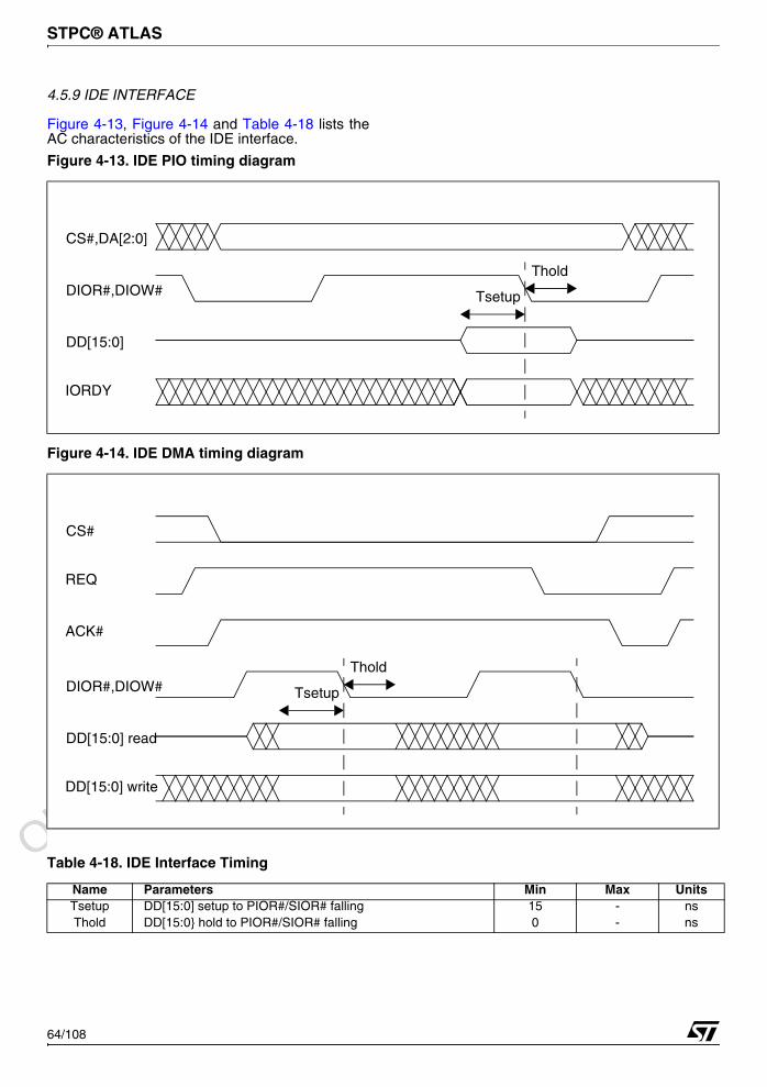
Obsolete Product(
s) - O
bsolete Product(
s)
Obsolete Product(
s) - O
bsolete Product(
s)
STPC® ATLAS
64/108
4.5.9 IDE INTERFACE
Figure 4-13, Figure 4-14 and Table 4-18 lists theAC characteristics of the IDE interface.
Figure 4-13. IDE PIO timing diagram
Figure 4-14. IDE DMA timing diagram
DIOR#,DIOW#
CS#,DA[2:0]
DD[15:0]
Thold
IORDY
Tsetup
DIOR#,DIOW#
CS#
DD[15:0] read
DD[15:0] write
REQ
ACK#
Thold
Tsetup
Table 4-18. IDE Interface Timing
Name Parameters Min Max UnitsTsetup DD[15:0] setup to PIOR#/SIOR# falling 15 - nsThold DD[15:0 hold to PIOR#/SIOR# falling 0 - ns
1
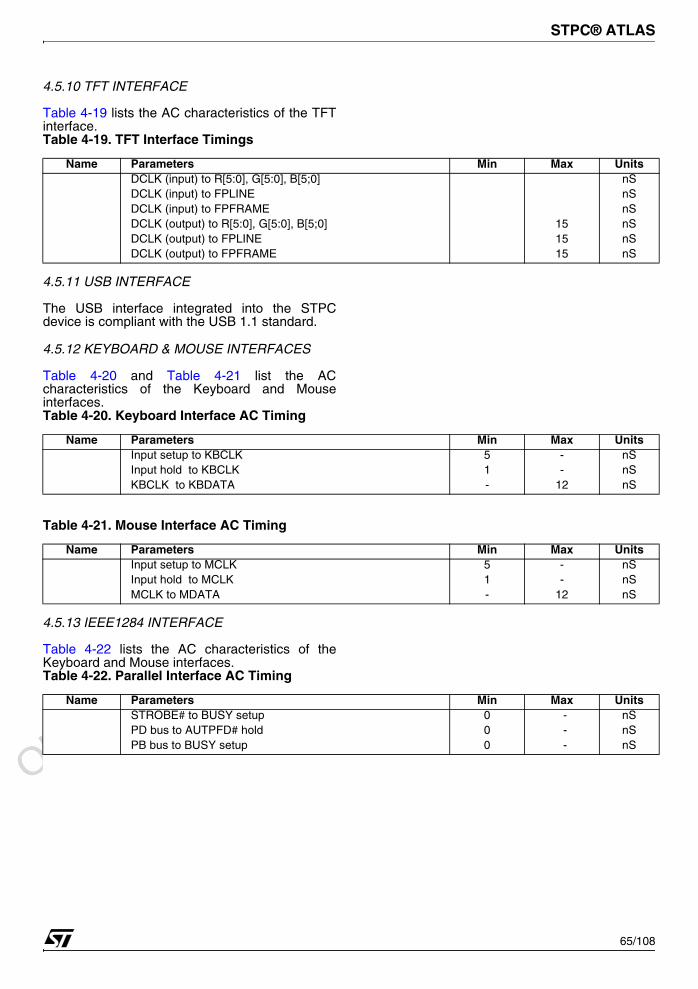
Obsolete Product(
s) - O
bsolete Product(
s)
Obsolete Product(
s) - O
bsolete Product(
s)
STPC® ATLAS
65/108
4.5.10 TFT INTERFACE
Table 4-19 lists the AC characteristics of the TFTinterface.
4.5.11 USB INTERFACE
The USB interface integrated into the STPCdevice is compliant with the USB 1.1 standard.
4.5.12 KEYBOARD & MOUSE INTERFACES
Table 4-20 and Table 4-21 list the ACcharacteristics of the Keyboard and Mouseinterfaces.
4.5.13 IEEE1284 INTERFACE
Table 4-22 lists the AC characteristics of theKeyboard and Mouse interfaces.
Table 4-19. TFT Interface Timings
Name Parameters Min Max UnitsDCLK (input) to R[5:0], G[5:0], B[5;0] nSDCLK (input) to FPLINE nSDCLK (input) to FPFRAME nSDCLK (output) to R[5:0], G[5:0], B[5;0] 15 nSDCLK (output) to FPLINE 15 nSDCLK (output) to FPFRAME 15 nS
Table 4-20. Keyboard Interface AC Timing
Name Parameters Min Max UnitsInput setup to KBCLK 5 - nSInput hold to KBCLK 1 - nSKBCLK to KBDATA - 12 nS
Table 4-21. Mouse Interface AC Timing
Name Parameters Min Max UnitsInput setup to MCLK 5 - nSInput hold to MCLK 1 - nSMCLK to MDATA - 12 nS
Table 4-22. Parallel Interface AC Timing
Name Parameters Min Max UnitsSTROBE# to BUSY setup 0 - nSPD bus to AUTPFD# hold 0 - nSPB bus to BUSY setup 0 - nS
1
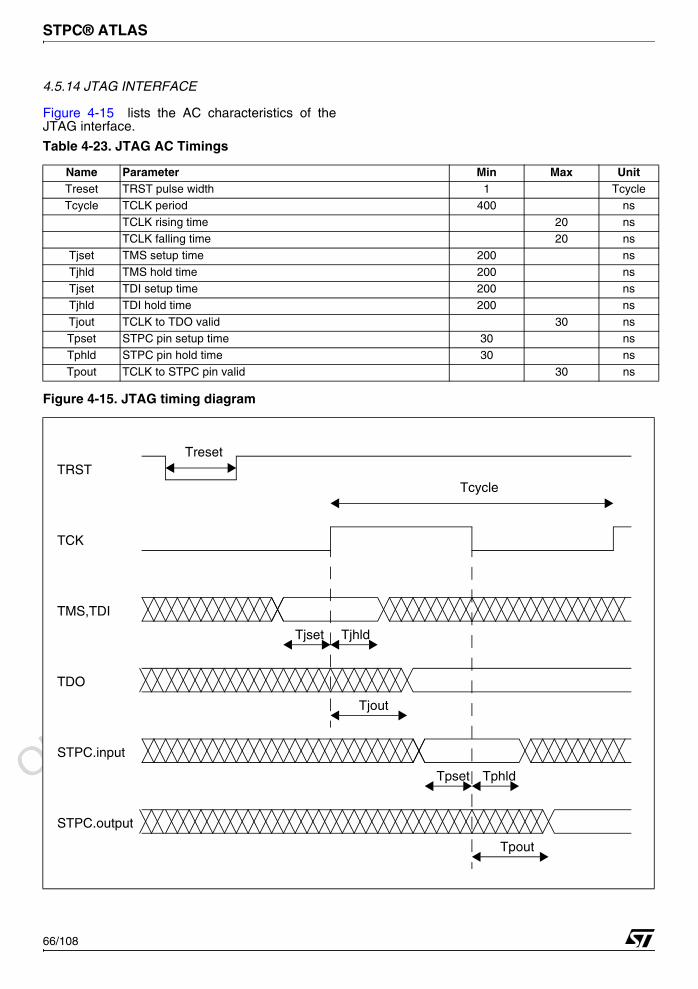
Obsolete Product(
s) - O
bsolete Product(
s)
Obsolete Product(
s) - O
bsolete Product(
s)
STPC® ATLAS
66/108
4.5.14 JTAG INTERFACE
Figure 4-15 lists the AC characteristics of theJTAG interface.
Table 4-23. JTAG AC Timings
Name Parameter Min Max UnitTreset TRST pulse width 1 TcycleTcycle TCLK period 400 ns
TCLK rising time 20 nsTCLK falling time 20 ns
Tjset TMS setup time 200 nsTjhld TMS hold time 200 nsTjset TDI setup time 200 nsTjhld TDI hold time 200 nsTjout TCLK to TDO valid 30 nsTpset STPC pin setup time 30 nsTphld STPC pin hold time 30 nsTpout TCLK to STPC pin valid 30 ns
Figure 4-15. JTAG timing diagram
TCK
STPC.input
TRSTTreset
Tcycle
STPC.output
TMS,TDI
TDO
Tjset Tjhld
Tjout
Tpset Tphld
Tpout
1
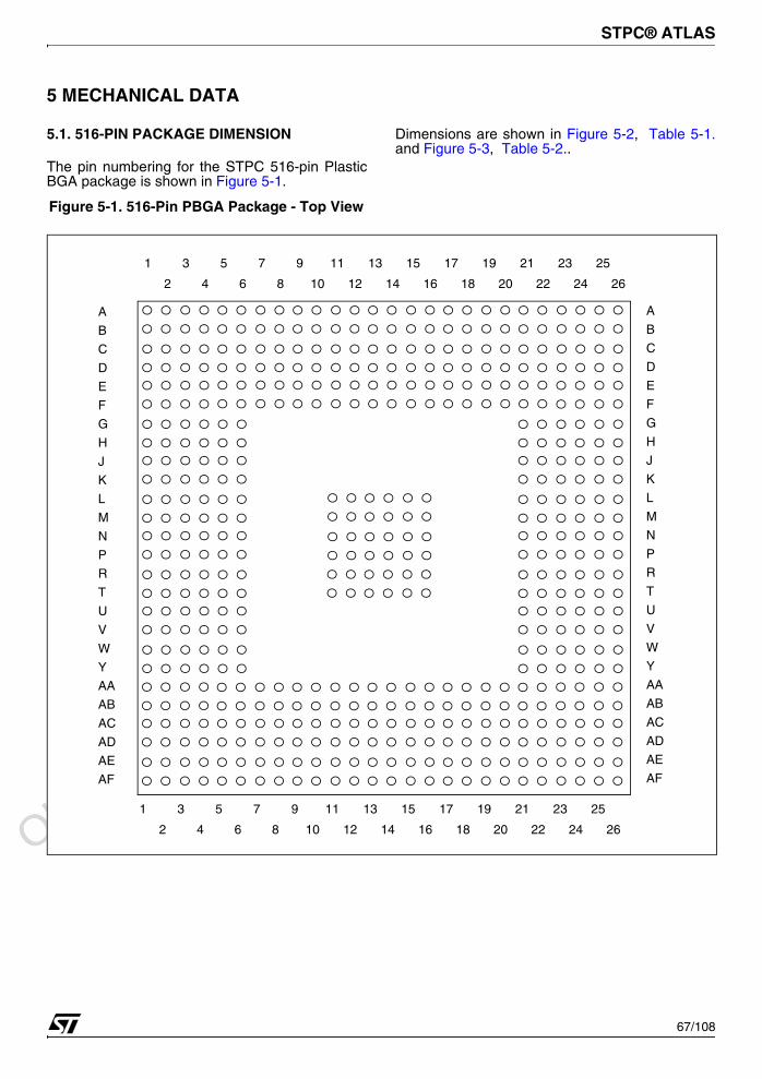
Obsolete Product(
s) - O
bsolete Product(
s)
Obsolete Product(
s) - O
bsolete Product(
s)
STPC® ATLAS
67/108
5 MECHANICAL DATA
5.1. 516-PIN PACKAGE DIMENSION
The pin numbering for the STPC 516-pin PlasticBGA package is shown in Figure 5-1.
Dimensions are shown in Figure 5-2, Table 5-1.and Figure 5-3, Table 5-2..
Figure 5-1. 516-Pin PBGA Package - Top View
A
B
D
E
F
G
H
J
K
L
M
N
P
R
T
U
V
W
Y
AA
AB
AC
AD
AE
AF
C
1 3 5 7 9 11 13 15 17 19 21 23 25
2 4 6 8 10 12 14 16 18 20 22 24 26
A
B
D
E
F
G
H
J
K
L
M
N
P
R
T
U
V
W
Y
AA
AB
AC
AD
AE
AF
C
1 3 5 7 9 11 13 15 17 19 21 23 25
2 4 6 8 10 12 14 16 18 20 22 24 26
1
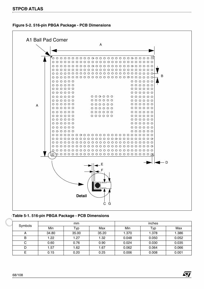
Obsolete Product(
s) - O
bsolete Product(
s)
Obsolete Product(
s) - O
bsolete Product(
s)
STPC® ATLAS
68/108
Figure 5-2. 516-pin PBGA Package - PCB Dimensions
Table 5-1. 516-pin PBGA Package - PCB Dimensions
Symbolsmm inches
Min Typ Max Min Typ MaxA 34.80 35.00 35.20 1.370 1.378 1.386B 1.22 1.27 1.32 0.048 0.050 0.052C 0.60 0.76 0.90 0.024 0.030 0.035D 1.57 1.62 1.67 0.062 0.064 0.066E 0.15 0.20 0.25 0.006 0.008 0.001
A
A
B
Detail
A1 Ball Pad Corner
D
F
E
GC
1
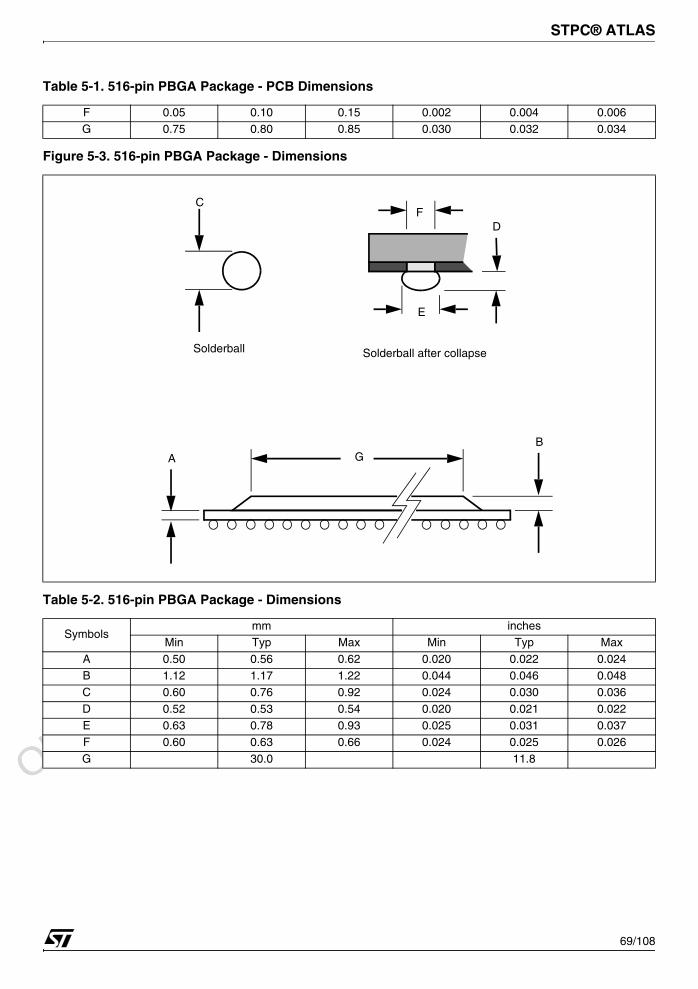
Obsolete Product(
s) - O
bsolete Product(
s)
Obsolete Product(
s) - O
bsolete Product(
s)
STPC® ATLAS
69/108
F 0.05 0.10 0.15 0.002 0.004 0.006G 0.75 0.80 0.85 0.030 0.032 0.034
Figure 5-3. 516-pin PBGA Package - Dimensions
Table 5-2. 516-pin PBGA Package - Dimensions
Symbolsmm inches
Min Typ Max Min Typ MaxA 0.50 0.56 0.62 0.020 0.022 0.024B 1.12 1.17 1.22 0.044 0.046 0.048C 0.60 0.76 0.92 0.024 0.030 0.036D 0.52 0.53 0.54 0.020 0.021 0.022E 0.63 0.78 0.93 0.025 0.031 0.037F 0.60 0.63 0.66 0.024 0.025 0.026G 30.0 11.8
Table 5-1. 516-pin PBGA Package - PCB Dimensions
AB
C
Solderball Solderball after collapse
D
E
F
G
1
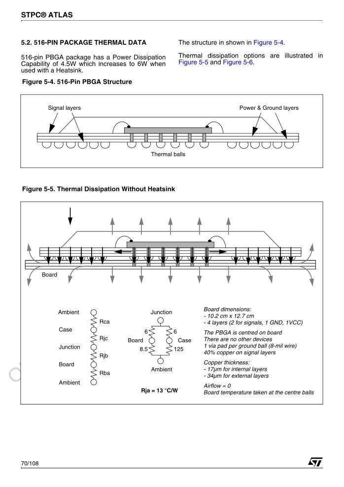
Obsolete Product(
s) - O
bsolete Product(
s)
Obsolete Product(
s) - O
bsolete Product(
s)
STPC® ATLAS
70/108
5.2. 516-PIN PACKAGE THERMAL DATA
516-pin PBGA package has a Power DissipationCapability of 4.5W which increases to 6W whenused with a Heatsink.
The structure in shown in Figure 5-4.
Thermal dissipation options are illustrated inFigure 5-5 and Figure 5-6.
Figure 5-4. 516-Pin PBGA Structure
Thermal balls
Power & Ground layersSignal layers
Figure 5-5. Thermal Dissipation Without Heatsink
Ambient
Case
Junction
Board
Ambient
Ambient
Case
Junction
Board
Rca
Rjc
Rjb
Rba
6 6
1258.5
Rja = 13 °C/WAirflow = 0
Board dimensions:
The PBGA is centred on board
Copper thickness:- 17µm for internal layers- 34µm for external layers
- 10.2 cm x 12.7 cm- 4 layers (2 for signals, 1 GND, 1VCC)
There are no other devices1 via pad per ground ball (8-mil wire)40% copper on signal layers
Board temperature taken at the centre balls
Board
1

Obsolete Product(
s) - O
bsolete Product(
s)
Obsolete Product(
s) - O
bsolete Product(
s)
STPC® ATLAS
71/108
Figure 5-6. Thermal Dissipation With Heatsink
Ambient
Case
Junction
Board
Ambient
Ambient
Case
Junction
Board
Rca
Rjc
Rjb
Rba
3 6
508.5
Rja = 9.5 °C/WAirflow = 0
Board dimensions:
The PBGA is centred on board
Copper thickness:- 17µm for internal layers- 34µm for external layers
- 10.2 cm x 12.7 cm- 4 layers (2 for signals, 1 GND, 1VCC)
There are no other devices
Heat sink is 11.1°C/W
1 via pad per ground ball (8-mil wire)40% copper on signal layers
Board temperature taken at the centre balls
Board
1
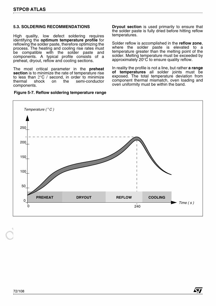
Obsolete Product(
s) - O
bsolete Product(
s)
Obsolete Product(
s) - O
bsolete Product(
s)
STPC® ATLAS
72/108
5.3. SOLDERING RECOMMENDATIONS
High quality, low defect soldering requiresidentifying the optimum temperature profile forreflowing the solder paste, therefore optimizing theprocess. The heating and cooling rise rates mustbe compatible with the solder paste andcomponents. A typical profile consists of apreheat, dryout, reflow and cooling sections.
The most critical parameter in the preheatsection is to minimize the rate of temperature riseto less than 2°C / second, in order to minimizethermal shock on the semi-conductorcomponents.
Dryout section is used primarily to ensure thatthe solder paste is fully dried before hitting reflowtemperatures.
Solder reflow is accomplished in the reflow zone,where the solder paste is elevated to atemperature greater than the melting point of thesolder. Melting temperature must be exceeded byapproximately 20°C to ensure quality reflow.
In reality the profile is not a line, but rather a rangeof temperatures all solder joints must beexposed. The total temperature deviation fromcomponent thermal mismatch, oven loading andoven uniformity must be within the band.
Figure 5-7. Reflow soldering temperature range
Temperature ( °C )
Time ( s )
PREHEAT DRYOUT REFLOW COOLING
240
0
250
200
150
100
50
0
1

Obsolete Product(
s) - O
bsolete Product(
s)
Obsolete Product(
s) - O
bsolete Product(
s)
STPC® ATLAS
73/108
6 DESIGN GUIDELINES
6.1. TYPICAL APPLICATIONS
The STPC Atlas is well suited for manyapplications. Some of the possibleimplementations are described below.
6.1.1. THIN CLIENT
A Thin-Client is a terminal running ICATM (Citrix)or RDPTM (Microsoft) protocol. The display iscomputed by the server and sent in a compressedway to the terminal for display. The samestreaming approach is used for sending thekeyboard/mouse/USB data to the server.
These protocols have room for dedicated datachannels in case the terminal is not ’thin’ and canexecute locally some applications, henceoptimizing the bandwidth usage. For example, if aterminal has browsing or MPEG decodingcapability, the server will provide internet sourcefiles or MPEG streaming.
The same hardware can run X-terminal protocoland can be reconfigured by the server whenbooting on the network by uploading a differentOS and application.
Figure 6-1. Thin-Client - Block Diagram
STPCTFT
ATLAS
SDRAM 64
FLASH
LAN
AudioKbd / Mouse
USB
IEEE1284
16
PCI
IDE / PCI
VGA
MPEGDECODER
CCIR
1
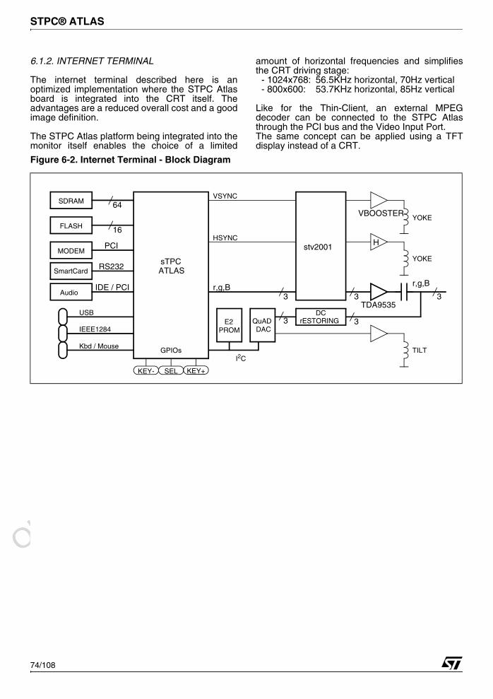
Obsolete Product(
s) - O
bsolete Product(
s)
Obsolete Product(
s) - O
bsolete Product(
s)
STPC® ATLAS
74/108
6.1.2. INTERNET TERMINAL
The internet terminal described here is anoptimized implementation where the STPC Atlasboard is integrated into the CRT itself. Theadvantages are a reduced overall cost and a goodimage definition.
The STPC Atlas platform being integrated into themonitor itself enables the choice of a limited
amount of horizontal frequencies and simplifiesthe CRT driving stage:
- 1024x768: 56.5KHz horizontal, 70Hz vertical- 800x600: 53.7KHz horizontal, 85Hz vertical
Like for the Thin-Client, an external MPEGdecoder can be connected to the STPC Atlasthrough the PCI bus and the Video Input Port.The same concept can be applied using a TFTdisplay instead of a CRT.
Figure 6-2. Internet Terminal - Block Diagram
H
r,g,B
TDA9535
3
3 3
VBOOSTERYOKE
YOKE
TILT
DCrESTORINGQuAD
DAC3
3
sTPC
E2PROM
stv2001
r,g,B
HSYNC
VSYNC
ATLAS
I2C
KEY- KEY+SEL
GPIOs
SDRAM 64
FLASH
MODEM
Audio
Kbd / Mouse
USB
IEEE1284
16
PCI
IDE / PCI
RS232SmartCard
1
Obsolete Product(
s) - O
bsolete Product(
s)
Obsolete Product(
s) - O
bsolete Product(
s)
STPC® ATLAS
75/108
6.2. STPC CONFIGURATION
The STPC is a very flexible product thanks todecoupled clock domains and to strap optionsenabling a user-optimized configuration.
As some trade off are often necessary, it isimportant to do an analysis of the applicationneeds prior to design a system based on thisproduct. The applicative constraints are usuallythe following:
- CPU performance- graphics / video performances- power consumption- PCI bandwidth- booting time- EMC
Some other elements can help to tune the choice:- Code size of CPU Consuming tasks - Data size and location
On the STPC side, the configurable parametersare the following:
- Synchronous / asynchronous mode- HCLK speed- MCLK speed- Local Bus / ISA bus
6.2.1. LOCAL BUS / ISA BUS
The selection between the ISA bus and the LocalBus is relatively simple. The first one is a standardbus but slow. The Local Bus is fast andprogrammable but doesn't support any DMA norexternal master mechanisms. The Table 6-1below summarize the selection:
Before implementing a function requiring DMAcapability on the ISA bus, it is recommended tocheck if it exists on PCI, or if it can be implementeddifferently, in order to use the local bus mode.
6.2.2. CLOCK CONFIGURATION
The CPU clock and the memory clock areindependent unless the "synchronous mode" strapoption is set (see the STRAP OPTIONS chapter).The potential clock configurations are then
The advantage of the synchronous modecompared to the asynchronous mode is a lowerlatency when accessing SDRAM from the CPU orthe PCI (saves 4 MCLK cycles for the first accessof the burst). For the same CPU to Memorytransfer performance, MCLK has to be roughlyhigher by 20MHz between SYNC and ASYNCmodes to get the same system performance level(example: 66MHz SYNC = 86MHz ASYNC) .In all cases, use SDRAM with CAS Latency equalsto 2 (CL2) for the best performances.
The advantage of the asynchronous mode is thecapability to reprogram the MCLK speed on the fly.This could help for applications where powerconsumption must be optimized.
The last, and more complex, information toconsider is the behaviour of the software. In casehigh CPU or FPU computation is needed, it issometime better to be in DX2-133/MCLK=66synchronous mode than DX2-133/MCLK=90asynchronous mode. This depends on the localityof the number crunching code and the amount ofdata manipulated.
The Table 6-3 below gives some examples. Theright column correspond to the configurationnumber as described in Table 6-2 :
Obviously, the values for HCLK or MCLK can bereduced compared to Table 6-2 in case there is noneed to push the device at its limits, or whenavoiding to use specific frequency ranges (FMradio band for example).
6.3. ARCHITECTURE RECOMMENDATIONS
This section describes the recommendimplementations for the STPC interfaces. Formore details, download the ReferenceSchematics from the STPC web site.
Table 6-1. Bus mode selection
Need SelectionLegacy I/O device (Floppy, ...), Super I/O ISA BusDMA capability (Soundblaster) ISA BusFlash, SRAM, basic I/O device Local BusFast boot Local BusBoot flash of 4MB or more Local BusProgrammable Chip Select Local Bus
Table 6-2. Main STPC modes
C ModeHCLKMHz
CPU clockclock ratio
MCLKMHz
1 Synchronous 66 133 (x2) 662 Asynchronous 66 133 (x2) 90
Table 6-3. Clock mode selection
Constraints CNeed CPU powerCritical code fits into L1 cache
1
Need CPU powerCode or data does not fit into L1 cache
3
Need flexible SDRAM speed 2
1
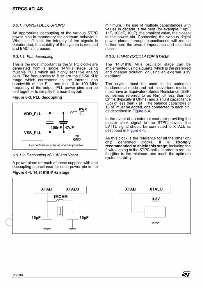
Obsolete Product(
s) - O
bsolete Product(
s)
Obsolete Product(
s) - O
bsolete Product(
s)
STPC® ATLAS
76/108
6.3.1. POWER DECOUPLING
An appropriate decoupling of the various STPCpower pins is mandatory for optimum behaviour.When insufficient, the integrity of the signals isdeteriorated, the stability of the system is reducedand EMC is increased.
6.3.1.1. PLL decoupling
This is the most important as the STPC clocks aregenerated from a single 14MHz stage usingmultiple PLLs which are highly sensitive analogcells. The frequencies to filter are the 25-50 KHzrange which correspond to the internal loopbandwidth of the PLL and the 10 to 100 MHzfrequency of the output. PLL power pins can betied together to simplify the board layout.
6.3.1.2. Decoupling of 3.3V and Vcore
A power plane for each of these supplies with onedecoupling capacitance for each power pin is the
minimum. The use of multiple capacitances withvalues in decade is the best (for example: 10pF,1nF, 100nF, 10uF), the smallest value, the closestto the power pin. Connecting the various digitalpower planes through capacitances will reducefurthermore the overall impedance and electricalnoise.
6.3.2. 14MHZ OSCILLATOR STAGE
The 14.31818 MHz oscillator stage can beimplemented using a quartz, which is the preferredand cheaper solution, or using an external 3.3Voscillator.
The crystal must be used in its series-cutfundamental mode and not in overtone mode. Itmust have an Equivalent Series Resistance (ESR,sometimes referred to as Rm) of less than 50Ohms (typically 8 Ohms) and a shunt capacitance(Co) of less than 7 pF. The balance capacitors of16 pF must be added, one connected to each pin,as described in Figure 6-4.
In the event of an external oscillator providing themaster clock signal to the STPC device, theLVTTL signal should be connected to XTALI, asdescribed in Figure 6-4.
As this clock is the reference for all the other on-chip generated clocks, it is stronglyrecommended to shield this stage, including the2 wires going to the STPC balls, in order to reducethe jitter to the minimum and reach the optimumsystem stability.
Figure 6-3. PLL decoupling
VDD_PLL
VSS_PLL
PWR
100nF 47uF
GND
Connections must be as short as possible
Figure 6-4. 14.31818 MHz stage
15pF15pF
XTALOXTALI XTALOXTALI
3.3V1MOHM
1

Obsolete Product(
s) - O
bsolete Product(
s)
Obsolete Product(
s) - O
bsolete Product(
s)
STPC® ATLAS
77/108
6.3.3. SDRAM
The STPC provides all the signals for SDRAMcontrol. Up to 128 MBytes of main memory aresupported. All Banks must be 64 bits wide. Up to 4memory banks are available when using 16Mbitdevices. Only up to 2 banks can be connectedwhen using 64Mbit and 128Mbit components dueto the reallocation of CS2# and CS3# signals. Thisis described in Table 6-4 and Table 6-5.
Graphics memory resides at the beginning of Bank0. Host memory begins at the top of graphics
memory and extends to the top of populatedSDRAM. Bank 0 must always be populated.
Figure 6-5, Figure 6-6 and Figure 6-7 show sometypical implementations.
The purpose of the serial resistors is to reducesignal oscillation and EMI by filtering linereflections. The capacitance in Figure 6-5 has afiltering effect too, while it is used for propagationdelay compensation in the 2 other figures.
For other implementations like 32-bit SDRAMdevices, refers to the SDRAM controller signal
multiplexing and address mapping described inthe following Table 6-4 and Table 6-5.
Figure 6-5. One Memory Bank with 4 Chips (16-bit)
Refer to Section 4.5.3. for detailed timing constraints.
CS0#
BA[1:0]MA[12:0]
WE#
RAS0#
DQM[7:0]
MCLKI
MCLKO
DQM[7:6]
Reference Knot
CAS0#
MD[63:48]DQM[5:4]MD[47:32]
DQM[3:2]MD[31:16]
DQM[1:0]MD[15:0]
MD[63:0]
MCLKAMCLKBMCLKCMCLKD
10pF
Length(MCLKI+1ns(+/- 0.5ns)) = Length(MCLKx) with x = A,B,C,D
1
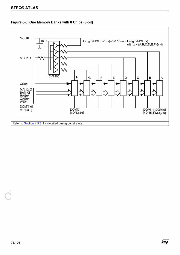
Obsolete Product(
s) - O
bsolete Product(
s)
Obsolete Product(
s) - O
bsolete Product(
s)
STPC® ATLAS
78/108
Figure 6-6. One Memory Banks with 8 Chips (8-bit)
Refer to Section 4.5.3. for detailed timing constraints.
CS0#
BA[1:0]MA[12:0]
WE#
RAS0#
DQM[7:0]
MCLKI
MCLKO
DQM[7]
CAS0#
MD[63:56]DQM[0]MD[7:0]
MD[63:0]
A
10pF Length(MCLKI+1ns(+/- 0.5ns)) = Length(MCLKx)
DQM[1]MD[15:8]
BCDEFGHCY2305
with x = A,B,C,D,E,F,G,H
1
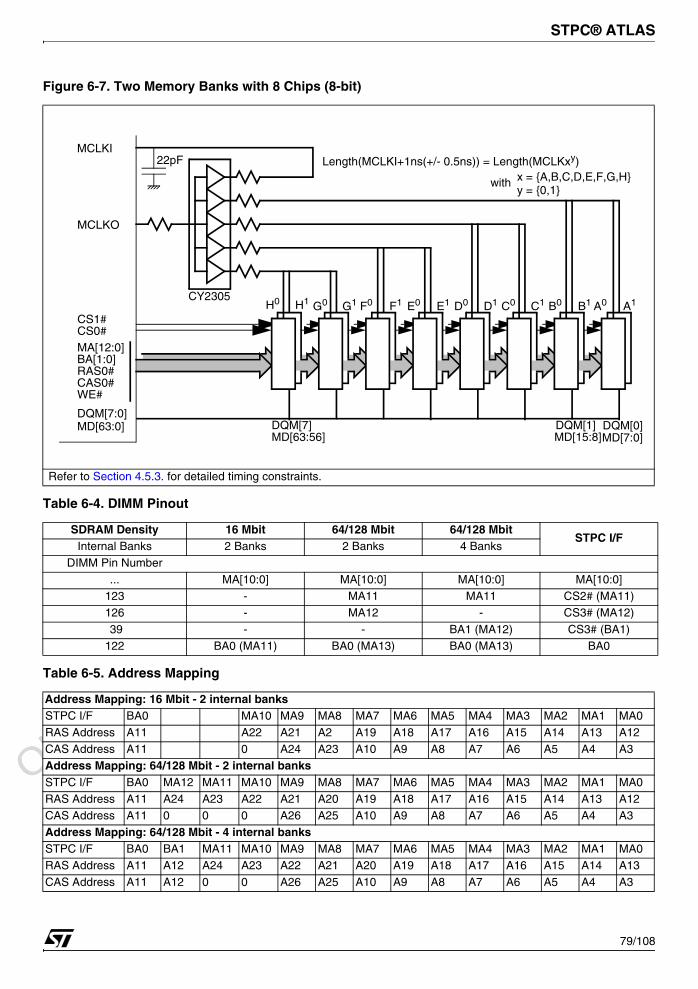
Obsolete Product(
s) - O
bsolete Product(
s)
Obsolete Product(
s) - O
bsolete Product(
s)
STPC® ATLAS
79/108
Figure 6-7. Two Memory Banks with 8 Chips (8-bit)
Refer to Section 4.5.3. for detailed timing constraints.
Table 6-4. DIMM Pinout
SDRAM Density 16 Mbit 64/128 Mbit 64/128 MbitSTPC I/F
Internal Banks 2 Banks 2 Banks 4 BanksDIMM Pin Number
... MA[10:0] MA[10:0] MA[10:0] MA[10:0]123 - MA11 MA11 CS2# (MA11)126 - MA12 - CS3# (MA12) 39 - - BA1 (MA12) CS3# (BA1)122 BA0 (MA11) BA0 (MA13) BA0 (MA13) BA0
Table 6-5. Address Mapping
Address Mapping: 16 Mbit - 2 internal banksSTPC I/F BA0 MA10 MA9 MA8 MA7 MA6 MA5 MA4 MA3 MA2 MA1 MA0 RAS Address A11 A22 A21 A2 A19 A18 A17 A16 A15 A14 A13 A12 CAS Address A11 0 A24 A23 A10 A9 A8 A7 A6 A5 A4 A3Address Mapping: 64/128 Mbit - 2 internal banksSTPC I/F BA0 MA12 MA11 MA10 MA9 MA8 MA7 MA6 MA5 MA4 MA3 MA2 MA1 MA0RAS Address A11 A24 A23 A22 A21 A20 A19 A18 A17 A16 A15 A14 A13 A12CAS Address A11 0 0 0 A26 A25 A10 A9 A8 A7 A6 A5 A4 A3Address Mapping: 64/128 Mbit - 4 internal banksSTPC I/F BA0 BA1 MA11 MA10 MA9 MA8 MA7 MA6 MA5 MA4 MA3 MA2 MA1 MA0RAS Address A11 A12 A24 A23 A22 A21 A20 A19 A18 A17 A16 A15 A14 A13CAS Address A11 A12 0 0 A26 A25 A10 A9 A8 A7 A6 A5 A4 A3
CS1#
BA[1:0]MA[12:0]
WE#
RAS0#
DQM[7:0]
MCLKI
MCLKO
DQM[7]
CAS0#
MD[63:56]DQM[0]MD[7:0]
MD[63:0]
A1
22pF Length(MCLKI+1ns(+/- 0.5ns)) = Length(MCLKxy)
DQM[1]MD[15:8]
B1C1D1E1F1G1H1
CS0#
A0B0C0D0E0F0G0H0CY2305
withy = 0,1x = A,B,C,D,E,F,G,H
1
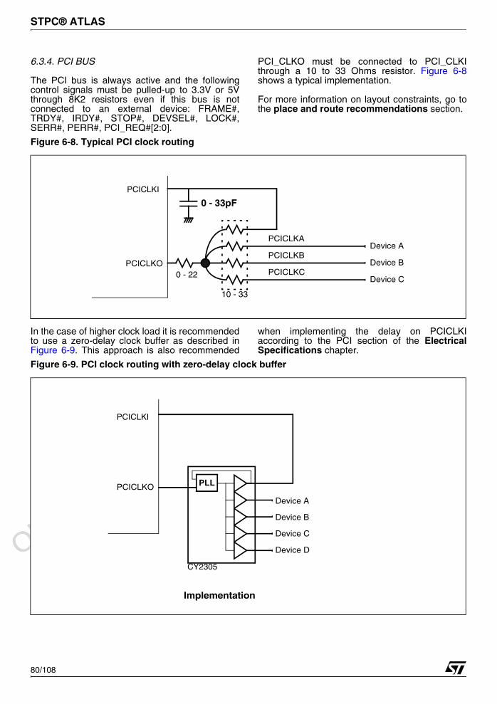
Obsolete Product(
s) - O
bsolete Product(
s)
Obsolete Product(
s) - O
bsolete Product(
s)
STPC® ATLAS
80/108
6.3.4. PCI BUS
The PCI bus is always active and the followingcontrol signals must be pulled-up to 3.3V or 5Vthrough 8K2 resistors even if this bus is notconnected to an external device: FRAME#,TRDY#, IRDY#, STOP#, DEVSEL#, LOCK#,SERR#, PERR#, PCI_REQ#[2:0].
PCI_CLKO must be connected to PCI_CLKIthrough a 10 to 33 Ohms resistor. Figure 6-8shows a typical implementation.
For more information on layout constraints, go tothe place and route recommendations section.
In the case of higher clock load it is recommendedto use a zero-delay clock buffer as described inFigure 6-9. This approach is also recommended
when implementing the delay on PCICLKIaccording to the PCI section of the ElectricalSpecifications chapter.
Figure 6-8. Typical PCI clock routing
PCICLKI
PCICLKO
PCICLKA
PCICLKB
PCICLKC0 - 22
10 - 33
Device A
Device B
Device C
0 - 33pF
Figure 6-9. PCI clock routing with zero-delay clock buffer
PCICLKI
PCICLKO
Device A
Device B
Device C
PLL
Device D
CY2305
Implementation
1
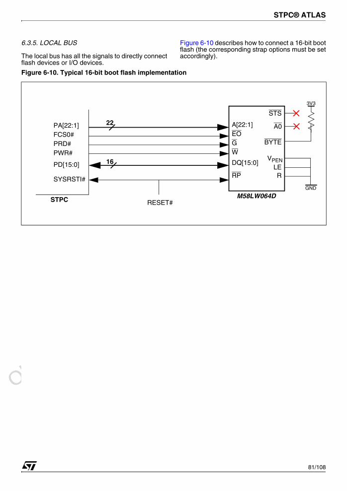
Obsolete Product(
s) - O
bsolete Product(
s)
Obsolete Product(
s) - O
bsolete Product(
s)
STPC® ATLAS
81/108
6.3.5. LOCAL BUS
The local bus has all the signals to directly connectflash devices or I/O devices.
Figure 6-10 describes how to connect a 16-bit bootflash (the corresponding strap options must be setaccordingly).
Figure 6-10. Typical 16-bit boot flash implementation
M58LW064DSTPC
22
DQ[15:0]
A[22:1]EOGW
RP
BYTE
VPEN
STS
LER
3V3
GND
RESET#
16PD[15:0]
FCS0#
PWR#
SYSRSTI#
PRD#
PA[22:1] A0
1

Obsolete Product(
s) - O
bsolete Product(
s)
Obsolete Product(
s) - O
bsolete Product(
s)
STPC® ATLAS
82/108
6.3.6. IPC
Most of the IPC signals are multiplexed: Interruptinputs, DMA Request inputs, DMA Acknowledgeoutputs. The figure below describes a completeimplementation of the IRQ[15:0] time-multiplexing.
When an interrupt line is used internally, thecorresponding input can be grounded. In most ofthe embedded designs, only few interrupts linesare necessary and the glue logic can be simplified.
When the interface is integrated into the STPC,the corresponding interrupt line can be groundedas it is connected internally.
For example, if the integrated IDE controller isactivated, the IRQ[14] and IRQ[15] inputs can begrounded.
Figure 6-11. Typical IRQ multiplexing
74x153
1C0
1Y
1G
IRQ[0]
IRQ_MUX[0]1C11C21C32C02C12C22C3AB
2G
2Y IRQ_MUX[1]
IRQ[1]IRQ[2]IRQ[3]IRQ[4]IRQ[5]IRQ[6]IRQ[7]
74x153
1C0
1Y
1G
IRQ_MUX[2]1C11C21C32C02C12C22C3AB
2G
2Y IRQ_MUX[3]
IRQ[8]IRQ[9]IRQ[10]IRQ[11]IRQ[12]IRQ[13]IRQ[14]IRQ[15]
ISA_CLK2XISA_CLK
Timer 0KeyboardSlave PICCOM2/COM4COM1/COM3LPT2
LPT1
RTC
MouseFPUPCI / IDEPCI / IDE
Floppy
Floppy
1

Obsolete Product(
s) - O
bsolete Product(
s)
Obsolete Product(
s) - O
bsolete Product(
s)
STPC® ATLAS
83/108
The figure below describes a completeimplementation of the external glue logic for DMARequest time-multiplexing and DMA Acknowledgedemultiplexing. Like for the interrupt lines, this
logic can be simplified when only few DMAchannels are used in the application.This glue logic is not needed in Local bus mode asit does not support DMA transfers.
Figure 6-12. Typical DMA multiplexing and demultiplexing
74x153
1C0
1Y
1G
DRQ[0]
DREQ_MUX[0]1C11C21C32C02C12C22C3AB
2G
2Y DREQ_MUX[1]
DRQ[1]DRQ[2]DRQ[3]DRQ[4]DRQ[5]DRQ[6]DRQ[7]
74x138
Y0#
A
G2B
DACK0#Y1#Y2#Y3#Y4#Y5#Y6#Y7#
CB
G2A
ISA_CLK2XISA_CLK
ISA, RefreshISA, PIOISA, FDCISA, PIOSlave DMACISAISAISA
G1
DMA_ENC[0]DMA_ENC[1]DMA_ENC[2]
DACK1#DACK2#DACK3#
DACK5#DACK6#DACK7#
1

Obsolete Product(
s) - O
bsolete Product(
s)
Obsolete Product(
s) - O
bsolete Product(
s)
STPC® ATLAS
84/108
6.3.7. IDE / ISA DYNAMIC DEMULTIPLEXING
Some of the ISA bus signals are dynamicallymultiplexed to optimize the pin count. Figure 6-13
describes how to implement the external glue logicto demultiplex the IDE and ISA interfaces. In LocalBus mode the two buffers are not needed and theNAND gates can be simplified to inverters.
6.3.8. BASIC AUDIO USING IDE INTERFACE
When the application requires only basic audiocapabilities, an audio DAC on the IDE interfacecan avoid using a PCI-based audio device(see
Figure 6-14). This low cost solution is not CPUconsuming thanks to the DMA controllerimplemented in the IDE controller and cangenerate 16-bit stereo sound. The clock speed isprogrammable when using the speaker output.
Figure 6-13. Typical IDE / ISA Demultiplexing
MASTER#74xx245
RMRTCCS#A B
DIR
OEISAOE#
KBCS#RTCRW#RTCDSSA[19:8]
STPC bus / DD[15:0]
LA[22]
LA[23]
LA[20]
LA[21]
SCS1#
SCS3#
PCS1#
PCS3#
Figure 6-14. Basic audio on IDE
74xx74
16
Q
Q
DD[15:0]
DPR
RST
D[15:0]CS#PCS1WR#A/B
Audio Out
Right
Left
Stereo DAC
PDRQSYSRSTO#
Speaker
PDIOW#
Vcc
Vcc
Vcc
STPC
Q
QDPR
RST
Note * : the inverter can be removed when the DAC CS# is directly connected to GND
*
1

Obsolete Product(
s) - O
bsolete Product(
s)
Obsolete Product(
s) - O
bsolete Product(
s)
STPC® ATLAS
85/108
6.3.9. VGA INTERFACE
The STPC integrates a voltage reference andvideo buffers. The amount of external devices isthen limited to the minimum as described in theFigure 6-15.
All the resistors and capacitors have to be as closeas possible to the STPC while the circuit protectorDALC112S1 must be close to the VGA connector.
The DDC[1:0] lines, not represented here, havealso to be protected when they are used on theVGA connector.
COL_SEL can be used when implementing thePicture-In-Picture function outside the STPC, forexample when multiplexing an analog videosource. In that case, the CRTC of the STPC has tobe genlocked to this analog source.
DCLK is usually used by the TFT display whichhas RGB inputs in order to synchronise the pictureat the level of the pixel.
When the VGA interface is not needed, the signalsR, G, B, HSYNC, VSYNC, COMP, RSET can beleft unconnected, VSS_DAC and VDD_DAC mustthen be connected to GND.
Figure 6-15. Typical VGA implementation
143
VDD_DACCOMP
VREF_DACRSET
VSS_DAC
2.5V10nF
100nF 47uF
AGND
COL_SELDCLK
HSYNCVSYNC
RGB
75 1%DALC112S1
AGND3.3V
100nF1%
1
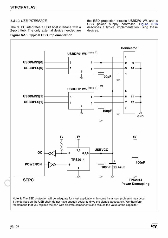
Obsolete Product(
s) - O
bsolete Product(
s)
Obsolete Product(
s) - O
bsolete Product(
s)
STPC® ATLAS
86/108
6.3.10. USB INTERFACE
The STPC integrates a USB host interface with a2-port Hub. The only external device needed are
the ESD protection circuits USBDF01W5 and aUSB power supply controller. Figure 6-16describes a typical implementation using thesedevices.
Figure 6-16. Typical USB implementation
POWERON
STPC
TPS2014
OC
USBDMNS[0]
USBDPLS[0]
USBDMNS[1]
USBDPLS[1]
5V
Connector
GND
9
10
11
12
1
2
6
7
3
4
8
5
100nF 2x 47uF
5
4
6,7,8
5V
2,3
1
USBVCC
100nF
5V
TPS2014Power Decoupling
R = 15 Ohm
R = 15 Ohm
R = 15 Ohm
R = 15 Ohm
USBDF01W5 (note 1)
1
3 4
52
R = 15 Ohm
R = 15 Ohm
USBDF01W5 (note 1)
1
3 4
52
Note 1: The ESD protection will be adequate for most applications. In some instances, problems may occur if the devices on the USB chain do not have enough power to drive the signals adequately. We thereforerecommend that you replace the part with discrete components and reduce the value of the capacitor.
100pF
100pF
1
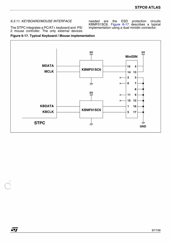
Obsolete Product(
s) - O
bsolete Product(
s)
Obsolete Product(
s) - O
bsolete Product(
s)
STPC® ATLAS
87/108
6.3.11. KEYBOARD/MOUSE INTERFACE
The STPC integrates a PC/AT+ keyboard and PS/2 mouse controller. The only external devices
needed are the ESD protection circuitsKBMF01SC6. Figure 6-17 describes a typicalimplementation using a dual minidin connector.
Figure 6-17. Typical Keyboard / Mouse implementation
MDATA
MCLK
KBDATA
KBCLK
STPC
5V
MiniDIN
GND
KBMF01SC6
4
13
3
7
8
9
12
16
17
5V
KBMF01SC6
5V
10
14
1
5
2
6
11
15
1

Obsolete Product(
s) - O
bsolete Product(
s)
Obsolete Product(
s) - O
bsolete Product(
s)
STPC® ATLAS
88/108
6.3.12. PARALLEL PORT INTERFACE
The STPC integrates a parallel port where the onlyexternal device needed is the ESD protection
circuits ST1284-01A8. Figure 6-18 describes atypical implementation using this device.
Figure 6-18. Typical parallel port implementation
ACK#
AUTOFD#
STROBE#
PD[7:0]
STPC
Connector
ST1284-01A8
5V
88
BUSY
PE
SLCT
SLCTIN#
INIT#
ERR#
1

Obsolete Product(
s) - O
bsolete Product(
s)
Obsolete Product(
s) - O
bsolete Product(
s)
STPC® ATLAS
89/108
6.3.13. JTAG INTERFACE
The STPC integrates a JTAG interface for scan-chain and on-board testing. The only external
device needed are the pull up resistors. Figure 6-19 describes a typical implementation using thesedevices.
6.4. PLACE AND ROUTE RECOMMENDATIONS
6.4.1. GENERAL RECOMMENDATIONS
Some STPC Interfaces run at high speed andneed to be carefully routed or even shielded like:
1) Memory Interface2) PCI bus3) Graphics and video interfaces4) 14 MHz oscillator stage
All clock signals have to be routed first andshielded for speeds of 27MHz or higher. The highspeed signals follow the same constraints, as forthe memory and PCI control signals.
The next interfaces to be routed are Memory, PCI,and Video/graphics.
All the analog noise-sensitive signals have to berouted in a separate area and hence can be routedindepedently.
6.4.2. PLL DEFINITION AND IMPLIMENTATION
PLLs are analog cells which supply the internalSTPC Clocks. To get the cleanest clock, the jitteron the power supply must be reduced as much aspossible. This will result in a more stable system.
Each of the integrated PLL has a dedicated powerpin so a single power plane for all of these PLLs, orone wire for each, or any solution in betweenwhich help the layout of the board can be used.
Powering these pins with one Ferrite +capacitances is enough. We recommend at least 2capacitances: one 'big' (few uF) for power storage,and one or 2 smalls (100nF + 1nF) for noisefiltering.
Figure 6-19. Typical JTAG implementation
STPC
TCLK
TDO
3V3 Connector
910
12
6
7
34
8
5
TMS
TDI
TRST
3V3 3V3 3V3
1

Obsolete Product(
s) - O
bsolete Product(
s)
Obsolete Product(
s) - O
bsolete Product(
s)
STPC® ATLAS
90/108
Figure 6-20. Shielding signals
ground ring
ground pad
shielded signal line
ground padshielded signal lines
1
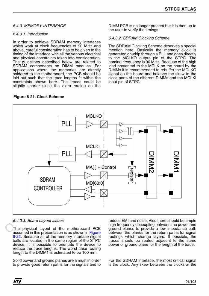
Obsolete Product(
s) - O
bsolete Product(
s)
Obsolete Product(
s) - O
bsolete Product(
s)
STPC® ATLAS
91/108
6.4.3. MEMORY INTERFACE
6.4.3.1. Introduction
In order to achieve SDRAM memory interfaceswhich work at clock frequencies of 90 MHz andabove, careful consideration has to be given to thetiming of the interface with all the various electricaland physical constraints taken into consideration.The guidelines described below are related toSDRAM components on DIMM modules. Forapplications where the memories are directlysoldered to the motherboard, the PCB should belaid out such that the trace lengths fit within theconstraints shown here. The traces could beslightly shorter since the extra routing on the
DIMM PCB is no longer present but it is then up tothe user to verify the timings.
6.4.3.2. SDRAM Clocking Scheme
The SDRAM Clocking Scheme deserves a specialmention here. Basically the memory clock isgenerated on-chip through a PLL and goes directlyto the MCLKO output pin of the STPC. Thenominal frequency is 90 MHz. Because of the highload presented to the MCLK on the board by theDIMMs it is recommended to rebuffer the MCLKOsignal on the board and balance the skew to theclock ports of the different DIMMs and the MCLKIinput pin of STPC.
6.4.3.3. Board Layout Issues
The physical layout of the motherboard PCBassumed in this presentation is as shown in Figure6-22. Because all of the memory interface signalballs are located in the same region of the STPCdevice, it is possible to orientate the device toreduce the trace lengths. The worst case routinglength to the DIMM1 is estimated to be 100 mm.
Solid power and ground planes are a must in orderto provide good return paths for the signals and to
reduce EMI and noise. Also there should be amplehigh frequency decoupling between the power andground planes to provide a low impedance pathbetween the planes for the return paths for signalroutings which change layers. If possible, thetraces should be routed adjacent to the samepower or ground plane for the length of the trace.
For the SDRAM interface, the most critical signalis the clock. Any skew between the clocks at the
Figure 6-21. Clock Scheme
DIM
M1
MCLKI
MCLKO
DIM
M2
PLL
register
PLL
MA[ ] + Control
MD[63:0]SDRAM
CONTROLLER

Obsolete Product(
s) - O
bsolete Product(
s)
Obsolete Product(
s) - O
bsolete Product(
s)
STPC® ATLAS
92/108
SDRAM components and the memory controllerwill impact the timing budget. In order to get wellmatched clocks at all components it isrecommended that all the DIMM clock pins, STPCmemory clock input (MCLKI) and any othercomponent using the memory clock areindividually driven from a low skew clock driverwith matched routing lengths specified in Section4.5.3. . In other words, all clock line lengths that go
from the buffer to the memory chips (MCLKx) andfrom the buffer to the STPC (MCLKI) must followthis equation;
MCLKx = MCLKI+(1ns+/-0.5ns).
This is shown in Figure 6-23.
Figure 6-22. DIMM placement
DIMM2
DIMM1
STPC
35mm
35mm
15mm
10mm
116mm
SDRAM I/F
Figure 6-23. Clock Routing
MCLKO
DIMM CKn input
STPC MCLKI
DIMM CKn input
DIMM CKn input
Low skew clock driver:L+(1ns+/- 0.5ns)
L+75mm*
20pF
* No additional 75mm when SDRAM directly soldered on board
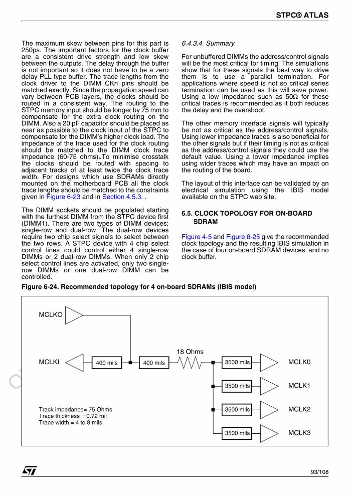
Obsolete Product(
s) - O
bsolete Product(
s)
Obsolete Product(
s) - O
bsolete Product(
s)
STPC® ATLAS
93/108
The maximum skew between pins for this part is250ps. The important factors for the clock bufferare a consistent drive strength and low skewbetween the outputs. The delay through the bufferis not important so it does not have to be a zerodelay PLL type buffer. The trace lengths from theclock driver to the DIMM CKn pins should bematched exactly. Since the propagation speed canvary between PCB layers, the clocks should berouted in a consistent way. The routing to theSTPC memory input should be longer by 75 mm tocompensate for the extra clock routing on theDIMM. Also a 20 pF capacitor should be placed asnear as possible to the clock input of the STPC tocompensate for the DIMM’s higher clock load. Theimpedance of the trace used for the clock routingshould be matched to the DIMM clock traceimpedance (60-75 ohms).To minimise crosstalkthe clocks should be routed with spacing toadjacent tracks of at least twice the clock tracewidth. For designs which use SDRAMs directlymounted on the motherboard PCB all the clocktrace lengths should be matched to the constraintsgiven in Figure 6-23 and in Section 4.5.3. .
The DIMM sockets should be populated startingwith the furthest DIMM from the STPC device first(DIMM1). There are two types of DIMM devices;single-row and dual-row. The dual-row devicesrequire two chip select signals to select betweenthe two rows. A STPC device with 4 chip selectcontrol lines could control either 4 single-rowDIMMs or 2 dual-row DIMMs. When only 2 chipselect control lines are activated, only two single-row DIMMs or one dual-row DIMM can becontrolled.
6.4.3.4. Summary
For unbuffered DIMMs the address/control signalswill be the most critical for timing. The simulationsshow that for these signals the best way to drivethem is to use a parallel termination. Forapplications where speed is not so critical seriestermination can be used as this will save power.Using a low impedance such as 50Ω for thesecritical traces is recommended as it both reducesthe delay and the overshoot.
The other memory interface signals will typicallybe not as critical as the address/control signals.Using lower impedance traces is also beneficial forthe other signals but if their timing is not as criticalas the address/control signals they could use thedefault value. Using a lower impedance impliesusing wider traces which may have an impact onthe routing of the board.
The layout of this interface can be validated by anelectrical simulation using the IBIS modelavailable on the STPC web site.
6.5. CLOCK TOPOLOGY FOR ON-BOARD SDRAM
Figure 4-5 and Figure 6-25 give the recommendedclock topology and the resulting IBIS simulation inthe case of four on-board SDRAM devices and noclock buffer.
Figure 6-24. Recommended topology for 4 on-board SDRAMs (IBIS model)
MCLKI
MCLKO
18 Ohms
400 mils 3500 mils
3500 mils
3500 mils
3500 mils
400 mils MCLK0
MCLK1
MCLK2
MCLK3
Track impedance= 75 OhmsTrace thickness = 0.72 milTrace width = 4 to 8 mils
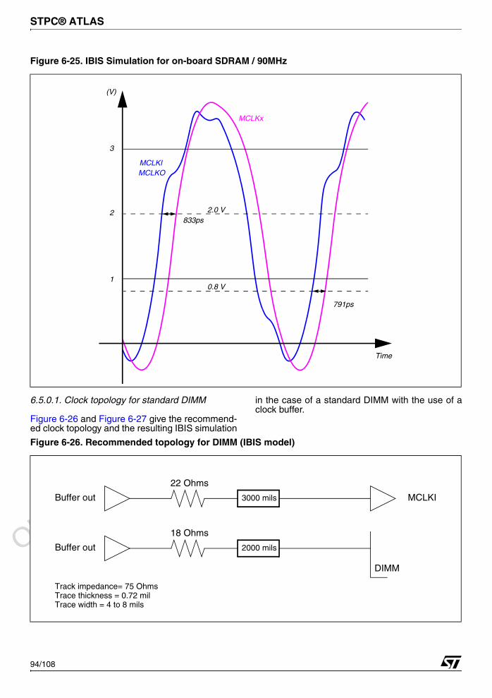
Obsolete Product(
s) - O
bsolete Product(
s)
Obsolete Product(
s) - O
bsolete Product(
s)
STPC® ATLAS
94/108
6.5.0.1. Clock topology for standard DIMM
Figure 6-26 and Figure 6-27 give the recommend-ed clock topology and the resulting IBIS simulation
in the case of a standard DIMM with the use of aclock buffer.
Figure 6-25. IBIS Simulation for on-board SDRAM / 90MHz
0.8 V
2.0 V833ps
791ps
3
2
1
MCLKIMCLKO
(V)
MCLKx
Time
Figure 6-26. Recommended topology for DIMM (IBIS model)
MCLKI
22 Ohms
3000 mils
Track impedance= 75 OhmsTrace thickness = 0.72 milTrace width = 4 to 8 mils
Buffer out
18 Ohms
2000 mils
DIMM
Buffer out
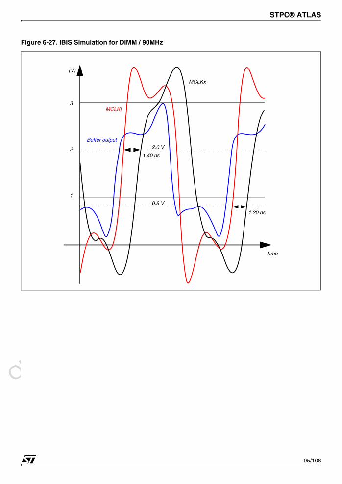
Obsolete Product(
s) - O
bsolete Product(
s)
Obsolete Product(
s) - O
bsolete Product(
s)
STPC® ATLAS
95/108
Figure 6-27. IBIS Simulation for DIMM / 90MHz
3
2
1
(V)
Time
0.8 V
2.0 VBuffer output
MCLKI
MCLKx
1.40 ns
1.20 ns

Obsolete Product(
s) - O
bsolete Product(
s)
Obsolete Product(
s) - O
bsolete Product(
s)
STPC® ATLAS
96/108
6.5.1. PCI INTERFACE
6.5.1.1. Introduction
In order to achieve a PCI interface which work atclock frequencies up to 33MHz, carefulconsideration has to be given to the timing of theinterface with all the various electrical and physicalconstraints taken into consideration.
6.5.1.2. PCI Clocking Scheme
The PCI Clocking Scheme deserves a specialmention here. Basically the PCI clock (PCICLKO)is generated on-chip from HCLK through aprogrammable delay line and a clock divider. Thenominal frequency is 33MHz. This clock must belooped to PCICLKI and goes to the internal SouthBridge through a deskewer. On the contrary, theinternal North Bridge is clocked by HCLK, puttingsome additionnal constraints on T0 and T1.
6.5.1.3. Board Layout Issues
The physical layout of the motherboard PCBassumed in this presentation is as shown in Figure6-29. For the PCI interface, the most critical signalis the clock. Any skew between the clocks at thePCI components and the STPC will impact thetiming budget. In order to get well matched clocksat all components it is recommended that all thePCI clocks are individually driven from a serialresistance with matched routing lengths. In otherwords, all clock line lengths that go from theresistor to the PCI chips (PCICLKx) must beidentical.
The figure below is for PCI devices soldered on-board. In the case of a PCI slot, the wire lengthmust be shortened by 2.5" to compensate theclock layout on the PCI board. The maximum clockskew between all devices is 2ns according to PCIspecifications.
The Figure 6-30 describes a typical clock delayimplementation. The exact timing constraints arelisted in the PCI section of the ElectricalSpecifications Chapter.
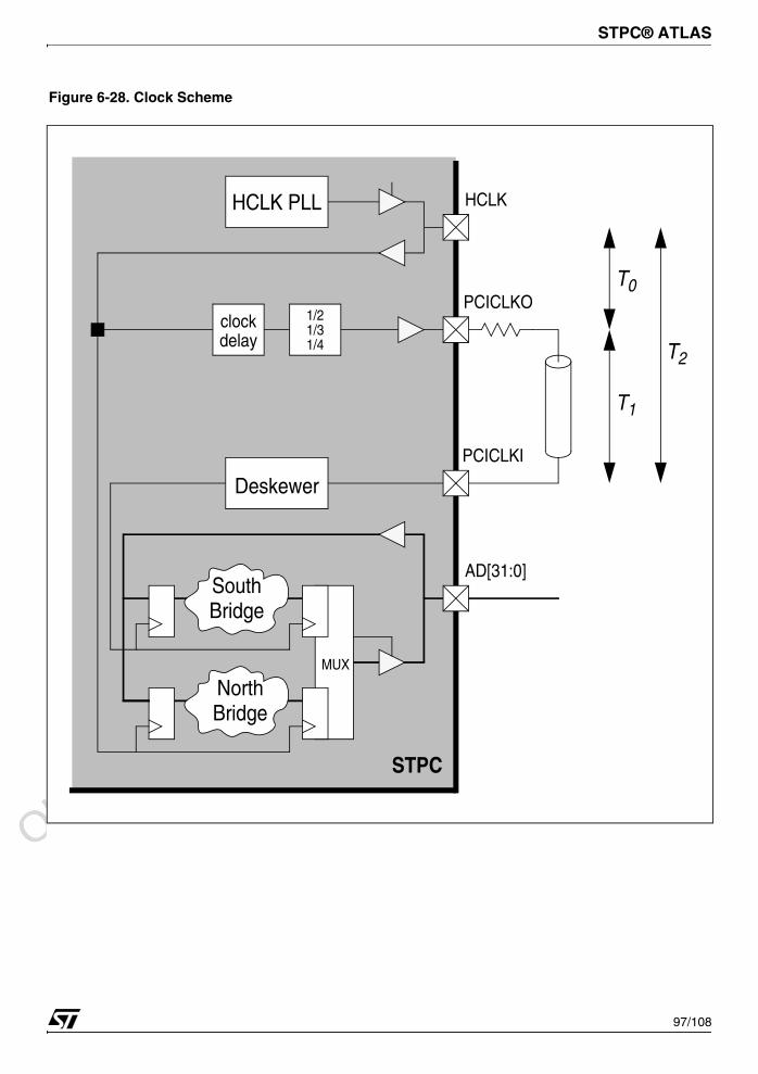
Obsolete Product(
s) - O
bsolete Product(
s)
Obsolete Product(
s) - O
bsolete Product(
s)
STPC® ATLAS
97/108
Figure 6-28. Clock Scheme
HCLK PLL
1/21/31/4
clockPCICLKO
T1
PCICLKI
HCLK
AD[31:0]South
North
Deskewer
MUX
T0
T2delay
STPC
Bridge
Bridge

Obsolete Product(
s) - O
bsolete Product(
s)
Obsolete Product(
s) - O
bsolete Product(
s)
STPC® ATLAS
98/108
Figure 6-29. Typical PCI clock routing
Figure 6-30. Clocks relationships
Length(PCICLKI) = Length(PCICLKx) with x = A,B,C
Note: The value of 22 Ohms corresponds to tracks with Z0 = 70 Ohms.
PCICLKI
PCICLKO
PCICLKA
PCICLKB
PCICLKC
Device A
Device B
Device C
PCICLKO
PCICLKI
HCLK
PCICLKx
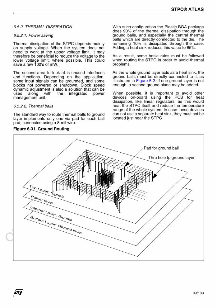
Obsolete Product(
s) - O
bsolete Product(
s)
Obsolete Product(
s) - O
bsolete Product(
s)
STPC® ATLAS
99/108
6.5.2. THERMAL DISSIPATION
6.5.2.1. Power saving
Thermal dissipation of the STPC depends mainlyon supply voltage. When the system does notneed to work at the upper voltage limit, it maytherefore be beneficial to reduce the voltage to thelower voltage limit, where possible. This couldsave a few 100’s of mW.
The second area to look at is unused interfacesand functions. Depending on the application,some input signals can be grounded, and someblocks not powered or shutdown. Clock speeddynamic adjustment is also a solution that can beused along with the integrated powermanagement unit.
6.5.2.2. Thermal balls
The standard way to route thermal balls to groundlayer implements only one via pad for each ballpad, connected using a 8-mil wire.
With such configuration the Plastic BGA packagedoes 90% of the thermal dissipation through theground balls, and especially the central thermalballs which are directly connected to the die. Theremaining 10% is dissipated through the case.Adding a heat sink reduces this value to 85%.
As a result, some basic rules must be followedwhen routing the STPC in order to avoid thermalproblems.
As the whole ground layer acts as a heat sink, theground balls must be directly connected to it, asillustrated in Figure 5-2. If one ground layer is notenough, a second ground plane may be added.
When possible, it is important to avoid otherdevices on-board using the PCB for heatdissipation, like linear regulators, as this wouldheat the STPC itself and reduce the temperaturerange of the whole system, In case these devicescan not use a separate heat sink, they must not belocated just near the STPC
Figure 6-31. Ground Routing
Thru hole to ground layer
Top Layer: SignalsPower layerInternal Layer: SignalsBottom Layer: Ground layer
Pad for ground ball

Obsolete Product(
s) - O
bsolete Product(
s)
Obsolete Product(
s) - O
bsolete Product(
s)
STPC® ATLAS
100/108
When considering thermal dissipation, one of themost important parts of the layout is theconnection between the ground balls and theground layer.
A 1-wire connection is shown in Figure 5-1. Theuse of a 8-mil wire results in a thermal resistanceof 105°C/W assuming copper is used (418 W/m.°K). This high value is due to the thickness (34µm) of the copper on the external side of the PCB.
Considering only the central matrix of 36 thermalballs and one via for each ball, the global thermalresistance is 2.9°C/W. This can be easilyimproved using four 12.5 mil wires to connect to
the four vias around the ground pad link as inFigure 6-33. This gives a total of 49 vias and aglobal resistance for the 36 thermal balls of 0.5°C/W.
The use of a ground plane like in Figure 6-34 iseven better.
Figure 6-32. Recommended 1-wire Power/Ground Pad Layout
Solder Mask (4 mil)
Pad for ground ball (diameter = 25 mil)
Hole to ground layer (diameter = 12 mil)
Connection Wire (width = 12.5 mil)
Via (diameter = 24 mil)34.5 mil
1 mil = 0.0254 mm
Figure 6-33. Recommended 4-wire Ground Pad Layout
4 via pads for each ground ball
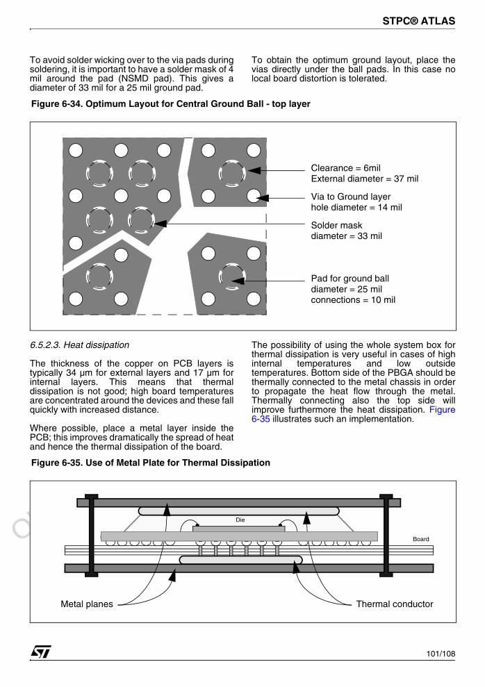
Obsolete Product(
s) - O
bsolete Product(
s)
Obsolete Product(
s) - O
bsolete Product(
s)
STPC® ATLAS
101/108
To avoid solder wicking over to the via pads duringsoldering, it is important to have a solder mask of 4mil around the pad (NSMD pad). This gives adiameter of 33 mil for a 25 mil ground pad.
To obtain the optimum ground layout, place thevias directly under the ball pads. In this case nolocal board distortion is tolerated.
6.5.2.3. Heat dissipation
The thickness of the copper on PCB layers istypically 34 µm for external layers and 17 µm forinternal layers. This means that thermaldissipation is not good; high board temperaturesare concentrated around the devices and these fallquickly with increased distance.
Where possible, place a metal layer inside thePCB; this improves dramatically the spread of heatand hence the thermal dissipation of the board.
The possibility of using the whole system box forthermal dissipation is very useful in cases of highinternal temperatures and low outsidetemperatures. Bottom side of the PBGA should bethermally connected to the metal chassis in orderto propagate the heat flow through the metal.Thermally connecting also the top side willimprove furthermore the heat dissipation. Figure6-35 illustrates such an implementation.
Figure 6-34. Optimum Layout for Central Ground Ball - top layer
Via to Ground layer
Pad for ground ball
Clearance = 6mil
diameter = 25 mil
hole diameter = 14 mil
Solder maskdiameter = 33 mil
External diameter = 37 mil
connections = 10 mil
Figure 6-35. Use of Metal Plate for Thermal Dissipation
Metal planes Thermal conductor
Board
Die
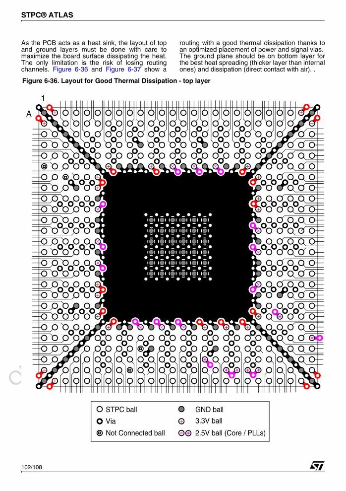
Obsolete Product(
s) - O
bsolete Product(
s)
Obsolete Product(
s) - O
bsolete Product(
s)
STPC® ATLAS
102/108
As the PCB acts as a heat sink, the layout of topand ground layers must be done with care tomaximize the board surface dissipating the heat.The only limitation is the risk of losing routingchannels. Figure 6-36 and Figure 6-37 show a
routing with a good thermal dissipation thanks toan optimized placement of power and signal vias.The ground plane should be on bottom layer forthe best heat spreading (thicker layer than internalones) and dissipation (direct contact with air). .
Figure 6-36. Layout for Good Thermal Dissipation - top layer
1
A
3.3V ball
2.5V ball (Core / PLLs)
Via
STPC ball GND ball
Not Connected ball

Obsolete Product(
s) - O
bsolete Product(
s)
Obsolete Product(
s) - O
bsolete Product(
s)
STPC® ATLAS
103/108
Figure 6-37. Recommend signal wiring (top & ground layers) with corresponding heat flow
Power/GND balls
Signal balls
External row
Internal row
GND PowerPower GND
Power/GND balls
Signal balls
Keep-Out = 6 mils
Obsolete Product(
s) - O
bsolete Product(
s)
Obsolete Product(
s) - O
bsolete Product(
s)
STPC® ATLAS
104/108
6.6. DEBUG METHODOLOGY
In order to bring a STPC-based board to life withthe best efficiency, it is recommended to follow thecheck-list described in this section.
6.6.1. POWER SUPPLIES
In parallel with the assembly process, it is useful toget a bare PCB to check the potential short-circuitsbetween the various power and ground planes.This test is also recommended when the firstboards are back from assembly. This will avoidbad surprises in case of a short-circuit due to abad soldering.
When the system is powered, all power supplies,including the PLL power pins must be checked tobe sure the right level is present. See Table 4-2 forthe exact supported voltage range:
VDD_CORE: 2.5VVDD_xxxPLL: 2.5VVDD: 3.3V
6.6.2. BOOT SEQUENCE
6.6.2.1. Reset input
The checking of the reset sequence is the nextstep. The waveform of SYSRSTI# must complieswith the timings described in Figure 4-3. Thissignal must not have glitches and must stay lowuntil the 14.31818MHz output (OSC14M) is at theright frequency and the strap options are stabilizedto a valid configuration.
In case this clock is not present, check the 14MHzoscillator stage (see Figure 6-4).
6.6.2.2. Strap options
The STPC has been designed in a way to allowconfigurations for test purpose that differs from thefunctional configuration. In many cases, thetroubleshootings at this stage of the debug are theresulting of bad strap options. This is why it ismandatory to check they are properly setup andsampled during the boot sequence.
The list of all the strap options is summarized atthe beginning of Section 3.
6.6.2.3. Clocks
Once OSC14M is checked and correct, the nextsignals to measure are the Host clock (HCLK), PCIclocks (PCI_CLKO, PCI_CLKI) and Memory clock(MCLKO, MCLKI).
HCLK must run at the speed defined by thecorresponding strap options (see Table 3-1). In x2CPU clock mode, this clock must be limited to66MHz.
PCI_CLKI and PCI_CLKO must be connected asdescribed in Figure 6-29 and not be higher than33MHz. Their speed depends on HCLK and on thedivider ratio defined by the MD[4] and MD[17] strapoptions as described in Section 3.To ensure a correct behaviour of the device, thePCI deskewing logic must be configured properlyby the MD[7:6] strap options according to Section3. For timings constraints, refers to Section 4.
1) MCLKI and MCLKO must be connected asdescribed in Figure 6-5 to Figure 6-7 depending onthe SDRAM implementation. The memory clockmust run at HCLK speed when in synchronousmode and must not be higher than 90MHz in anycase. The MCLK interface will run 100MHzoperation is possible but board layout is so criticalthat 90MHz maximum operation is recommended.
6.6.2.4. Reset output
If SYSRSTI# and all clocks are correct, then theSYSRSTO# output signal should behave asdescribed in Figure 4-3.
6.6.3. ISA MODE
Prior to check the ISA bus control signals,PCI_CLKI, ISA_CLK, ISA_CLK2X, and DEV_CLKmust be running properly. If it is not the case, it isprobably because one of the previous steps hasnot been completed.
6.6.3.1. First code fetches
When booting on the ISA bus, the two key signalsto check at the very beginning are RMRTCCS#and FRAME#.
The first one is a Chip Select for the boot flash andis multiplexed with the IDE interface. It shouldtoggle together with ISAOE# and MEMRD# tofetch the first 16 bytes of code. This correspondsto the loading of the first line of the CPU cache.
In case RMRTCCS# does not toggle, it is thennecessary to check the PCI FRAME# signal.Indeed the ISA controller is part of the SouthBridge and all ISA bus cycles are visible on thePCI bus.
If there is no activity on the PCI bus, then one ofthe previous steps has not been checked properly.If there is activity then there must be somethingconflicting on the ISA bus or on the PCI bus.
6.6.3.2. Boot Flash size
The ISA bus supports 8-bit and 16-bit memorydevices. In case of a 16-bit boot flash, the signalMEMCS16# must be activated duringRMRTCCS# cycle to inform the ISA controller of a16-bit device.
Obsolete Product(
s) - O
bsolete Product(
s)
Obsolete Product(
s) - O
bsolete Product(
s)
STPC® ATLAS
105/108
6.6.3.3. POST code
Once the 16 first bytes are fetched and decoded,the CPU core continue its execution depending onthe content of these first data. Usually, itcorresponds to a JUMP instruction and the codefetching continues, generating read cycles on theISA bus.
Most of the BIOS and boot loaders are reading thecontent of the flash, decompressing it in SDRAM,and then continue the execution by jumping to theentry point in RAM. This boot process ends with aJUMP to the entry point of the OS launcher.These various steps of the booting sequence arecodified by the so-called POST codes (Power-OnSelf-Test). A 8-bit code is written to the port 80H atthe beginning of each stage of the booting process(I/O write to address 0080H) and can be displayedon two 7-segment display, enabling a fast visualcheck of the booting completion level.Usually, the last POST code is 0x00 andcorresponds to the jump into the OS launcher.
When the execution fails or hangs, the lastestwritten code stays visible on that display,indicating either the piece of code to analyse,either the area of the hardware not workingproperly.
6.6.4. LOCAL BUS MODE
As the Local Bus controller is located into the Hostinterface, there is no access to the cycles on thePCI, reducing the amount of signals to check.
6.6.4.1. First code fetches
When booting on the Local Bus, the key signal tocheck at the very beginning is FCS0#. This signalis a Chip Select for the boot flash and shouldtoggle together with PRD# to fetch the first 16bytes of code. This corresponds to the loading ofthe first line of the CPU cache.In case FCS0# does not toggle, then one of the
previous steps has not been done properly, likeHCLK speed and CPU clock multiplier (x1, x2).
6.6.4.2. Boot Flash size
The Local Bus support 8-bit and 16-bit bootmemory devices only.
6.6.4.3. POST code
Like in ISA mode, POST codes can beimplemented on the Local Bus. The difference isthat an IOCS# must be programmed at I/Oaddress 80H prior to writing these code, the POSTdisplay being connected to this IOCS# and to thelower 8 bits of the bus.
6.6.5. SUMMARY
Here is a check-list for the STPC board debugfrom power-on to CPU execution.
For each step, in case of failure, verify first thecorresponding balls of the STPC:- check if the voltage or activity is correct- search for potential shortcuts.For troubleshooting in steps 5 to 10, verify the related strap options:- value & connection. Refer to Section 3.- see Figure 4-3 for timing constraintsSteps 8a and 9a are for debug in ISA mode while steps 8b and 9b are for Local Bus mode.
6.6.6. PCMCIA modeAs the STPC uses the RMRTCCS# signal for booting in that mode, the methodology is the same as for the ISA bus. The PCMCIA cards being 3.3V or 5V, the boot flash device must be 5V tolerant when directly connected on the address and data busses. An other solution is to isolate the flash from the PCMCIA lines using 5V tolerant LVTTL buffers.
Check: How? Troubleshooting
1Power
supplies
Verify that voltage is within specs:- this must include HF & LF noise- avoid full range sweepRefer to Table 4-1 for values
Measure voltage near STPC balls:- use very low GND connection.Add some decoupling capacitor:- the smallest, the nearest to STPC balls.
2 14.318 MHz Verify OSC14M speedThe 2 capacitors used with the quartz must match with the capacitance of the crystal.Try other values.
3SYSRSTI#
(Power Good)Measure SYSRSTI# of STPCSee Figure 4-3 for waveforms.
Verify reset generation circuit:- device reference- components value
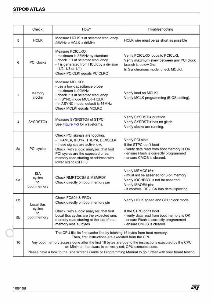
Obsolete Product(
s) - O
bsolete Product(
s)
Obsolete Product(
s) - O
bsolete Product(
s)
STPC® ATLAS
106/108
5 HCLKMeasure HCLK is at selected frequency25MHz < HCLK < 66MHz
HCLK wire must be as short as possible
6 PCI clocks
Measure PCICLKO:- maximum is 33MHz by standard- check it is at selected frequency- it is generated from HCLK by a division (1/2, 1/3 or 1/4)Check PCICLKI equals PCICLKO
Verify PCICLKO loops to PCICLKI.Verify maximum skew between any PCI clock branch is below 2ns.In Synchronous mode, check MCLKI.
7Memory clocks
Measure MCLKO:- use a low-capacitance probe- maximum is 90MHz- check it is at selected frequency- In SYNC mode MCLK=HCLK- in ASYNC mode, default is 66MHzCheck MCLKI equals MCLKO
Verify load on MCLKI.Verify MCLK programming (BIOS setting).
4 SYSRSTO#Measure SYSRSTO# of STPCSee Figure 4-3 for waveforms.
Verify SYSRSTI# duration.Verify SYSRSTI# has no glitchVerify clocks are running.
8a PCI cycles
Check PCI signals are toggling:- FRAME#, IRDY#, TRDY#, DEVSEL#- these signals are active low.Check, with a logic analyzer, that first PCI cycles are the expected ones: memory read starting at address with lower bits to 0xFFF0
Verify PCI slotsIf the STPC don’t boot- verify data read from boot memory is OK- ensure Flash is correctly programmed- ensure CMOS is cleared.
9a
ISAcycles
toboot memory
Check RMRTCCS# & MEMRD#Check directly on boot memory pin
Verify MEMCS16#:- must not be asserted for 8-bit memoryVerify IOCHRDY is not be assertedVerify ISAOE# pin:- it controls IDE / ISA bus demultiplexing
8bLocal Bus
cyclesto
boot memory
Check FCS0# & PRD#Check directly on boot memory pin
Verify HCLK speed and CPU clock mode.
9b
Check, with a logic analyzer, that first Local Bus cycles are the expected one: memory read starting at the top of boot memory less 16 bytes
If the STPC don’t boot- verify data read from boot memory is OK- ensure Flash is correctly programmed- ensure CMOS is cleared.
10
The CPU fills its first cache line by fetching 16 bytes from boot memory.Then, first instructions are executed from the CPU.
Any boot memory access done after the first 16 bytes are due to the instructions executed by the CPU=> Minimum hardware is correctly set, CPU executes code.
Please have a look to the Bios Writer’s Guide or Programming Manual to go further with your board testing.
Check: How? Troubleshooting

Obsolete Product(
s) - O
bsolete Product(
s)
Obsolete Product(
s) - O
bsolete Product(
s)
STPC® ATLAS
107/108
7 ORDERING DATA
7.1. ORDERING CODES
7.2 AVAILABLE PART NUMBERS
ST PC I2 H E Y C
STMicroelectronics
Prefix
Product Family
PC: PC Compatible
Product ID
I2: Atlas
Core Speed
G: 120 MHz
H: 133 MHz
Memory Speed
D: 90 MHz
E: 100 MHz
Package
Y: 516 Overmoulded BGA
Temperature Range
C: CommercialTcase = 0 to +85°C
I: IndustrialTcase = -40 to +115°C
Part NumberCore Frequency
(MHz)CPU Mode
Memory Interface Speed (MHz)
Tcase Range(C)
Operating Voltage(V)
STPCI2HEYC1 133 X2 90 0°C to +85°C 2.45 - 2.7
3.0 - 3.6STPCI2GDYI 120 X2 90 -40°C to +115°C
Note 1:The STPC Atlas MClock signal can run up to 100MHz reliably, but PCB layout is so critical that the maximum guaranteed speed is 90MHz
Obsolete Product(
s) - O
bsolete Product(
s)
Obsolete Product(
s) - O
bsolete Product(
s)
STPC® ATLAS
108/108
8 REVISION HISTORY
Date Revision Description of Changes
Mar 04 1.1 Second release
Jan 05 3
Revision number incremented from 1.1 to 3 due to Internal Document Management System changeModified Figure 6-9.PCI clock routing with zero-delay clock bufferAdded two capacitors (100pF) in Figure 6-16.Typical USB implementation.
Information furnished is believed to be accurate and reliable. However, STMicroelectronics assumes no responsibility for the consequencesof use of such information nor for any infringement of patents or other rights of third parties which may result from its use. No license is grantedby implication or otherwise under any patent or patent rights of STMicroelectronics. Specifications mentioned in this publication are subjectto change without notice. This publication supersedes and replaces all information previously supplied. STMicroelectronics products are notauthorized for use as critical components in life support devices or systems without express written approval of STMicroelectronics.
The ST logo is a registered trademark of STMicroelectronics.
All other names are the property of their respective owners
© 2005 STMicroelectronics - All rights reserved
STMicroelectronics group of companies
Australia – Belgium - Brazil - Canada - China – Czech Republic - Finland - France - Germany - Hong Kong - India - Israel - Italy - Japan - Malaysia - Malta - Morocco - Singapore - Spain - Sweden - Switzerland - United Kingdom - United States of America
www.st.com