Embed Size (px)
Citation preview
ANALOGDEVICES fAX-ON-DEMAND HOTLINE - Page 2
~ ANALOGW DEVICES
FEATURESAn 80MHz Bandwidth Permitting a 50Mb/s Data
Transfer RateA Variable Gain Amplifier with JOdB max Gain
and 40dB Control RangeTwo Gain of 4 RF Buffers200n Differential load Drive CapabilityA Pair of Precision RectifiersAGC level and Threshold OutputsAn Averaging, High Gain Sample-and-Hold for
Accurate AGC OperationTypical Gain Drift in Hold Mode: 0.2dB/msGains Trimmed and Temperature CompensatedAGC Operation Independent of AGC levelSymmetrical AGC Attack/Decay Times1J.ls AGC Attack/Decay Times Using a 1000pF
External CapacitorSuitable for Use as an Accurate Video Programmable
Gain AmplifierDynamic Clamp Ensures Fast Recovery After Write to
Read TransientsAGC RF Output level is Internally Preset
PRODUCT DESCRIPTIONThe AD890 is primarily intended for high-performance disksubsystem use and as such it is configured around the classicread channel processing block diagram. It is intended to beconnected between the head preamplifier and the qualificationcircuitry required for digital data recovery. When used with theA0891 rigid disk data qualifier, data transfer rates in excess ofSOMb/s can be processed.
A temperature-compensated AGC loop, with an exponentialtransfer characteristic, permits optimal settling and allows forpredictable performance in the classic single integrator controlloop configuration. Fast acquisition and low droop while in thehold mode allow for AGC operation to be performed within thesector header without compromising channel behavior whenreading data.
The AD890 processing clement has the flexibility to performboth continuous and sampled AGC functions; it is also ideal forembedded, dedicated, or mixed servo applications. Two user-defined filter/equalizer stages may be employed, thus allowingmaximum design flexibility. This greatly simplifies the design ofthe overall channel characteristics. Using the AD890, the designerno longer needs to resort 10passive techniques to isolate networkfunctions; this avoids problems of signal loss and interaction.Two low-offset, IOOMHzfull-wave rectifiers provide the capabilityto track a 1V peak signal. The rectifier generating the "Qualifier
Information furnished by Analog Devicl!$ is believed to be accurateand reliable. However, no responsibility is assumed by Analog Devicesfor its use; nor for any infringements of patents or other rights of thirdparties which may result from its use. No license is granted by implica'tion or otherwise under any patent or patent rights of Analog Devices.
---
Precision,WidebandChannelProcessingElement
.0'40.i., ,~.. .. . ~9oi"""'i;1,, '.
'.\Jil
.
'
..
'
.
'
.
'
.
iI.
"'
,..
'
. ,. . . etrrnrlt
o~~"11\.0890
, ""n~O~!t~,..0&90
""",'
Threshold" output may be used lor creating a dara qualificationlevel. A second rectifier is used to drive the sample-and-holdcircuitry.
The 80MHz bandwidth of the A0890 ensures good phase linearityup to SOMHz. Thus, data transfer rates in excess of SOMbfscanbe supported with good error rates and predictable channelbehavior.
The AD890 is available in both a 24-pill, slim-line cerdip packageand in a 28-pin PLCC package and is specified to operarc overthe 0 to 70DCcommercial temperatUre range.
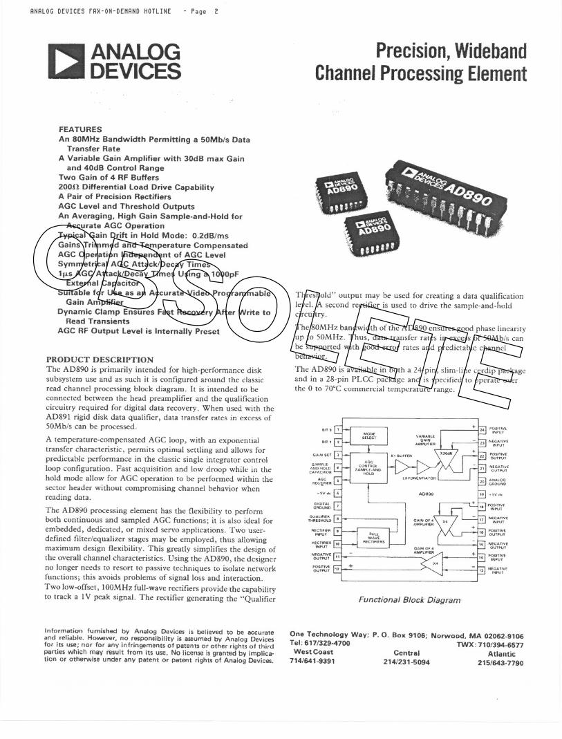
NEGATIVE,",uT
GAIN SET 1 J
SAMPt''NO,HOLD ,.
CAP4C"OH
HEttj~"HI ,
211~~~;~~'
201 ~~~t%~
g~rg~~'o I ,r~~~~~:~~D 1 . "I N~:::J\yE
"'CTJ'~H I .'NPU'"'CT""RI..',,"UT ..1 NEGAtlv,
OUTPUT
NJ~~;~~E I "
~b';~i:i 117 111 N~~:,j\VE
Functional Block Diagram
One Tec:hnology Way; P. O. Box 9106; Norwood, MA 02062-9106Tel: 617/329-4700 TWX: 710/394-6577West Coast Central Atlantic
714/641-9391 214/231-5094 215/643-7790
OBSOLETE
ANALOGDEVICES fAX-ON-DEHAND HOTLINE - Page 3
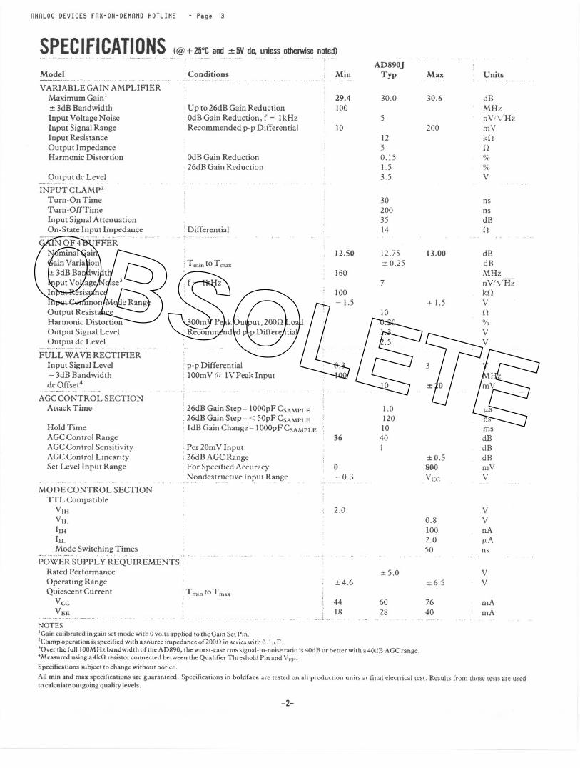
SPECIFICATIONS(@)+25OC and :!=5Vdc. unlessotherwisenoted)
Model
VARIABLE GAIN AMPLIFIERMaximum Gain I:t 3dBBandwidth
Input Voltage NoiseInput Signal RangeInput ResistanceOutput ImpedanceHarmonic Distortion
Output dc Level'o-'o""o""o"o"'o'o"'o'o'o 'o'o 'o'o'o
INPUT CLAMp2Turn-On TimeTurn-Off TimeInput Signal AttenuationOn-State Input Impedance
"o'o'o'o"'o'o'o'o "o""'o'o'o'o" 'o'o'o""'o'o'o'o'o 'o'o'o 'o'o'o'o'o'o'o"o"'o
GAIN OF 4 BUFFERNominal GainGain Variation:t 3dB BandwidthInpUt Vo!t'oageNoise3Input ResistanceInpUt Common-Mode RangeOutput ResistanceHarmonic Distortion
OUtput Signal LevelOutput dc Level
FULL WAVE RECTIFIER
Input Signa! Level- 3dB Bandwidthdc Offset4
AGC CONTRO L SECTIONAttack Time
Ho!d TimeAGCControlRangeAGCContro! SensitivityAGe Contro! LinearitySet Level Input Range
MODE CONTROL SECTIONTIt. Compa6ble
ViiiVlI.1mIll.Mode Switching Times
POWER SUPPLY REQUIREMENTSRated PerformanceOperating RangeQuiescent Current
VccVEE
"o'o'o-'o"'o-"o"'o"o""o'o'-'o'o'o"'o'o-'o'o
Conditions
Up to 26dB Gain ReductionOdE Gain Reducdon, f = 1kHz
Recommended pop Differential
OdE Gain Reduction26dBGain Reduction
Differential
: Tm;n to Tmax
f = 1kHz
300mV Peak Output, 200n Load.Recommended pop Differential
pop Differentia!IOOmV (it IV Peak InpUt
,26dBGainStep-l000pFCsAMPLE26dB Gain Step - < 50pF CSAMPLF.
IdB Gain Change - I OOOpF CSAMPI.E
Per 20mV Input,26dBAGCRangeFor Specified AccuracyNondestructive Input Range
Tmin to Tmax
Min
29.4100
10
12.50
160
100-1.5
0.3100
36
0-0.3
2..0
:':4.6
4418
AD890jTyp
30.0
5
1250.151.53.5
302003514
12.75:,:0.25
7
100..201.32.5
10
1.012010
40I
:t 5.0
6028
Max
30.6
200
13.00
+ 1.5
3
:t 20
:!:0.5800
Vcc
0.81002.050
:t 6.5
7640
Units
dBMHznV!vRzmVkHn%
'Yo
v
nsnsdBn
dBdBMHznViVTh.kHVn%VV
VMHzmV
IJ.SnsmsdBdBdBmVV
VVnA
IJ.Ans
VV
mAmA
NOTES
'Gain calibrated in gain set mode with 0 voJrs appJied to the Gain Set Pin.iClamp operation is speci/ied with a source impedance of2000 in series with 0.1 f.LF.'Over the full 100M Hz bandwidth ofche AD890, the Worst-case rms signal-to-noise racio is 40dB ocbener with a 40dB ACrCrange.'Measured using a4kH resistor connected between the Qualifier Threshold Pin and VEE.Specifications subject to change withom noricc.
1\11min and max specificatitms afe guaranteed. Specifications in boldfa~e arc: tc:stc:don all produ~tion units at tlnal cle~trical t~~{, Results from rhose tCM~arc usc"dlocakulate outgoing qualicy levels.
-2-
-~ ~-
OBSOLETE
ANALOGDEUICES fAX-ON-DE"AND HOTLINE - Page ~
ABSOLUTE MAXIMUM RATINGS.
Supply Voltage "--' '0'
RF Gain Stage Differential Input Voltage. .Storage TemperatUre Range
AD890JP, AD890JQOperating TemperatUre Rangel
AD890JP, AD890JQ , - . ,Lead Temperatura Range (Soldering 60sec) . - 0
, ~7,5V
, , . , . , .:!:5,6V
"""."..-65"C£o+150"C
. 0 to + 70"(;+ 300°C
, . , , , , .
NOTE
'28-pin PLCC package: H'A ,'1O0"C/W;24-pin cerdip package: °J<\ ~,55"C/W.
'Strt."$scs above those listed under "Absolute Maximum Rarings" may causepermanent damage [0 the device, This is a stress raring only, andfunctional operation of thc device ar these or any other conditions abovethose indicated in rbe operational sections of this specification is no!implied. Exposure 10 absolutc maximum rating conditions for extendedperiods may affect device teliahililY,
GAIN SET I ,
SAMPlf.AND.HQlO "CAPACITOR
..~~ I S
o":."ri::.~, ,T~~:~~~~D , .
R~~~R ,.
"~~R 1'.
"J8;~~E 111
~:t'!~:i~ It,
[~~:~~:::::[~\ l_"""."'MAX &1 1..
.~~ ".
~~ '=SEAT"'G~ - - - - - - - - - - - ~~.- T ,~~"-USI
j LR.I!:
.12= II
L.".'.~'"M'N .."""'" U TVP
~~ -I fo-M!.!1~SJ.Jl U12.!L'/j!~ !!..2~H~!l --{11>''..'~\,:-ii" "":~~_' " TJ ,-, UAO NO 1I0ENTIFIf. ay OOT OR NOTCH.
,. aRO.UA.S WIll'" EITHER""PLATEOOR SOlDER"'PH.'10ACCORDANC'WITH,," :m,. REO""""'NTS.
ORDERING GUIDE
Model
AD890JQAD890JP
Package
24-Pin Ccrdip28-Pin PLCC
PackageOptions
Q-24P-28A
Price(lOK)
$10,00$ 7.50
--'IJ... ,
'-DO' ,'005,
-r"'" ".", I
0-"3011'.51-0.390 ""
...L~"'"I.on'°-:>'"
. !;r*--'LI."!..!Hwi"r .026 ".." ;
. 1.
0;'0,";,10
IDENTIFIER
TOP"'OW
! Ii,I uuuuuuu Ii
1,1. ""'11.""5(1 1''-'"(11.".' -.-,.,1,,'" so i0.- 11232' ,
! -J : ~_!"13.'"-i ~~ t: i2:rn, 0 ""'201' -
-3-
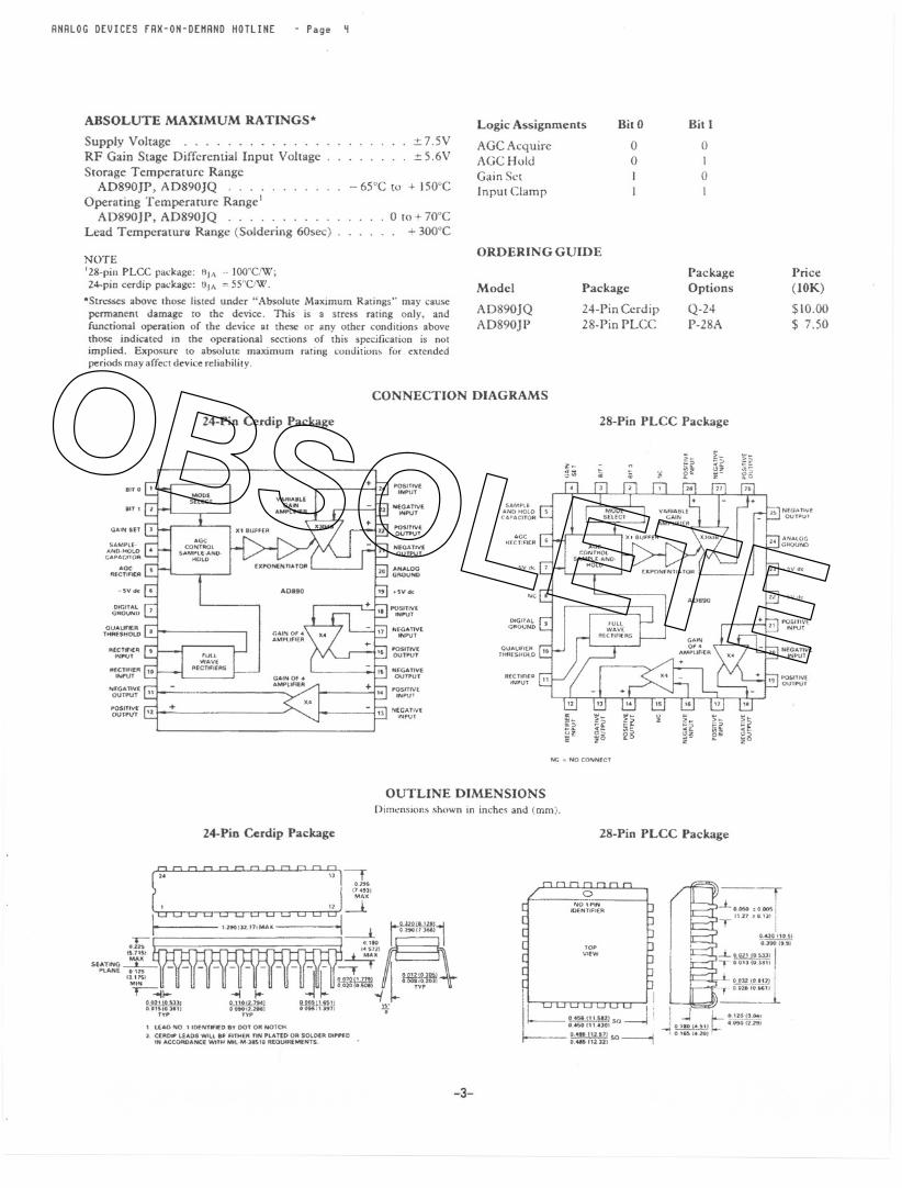
CONNECTION DIAGRAMS
24-PinCerdip Package 28-Pin PLCC Package
w.>-. -
;j!Ji. :i"z" " :<- .,- o
:uI PO
NEGATIVE
f:t w I r I Vlfl I I NJii;:E"""'T ,,",OESHEeT
POSITIVEOUTI>UT
KE.g,," I,211 NJ;:'
20' - SV d<
.SVd<NC
POsmY<INPUT
g't};\ I I fUll r I I .R p?:a'", N\VE
WAV'
..1 :GUAL>r' J A"';:';'ER\/ "'-GATIVE""'SHOlO,. "INPUT
/'1 +.., N'GATIVE
R. iiiOUTPUT
""i:."'E
,,' NZJ\V' . . 5 u'Ii.
w!;
:;z 5..0 t: ..
ti c.5
::>:iJ <.0::>
!!'- \:0 z 1i'°
NO.NO CONN'CT
OUTLINE DIMENSIONS
[)imnsions shown in inches and (mm).
24-Pio Cerdip Package 28.Pin PLCC Package
Logic Assignments HitO Bit 1
AGC Acquire 0 0AGC Hold 0 IGain SCt I ()
Input Clamp I 1
OBSOLETE
ANALOGDEVICES fAX-ON-DEMAND HOTLINE - Page 5
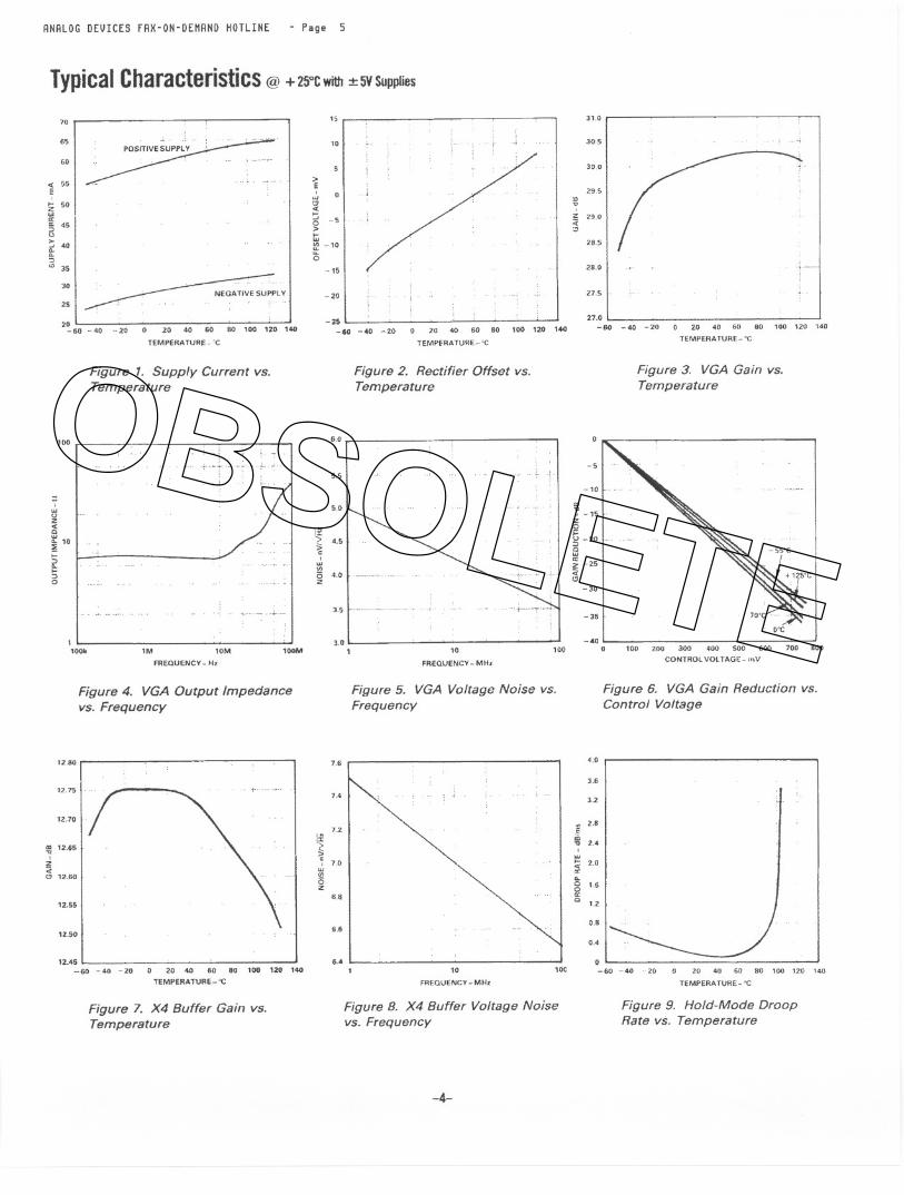
TypicalCharacteristics@ +25OCwithj: 5YSupplies
"0
65
60
" 55E
~50uJa:5 45u~ 40..!!;V> 35
30NEGATIVE SUPPLY
25
20- 60 ...40 .. 20 20 40 60 80 100 1l0 140
TEMPERATURE. "C
Figure 1. Supply Current vs.Temperature
100
. "
~..Q~ 10;!...::1~::10
I100k 1M 10M
FREQUENCY-Hz
Figure 4. VGA Output Impedancevs. Frequency
12.80
12.75
12.70
!g 12.65I
Z«'" 12.&0
12.55
12.50
12.45...60 -40 -20 0 20 40 60 80 100 120 140
TEMPERATURE-'C
Figure 7. X4 Buffer Gain V$.Temperature
100M
15
10
;-E;
uJ'""...5 ..5;-...~ .100
-15
..20
-lS-eo -40-20 0 20 4G 60 80
TEMPfRATURE.'C
100 120 140
Figure 2. Rectifier Offset V5.Temperature
6.0
5.5
5.0
IX'> 4.5~.;,5 '0z
3.5
3.01 10
FREQUENCY - MHl
Figure 5. VGA Voltage Noise vs.Frequency
100
no
30.5
30.0
29.5.,"
Z 29.0d''"
28.5
28.0
27.5
27.0
-60 -40 -20 0 20 40 60 80 100 120 140
TEMPERATURE-'C
Figure 3. VGA Gain Ys.Temperature
-5
-10
'"".; .150;::g -200wa:Z -25"'"
-30
-35
o'C
-40a 200 300 400 500 600
CONTROL VOLTAGE - mV
700 800100
Figure 6. VGA Gain Reduction vs.Control Voltage
7.&
7.4
7.2i:i:'c;-~ 70wIS>isz
6.8
&.8
6,4 -1 10
FREQUENCY - MHl
Figure 8. X4 Buffer Voltage NoiseV5. Frequency
-4-
~---
20 40 &0 80 100 120 140
TEMPERATURE - "C
Figure 9. Hold-Mode DroopRate Y5. Temperature
4.0
3.6
3.2
2.8"Iii2.4,
2.0a:..C 1.6ca:0
1.2
0.8
0.4
0100 -60 -40 . 20
OBSOLETE
ANALOG DEVICES FAX-ON-DEMANDHOTLINE 6- Page
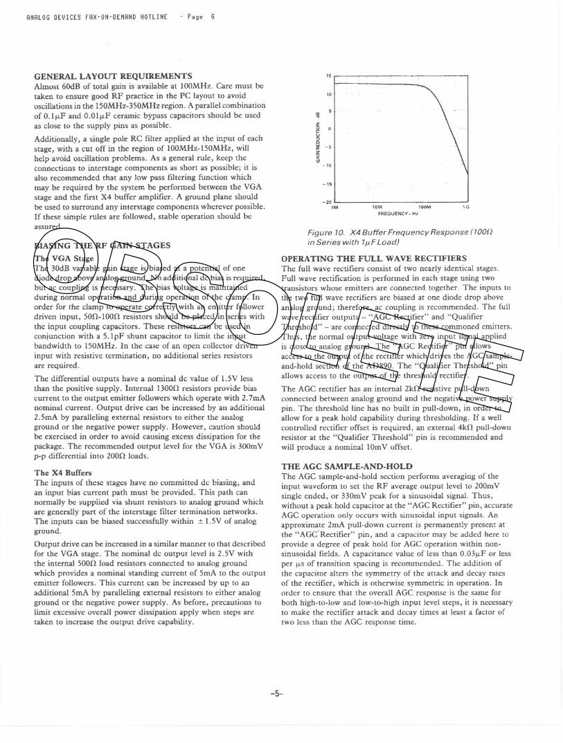
GENERAL LAYOUT REQUIREMENTSAlmost 6OdB of tOtal gain is available at lOOMHz. Care must betaken to ensure good RF practice in the PC layout to avoidoscillations in the 150MHz-350MHz region. A parallel combinationofO.lfLF and O.OIJ.LFceramic bypass capacitors should be usedas close to the supply pins as possible.
Additionally, a single pole RC filter applied at the inpUt of eachstage, with a cut off in the region of 1O0MHz-150MHz, willhelp avoid oscillation problems. As a general rule, keep theconnections to imerstage componcnts as short as possible; it isalso recommended that any low pass filtering function whichmay bc required by the system be performed between the VGAstage and the first X4 buffer amplifier. A ground plane shouldbe used to surround any interstage components wherever possible.If these simple rules are followed, stable operation should beassured.
BIASING THE RF GAIN STAGES
The VGA StageThe 30dB variable gain stage is biased at a potential of onediode drop above analog ground. No additional dc bias is required,bUt ac coupling is necessary. The bias voltage is maintainedduring normal operation and during operation of the clamp. Inorder for the clamp to operate correctly with an emitter followerdriven input, 50H-lOOn resistors should be placed in series withthe inpUt coupling capacitors. These resistors can be used inconjunction with a 5.1pF shunt capacitor to limit the inpUtbandwidth to 150MHz. In the case of an open collector driveninpUt with resistive termination, no additional series resistorsare required.
The differential outputs have a nominal dc value of 1.5V lessthan the positive supply. Internal 1300n resistors provide biascurrent to the output emitter followers which operate with 2.7mAnominal current. Output drive can be increased by an additional2.5mA by paralleling external resistors to either the analogground or the negative power supply. However, caution shouldbe exercised in order to avoid causing excess dissipation for thepackage. The recommended output level for the VGA is 300mVp-p differential into 200n loads.
The X4 BuffersThe inputs of these stages have no committed dc biasing, andan input bias current path must be provided. This path cannormally be supplied via shunt resistors to analog ground whichare generally part of the interstage filter termination networks.The inputs can be biased successfully within :t:1.5V of analogground.
Output drive can be increased in a similar manner to that describedfor the VGA stage. The nominal dc output level is 2.5V withthe internal soon load resistors connected to analog groundwhich provides a nominal standing current of SmA to the outputemitter followers. This current can be increased by up to anadditional SmA by paralleling external resistors to either analogground or the negative power supply. As before, precautions tolimit excessive overaH power dissipation apply when steps aretaken to increase the output drive capability.
15
10
~
is 0;::V:J0::! - 5Z<i<3
-10
-15
-201M 10M 100M
FREQUENCY -H7
1G
Figure 10. X4 Buffer Frequency Response (toonin Series with 1p.F Load)
OPERATING THE FULL WAVE RECTIFIERSThe full wave rectifiers consist of two nearly identical stages.Full wave rectification is performed in each stage using twotransistors whose emitters are connected together. The inputs tothe two full wave rectifiers are biased at one diode drop aboveanalog ground; therefore, ac coupling is recommended. The fullwave rectifier oUtputs - "AGe Rectifier" and "QualifierThreshold" - arc connected directly to these commoned emitters.Thus, the normal output voltage with zero inpUt signal appliedis close to analog ground. The" AGe Rectifier" pin allowsaccess to the oUtpUt of the rectifier which drives the AGC sample-and-hold section of the AD890. The "Qualifier Threshold" pinallows access to the oUtpUt of the threshold rectifier.
The AGe rectifier has an internal 2kD resistive pull-downconnected between analog ground and the negative power supplypin. The threshold line has no built in pull-down, in order toallow for a peak hold capability during thresholding. If a wellcontrolled rectifier offset is required, an external 4kH pull-downresistor at the "Qualifier Threshold" pin is recommended andwill produce a nominal 10mV offset.
THE AGC SAMPLE-AND-HOLDThe AGC sample-and-hold section performs averaging of theinput waveform to set the RF average output level to 200mVsingle ended, or 330mV peak t'Ora sinusoidal signal. Thus,without a peak hold capacitOr at the "AGC Rectifier" pin, accurateAGC operation only occurs with sinusoidal inpUt signals. Anapproximate 2mA pull-down current is permanently present atthe "AGC"Rectifier" pin, and a capacitor may be added here toprovide a degree of peak hold for AGC operation within 000-sinusoidal fields. A capacitance value of less than 0.O3J.LFor lessper fLSof transition spacing is recommended. The addition ofthe capacitor alters the symmetry of the attack and decay ratesof the rectifier, which is otherwise symmetric in operation. Inorder to ensure that the overall AGC response is the same forboth high-to-Iow and low-to-high input level steps, it is necessaryto make the rectifier anack and decay times at least a factor oftwo less than the AGe response time.
-5-
----
OBSOLETE
ANALOG DEVICES FAX-ON-DEMANDHOTLINE - Page 7
The AGC acquire time is approximately 1j.LSper 1O0DpFof holdcapacitor. A low leakage variety of hold capacitor, such as asilver mica, is necessary to ensure low droop rates. The "GainSet" pin should be tied to analog ground if not used, in order toprevent excessive leakage which would otherwise affect the holdperformance.
The AGC comrol potential is present at the "Sample-and-HoldCapacitor" pin. If control over open-loop gain is desired, basedon AGC comro! potentialsobtained during trial AGCoperations,a FET inpUt op amp should be used to buffer this node inorder to avoid distUrbing the hold operation.
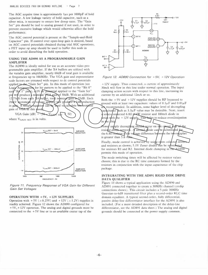
USING THE AD890 AS A PROGRAMMABLE GAINAMPLIFIERThe AD890 is ideally suited for use as an accurate video pro-grammable gain amplifier. If the X4 buffers are utilized withthe variable gain amplifier, nearly 6DdB of total gain is availableat frequenciesup to 1O0MHz.The VGA gain and exponemiatorscale factors are trimmed with respect to de control potentialsapplied to the "Gain Set" pin. In this mode of operation (seeLogic Assignments for bit pattern to be applied to the "Bit 0"and "Bit I" pins), a OVdc potential applied to the "Gain Set"pin will produce a nominal VGA gain of 30dB. With an additional12.75dB from each X4 buffer, tOtal nominal gain is SSdB. Each2DmV increment of voltage applied will produce a IdB reductionin gain. A simple equation can be used to calculate the nominalgain of VGA in this mode:
VGA Gain(dB) = (30 - VGAIN SET X 50)
where VGAINSETis in volls.
30V HSET ~ OmV OdBGAIN
REDUCTION
I!! 20
Z0tg 10::!z"<:J
V""H SET .~ <OOmV 20dBGAINREDUCTION
V".", SET " SOOmV .OdaGAINREDUCTION10
100k 1M 10M
FREQUENCY." Hz
100M
Figure ". Frequency Response of VGA Gain for DifferentGain Set Voltages
OPERATION WITH +5V, +12V SUPPLIESOperation with +-5V (:::D.25V)and +-12V(= 1.2V)supplies isreadily achieved. Figure 12 shows the AD890 configured for+-SV, + 12V operation. The analog and digital grounds must beconnected to the +-5V line or 10 an available center tap of the
RS6.8n
+12V
olZV ..L CI ..I.. C2
~O."'f ~OOI"f 1+11VA3.1' .I' A4 (IS
SkU c; ~ SkI! .
CRI11'14001
+SV
AI39k"
A239kU
C3 ..L C4
~OII'F ~0.01"F
AO890
v"
Figure 12. AD890 Connection for + 5V, f- 12V Operation
+-12V supply. Thus connected, a current. of approximately30mA will flow in this line under normal operation. The input
clamping action occurs with respect to this line, increasing itscurrent by an additional J2mA or so.
Both the +-SV and +-J2V supplies should be RF bypassed toground with at ]cast two capacitors: values ofO.lf-lF and O.OIj.LFare recommended. In addition, some higher level of decouplingcapacitance such as 3.3f-lF value may be desirable. Next, inserta series-connected 6.8!! l/4W resistor and lOOmA diode in
series with the + 12V supply. This helps to reduce overdissipationin the chip.
Power supply decoupling should occur on the circuit side of theresistor-diode network. A second diode can be substituted for
the 6.8!! resistor if the voltage difference between the two suppliesis greater than 5.6 volts.
Finally, mode control is achieved by using open collector driversand resistors as shown; 5.1V Zener diodes can be substitUtedfor resistors R I and R2. Internal diode clamping in the AD890permits this mode of operation.
The mode switching times will be affected by resistor valueschosen; this is due to the RC time constants formed by theresistors in conjunction with the input capacitance of the chippackage.
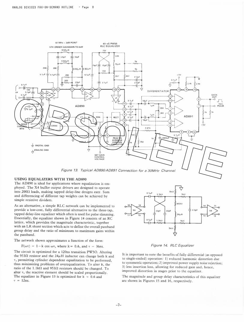
INTEGRATING WITH THE AD891 RIGID DISK DRIVEDATA QUALIFIERFigure 13 shows a typical application using the AD890 and/\D891 connected together to create a 30MHz channel (cerdipconnections shown). This circuit includes a 5-pole 30MHzGaussian-to-6dB transitional filter plus a se<.:ond-orderRLC timedomain equalizer. A typical second-order, fully differemial,passive delay-line differenriator interface for the AD891 is alsoincluded. (For a more detailed description of the delay-linedifferentiator, see the AD891 data sheet.) The analog and digitalgrounds should be connecl.ed at the power supply common.
-6-
OBSOLETE
ANALOGDEVICES FAX-ON-DEHAND HOTLINE - Page B
50 MHz - 3dB POINT 40 nS PWSOAlC EQUALIZER5TH ORDER GAUSSIAN-TO-tidB
0 62,.H 133
3.9pf
062,.>1
10pf
11SPF£:~
OHZ"H~O82"H T ~::f I0-l,.f ~-
2Zpf ! T 1/f' 0 '"F
200 200
1o..,..0.'",
~ DIGITAL GND
\7 "'N"'LOG GIIID
636
5k
fZ,.H
s.
661.>v
66}22pf
DATAOuT
(8'> r--o TL, ","-
J-
.
-- ! ---0 PUlSE
1k "
.-sv
Figure 13- Typical AD890/AD891 Connection for a 30MHz Channel
USING EQUALIZERS WITH THE AD890The AD890 is ideal for applications where equalization is em-ployed. The X4 buffer oUtpUt drivers are designed to operateinto 200n loads, making tapped delay-line designs easy. Sumand differencing of different rap weights can be achieved bysimple resistive dividers.
As an alternative, a simple RLC network can be implemented toprovide a low-cost, fully differential alternative to the three-tap,tapped delay-line equalizer which often is used for pulse slimming.Essentially, the equalizer shown in Figure 14 consists of an RClanice, which provides the magnitUde characteristic, togetherwith an LR shunt section which acts to define the overall passbandgroup delay and the ratio of minimum to maximum gains withinthe passband.
The network shown approximates a function of the form:
F«(oJ'T)"" l-kcos(j)'T,wherek"" O.6,andT = 36ns-
The circuit is optimized for a l20ns transition PW50. Alteringthe 953fl resistor and the 24J.LHinductor can change both k andT, permitting cylinder dependent equalization to be perfcJrmed,thus minimizing problems of overequalization. To alter k, theratio of the 1.lkH and 95311resistors should be changed. Toalter T, the reactive element should be scaled proportionally.The equalizer in Figure 13 is optimized for k '= 0.6 and'T = J2ns.
-- ~--
18
17
Figure 14. RLC Equalizer
It is important to note the benefits of fully differential (as opposedto single-ended) operation: I) reduced harmonic distortion dueto symmetric operation; 2) improved power supply noise rejection;3) less insertion loss, allowing for reduced gain and, hence,improved distortion in stages prior to the equalizer.
The magnitude and group delay characteristics of this equalizerarc shown in Figures 15 and 16, respectively.
-7-
SkU1kU'O.lF ,n"
9S311
122"fT.
24"H
uk" I
Sk"
OBSOLETE
ANALOGDEVICES fAX-ON-DEMAND HOTLINE - Page 9
'"",~o"
l !
.-2
-4
-6100k 1M 10M
FREQUENCY- H.100M
Figure 15. RLC Equalizer Magnitude Response
~c;>-..
....I!:-10...:::00a:;" -20 ,.
Figure 16.
20
10
°
..30
...40100k 1M 10M
FREQUENCY. Hz
100M
RLC Equalizer Group Delay Response
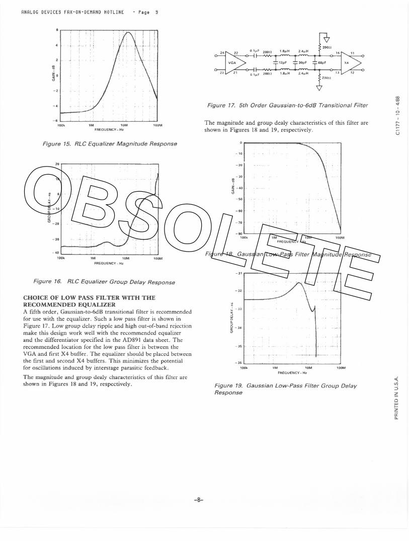
CHOICE OF LOW PASS FILTER WITH THERECOMMENDED EQUALIZERA fifth order, Gaussian-ro-6dB transitional filter is recommendedfor use with the equalizer. Such a low pass filter is shown inFigure 17. Low group delay ripple and high out-of-band rejectionmake this design work well with the recommended equalizerand the differentiator specified in the AD89] data sheet. Therecommended location for the low pass filter is between theVGA and first X4 buffer. The equalizer should be placed betweenIhe fIrst and second X4 buffers. This minimizes the potentialfor oscillations induced by imerslage parasitic feedback.
The magnitude and group dealy characteristics of Ibis filter areshown in Figures ]8 and 19, respectively.
---~
24
23
ZOOt!1.8"H 24"H
200H
coco<t
I0
I"-"-~
u
Figure 17. 5th Order Gaussian-to-6dB Transitional Filter
The magnitUde and group dealy characteristics of this filter areshown in Figures 18 and 19, respectively.
0
- 10
-20
-30'"",~-40"
-50
-&0
- 70
-80100k
Figure 18. Gaussian Low-Pass Filter Magnitude Response
1M 10MFREQUENCY H.
100M
-31
-32
~
, -33>-"~"...:::00-34a:"
-35
-3"100k 1M 10M
FREQuENCY. H.100M
<ien::izCIuuI-~c:::0...
Figure 19. Gaussian Low-Pass Filter Group DelayResponse
-8-
--
OBSOLETE