Embed Size (px)
Citation preview

MIX
ER
S -
SM
T
1
For price, delivery and to place orders: Hittite Microwave Corporation, 2 Elizabeth Drive, Chelmsford, MA 01824Phone: 978-250-3343 Fax: 978-250-3373 Order On-line at www.hittite.com
Application Support: Phone: 978-250-3343 or [email protected]
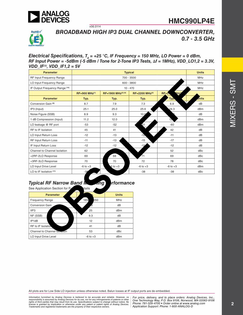
HMC990LP4EBROADBAND HIGH IP3 DUAL CHANNEL DOWNCONVERTER,
0.7 - 3.5 GHz
v06.0114
All plots are for Low Side LO injection unless otherwise noted. Balun losses at IF output ports are de-embedded.
General Description
Features
Functional Diagram
Typical ApplicationsThe HMC990LP4E is Ideal for:
• Multiband/Multi-standard Cellular BTS Diversity Receivers
• GSM & 3G & LTE/WiMAX/4G
• MIMO Infrastructure Receivers
• Wideband Radio Receivers
• Multiband Basestations & Repeaters
Broadband Operation with no external matching
Industry’s Most Compact Solution, 4x4 mm2 QFN Package
High-side and Low-side LO injection Operation
Wide IF Frequency Range
High Input IP3 of +25.6dBm @ 2200 MHz
Power Conversion Gain of 7.9 dB
Input P1dB of 12 dBm
SSB Noise Figure of 9 dB
55 dBc Channel-to-Channel Isolation
Dedicated Enable Pins for IF & LO amplifiers
Single-ended RF & LO input ports
The HMC990LP4E is a high linearity, dual channel down-converting mixer optimized for multi-standard diversity receiver applications that require low power consump-tion and small size. The HMC990LP4E features new wideband limiting LO amplifiers to achieve an unprec-edented RF bandwidth of 700 MHz to 3500 MHz. Unlike conventional narrow-band downconverter RFICs, the HMC990LP4E supports both high-side and low-side LO injection over the entire RF frequency band. The RF and LO input ports are internally matched to 50Ω.
The HMC990LP4E integrates LO and IF amplifiers with enable functions, LO and RF baluns and high linear-ity passive mixer cores with bias control interface. The balanced passive mixer combined with high-linearity IF amplifier architecture of HMC990LP4E provides excel-lent LO-to-RF, LO-to-IF, and RF-to-IF isolations. The HMC990LP4E provides a very low noise figure of 9dB, and high IIP3 of +25.6dBm allowing device to be used in demanding wideband applications. The HMC990LP4E’s input IP3 can be further improved by external matching for narrow-band applications. The HMC990LP4E has typical less than 1.5W power consumption which can be optimized through external bias control pins. The HMC990LP4E also features a very fast enable control interface for to be used for power saving in Time Division Duplex (TDD) applications. The HMC990LP4E is housed in a RoHS compliant 4x4 mm2 leadless QFN package.
Information furnished by Analog Devices is believed to be accurate and reliable. However, no responsibility is assumed by Analog Devices for its use, nor for any infringements of patents or other rights of third parties that may result from its use. Specifications subject to change without notice. No license is granted by implication or otherwise under any patent or patent rights of Analog Devices. Trademarks and registered trademarks are the property of their respective owners.
For price, delivery, and to place orders: Analog Devices, Inc., One Technology Way, P.O. Box 9106, Norwood, MA 02062-9106 Phone: 781-329-4700 • Order online at www.analog.com Application Support: Phone: 1-800-ANALOG-D
OBSOLETE
MIX
ER
S -
SM
T
2For price, delivery and to place orders: Hittite Microwave Corporation, 2 Elizabeth Drive, Chelmsford, MA 01824
Phone: 978-250-3343 Fax: 978-250-3373 Order On-line at www.hittite.comApplication Support: Phone: 978-250-3343 or [email protected]
All plots are for Low Side LO injection unless otherwise noted. Balun losses at IF output ports are de-embedded.
HMC990LP4EBROADBAND HIGH IP3 DUAL CHANNEL DOWNCONVERTER,
0.7 - 3.5 GHz
v06.0114
Parameter Typical Units
RF Input Frequency Range 700 - 3500 MHz
LO Input Frequency Range 600 - 3800 MHz
IF Output Frequency Range [10] 10 - 470 MHz
RF=900 MHz[1] RF=1900 MHz[2] [9] RF=2200 MHz[2] RF=2700 MHz[2]
Parameter Typ. Typ. Typ. Typ. Units
Conversion Gain [8] 8.7 7.9 7.3 6.9 dB
IP3 (Input) 25.1 25.0 25.6 24.3 dBm
Noise Figure (SSB) 8.9 9.3 10.0 10.3 dB
1 dB Compression (Input) 11.2 12.0 12.0 12.3 dBm
LO leakage @ RF port -53 -52 -51 -60 dBm
RF to IF Isolation 45 41 42 42 dB
LO Input Return Loss -12 -13 -12 -11 dB
RF Input Return Loss -11 -13 -15 -17 dB
IF Input Return Loss -12 -12 -12 -12 dB
Channel to Channel Isolation 62 53 52 52 dBc
+2RF-2LO Response 69 68 71 69 dBc
+3RF-3LO Response 70 70 72 78 dBc
LO Input Drive Level -6 to +3 -6 to +3 -6 to +3 -6 to +3 dBm
LO to IF Isolation [11] -38 -38 -38 -38 dBc
Electrical Specifications, TA = +25 °C, IF Frequency = 150 MHz, LO Power = 0 dBm, RF Input Power = -5dBm (-5 dBm / Tone for 2-Tone IP3 Tests, ∆f = 1MHz), VDD_LO1,2 = 3.3V, VDD_IF[3], VDD_IF1,2 = 5V
Parameter Typ. Units
Frequency Range 1850 - 2050 MHz
Conversion Gain 7.9 dB
IIP3 25 dBm
NF (SSB) 9.3 dB
IP1dB 12 dBm
RF to IF Isolation 41 dB
Channel to Channel Isolation 53 dBc
LO Input Drive Level -6 to +3 dBm
Typical RF Narrow Band Matching PerformanceSee Application Section for Further Details
Information furnished by Analog Devices is believed to be accurate and reliable. However, no responsibility is assumed by Analog Devices for its use, nor for any infringements of patents or other rights of third parties that may result from its use. Specifications subject to change without notice. No license is granted by implication or otherwise under any patent or patent rights of Analog Devices. Trademarks and registered trademarks are the property of their respective owners.
For price, delivery, and to place orders: Analog Devices, Inc., One Technology Way, P.O. Box 9106, Norwood, MA 02062-9106 Phone: 781-329-4700 • Order online at www.analog.com Application Support: Phone: 1-800-ANALOG-D
OBSOLETE

MIX
ER
S -
SM
T
3
For price, delivery and to place orders: Hittite Microwave Corporation, 2 Elizabeth Drive, Chelmsford, MA 01824Phone: 978-250-3343 Fax: 978-250-3373 Order On-line at www.hittite.com
Application Support: Phone: 978-250-3343 or [email protected]
HMC990LP4EBROADBAND HIGH IP3 DUAL CHANNEL DOWNCONVERTER,
0.7 - 3.5 GHz
v06.0114
All plots are for Low Side LO injection unless otherwise noted. Balun losses at IF output ports are de-embedded.
DC Power Supply Specifications,Parameter Conditions Min. Typ. Max. Units.
IF Supply Voltage (VDD_IF[3], VDD_IF1,2[4]) +4.75 +5 +5.25 V
LO Supply Volltage (VDD_LO1,2) +3.15 +3.3 +3.45 V
IF Amplifier Supply Current when enabled
VDD_IF[3] 148 mA
VDD_IF1[4] + VDD_IF2[4] 24 mA
VCS1[5] + VCS2[5] 3 mA
IF Amplifier Supply Current when disabled
VDD_IF[3] 0 mA
VDD_IF1[4] + VDD_IF2[4] 3 mA
VCS1[5] + VCS2[5] 4 mA
LO Amplifier Supply Current when enabledVDD_LO1,2 170 mA
LO_BIAS1[6] + LO_BIAS2[6] 4.6 mA
LO Amplifier Supply Current when disabledVDD_LO1,2 4 mA
LO_BIAS1[6] + LO_BIAS2[6] 5.4 mA
Vgate Bias when enabled VGATE1 + VGATE2 3.6 mA
Vgate Bias when disabled VGATE1 + VGATE2 2 mA
Information furnished by Analog Devices is believed to be accurate and reliable. However, no responsibility is assumed by Analog Devices for its use, nor for any infringements of patents or other rights of third parties that may result from its use. Specifications subject to change without notice. No license is granted by implication or otherwise under any patent or patent rights of Analog Devices. Trademarks and registered trademarks are the property of their respective owners.
For price, delivery, and to place orders: Analog Devices, Inc., One Technology Way, P.O. Box 9106, Norwood, MA 02062-9106 Phone: 781-329-4700 • Order online at www.analog.com Application Support: Phone: 1-800-ANALOG-D
OBSOLETE
MIX
ER
S -
SM
T
4For price, delivery and to place orders: Hittite Microwave Corporation, 2 Elizabeth Drive, Chelmsford, MA 01824
Phone: 978-250-3343 Fax: 978-250-3373 Order On-line at www.hittite.comApplication Support: Phone: 978-250-3343 or [email protected]
All plots are for Low Side LO injection unless otherwise noted. Balun losses at IF output ports are de-embedded.
HMC990LP4EBROADBAND HIGH IP3 DUAL CHANNEL DOWNCONVERTER,
0.7 - 3.5 GHz
v06.0114
LO/IF, Enable/Disable Interface Specifications,Parameter Conditions Min. Typ. Max. Units.
LO_EN High Level LO Amplifier Disabled +3 +5 V
LO_EN Low Level LO Amplifier Enabled 0 0 +1 V
IFA1_EN / IFA2_EN High Level Channel1/2 IF Amplifier Disabled +3 +5 5 V
IFA1_EN / IFA2_EN Low Level Channel1/2 IF Amplifier Enabled 0 0 +1 V
Enable Settling Time[7] 30 ns
Disable Settling Time[7] 130 ns
[3] Supply voltage for IF amplifiers through choke inductors. See application circuit.[1] High side LO injection, VGATE1,2 = 5.0V [2] Low side LO injection, VGATE1,2 = 4.8V
[4] Supply voltage for bias circuit of IF amplifiers. See application circuit.[5] Bias Control pins for IF amplifiers. See application circuit.[6] Bias Control pins for LO amplifier. See application circuit.[7] Remove bypass capacitors on LO_EN and IFA1,2_EN pins for given settling times. See application circuit.[8] Balun losses at IF output port are de-embedded.[9] 1900 MHz matching band covers 1850 - 2050 MHz[10] The part is characterized with IF = 150 MHz. External matching maybe needed for diffrent IF frequencies.[11] LO Power is 0 dBm, RF Power is -5 dBm.
Information furnished by Analog Devices is believed to be accurate and reliable. However, no responsibility is assumed by Analog Devices for its use, nor for any infringements of patents or other rights of third parties that may result from its use. Specifications subject to change without notice. No license is granted by implication or otherwise under any patent or patent rights of Analog Devices. Trademarks and registered trademarks are the property of their respective owners.
For price, delivery, and to place orders: Analog Devices, Inc., One Technology Way, P.O. Box 9106, Norwood, MA 02062-9106 Phone: 781-329-4700 • Order online at www.analog.com Application Support: Phone: 1-800-ANALOG-D
OBSOLETE

MIX
ER
S -
SM
T
5
For price, delivery and to place orders: Hittite Microwave Corporation, 2 Elizabeth Drive, Chelmsford, MA 01824Phone: 978-250-3343 Fax: 978-250-3373 Order On-line at www.hittite.com
Application Support: Phone: 978-250-3343 or [email protected]
HMC990LP4EBROADBAND HIGH IP3 DUAL CHANNEL DOWNCONVERTER,
0.7 - 3.5 GHz
v06.0114
All plots are for Low Side LO injection unless otherwise noted. Balun losses at IF output ports are de-embedded.
40
50
60
70
80
90
100
0.7 1.1 1.5 1.9 2.3 2.7 3.1 3.5
4.7V4.8V
4.9V5.0V
+3R
F-3
LO
RE
SP
ON
SE
(dB
c)
FREQUENCY (GHz)
+3RF -3LO Response vs. VGATE[1]
40
50
60
70
80
90
100
0.7 1.1 1.5 1.9 2.3 2.7 3.1 3.5
4.7V4.8V
4.9V5.0V
+2R
F-2
LO
RE
SP
ON
SE
(dB
c)
FREQUENCY (GHz)
+2RF -2LO Response vs. VGATE[1]
5
7
9
11
13
15
0.7 1.1 1.5 1.9 2.3 2.7 3.1 3.5
4.7 V4.8 V4.9 V5.0 V
NO
ISE
FIG
UR
E (
dB
)
FREQUENCY (GHz)
Noise Figure vs. VGATE[1]
15
17
19
21
23
25
27
29
31
4.7 V4.8 V4.9 V5 .0V
0.7 1.1 1.5 1.9 2.3 2.7 3.1 3.5
IIP
3(d
Bm
)
FREQUENCY (GHz)
Input IP3 vs. VGATE[1]
0
2
4
6
8
10
12
4.7 V
4.8 V
4.9 V
5.0 V
0.7 1.1 1.5 1.9 2.3 2.7 3.1 3.5
CO
NV
ER
SIO
N G
AIN
(dB
)
FREQUENCY (GHz)
Conversion Gain vs. VGATE[1]
[1] VGATE is bias voltage for passive mixer cores (VGATE1 and VGATE2 pins). Refer to pin description table.
Information furnished by Analog Devices is believed to be accurate and reliable. However, no responsibility is assumed by Analog Devices for its use, nor for any infringements of patents or other rights of third parties that may result from its use. Specifications subject to change without notice. No license is granted by implication or otherwise under any patent or patent rights of Analog Devices. Trademarks and registered trademarks are the property of their respective owners.
For price, delivery, and to place orders: Analog Devices, Inc., One Technology Way, P.O. Box 9106, Norwood, MA 02062-9106 Phone: 781-329-4700 • Order online at www.analog.com Application Support: Phone: 1-800-ANALOG-D
OBSOLETE
MIX
ER
S -
SM
T
6For price, delivery and to place orders: Hittite Microwave Corporation, 2 Elizabeth Drive, Chelmsford, MA 01824
Phone: 978-250-3343 Fax: 978-250-3373 Order On-line at www.hittite.comApplication Support: Phone: 978-250-3343 or [email protected]
All plots are for Low Side LO injection unless otherwise noted. Balun losses at IF output ports are de-embedded.
HMC990LP4EBROADBAND HIGH IP3 DUAL CHANNEL DOWNCONVERTER,
0.7 - 3.5 GHz
v06.0114
0
2
4
6
8
10
12
High Side LO
Low Side LO
0.7 1.1 1.5 1.9 2.3 2.7 3.1 3.5
CO
NV
ER
SIO
N G
AIN
(dB
)
FREQUENCY (GHz)
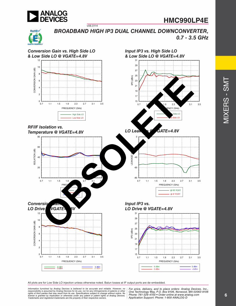
Conversion Gain vs. High Side LO & Low Side LO @ VGATE=4.8V
15
17
19
21
23
25
27
29
31
0.7 1.1 1.5 1.9 2.3 2.7 3.1 3.5
High Side LO
Low Side LO
IIP
3 (
dB
m)
FREQUENCY (GHz)
Input IP3 vs. High Side LO & Low Side LO @ VGATE=4.8V
15
17
19
21
23
25
27
29
31
0.7 1.1 1.5 1.9 2.3 2.7 3.1 3.5
-6 dBm
-3 dBm
0 dBm
+3dBm
IIP
3 (
dB
m)
FREQUENCY (GHz)
Input IP3 vs.LO Drive @ VGATE=4.8V
0
2
4
6
8
10
12
-6 dBm -3 dBm
0 dBm+3 dBm
0.7 1.1 1.5 1.9 2.3 2.7 3.1 3.5
CO
NV
ER
SIO
N G
AIN
(dB
)
FREQUENCY (GHz)
Conversion Gain vs.LO Drive @ VGATE=4.8V
RF/IF Isolation vs.Temperature @ VGATE=4.8V
0
20
40
60
80
0.7 1.1 1.5 1.9 2.3 2.7 3.1 3.5
+25 C+85 C-40 C
ISO
LA
TIO
N (
dB
)
FREQUENCY (GHz)
LO Leakage @ VGATE=4.8V
-80
-60
-40
-20
0
0.7 1.1 1.5 1.9 2.3 2.7 3.1 3.5
@ RF PORT
@ IF PORT
LE
AK
AG
E (
dB
m)
FREQUENCY (GHz)
Information furnished by Analog Devices is believed to be accurate and reliable. However, no responsibility is assumed by Analog Devices for its use, nor for any infringements of patents or other rights of third parties that may result from its use. Specifications subject to change without notice. No license is granted by implication or otherwise under any patent or patent rights of Analog Devices. Trademarks and registered trademarks are the property of their respective owners.
For price, delivery, and to place orders: Analog Devices, Inc., One Technology Way, P.O. Box 9106, Norwood, MA 02062-9106 Phone: 781-329-4700 • Order online at www.analog.com Application Support: Phone: 1-800-ANALOG-D
OBSOLETE
MIX
ER
S -
SM
T
7
For price, delivery and to place orders: Hittite Microwave Corporation, 2 Elizabeth Drive, Chelmsford, MA 01824Phone: 978-250-3343 Fax: 978-250-3373 Order On-line at www.hittite.com
Application Support: Phone: 978-250-3343 or [email protected]
HMC990LP4EBROADBAND HIGH IP3 DUAL CHANNEL DOWNCONVERTER,
0.7 - 3.5 GHz
v06.0114
All plots are for Low Side LO injection unless otherwise noted. Balun losses at IF output ports are de-embedded.
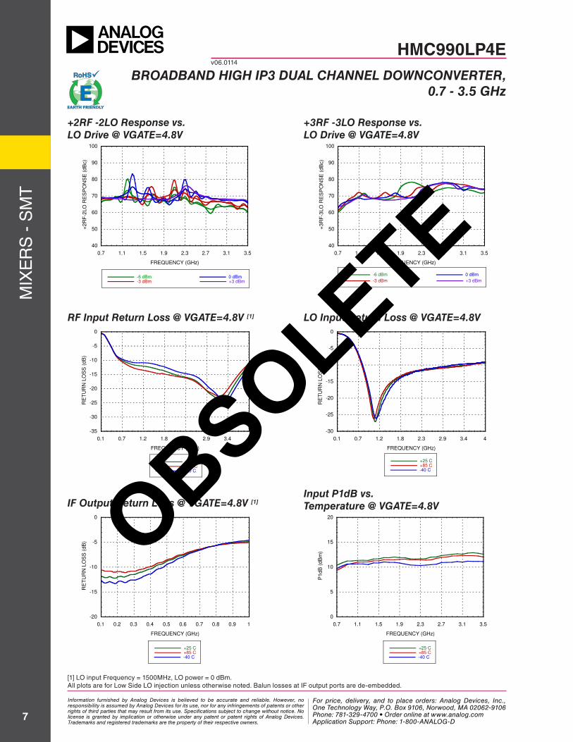
+2RF -2LO Response vs.LO Drive @ VGATE=4.8V
+3RF -3LO Response vs.LO Drive @ VGATE=4.8V
40
50
60
70
80
90
100
0.7 1.1 1.5 1.9 2.3 2.7 3.1 3.5
-6 dBm-3 dBm
0 dBm+3 dBm
+2R
F-2
LO
RE
SP
ON
SE
(dB
c)
FREQUENCY (GHz)
40
50
60
70
80
90
100
0.7 1.1 1.5 1.9 2.3 2.7 3.1 3.5
-6 dBm
-3 dBm
0 dBm
+3 dBm
+3R
F-3
LO
RE
SP
ON
SE
(dB
c)
FREQUENCY (GHz)
-35
-30
-25
-20
-15
-10
-5
0
0.1 0.7 1.2 1.8 2.3 2.9 3.4 4
+25 C+85 C-40 C
RE
TU
RN
LO
SS
(dB
)
FREQUENCY (GHz)
-30
-25
-20
-15
-10
-5
0
0.1 0.7 1.2 1.8 2.3 2.9 3.4 4
+25 C+85 C-40 C
RE
TU
RN
LO
SS
(dB
)
FREQUENCY (GHz)
RF Input Return Loss @ VGATE=4.8V [1] LO Input Return Loss @ VGATE=4.8V
[1] LO input Frequency = 1500MHz, LO power = 0 dBm.
0
5
10
15
20
0.7 1.1 1.5 1.9 2.3 2.7 3.1 3.5
+25 C+85 C-40 C
P1dB
(dB
m)
FREQUENCY (GHz)
Input P1dB vs.Temperature @ VGATE=4.8V
-20
-15
-10
-5
0
0.1 0.2 0.3 0.4 0.5 0.6 0.7 0.8 0.9 1
+25 C+85 C-40 C
RE
TU
RN
LO
SS
(dB
)
FREQUENCY (GHz)
IF Output Return Loss @ VGATE=4.8V [1]
Information furnished by Analog Devices is believed to be accurate and reliable. However, no responsibility is assumed by Analog Devices for its use, nor for any infringements of patents or other rights of third parties that may result from its use. Specifications subject to change without notice. No license is granted by implication or otherwise under any patent or patent rights of Analog Devices. Trademarks and registered trademarks are the property of their respective owners.
For price, delivery, and to place orders: Analog Devices, Inc., One Technology Way, P.O. Box 9106, Norwood, MA 02062-9106 Phone: 781-329-4700 • Order online at www.analog.com Application Support: Phone: 1-800-ANALOG-D
OBSOLETE

MIX
ER
S -
SM
T
8For price, delivery and to place orders: Hittite Microwave Corporation, 2 Elizabeth Drive, Chelmsford, MA 01824
Phone: 978-250-3343 Fax: 978-250-3373 Order On-line at www.hittite.comApplication Support: Phone: 978-250-3343 or [email protected]
All plots are for Low Side LO injection unless otherwise noted. Balun losses at IF output ports are de-embedded.
HMC990LP4EBROADBAND HIGH IP3 DUAL CHANNEL DOWNCONVERTER,
0.7 - 3.5 GHz
v06.0114
Input IP3 vs. Temperature @ VGATE=5.0V
Conversion Gain vs. Temperature @ VGATE=5.0V
15
17
19
21
23
25
27
29
31
0.7 1.1 1.5 1.9 2.3 2.7 3.1 3.5
+25 C
+85 C
-40 C
IIP
3 (
dB
m)
FREQUENCY (GHz)
0
2
4
6
8
10
12
0.7 1.1 1.5 1.9 2.3 2.7 3.1 3.5
+25 C
+85 C
-40 C
CO
NV
ER
SIO
N G
AIN
(dB
)
FREQUENCY (GHz)
+2RF -2LO Response vs. Temperature @ VGATE=5.0V
+3RF -3LO Response vs. Temperature @ VGATE=5.0V
40
50
60
70
80
90
100
0.7 1.1 1.5 1.9 2.3 2.7 3.1 3.5
-40 C
+25 C
+85 C
+3R
F-3
LO
RE
SP
ON
SE
(dB
c)
FREQUENCY (GHz)
40
50
60
70
80
90
100
0.7 1.1 1.5 1.9 2.3 2.7 3.1 3.5
-40 C
+25 C
+85 C
+2R
F-2
LO
RE
SP
ON
SE
(dB
c)
FREQUENCY (GHz)
5
7
9
11
13
15
17
0.7 1.1 1.5 1.9 2.3 2.7 3.1 3.5
+25 C
+85 C
-40 C
NO
ISE
FIG
UR
E (
dB
)
FREQUENCY (GHz)
Noise Figure vs. Temperature @ VGATE=5.0V
Information furnished by Analog Devices is believed to be accurate and reliable. However, no responsibility is assumed by Analog Devices for its use, nor for any infringements of patents or other rights of third parties that may result from its use. Specifications subject to change without notice. No license is granted by implication or otherwise under any patent or patent rights of Analog Devices. Trademarks and registered trademarks are the property of their respective owners.
For price, delivery, and to place orders: Analog Devices, Inc., One Technology Way, P.O. Box 9106, Norwood, MA 02062-9106 Phone: 781-329-4700 • Order online at www.analog.com Application Support: Phone: 1-800-ANALOG-D
OBSOLETE

MIX
ER
S -
SM
T
9
For price, delivery and to place orders: Hittite Microwave Corporation, 2 Elizabeth Drive, Chelmsford, MA 01824Phone: 978-250-3343 Fax: 978-250-3373 Order On-line at www.hittite.com
Application Support: Phone: 978-250-3343 or [email protected]
HMC990LP4EBROADBAND HIGH IP3 DUAL CHANNEL DOWNCONVERTER,
0.7 - 3.5 GHz
v06.0114
All plots are for Low Side LO injection unless otherwise noted. Balun losses at IF output ports are de-embedded.
40
50
60
70
80
90
100
0.7 1.1 1.5 1.9 2.3 2.7 3.1 3.5
-40 C+25 C+85 C
+3R
F-3
LO
RE
SP
ON
SE
(dB
c)
FREQUENCY (GHz)
+3RF -3LO Response vs. Temperature @ VGATE=4.9V
40
50
60
70
80
90
100
0.7 1.1 1.5 1.9 2.3 2.7 3.1 3.5
-40 C+25 C+85 C
+2R
F-2
LO
RE
SP
ON
SE
(dB
c)
FREQUENCY (GHz)
+2RF -2LO Response vs. Temperature @ VGATE=4.9V
15
17
19
21
23
25
27
29
31
0.7 1.1 1.5 1.9 2.3 2.7 3.1 3.5
+25 C+85 C-40 C
IIP
3 (
dB
m)
FREQUENCY (GHz)
Input IP3 vs. Temperature @ VGATE=4.9V
0
2
4
6
8
10
12
0.7 1.1 1.5 1.9 2.3 2.7 3.1 3.5
+25 C+85 C -40 C
CO
NV
ER
SIO
N G
AIN
(dB
)
FREQUENCY (GHz)
Conversion Gain vs. Temperature @ VGATE=4.9V
Noise Figure vs. Temperature @ VGATE=4.9V
5
7
9
11
13
15
17
0.7 1.1 1.5 1.9 2.3 2.7 3.1 3.5
+25 C+85 C-40 C
NO
ISE
FIG
UR
E (
dB
)
FREQUENCY (GHz)
Information furnished by Analog Devices is believed to be accurate and reliable. However, no responsibility is assumed by Analog Devices for its use, nor for any infringements of patents or other rights of third parties that may result from its use. Specifications subject to change without notice. No license is granted by implication or otherwise under any patent or patent rights of Analog Devices. Trademarks and registered trademarks are the property of their respective owners.
For price, delivery, and to place orders: Analog Devices, Inc., One Technology Way, P.O. Box 9106, Norwood, MA 02062-9106 Phone: 781-329-4700 • Order online at www.analog.com Application Support: Phone: 1-800-ANALOG-D
OBSOLETE
MIX
ER
S -
SM
T
10For price, delivery and to place orders: Hittite Microwave Corporation, 2 Elizabeth Drive, Chelmsford, MA 01824
Phone: 978-250-3343 Fax: 978-250-3373 Order On-line at www.hittite.comApplication Support: Phone: 978-250-3343 or [email protected]
All plots are for Low Side LO injection unless otherwise noted. Balun losses at IF output ports are de-embedded.
HMC990LP4EBROADBAND HIGH IP3 DUAL CHANNEL DOWNCONVERTER,
0.7 - 3.5 GHz
v06.0114
15
17
19
21
23
25
27
29
31
0.7 1.1 1.5 1.9 2.3 2.7 3.1 3.5
+25 C+85 C-40 C
IIP
3 (
dB
m)
FREQUENCY (GHz)
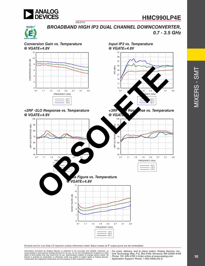
Input IP3 vs. Temperature @ VGATE=4.8V
0
2
4
6
8
10
12
0.7 1.1 1.5 1.9 2.3 2.7 3.1 3.5
+25 C+85 C -40 C
CO
NV
ER
SIO
N G
AIN
(dB
)
FREQUENCY (GHz)
Conversion Gain vs. Temperature @ VGATE=4.8V
40
50
60
70
80
90
100
0.7 1.1 1.5 1.9 2.3 2.7 3.1 3.5
-40 C+25 C+85 C
+2R
F-2
LO
RE
SP
ON
SE
(dB
c)
FREQUENCY (GHz)
+2RF -2LO Response vs. Temperature @ VGATE=4.8V
40
50
60
70
80
90
100
0.7 1.1 1.5 1.9 2.3 2.7 3.1 3.5
-40 C+25 C+85 C
+3R
F-3
LO
RE
SP
ON
SE
(dB
c)
FREQUENCY (GHz)
+3RF -3LO Response vs. Temperature @ VGATE=4.8V
5
7
9
11
13
15
17
0.7 1.1 1.5 1.9 2.3 2.7 3.1 3.5
+25 C+85 C-40 C
NO
ISE
FIG
UR
E (
dB
)
FREQUENCY (GHz)
Noise Figure vs. Temperature @ VGATE=4.8V
Information furnished by Analog Devices is believed to be accurate and reliable. However, no responsibility is assumed by Analog Devices for its use, nor for any infringements of patents or other rights of third parties that may result from its use. Specifications subject to change without notice. No license is granted by implication or otherwise under any patent or patent rights of Analog Devices. Trademarks and registered trademarks are the property of their respective owners.
For price, delivery, and to place orders: Analog Devices, Inc., One Technology Way, P.O. Box 9106, Norwood, MA 02062-9106 Phone: 781-329-4700 • Order online at www.analog.com Application Support: Phone: 1-800-ANALOG-D
OBSOLETE

MIX
ER
S -
SM
T
11
For price, delivery and to place orders: Hittite Microwave Corporation, 2 Elizabeth Drive, Chelmsford, MA 01824Phone: 978-250-3343 Fax: 978-250-3373 Order On-line at www.hittite.com
Application Support: Phone: 978-250-3343 or [email protected]
HMC990LP4EBROADBAND HIGH IP3 DUAL CHANNEL DOWNCONVERTER,
0.7 - 3.5 GHz
v06.0114
All plots are for Low Side LO injection unless otherwise noted. Balun losses at IF output ports are de-embedded.
0
2
4
6
8
10
12
0.7 1.1 1.5 1.9 2.3 2.7 3.1 3.5
+25 C+85 C -40 C
CO
NV
ER
SIO
N G
AIN
(dB
)
FREQUENCY (GHz)
15
17
19
21
23
25
27
29
31
0.7 1.1 1.5 1.9 2.3 2.7 3.1 3.5
+25 C+85 C-40 C
IIP
3 (
dB
m)
FREQUENCY (GHz)
40
50
60
70
80
90
100
0.7 1.1 1.5 1.9 2.3 2.7 3.1 3.5
-40 C+25 C+85 C
+2R
F-2
LO
RE
SP
ON
SE
(dB
c)
FREQUENCY (GHz)
40
50
60
70
80
90
100
0.7 1.1 1.5 1.9 2.3 2.7 3.1 3.5
-40 C+25 C+85 C
+3R
F-3
LO
RE
SP
ON
SE
(dB
c)
FREQUENCY (GHz)
Input IP3 vs. Temperature @ VGATE=4.7V
Conversion Gain vs. Temperature @ VGATE=4.7V
+2RF -2LO Response vs. Temperature@ VGATE=4.7V
+3RF -3LO Response vs. Temperature@ VGATE=4.7V
Noise Figure vs. Temperature @ VGATE=4.7V
5
7
9
11
13
15
17
0.7 1.1 1.5 1.9 2.3 2.7 3.1 3.5
+25 C+85 C-40 C
NO
ISE
FIG
UR
E (
dB
)
FREQUENCY (GHz)
Information furnished by Analog Devices is believed to be accurate and reliable. However, no responsibility is assumed by Analog Devices for its use, nor for any infringements of patents or other rights of third parties that may result from its use. Specifications subject to change without notice. No license is granted by implication or otherwise under any patent or patent rights of Analog Devices. Trademarks and registered trademarks are the property of their respective owners.
For price, delivery, and to place orders: Analog Devices, Inc., One Technology Way, P.O. Box 9106, Norwood, MA 02062-9106 Phone: 781-329-4700 • Order online at www.analog.com Application Support: Phone: 1-800-ANALOG-D
OBSOLETE
MIX
ER
S -
SM
T
12For price, delivery and to place orders: Hittite Microwave Corporation, 2 Elizabeth Drive, Chelmsford, MA 01824
Phone: 978-250-3343 Fax: 978-250-3373 Order On-line at www.hittite.comApplication Support: Phone: 978-250-3343 or [email protected]
All plots are for Low Side LO injection unless otherwise noted. Balun losses at IF output ports are de-embedded.
HMC990LP4EBROADBAND HIGH IP3 DUAL CHANNEL DOWNCONVERTER,
0.7 - 3.5 GHz
v06.0114
Channel to Channel Isolation vs.IF Frequency
40
45
50
55
60
65
70
0.7 1.1 1.5 1.9 2.3 2.7 3.1 3.5
IF=50MHzIF=100MHzIF=150MHzIF=200MHz
IF=250MHzIF=300MHzIF=350MHz
ISO
LA
TIO
N (
dB
c)
FREQUENCY (GHz)
Channel to Channel Isolation vs.VGATE
40
45
50
55
60
65
70
0.7 1.1 1.5 1.9 2.3 2.7 3.1 3.5
4.7V
4.8V
4.9V
5.0V
ISO
LA
TIO
N (
dB
c)
FREQUENCY (GHz)
0
2
4
6
8
10
12
CHANNEL 1
CHANNEL 2
0.7 1.1 1.5 1.9 2.3 2.7 3.1 3.5
CO
NV
ER
SIO
N G
AIN
(dB
)
FREQUENCY (GHz)
Conversion Gain,Channel Matching @ VGATE=4.8V
15
17
19
21
23
25
27
29
31
0.7 1.1 1.5 1.9 2.3 2.7 3.1 3.5
CHANNEL 1CHANNEL 2
IIP
3 (
dB
m)
FREQUENCY (GHz)
Input IP3,Channel Matching @ VGATE=4.8V
15
17
19
21
23
25
27
29
31
0.7 1.1 1.5 1.9 2.3 2.7 3.1 3.5
Vdd_IF=4.75V, Vdd_LO=3.15V
Vdd_IF=5.0V, Vdd_LO=3.3V
Vdd_IF=5.25V, Vdd_LO=3.45V
IIP
3 (
dB
m)
FREQUENCY (GHz)
Input IP3 vs.Vdd @ VGATE=4.8V
0
2
4
6
8
10
12
0.7 1.1 1.5 1.9 2.3 2.7 3.1 3.5
Vdd_IF=4.75V, Vdd_LO=3.15V
Vdd_IF=5.00V, Vdd_LO=3.30V
Vdd_IF=5.25V, Vdd_LO=3.45V
CO
NV
ER
SIO
N G
AIN
(dB
)
FREQUENCY (GHz)
Conversion Gain vs.Vdd @ VGATE=4.8V
Information furnished by Analog Devices is believed to be accurate and reliable. However, no responsibility is assumed by Analog Devices for its use, nor for any infringements of patents or other rights of third parties that may result from its use. Specifications subject to change without notice. No license is granted by implication or otherwise under any patent or patent rights of Analog Devices. Trademarks and registered trademarks are the property of their respective owners.
For price, delivery, and to place orders: Analog Devices, Inc., One Technology Way, P.O. Box 9106, Norwood, MA 02062-9106 Phone: 781-329-4700 • Order online at www.analog.com Application Support: Phone: 1-800-ANALOG-D
OBSOLETE
MIX
ER
S -
SM
T
13
For price, delivery and to place orders: Hittite Microwave Corporation, 2 Elizabeth Drive, Chelmsford, MA 01824Phone: 978-250-3343 Fax: 978-250-3373 Order On-line at www.hittite.com
Application Support: Phone: 978-250-3343 or [email protected]
HMC990LP4EBROADBAND HIGH IP3 DUAL CHANNEL DOWNCONVERTER,
0.7 - 3.5 GHz
v06.0114
All plots are for Low Side LO injection unless otherwise noted. Balun losses at IF output ports are de-embedded.
15
17
19
21
23
25
27
29
31
0 0.1 0.2 0.3 0.4 0.5 0.6 0.7
+25 C
+85 C
-40 C
IIP
3 (
dB
m)
FREQUENCY (GHz)
IIP3 vs. IF Frequency@ LO=1800 MHz, VGATE=4.8V
0
2
4
6
8
10
12
0 0.1 0.2 0.3 0.4 0.5 0.6 0.7
+25 C
+85 C
-40 C
CO
NV
ER
SIO
N G
AIN
(dB
)
FREQUENCY (GHz)
Conversion Gain vs. IF Frequency@ LO=1800 MHz, VGATE=4.8V
15
17
19
21
23
25
27
29
31
0 0.1 0.2 0.3 0.4 0.5 0.6 0.7
+25 C
+85 C
-40 C
IIP
3 (
dB
m)
FREQUENCY (GHz)
IIP3 vs. IF Frequency@ LO=850 MHz, VGATE=4.8V
0
2
4
6
8
10
12
0 0.1 0.2 0.3 0.4 0.5 0.6 0.7
+25 C
+85 C
-40 C
CO
NV
ER
SIO
N G
AIN
(dB
)
FREQUENCY (GHz)
Conversion Gain vs. IF Frequency@ LO=850 MHz, VGATE=4.8V
Information furnished by Analog Devices is believed to be accurate and reliable. However, no responsibility is assumed by Analog Devices for its use, nor for any infringements of patents or other rights of third parties that may result from its use. Specifications subject to change without notice. No license is granted by implication or otherwise under any patent or patent rights of Analog Devices. Trademarks and registered trademarks are the property of their respective owners.
For price, delivery, and to place orders: Analog Devices, Inc., One Technology Way, P.O. Box 9106, Norwood, MA 02062-9106 Phone: 781-329-4700 • Order online at www.analog.com Application Support: Phone: 1-800-ANALOG-D
OBSOLETE
For price, delivery and to place orders: Hittite Microwave Corporation, 2 Elizabeth Drive, Chelmsford, MA 01824Phone: 978-250-3343 Fax: 978-250-3373 Order On-line at www.hittite.com
Application Support: Phone: 978-250-3343 or [email protected]
MIX
ER
S -
SM
T
14
HMC990LP4EBROADBAND HIGH IP3 DUAL CHANNEL DOWNCONVERTER,
0.7 - 3.5 GHz
v06.0114
Harmonics of LOnLO Spur @ RF Port
LO Freq. (GHz) 1 2 3 4
0.7 -55 -48 -65 -64
1.1 -53 -50 -65 -54
1.5 -53 -52 -66 -54
1.9 -53 -49 -70 -64
2.3 -54 -48 -68 -51
2.7 -72 -46 -59 -48
3.1 -54 -51 -73 -48
3.5 -59 -63 -59 -46
LO = 0dBmAll values in dBm measured at RF port.
MxN Spurious @ IF PortnLO
mRF 0 1 2 3 4
0 xx -39 -56 -50 -46
1 -44 0 -40 -19 -50
2 -66 -53 -60 -58 -76
3 -100 -59 -92 -66 -100
4 -113 -107 -112 -109 -110
RF Freq. = 0.9 GHz @-5 dBmLO Freq. = 0.8 GHz @ 0 dBmAll values in dBc below IF power level (1RF - 1LO).
Typical Supply Current vs. VddVDD_IF VDD_IF1 VDD_IF2
(V)
Idd_IF (mA)
VDD_LO1, VDD_LO2
(V)
Idd_LO (mA)
4.75 162 3.15 177
5.00 180 3.30 170
5.25 198 3.45 181
Truth Table IFA1_EN
(V)IFAMP1
IFA2_EN (V)
IFAMP2LO_EN
(V)LO_STAGES
Low ON Low ON Low ON
High OFF High OFF High OFF
MxN Spurious @ IF PortnLO
mRF 0 1 2 3 4
0 xx -38 -37 -60 -49
1 -50 0 -44 -35 -73
2 -70 -56 -66 -64 -84
3 -114 -75 -97 -66 -108
4 -123 -132 -125 -111 -117
RF Freq. = 1.9 GHz @-5 dBmLO Freq. = 1.8 GHz @ 0 dBmAll values in dBc below IF power level (1RF - 1LO).
MxN Spurious @ IF PortnLO
mRF 0 1 2 3 4
0 xx -38 -39 -63 -45
1 -54 0 -45 -45 -71
2 -70 -81 -68 -78 -94
3 -121 -87 -102 -69 -100
4 -123 -138 -123 -142 -117
RF Freq. = 2.5 GHz @-5 dBmLO Freq. = 2.4 GHz @ 0 dBmAll values in dBc below IF power level (1RF - 1LO).
Information furnished by Analog Devices is believed to be accurate and reliable. However, no responsibility is assumed by Analog Devices for its use, nor for any infringements of patents or other rights of third parties that may result from its use. Specifications subject to change without notice. No license is granted by implication or otherwise under any patent or patent rights of Analog Devices. Trademarks and registered trademarks are the property of their respective owners.
For price, delivery, and to place orders: Analog Devices, Inc., One Technology Way, P.O. Box 9106, Norwood, MA 02062-9106 Phone: 781-329-4700 • Order online at www.analog.com Application Support: Phone: 1-800-ANALOG-D
OBSOLETE

For price, delivery and to place orders: Hittite Microwave Corporation, 20 Alpha Road, Chelmsford, MA 01824Phone: 978-250-3343 Fax: 978-250-3373 Order On-line at www.hittite.com
Application Support: Phone: 978-250-3343 or [email protected]
MIX
ER
S -
SM
T
15
HMC990LP4EBROADBAND HIGH IP3 DUAL CHANNEL DOWNCONVERTER,
0.7 - 3.5 GHz
v06.0114
Part Number Package Body Material Lead Finish MSL Rating Package Marking
HMC990LP4E RoHS-compliant Low Stress Injection Molded Plastic 100% matte Sn MSL1 [1] H990XXX
[1] Max peak reflow temperature of 260 °C[2] 4-Digit lot number XXXX
Package Information
NOTES:1. PACKAGE BODY MATERIAL: LOW STRESS INJECTION MOLDED PLASTIC SILICA AND SILICON IMPREGNATED.2. LEAD AND GROUND PADDLE MATERIAL: COPPER ALLOY.3. LEAD AND GROUND PADDLE PLATING: 100% MATTE TIN4. DIMENSIONS ARE IN INCHES [MILLIMETERS].5. LEAD SPACING TOLERANCE IS NON-CUMULATIVE.6. CHARACTERS TO BE HELVETICA MEDIUM, .025 HIGH, WHITE INK, OR LASER MARK LOCATED APPROX. AS SHOWN.7. PAD BURR LENGTH SHALL BE 0.15mm MAX. PAD BURR HEIGHT SHALL BE 0.05mm MAX.8. PACKAGE WARP SHALL NOT EXCEED 0.05mm9. ALL GROUND LEADS AND GROUND PADDLE MUST BE SOLDERED TO PCB RF GROUND.10. REFER TO HITTITE APPLICATION NOTE FOR SUGGESTED PCB LAND PATTERN.
Outline Drawing
RF Input Power (VDD_IF= +5V, VDD_LO1,2=3.3V) +20 dBm
LO Input Power (VDD_IF= +5V, VDD_LO1,2=3.3V) +20 dBm
VDD_IF, VDD_LO1,2 6V
VGATE1,2 5.5V
Max. Channel Temperature 175°C
Continuous Pdiss (T = 85°C)(derate 77.63 mW/°C above 85°C)
5.05 W
Thermal Resistance(channel to ground paddle)
12.8 °C/W
Storage Temperature -65 to 150°C
Operating Temperature -40 to +85 °C
ESD Sensitivity (HBM) Class 1B
Absolute Maximum Ratings
ELECTROSTATIC SENSITIVE DEVICEOBSERVE HANDLING PRECAUTIONS
Recommended Operating Conditions Parameter Min. Typ. Max. Units
Temperature
Junction Temperature 150 °C
Ambient Temperature -40 85 °C
Information furnished by Analog Devices is believed to be accurate and reliable. However, no responsibility is assumed by Analog Devices for its use, nor for any infringements of patents or other rights of third parties that may result from its use. Specifications subject to change without notice. No license is granted by implication or otherwise under any patent or patent rights of Analog Devices. Trademarks and registered trademarks are the property of their respective owners.
For price, delivery, and to place orders: Analog Devices, Inc., One Technology Way, P.O. Box 9106, Norwood, MA 02062-9106 Phone: 781-329-4700 • Order online at www.analog.com Application Support: Phone: 1-800-ANALOG-D
OBSOLETE

For price, delivery and to place orders: Hittite Microwave Corporation, 2 Elizabeth Drive, Chelmsford, MA 01824Phone: 978-250-3343 Fax: 978-250-3373 Order On-line at www.hittite.com
Application Support: Phone: 978-250-3343 or [email protected]
MIX
ER
S -
SM
T
16
HMC990LP4EBROADBAND HIGH IP3 DUAL CHANNEL DOWNCONVERTER,
0.7 - 3.5 GHz
v06.0114
Pin DescriptionsPin Number Function Description Interface Schematic
1, 6 RF1, RF2RF input pins of the mixer, internally matched to 50 Ohms. RF input pins require off_chip DC blocking capacitors.
See application circuit.
2,5 N/C Not connected internally.
3,4VDD_LO1,VDD_LO2
3.3V bias supply for LO Drive stages. Refer to applica-tion circuit for appropriate filtering.
7 VGATE2
Bias pins for mixer cores. Set from 4.7V to 5.0V for operating frequency band.
24 VGATE1
8VDD_IF2
Supply voltage pins for IF amplifiers’ bias circuits. Connect to 5V supply through filtering.
23 VDD_IF1
9 IF2_P
Differential IF outputs.Connect to 5V supply through choke inductors. See application circuit.
10 IF2_N
21 IF1_N
22 IF1_P
11,20 VCS2,VCS1
Bias control pins for IF amplifiers. Connect to 5V supply through 130 Ohms resistors. Refer to application sec-tion for proper values of resistors to adjust IF amplifier
current.
Information furnished by Analog Devices is believed to be accurate and reliable. However, no responsibility is assumed by Analog Devices for its use, nor for any infringements of patents or other rights of third parties that may result from its use. Specifications subject to change without notice. No license is granted by implication or otherwise under any patent or patent rights of Analog Devices. Trademarks and registered trademarks are the property of their respective owners.
For price, delivery, and to place orders: Analog Devices, Inc., One Technology Way, P.O. Box 9106, Norwood, MA 02062-9106 Phone: 781-329-4700 • Order online at www.analog.com Application Support: Phone: 1-800-ANALOG-D
OBSOLETE

For price, delivery and to place orders: Hittite Microwave Corporation, 20 Alpha Road, Chelmsford, MA 01824Phone: 978-250-3343 Fax: 978-250-3373 Order On-line at www.hittite.com
Application Support: Phone: 978-250-3343 or [email protected]
MIX
ER
S -
SM
T
17
HMC990LP4EBROADBAND HIGH IP3 DUAL CHANNEL DOWNCONVERTER,
0.7 - 3.5 GHz
v06.0114
Pin Descriptions (continued)
Pin Number Function Description Interface Schematic
12,19IFA2_EN,IFA1_EN
Enable pins for IF Amplifiers. When connected to LOW or left unconnected, amplifiers are enabled.
For disable mode connect to HIGH.
13,14LO_BIAS2,LO_BIAS1
Bias control pins for LO Amplifiers. Connect to 5V supply through 150 Ohms resistors. Refer to applica-tion section for proper volues of resistors to adjust LO
amplifier current.
15,17 GND Connect to RF and DC ground.
16 LO_INLO input of the mixer. Internally matched to 50 Ohms.
Requires off_chip DC blocking capacitor.See application circuit.
18 LO_ENEnable for LO Amplifiers. When connected to LOW or
left unconnected, amplifiers are enabled.For disable mode connect to HIGH.
Information furnished by Analog Devices is believed to be accurate and reliable. However, no responsibility is assumed by Analog Devices for its use, nor for any infringements of patents or other rights of third parties that may result from its use. Specifications subject to change without notice. No license is granted by implication or otherwise under any patent or patent rights of Analog Devices. Trademarks and registered trademarks are the property of their respective owners.
For price, delivery, and to place orders: Analog Devices, Inc., One Technology Way, P.O. Box 9106, Norwood, MA 02062-9106 Phone: 781-329-4700 • Order online at www.analog.com Application Support: Phone: 1-800-ANALOG-D
OBSOLETE
For price, delivery and to place orders: Hittite Microwave Corporation, 2 Elizabeth Drive, Chelmsford, MA 01824Phone: 978-250-3343 Fax: 978-250-3373 Order On-line at www.hittite.com
Application Support: Phone: 978-250-3343 or [email protected]
MIX
ER
S -
SM
T
18
HMC990LP4EBROADBAND HIGH IP3 DUAL CHANNEL DOWNCONVERTER,
0.7 - 3.5 GHz
v06.0114
Evaluation PCB
The circuit board used in the final application should use RF circuit design techniques. Signal lines should have 50 Ohm impedance while the package ground leads and exposed paddle should be connected directly to the ground plane similar to that shown. A sufficient number of via holes should be used to connect the top and bottom ground planes. The evaluation circuit board shown is available from Hittite upon request.
List of Materials for Evaluation PCB EVAL01- HMC990LP4E [1]
Item Description
J1 - J5 PCB Mount SMA Connector
TP1,TP2,TP4,TP5,TP8,TP13,TP14 Test Point
L1-L4 680 nH Inductor, 0603 Pkg.
C45-C47,C50-C51,C53-C55 0.01 µF Capacitor, 0603 Pkg
C34,C38 4.7 µF CaSE A, Tantalum
C4 100 pF Capacitor, 0402 Pkg.
C2,C7,C19 1 nF Capacitor, 0402 Pkg.
C6,C14,C23,C39-C44 10 nF Capacitor, 0402 Pkg.
R2,R4-R6,R8,R9-R11,R14-R15,R17-R18,R20,R22,R23,R25 0 ohm Resistor, 0402 Pkg.
R24 100 Kohm Resistor, 0402 Pkg.
R26-R27 150 ohm Resistor, 0402 Pkg.
R28-R29 130 ohm Resistor, 0402 Pkg.
T1-T2 1:4 Transformer - ETC4-1T-7TR.
[1] Reference this number when ordering complete evaluation PCB
Information furnished by Analog Devices is believed to be accurate and reliable. However, no responsibility is assumed by Analog Devices for its use, nor for any infringements of patents or other rights of third parties that may result from its use. Specifications subject to change without notice. No license is granted by implication or otherwise under any patent or patent rights of Analog Devices. Trademarks and registered trademarks are the property of their respective owners.
For price, delivery, and to place orders: Analog Devices, Inc., One Technology Way, P.O. Box 9106, Norwood, MA 02062-9106 Phone: 781-329-4700 • Order online at www.analog.com Application Support: Phone: 1-800-ANALOG-D
OBSOLETE

For price, delivery and to place orders: Hittite Microwave Corporation, 20 Alpha Road, Chelmsford, MA 01824Phone: 978-250-3343 Fax: 978-250-3373 Order On-line at www.hittite.com
Application Support: Phone: 978-250-3343 or [email protected]
MIX
ER
S -
SM
T
19
HMC990LP4EBROADBAND HIGH IP3 DUAL CHANNEL DOWNCONVERTER,
0.7 - 3.5 GHz
v06.0114
Application Circuit - Broadband
Notes:1-Differential IF output transmission lines should be symmetrical2-Refer to evaluation PCB for component placements and distances
Information furnished by Analog Devices is believed to be accurate and reliable. However, no responsibility is assumed by Analog Devices for its use, nor for any infringements of patents or other rights of third parties that may result from its use. Specifications subject to change without notice. No license is granted by implication or otherwise under any patent or patent rights of Analog Devices. Trademarks and registered trademarks are the property of their respective owners.
For price, delivery, and to place orders: Analog Devices, Inc., One Technology Way, P.O. Box 9106, Norwood, MA 02062-9106 Phone: 781-329-4700 • Order online at www.analog.com Application Support: Phone: 1-800-ANALOG-D
OBSOLETE

For price, delivery and to place orders: Hittite Microwave Corporation, 2 Elizabeth Drive, Chelmsford, MA 01824Phone: 978-250-3343 Fax: 978-250-3373 Order On-line at www.hittite.com
Application Support: Phone: 978-250-3343 or [email protected]
MIX
ER
S -
SM
T
20
HMC990LP4EBROADBAND HIGH IP3 DUAL CHANNEL DOWNCONVERTER,
0.7 - 3.5 GHz
v06.0114
Application InformationThe HMC990LP4E is a broadband dual channel, high dynamic range, high gain, low noise, high-linearity downcon-verting mixer designed for covering RF frequencies from 700 MHz to 3.5 GHz. The HMC990LP4E’s low noise and high linearity performance makes it suitable for a wide range of transmission standards, including LTE, CDMA, GSM, MC-GSM, W-CDMA, UMTS, TD-SCDMA, WiMAX applications.
The HMC990LP4E offers an easy-to-use and complete frequency conversion solution for diversity and MIMO receiver applications in a highly compact 4x4 mm2 QFN package. The HMC990LP4E greatly simplifies the design of diversity and MIMO receiver applications by increasing the integration level and reducing the number of required circuit ele-ments thereby reducing cost, area, and power consumption.
Principle of Operation
The HMC990LP4E has two identical, symmetrical double-balanced passive mixers. These mixers are driven from a common single-ended LO input that is broadband matched to 50 Ω and requires only a standard DC-blocking capaci-tor. The single-ended LO input is converted into differential through the on-chip integrated balun followed by a LO driver stage. The differential signal is divided into two differential paths and each mixer is driven by a separate LO amplifier. The HMC990LP4E’s single-ended RF inputs are converted into differential through the on-chip integrated baluns. The single-ended RF inputs are internally broadband matched to 50 Ω and require only standard DC-blocking capaci-tors. However, the HMC990LP4E’s RF inputs can be externally matched for narrow band application frequency with a simple matching network including a series inductor and a shunt capacitor to further improve the performance. Please refer to the application circuit for narrowband RF input matching for the detailed information.
The HMC990LP4E’s IF amplifiers are designed for differential 200 Ω output impedance. A few external components are required at these IF outputs for the broadband frequency response as recommended in the application circuit. Please refer to the IF output interface section for more information.
The HMC990LP4E requires 5V and 3.3V supply voltages and external bias voltages. Bias voltages generate reference currents for the IF and LO amplifiers. 3.3V supply voltage and the external bias voltages can be generated from 5V supply voltage to operate with a single supply. Please refer to the single supply operation section for more information.
The reference currents to the LO amplifiers and IF amplifiers can be disabled through LO_EN and IFA1_EN, IFA2_EN pins respectively. If the EN pins are connected to LOW or left unconnected, the part operates normally. If the EN pins are connected to HIGH, the LO amplifiers and IF amplifiers are disabled.
Single Supply Operation
The HMC990LP4E requires 5V and 3.3V supply voltages and the external bias voltages. The external bias voltages except VGATE1, VGATE2 pin voltages are already generated from 5V supply voltage on evaluation board (see applica-tion circuit). These bias voltages can be optimized by series resistances with appropriate values from the 5V supply to the bias pins (VCS1, VCS2, LO_BIAS1, LO_BIAS2). The resistor values on VCS1, VCS2 and LO_BIAS1, LO_BIAS2 traces on evaluation board are 130 Ohms and 150 Ohms respectively. Refer to the VCS Interface and LO_BIAS Interface section for more information.
The nominal VGATE1, VGATE2 pin voltages are 4.8V that is applied externally. However VGATE1, VGATE2 pin voltages can be tuned between 4.7V and 5V for optimization of Input IP3 and conversion gain performances. After VGATE1, VGATE2 pin voltages are optimized, these pin voltages can be generated from 5V supply by changing the values of series resistors, R14 and R15. Refer to the VGATE interface section for more information.
Information furnished by Analog Devices is believed to be accurate and reliable. However, no responsibility is assumed by Analog Devices for its use, nor for any infringements of patents or other rights of third parties that may result from its use. Specifications subject to change without notice. No license is granted by implication or otherwise under any patent or patent rights of Analog Devices. Trademarks and registered trademarks are the property of their respective owners.
For price, delivery, and to place orders: Analog Devices, Inc., One Technology Way, P.O. Box 9106, Norwood, MA 02062-9106 Phone: 781-329-4700 • Order online at www.analog.com Application Support: Phone: 1-800-ANALOG-D
OBSOLETE

For price, delivery and to place orders: Hittite Microwave Corporation, 20 Alpha Road, Chelmsford, MA 01824Phone: 978-250-3343 Fax: 978-250-3373 Order On-line at www.hittite.com
Application Support: Phone: 978-250-3343 or [email protected]
MIX
ER
S -
SM
T
21
HMC990LP4EBROADBAND HIGH IP3 DUAL CHANNEL DOWNCONVERTER,
0.7 - 3.5 GHz
v06.0114
Figure 1. Interface to generate 3.3V for VDD_LO1 and VDD_LO2 pins from 5V Supply.
The 3.3V supply voltage for the LO amplifiers can be generated from 5V supply voltage by adding 20 Ohms resistors between VDD_LO1, VDD_LO2 pins and 5V supply voltage. VDD_LO1 and VDD_LO2 pins are shorted and con-nected to VDD_LO1 test point on evaluation board, hence a 10 Ohms resistor (Rvdd_lo) can be added in series with VDD_LO1 test point as shown in Figure 1. The resistor must have a power rating of 1/2W or more.
VGATE Interface
The VGATE1, VGATE2 pins are bias pins for mixer cores. The nominal VGATE1, VGATE2 pin voltages are 4.8V that is applied externally. However voltage can be tuned between 4.7V and 5V for optimizing input IP3 and conversion gain performances for desired frequency band. Higher IIP3 values can be obtained by increasing the VGATE1, VGATE2 pin voltages but this will reduce mixer’s conversion gain. Figure-2 shows the measured conversion gain and IIP3 for four values of the VGATE1, VGATE2 pin voltages.
0
3
6
9
12
15
18
0.7 1.1 1.5 1.9 2.3 2.7 3.1 3.5
0
5
10
15
20
25
30
4.7V4.8V4.9V5.0V
CO
NV
ER
SIO
N G
AIN
(dB
)
IIP
3 (
dB
m)
FREQUENCY (GHz)
INPUT IP3
CORVERSION GAIN
Figure-2. Conversion Gain & IIP3 vs. RF Frequency over VGATE Pin Voltage
@25C, IF =100 MHz [1]
[1] Balun losses at IF output ports are de-embedded.
Information furnished by Analog Devices is believed to be accurate and reliable. However, no responsibility is assumed by Analog Devices for its use, nor for any infringements of patents or other rights of third parties that may result from its use. Specifications subject to change without notice. No license is granted by implication or otherwise under any patent or patent rights of Analog Devices. Trademarks and registered trademarks are the property of their respective owners.
For price, delivery, and to place orders: Analog Devices, Inc., One Technology Way, P.O. Box 9106, Norwood, MA 02062-9106 Phone: 781-329-4700 • Order online at www.analog.com Application Support: Phone: 1-800-ANALOG-D
OBSOLETE
For price, delivery and to place orders: Hittite Microwave Corporation, 2 Elizabeth Drive, Chelmsford, MA 01824Phone: 978-250-3343 Fax: 978-250-3373 Order On-line at www.hittite.com
Application Support: Phone: 978-250-3343 or [email protected]
MIX
ER
S -
SM
T
22
HMC990LP4EBROADBAND HIGH IP3 DUAL CHANNEL DOWNCONVERTER,
0.7 - 3.5 GHz
v06.0114
Vgate1=Vgate2 R14=R15
4.7V 174 Ohm
4.8V 120 Ohm
4.9V 56 Ohm
5.0V 0 Ohm
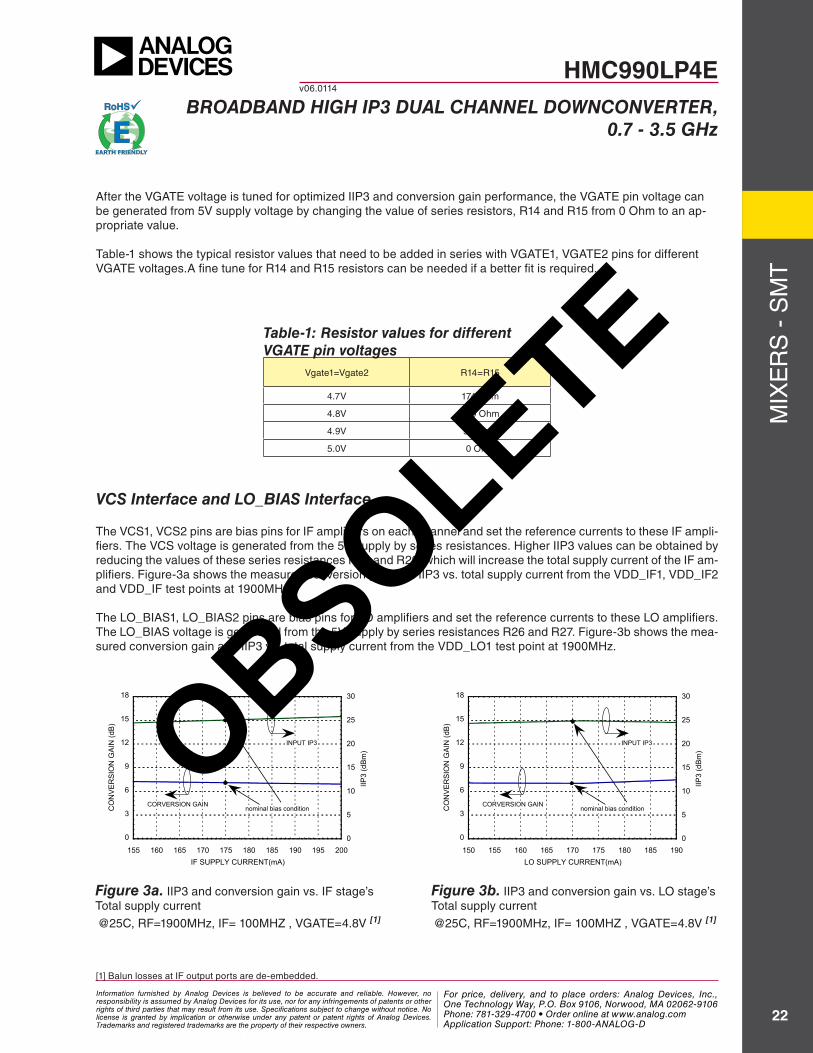
Table-1: Resistor values for different VGATE pin voltages
After the VGATE voltage is tuned for optimized IIP3 and conversion gain performance, the VGATE pin voltage can be generated from 5V supply voltage by changing the value of series resistors, R14 and R15 from 0 Ohm to an ap-propriate value.
Table-1 shows the typical resistor values that need to be added in series with VGATE1, VGATE2 pins for different VGATE voltages.A fine tune for R14 and R15 resistors can be needed if a better fit is required.
VCS Interface and LO_BIAS Interface
The VCS1, VCS2 pins are bias pins for IF amplifiers on each channel and set the reference currents to these IF ampli-fiers. The VCS voltage is generated from the 5V supply by series resistances. Higher IIP3 values can be obtained by reducing the values of these series resistances R28 and R29, which will increase the total supply current of the IF am-plifiers. Figure-3a shows the measured conversion gain and IIP3 vs. total supply current from the VDD_IF1, VDD_IF2 and VDD_IF test points at 1900MHz.
The LO_BIAS1, LO_BIAS2 pins are bias pins for LO amplifiers and set the reference currents to these LO amplifiers. The LO_BIAS voltage is generated from the 5V supply by series resistances R26 and R27. Figure-3b shows the mea-sured conversion gain and IIP3 vs. total supply current from the VDD_LO1 test point at 1900MHz.
0
3
6
9
12
15
18
155 160 165 170 175 180 185 190 195 2000
5
10
15
20
25
30
CO
NVE
RSI
ON
GAI
N (d
B)
IIP3
(dBm
)
IF SUPPLY CURRENT(mA)
INPUT IP3
CORVERSION GAINnominal bias condition
Figure 3a. IIP3 and conversion gain vs. IF stage’s Total supply current
@25C, RF=1900MHz, IF= 100MHZ , VGATE=4.8V [1]
0
3
6
9
12
15
18
150 155 160 165 170 175 180 185 1900
5
10
15
20
25
30
CO
NVE
RSI
ON
GAI
N (d
B)
IIP3
(dBm
)
LO SUPPLY CURRENT(mA)
INPUT IP3
CORVERSION GAINnominal bias condition
Figure 3b. IIP3 and conversion gain vs. LO stage’s Total supply current
@25C, RF=1900MHz, IF= 100MHZ , VGATE=4.8V [1]
[1] Balun losses at IF output ports are de-embedded.
Information furnished by Analog Devices is believed to be accurate and reliable. However, no responsibility is assumed by Analog Devices for its use, nor for any infringements of patents or other rights of third parties that may result from its use. Specifications subject to change without notice. No license is granted by implication or otherwise under any patent or patent rights of Analog Devices. Trademarks and registered trademarks are the property of their respective owners.
For price, delivery, and to place orders: Analog Devices, Inc., One Technology Way, P.O. Box 9106, Norwood, MA 02062-9106 Phone: 781-329-4700 • Order online at www.analog.com Application Support: Phone: 1-800-ANALOG-D
OBSOLETE

For price, delivery and to place orders: Hittite Microwave Corporation, 20 Alpha Road, Chelmsford, MA 01824Phone: 978-250-3343 Fax: 978-250-3373 Order On-line at www.hittite.com
Application Support: Phone: 978-250-3343 or [email protected]
MIX
ER
S -
SM
T
23
HMC990LP4EBROADBAND HIGH IP3 DUAL CHANNEL DOWNCONVERTER,
0.7 - 3.5 GHz
v06.0114
IF Amplifiers Total Supply Current R28=R29
155mA 820 Ohm
180mA 590 Ohm
200mA 390 Ohm
Table-2: Resistor values for total supply current of IF Amplifiers
Table-2 and Table-3 show the typical resistor values that are used in series with VCS1, VCS2 and LO_BIAS1, LO_BIAS2 pins for different total supply current values of IF and LO stages. A fine tune for these resistors can be needed if a better fit is required.
External RF Matching
The HMC990LP4E’s RF inputs are internally broadband matched to 50Ω. RF inputs can be externally matched for a specific RF frequency band of interest to further improve Input IP3 (IIP3). Matching RF inputs to a specific RF fre-quency band can be easily accomplished by adding a series inductor and a shunt capacitor. See Table-4 for values of the external matching components for corresponding RF frequency bands. Figure-4 shows the application circuit with the external components on RF input pins.
LO_BIAS2 and VGATE1, VGATE2 pin voltages can be optimized for a specific RF frequency band by changing the resistor values in series with these pins. Table-1 shows the resistor values (R14, R15) for corresponding VGATE pin voltage. Table-4 shows the resistor value (R26) for recommended LO_BIAS2 pin voltage.
Figure-5 shows the measured conversion gain and IIP3 for 900MHz,1900MHz and 2500MHz RF frequency bands.
Table-4: Components for Selected Frequency Bands
Tune Option Lmatch Cmatch1, Cmatch2 R26Recommended VGATE1,2
Voltages
900 MHz 6.8nH 2.7pF Open 150 Ohms 5.0V
1900 MHz 2.7nH 1pF Open 270 Ohms 4.8V
2500MHz 1nH Open 1pF 270 Ohms 4.8V
LO Amplifier Total Supply Current R26=R27
150mA 620Ohm
170mA 270 Ohm
190mA 0 Ohm
Table-3: Resistor values for total supply current of LO Amplifier
Information furnished by Analog Devices is believed to be accurate and reliable. However, no responsibility is assumed by Analog Devices for its use, nor for any infringements of patents or other rights of third parties that may result from its use. Specifications subject to change without notice. No license is granted by implication or otherwise under any patent or patent rights of Analog Devices. Trademarks and registered trademarks are the property of their respective owners.
For price, delivery, and to place orders: Analog Devices, Inc., One Technology Way, P.O. Box 9106, Norwood, MA 02062-9106 Phone: 781-329-4700 • Order online at www.analog.com Application Support: Phone: 1-800-ANALOG-D
OBSOLETE

For price, delivery and to place orders: Hittite Microwave Corporation, 2 Elizabeth Drive, Chelmsford, MA 01824Phone: 978-250-3343 Fax: 978-250-3373 Order On-line at www.hittite.com
Application Support: Phone: 978-250-3343 or [email protected]
MIX
ER
S -
SM
T
24
HMC990LP4EBROADBAND HIGH IP3 DUAL CHANNEL DOWNCONVERTER,
0.7 - 3.5 GHz
v06.0114
Figure-4. Application Circuit for Narrowband RF Input Matching
0
3
6
9
12
15
18
700 800 900 1000 1100
25C85C-40C
0
5
10
15
20
25
30
CO
NV
ER
SIO
N G
AIN
(dB
)
IIP
3 (
dB
m)
FREQUENCY (GHz)
INPUT IP3
CORVERSION GAIN
0
3
6
9
12
15
18
1700 1800 1900 2000 2100 2200
25C-40C85C
5
10
15
20
25
30
35
CO
NV
ER
SIO
N G
AIN
(dB
)
IIP
3 (
dB
m)
FREQUENCY (GHz)
CORVERSION GAIN
INPUT IP3
Figure-5a. IIP3 and Conversion Gain with matching for 900 MHz band
VGATE=5.0 V, IF=100 MHz [1]
Figure-5b. IIP3 and Conversion Gain with matching for 1900 MHz band
VGATE=4.8 V, IF=100 MHz [1]
[1] Balun losses at IF output ports are de-embedded.
Information furnished by Analog Devices is believed to be accurate and reliable. However, no responsibility is assumed by Analog Devices for its use, nor for any infringements of patents or other rights of third parties that may result from its use. Specifications subject to change without notice. No license is granted by implication or otherwise under any patent or patent rights of Analog Devices. Trademarks and registered trademarks are the property of their respective owners.
For price, delivery, and to place orders: Analog Devices, Inc., One Technology Way, P.O. Box 9106, Norwood, MA 02062-9106 Phone: 781-329-4700 • Order online at www.analog.com Application Support: Phone: 1-800-ANALOG-D
OBSOLETE

For price, delivery and to place orders: Hittite Microwave Corporation, 20 Alpha Road, Chelmsford, MA 01824Phone: 978-250-3343 Fax: 978-250-3373 Order On-line at www.hittite.com
Application Support: Phone: 978-250-3343 or [email protected]
MIX
ER
S -
SM
T
25
HMC990LP4EBROADBAND HIGH IP3 DUAL CHANNEL DOWNCONVERTER,
0.7 - 3.5 GHz
v06.0114
0
3
6
9
12
15
18
2300 2400 2500 2600 2700
5
10
15
20
25
30
35
25C-40C85C
CO
NV
ER
SIO
N G
AIN
(dB
)
IIP
3 (
dB
m)
FREQUENCY (GHz)
CORVERSION GAIN
INPUT IP3
15
17
19
21
23
25
27
29
31
1900MHz
-10 -8 -6 -4 -2 0
IIP
3(d
Bm
)
RF POWER (dBm)
It is recommended to use high side LO injection for RF frequencies below 1GHz for better IIP3. For instance, higher IIP3 can be obtained if LO input is driven with high side at RF=900 MHz. Please refer to Figure-6.
Figure-5c. IIP3 and Conversion Gain with matching for 2500 MHz bandVGATE=4.8 V, IF=100 MHz [1]
Input IP3 Dependence on RF Input Power
The HMC990LP4E accepts a wide range of RF input power. Figure-7 shows the IIP3 vs. RF input power for 1900 MHz RF and 150 MHz IF.
Figure-7. IIP3 vs. RF Input Power, RF=1900MHz, IF=150MHz, VGATE=4.8V
15
17
19
21
23
25
27
29
31
0.7 1.1 1.5 1.9 2.3 2.7 3.1 3.5
High Side LO
Low Side LO
IIP
3 (
dB
m)
FREQUENCY (GHz)
Figure-6. Input IP3 vs. High Side LO & Low Side LO @ VGATE=4.8V
[1] Balun losses at IF output ports are de-embedded.
Information furnished by Analog Devices is believed to be accurate and reliable. However, no responsibility is assumed by Analog Devices for its use, nor for any infringements of patents or other rights of third parties that may result from its use. Specifications subject to change without notice. No license is granted by implication or otherwise under any patent or patent rights of Analog Devices. Trademarks and registered trademarks are the property of their respective owners.
For price, delivery, and to place orders: Analog Devices, Inc., One Technology Way, P.O. Box 9106, Norwood, MA 02062-9106 Phone: 781-329-4700 • Order online at www.analog.com Application Support: Phone: 1-800-ANALOG-D
OBSOLETE

For price, delivery and to place orders: Hittite Microwave Corporation, 2 Elizabeth Drive, Chelmsford, MA 01824Phone: 978-250-3343 Fax: 978-250-3373 Order On-line at www.hittite.com
Application Support: Phone: 978-250-3343 or [email protected]
MIX
ER
S -
SM
T
26
HMC990LP4EBROADBAND HIGH IP3 DUAL CHANNEL DOWNCONVERTER,
0.7 - 3.5 GHz
v06.0114
0
2
4
6
8
10
12
0 100 200 300 400 500 600 700
CG
CO
NV
ER
SIO
N G
AIN
(dB
)
FREQUENCY (GHz)
Figure-8. Conversion gain vs. IF Frequency @ LO=1.5GHz [1]
IF Output Interface
The HMC990LP4E’s differential IF output pins are biased at the 5V supply voltage through choke inductors as shown in the application circuit. The default values of these choke inductors are 680nH. Figure-8 shows the measured con-version gain vs. IF frequency where 1-dB IF bandwidth is around 470MHz and 3-dB IF bandwidth is above 700MHz. Higher IF bandwidth values can be obtained by reducing the value of the choke inductors.
The baluns at the IF outputs are used to convert the 200 Ohms differential output impedance of HMC990LP4E to single-ended 50 Ohms for characterization.
[1] Balun losses at IF output ports are de-embedded.
Information furnished by Analog Devices is believed to be accurate and reliable. However, no responsibility is assumed by Analog Devices for its use, nor for any infringements of patents or other rights of third parties that may result from its use. Specifications subject to change without notice. No license is granted by implication or otherwise under any patent or patent rights of Analog Devices. Trademarks and registered trademarks are the property of their respective owners.
For price, delivery, and to place orders: Analog Devices, Inc., One Technology Way, P.O. Box 9106, Norwood, MA 02062-9106 Phone: 781-329-4700 • Order online at www.analog.com Application Support: Phone: 1-800-ANALOG-D
OBSOLETE