Embed Size (px)
Citation preview

"Tha
les
conf
ide n
tial.
All
right
s re
serv
ed"
Research & Technology
OBFN activities within Thales Photonic LabD. Dolfi, L. Morvan ,… Thales Research & Technology – FrJ. Chazelas, C. Fourdin, S. Formont,… Thales Système s AéroportésT. Merlet,… Thales Air SystemsM. Maignan, M. Sotom,… Thales Alenia Space
2
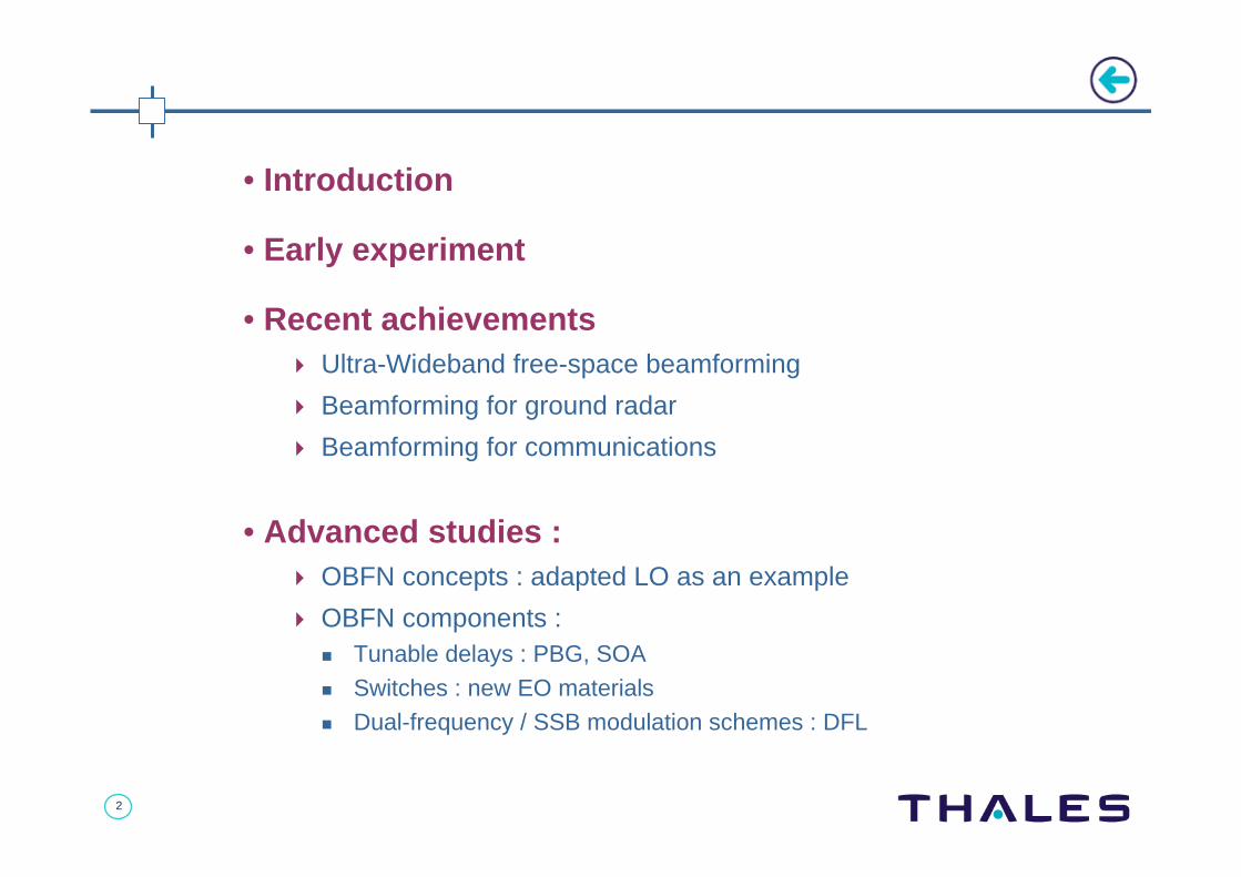
• Introduction
• Early experiment
• Recent achievements Ultra-Wideband free-space beamforming
Beamforming for ground radar
Beamforming for communications
• Advanced studies : OBFN concepts : adapted LO as an example
OBFN components : Tunable delays : PBG, SOA
Switches : new EO materials Dual-frequency / SSB modulation schemes : DFL

3
Thales Air Systems Div• RF & Digital optical linkdevelopments• Photonic architectures for ground based radars
Thales PhotonicsBGs-Corporate Lab.
Thales Photonics Lab.
Thales Research & Techno.•photonic architectures optoelectronic processing
Thales Netherlands naval applications
Thales Aerospace Div.• RF modules and optical links developments• Photonic architectures inairborne systems Research Institutes
• Wideband RF Summation• Switching matrices • Photo HBT & mixers• Dual frequencysources….
Thales Comm. Mil Com applications
SMEs • RF optical modules• Integrated WDM modules• Optical waveguides• …Alcatel-Thales 3-5 Lab.
optoelectroniccomponents
Thales AleniaSpace
satellite applications
TTCS•photonic architectures for PAA
Thales@NTU•photonic components
Thales Laser solid state lasers
Thales Sensors UKnaval ESM appli.

4
Optically controlled phased array antennas
Transmit mode

5
• Introduction
• Early experiment
• Recent achievements Ultra-Wideband free-space beamforming
Beamforming for ground radar
Beamforming for communications
• Advanced studies : OBFN concepts : adapted LO as an example
OBFN components : Tunable delays : PBG, SOA
Switches : new EO materials Dual-frequency / SSB modulation schemes : DFL

6
SLM i : polarization rotation
Free-space TTD
RF signal heterodyne generation
(delay/phase control)

7
Implementation of the phase control
Electrically controlled birefringent mode
p x p pixels
on channel k: i(k)=i0 cos(2π f t + 2π e ∆n(Vk)/λ) with ∆n(Vk)=n(Vk)-n0

8
Delays switching
N SLMs 2N delays
each SLMi : pxp pixels
channel k: ik(t)=i0 cos(2π f t + 2π f Σ εkj 2j-1 τ) If reflexion on PBSj εkj = 1
Else εkj = 0

9
Free-space optical TTD for S band antenna scanning
• delays: 5 bits
• phase control: 6 bits• 16 channels, 16 radiating elements• antenna beam pattern:
scan angle : ± 20° BW : 2700 - 3100 MHz no beam squint

10
• Introduction
• Early experiment
• Recent achievements Ultra-Wideband free-space beamforming
Beamforming for ground radar
Beamforming for communications
• Advanced studies : OBFN concepts : adapted LO as an example
OBFN components : Tunable delays : PBG, SOA
Switches : new EO materials Dual-frequency / SSB modulation schemes : DFL, SSB, FS

11
Compact True Time Delay module for transmit and receive modes
input fibresoutput fibres
BW = 2-20GHz 8 channels, 8 radiating elts unit delay τ=6.5ps 5 SLMs 32 delays/ch. ton=20ms, toff=100ms
20 cm
measured far field pattern for:
scan angle : ± 20° frequency : 6 – 18 GHz no beam squint

12
SLM (Spatial Light Modulator)
PBS (Polarization Beam Splitter)
Gratings
Holographic backplane concept
Integrated 2D True time delay implementation
for airborne applications
Advanced concept for ultra-compact architecture

13
• Introduction
• Early experiment
• Recent achievements Ultra-Wideband free-space beamforming
Beamforming for ground radar
Beamforming for communications
• Advanced studies : OBFN concepts : adapted LO as an example
OBFN components : Tunable delays : PBG, SOA Switches : new EO materials Dual-frequency / SSB modulation schemes : DFL
14
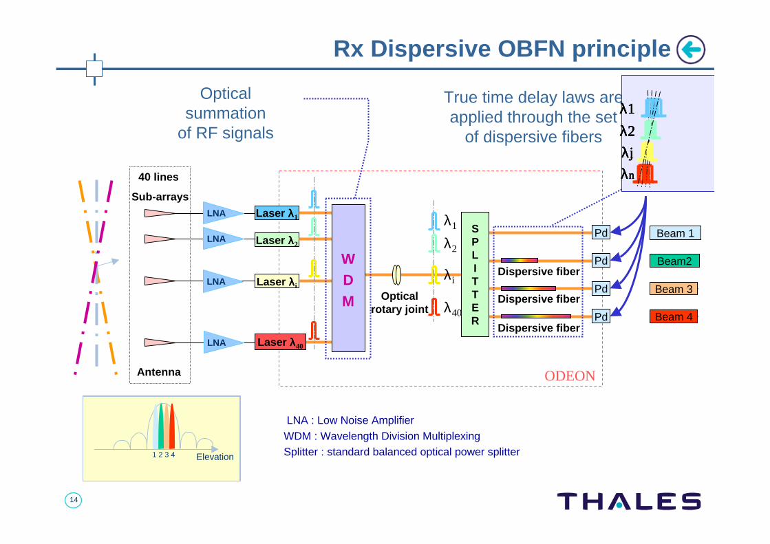
Dispersive fiber
Rx Dispersive OBFN principle
Laser λλλλ1
Laser λλλλ2
Laser λλλλi
Laser λλλλ40
40 lines
Sub-arrays
Opticalrotary joint
Beam 1
Beam 3
Beam 4
ODEONAntenna
Beam2WDM
LNA : Low Noise AmplifierWDM : Wavelength Division MultiplexingSplitter : standard balanced optical power splitter
LNA
LNA
LNA
LNA λ1
λ2
λi
λ40
Opticalsummation
of RF signals
Dispersive fiber
Dispersive fiber
True time delay laws are applied through the set
of dispersive fibers
Pd
Pd
Pd
Pd
SPLITTER
Elevation
λ1
λ2
λj
λn
1 Elevation
λ1
λ2
λj
λn
1 2 Elevation
λ1
λ2
λj
λn
1 2 3 Elevation
λ1
λ2
λi
λn
1 2 3 4 Elevation
15
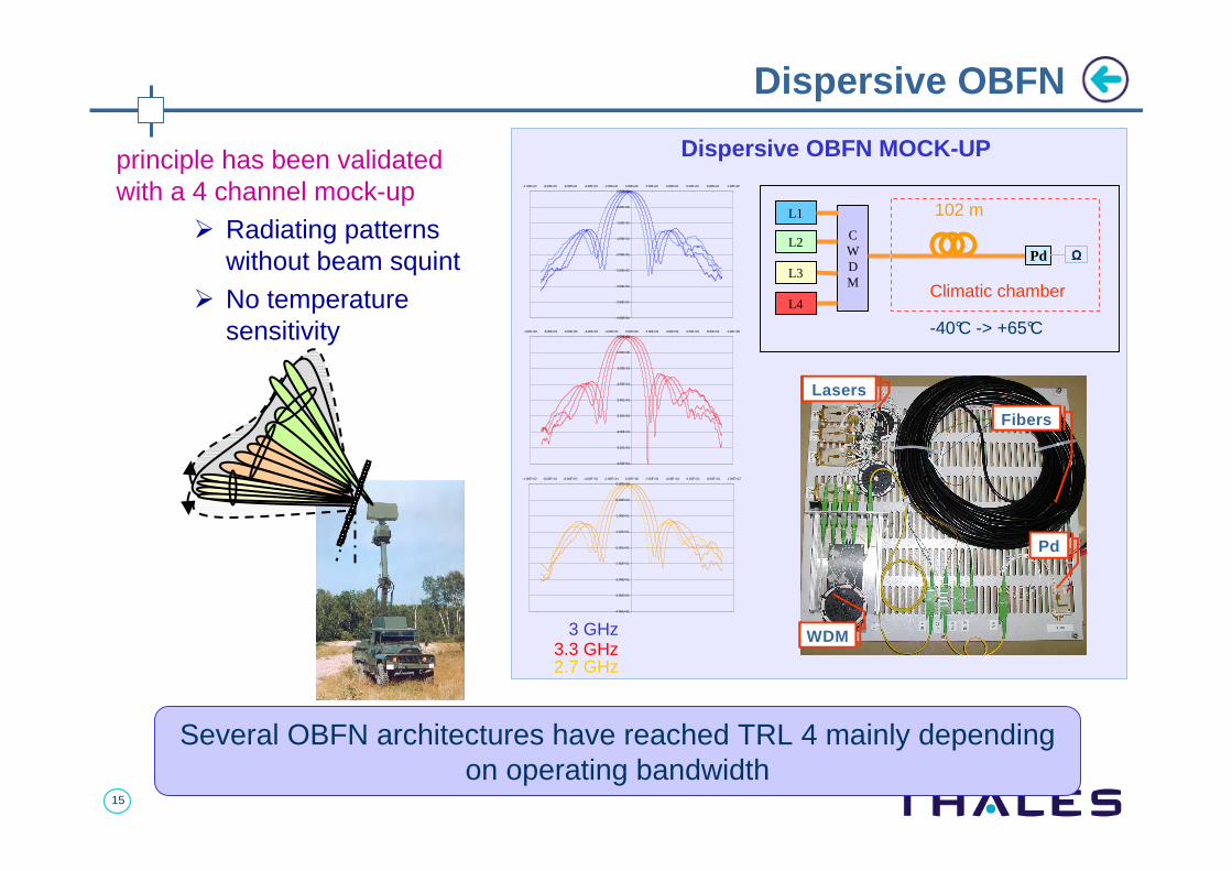
Dispersive OBFN
Several OBFN architectures have reached TRL 4 mainly dependingon operating bandwidth
Lasers
WDM
Fibers
Pd
Lasers
WDM
Fibers
Pd
ΩΩΩΩPd
102 mCWDM
L1
L2
L3
L4Climatic chamber
-40°C -> +65°C
3 GHz
2.7 GHz3.3 GHz
Dispersive OBFN MOCK-UP
-4.00E+01
-3.50E+01
-3.00E+01
-2.50E+01
-2.00E+01
-1.50E+01
-1.00E+01
-5.00E+00
0.00E+00
-1.00E+02 -8.00E+01 -6.00E+01 -4.00E+01 -2.00E+01 0.00E+00 2.00E+01 4.00E+01 6.00E+01 8.00E+01 1.00E+02
-4.00E+01
-3.50E+01
-3.00E+01
-2.50E+01
-2.00E+01
-1.50E+01
-1.00E+01
-5.00E+00
0.00E+00
-1.00E+02 -8.00E+01 -6.00E+01 -4.00E+01 -2.00E+01 0.00E+00 2.00E+01 4.00E+01 6.00E+01 8.00E+01 1.00E+02
-4.00E+01
-3.50E+01
-3.00E+01
-2.50E+01
-2.00E+01
-1.50E+01
-1.00E+01
-5.00E+00
0.00E+00
-1.00E+02 -8.00E+01 -6.00E+01 -4.00E+01 -2.00E+01 0.00E+00 2.00E+01 4.00E+01 6.00E+01 8.00E+01 1.00E+02
principle has been validatedwith a 4 channel mock-up
Radiating patterns without beam squint
No temperaturesensitivity

16
• Introduction
• Early experiment
• Recent achievements Ultra-Wideband free-space beamforming
Beamforming for ground radar
Beamforming for communications
• Advanced studies : OBFN concepts : adapted LO as an example
OBFN components : Tunable delays : PBG, SOA
Switches : new EO materials Dual-frequency / SSB modulation schemes : DFL

17
Outline
Within SATn’LIGHT :
Optically Controlled Antenna demonstrator
Building blocks overview
Dual-Frequency laser
Single-polarization Modulator
Phase & Amplitude Spatial Light Modulators
Optical summation module

18
Selected antenna concept
Within SAT ‘N LIGHT we have selected a FAFR (Focal Array Fed Reflector) Rx antenna as a “study case”.
• well-suited for narrow angular coverage for GEO satellite
• based on cheap radiating aperture of a reflector
• many clusters of horns form numerous beams
Ka band, 1 GHz bandwidth, diameter = 1.2 m, focal l ength = 1 m
170 feeds for 34 beams in Northern Hemisphere

19
Why to optically steer an active antenna ?
Beam forming is a complex architecture from 170 RF inputs towards 34 outputs with
≈≈≈≈ 400 RF amplitude controls
≈ 400 RF phase controls
≈ 200 splitters / combiners
Optical architectures lead to drastic weight and volume savings.
Among the 2 classes of optical architectures :
• True Time Delay Beam Steering
• “Coherent” Phase Steering
We have selected the latter approach since it corresponds to the ultimate integration capacity for satellite application
Coherent Optical Controlled Antenna (OCA) estimation* :•Mass < 50 kg•Consumption < 220 W•Volume < 6 liters
* From SAT N LIGHT phase 1

20
Heterodyne source
FAFR implementation of OCA architecture
detectordetector
detectordetector
modulator
signal RF 1
LO
Beam 1
Beam 34
Phase weight 34x12 Amplitude weights : 34x12
modulatormodulator
modulatormodulatormodulator
Wafer 1
Wafer 7signal RF 170
signal RF 145
signal RF 25
Optical fiber
Heterodyne source
Patent Fr 99 13358 (registration number) T. MERLET, O. MAAS « Dispositif de commande pour la formation de plusieurs faisceaux simultanés de réception radar à antenne à balayage électronique »Patent Fr 2 779 579 T. MERLET, O. MAAS, D. DOLFI « Dispositif de commande optique pour l’émission et la réceptiond’un radar large bande »

21
Optically-controlled antenna demo
• Optically Controlled Active antenna (OCA) is a proof of conceptdemonstrator based on a coherent optical architecture
• Heterodyne LO generation owing to cross-polarised modes in a solid-state cavity. New concept• RF Phase modulation on a single-polarisation New concept• Parallel 2D matrix for phase and amplitude weightings• Optical summation and optical Mixing on a single device New concept
• OCA demonstrator is composed of 4 building blocks
• Dual-Frequency Laser• Single-polarization optical modulator• Amplitude and phase weighting module• Optical Summation module

22
Dual Frequency laser
Single polarization optical modulator
Amplitude and phase weighting module
Optical summation
module
Optically-controlled antenna demo

23
Single Polarization Modulator
FC/APC FC/APCPolarisation
Maintaining Fiber
Polarisation
Maintaining Fiber
Coherent architectures are based upon delay coding in the range of 1 optical wavelength (1 µm).
• For RF phase stability, optical beams shall witness the same variations.
• Beams need to be carried on superposed on the same media
“Single polarization modulator” means :
• A modulator that transmit both polarizations, contrary to usual modulators.
• A modulator that only modulates one of the polarization.
Refer to Photline presentation for detailed explanations

24
Summation module : manufacturing
Box with:• integrated PIN detector• MW output (and DC bias)
XYZ positioner to adjust optical fibre position before
hermetic sealing
Fibre bunch
8 fibers gather in a bunch shines a single large surface photodetector
25
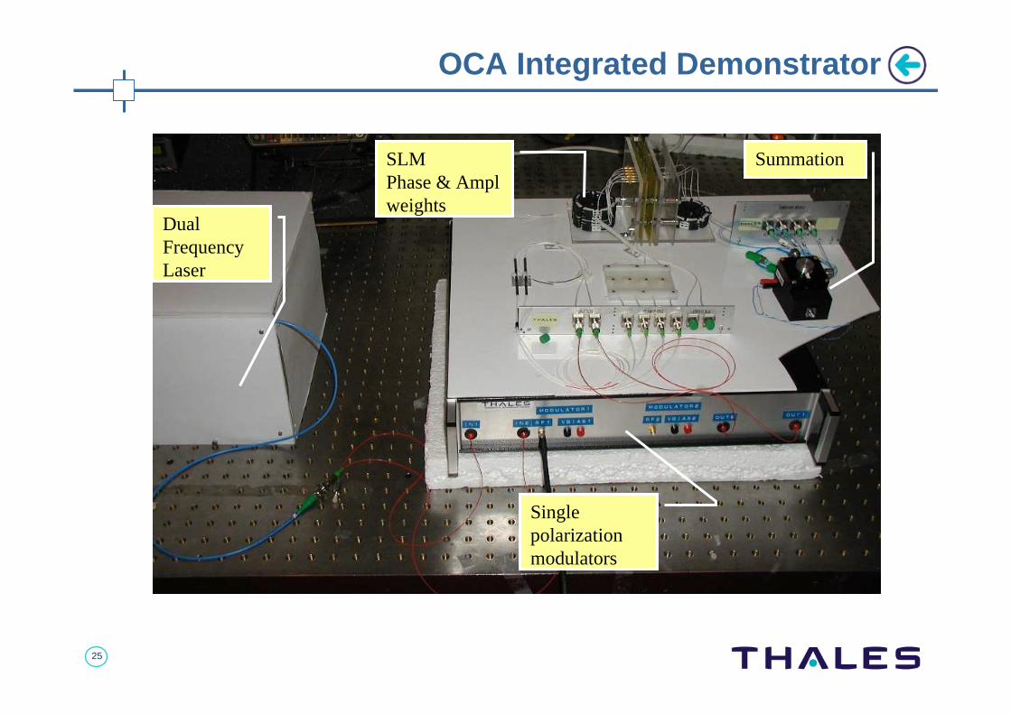
Dual Frequency Laser
SLMPhase & Ampl weights
Single polarization modulators
Summation
OCA Integrated Demonstrator

26
• Introduction
• Early experiment
• Recent achievements Ultra-Wideband free-space beamforming
Beamforming for ground radar
Beamforming for communications
• Advanced studies : OBFN concepts : adapted LO as an example
OBFN components : Tunable delays : PBG, SOA
Switches : new EO materials Dual-frequency / SSB modulation schemes : DFL (+SSB Mod, FS : Selex SI)

27
• microwave signals spread over a large dynamic range (u p to 100 dB)
• frequency bandwidth from <10% (radar, comm) up to 2- 18 GHz (E.W)
• in-phase addition over a large frequency BW of the rece ived signals with aprecision of few degrees
need of pxp analog microwave / optical links with large dynamic range and low noise figure
limited dynamic range of opto-links (typ. 90-95 dB in 1 MHz BW)
architecture with matched local oscillator (time-delayed and optically carried)
Analog processing of the receive mode

28
Time reversal vs matched L.O
τ τ τ τ j
transmitted
received
τ τ τ τ j
transmitted
received
matched LO
direct transposition time reversal matched L.O phase conjugation

29
Matched L.OImplementation of the delays
• optical carriers of the transmitted signal and of the L.O - with crossed polarizations - at different wavelengths
• complementary time delays on each channel i :- τmax-τi for the matched L.O- τi for the transmitted signal
SLM1 SLM2
ftflo

30
Matched L.O architecture
λ1
λ2
ftr
fLO
2:1 2D time delaynetwork
⊗fLO , τmax-τi
⊗
Radar Processing
ftr,τi
ftr
fr
fLO-fr
frPDi
PDn
T/R module
λ1
λ2
λ1 ,λ2
in phaseI.F signals

31
Matched Local Oscillator Architecturesingle mixing
on channel j :• transmitted signal : cos [ 2π ftr ( t - τ j ) ]
• local oscillator : cos [ 2π fLO ( t - (τ max - τ j ) ) ]
• received signal : cos [ 2π fr ( t - T + τ j ) ]
• intermediate frequency fI signal :
cos [ 2π ( fLO - fr ) t + 2π ( fLO - fr )τ j - 2π fLOτ max + 2π fr T ]
in-phase addition of the signals at f I when 2ππππ ( fLO - fr ) ττττ j << phasequantization
τ τ τ τ j
tr.
rec.
LO

32
Experimental results double mixing
I.F signal for time delay ττττ = 450ps between the channels
Two channel architecture with:• f = 2.8 GHz• I.F= 700 MHz
in phase I.F signalsresidual errors ∆τ < 10 ps, ∆φ ~ 5o
I.F signal for no delay between the
channels

33
Transmission and optical processing of RF signals
Need of variable delay lines for basic processing functions:• beam control of phased array antennas, programmable filtering
• spectral analysis of large BW microwave signals• radar phase conjugation
tuneablelaser
microwavemodulation
S(t)photodiode
S(t-τ)
- VECSEL in reflexion config.
« slow light » in a photonic crystal
membrane**
analog optoelectronic link
* D. Pastor et al., Electron. Lett., 34, 1684, 1998** S. Combrié et al., Electron. Lett., 42, 86, 2006*** J. Mørket al., Optics Express., 13, 20, 2005
the signal of interest is the microwave modulation itself, not the envelope
Semicond OpticalAmplifier
« slow light » in SOA*
- dispersive fibre (photonic crystal)

34
Photonic Crystal tunable delay preliminary demonstration
• device length: L = 1 mm
• measured phase shift: 30 deg@4GHz
• corresp. time delay: τ = 21 ps
4
5
6
7
8
9
10
11
grou
p in
dex
ng
1520 1540 1560 1580 1600 1620wavelength (nm)
waveguide dispersion
τ (λ)= ∆n (λ).L / c
∆n (λ) = 5 for ∆λ=30 nm
45
40
35
30
25
20
prop
agat
ion
dela
y
∆∆ ∆∆ ττ ττ,
ps
161516101605160015951590wavelength, nm
30
40
50
60
phase shift ϕϕ ϕϕ , deg
4
5
6
7
8
9
10
11
grou
p in
dex
ng
1520 1540 1560 1580 1600 1620
wavelength (nm)
waveguide dispersion
∆∆∆∆ττττ ≈≈≈≈ 20 ps
laser accordable modulateur RF
@ 4GHz
S(t)photodiode
S(t-τ)
struct. photoniquelaser accordable modulateur RF
@ 4GHz
S(t)
laser accordable modulateur RF
@ 4GHz
S(t)photodiode
S(t-τ)
photodiode
S(t-τ)
struct. photoniquetuneable
laserRF modulation
@ 4 GHz photonic crystalstructure

35
70 mA 300 mA
Co-propagative set-up
∆τ
300 mA
70 mA∆τ∆τ
300 mA
70 mA
Ω∆=∆
∆=∆
∫ dL
cn
L
cn
goptique
gg
τω
τ
0
5
10
15
20
25
0 2 4 6 8 10
Frequency (GHz)
phas
e (d
eg)
∆τ = ∆φ / ω
0
5
10
15
20
25
0 2 4 6 8 10
Frequency (GHz)
phas
e (d
eg)
0
5
10
15
20
25
0 2 4 6 8 10
Frequency (GHz)
phas
e (d
eg)
∆τ = ∆φ / ω
For a given fRF (typ. around 5 GHz) :ISOA
Vbias
Laser
fRF
Polarisationcontroller
Modulator(single side
band)SOA
Isolator
ω0ω0 ω0+2πfRF
Isolator
EDFA
Photo detector
pump
probeconjugate
pump
probe
ISOA
Vbias
Laser
fRF
Polarisationcontroller
Modulator(single side
band)SOA
Isolator
ω0ω0 ω0+2πfRF
Isolator
EDFA
Photo detector
ISOA
Vbias
Laser
fRF
Polarisationcontroller
Modulator(single side
band)SOA
Isolator
ω0ω0 ω0+2πfRF
Isolator
EDFA
Photo detector
ISOA
Vbias
Laser
fRF
Polarisationcontroller
Modulator(single side
band)SOA
Isolator
ω0ω0ω0 ω0+2πfRFω0 ω0+2πfRF
Isolator
EDFA
Photo detector
pump
probeconjugate
pump
probe
** from Selex S.I
Measurement of the time delays generated with a SOA

36
Measurement of the time delays generated with a SOA
modelisation+ measurements
@ 300mA, Pin = 0.8mW
Frequency (GHz)
Tim
e de
lay
(ps)
-50
-45
-40
-35
-30
-25
-20
-15
-10
-5
0
5
0 2 4 6 8 10 12 14 16
Frequency GHz
Tim
ede
lay
(ps)
Pin = 4 mW @ ISOA
=220mA
Measurements from VNA-50
-45
-40
-35
-30
-25
-20
-15
-10
-5
0
5
0 2 4 6 8 10 12 14 16
-50
-45
-40
-35
-30
-25
-20
-15
-10
-5
0
5
0 2 4 6 8 10 12 14 16
Frequency GHz
Tim
ede
lay
(ps)
Pin = 4 mW @ ISOA
=220mA
Measurements from VNA
0
0,5
1
1,5
2
2,5
0 2 4 6 8 10
Frequency (GHz)
delta
n (
x1E
-3)
∆n (x 10-3)
• Time delay from 4 to 45 ps
• Bandwidth : more than 10 GHz
• “Slowlight” with a factor from 2 to 20
• Index variation : few 10-3 (through L=750 µm)
*
*VNA: vectorial network analyzer

37
2-channel experimental demonstration
same time delay measured for the 1-channel
configuration and for the 2-channel config.*
ISOA
Laser 1549,5 nm
fRF Polarisation controlers
Modulator
Vbias
SOA
Isolator
ω0 ω0 ω0+2πfRF
Isolator
EDFAs
Laser1529 nm
Modulator
Vbiasω1 ω1 ω1+2πfRF
PM Coupler
photodetector
oscilloscope
filter
-60
-50
-40
-30
-20
-10
00 5 10 15 20
Frequency (GHz)
mea
sure
d tim
e de
lay
(ps)
1-channel
2-channel
*for one channel present in the opto-link (Pin = 2mW) or
for two channels (Pin = 1mW for each)
38
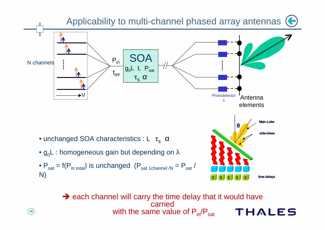
Applicability to multi-channel phased array antennas
• unchanged SOA characteristics : L τs α
• g0L : homogeneous gain but depending on λ
• Psat = f(Pin total) is unchanged (Psat 1channel /N = Psat / N)
each channel will carry the time delay that it would have carried
with the same value of Pin/Psat
SOAg0L L Psat
τs α
ν Photodetectors Antenna
elements
Pin
fRF
N channels
Main Lobe
side-lobes
ττττ ττττ ττττ ττττ ττττ time delays
θθθθMain Lobe
side-lobes
ττττ ττττ ττττ ττττ ττττ time delays
θθθθ
40
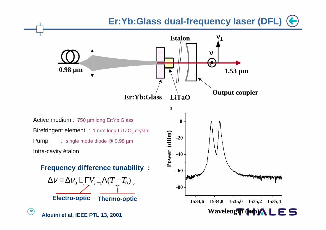
Er:Yb:Glass dual-frequency laser (DFL)
Active medium : 750 µm long Er:Yb:Glass
Birefringent element : 1 mm long LiTaO3 crystal
Pump : single mode diode @ 0.98 µm
Intra-cavity étalon
Output couplerEr:Yb:Glass LiTaO
3
0.98 µm 1.53 µm
Etalon νννν1111
νννν2222
)( 00 TTV −Λ+Γ+∆=∆ νν
Electro-optic Thermo-optic
Frequency difference tunability :
Alouini et al, IEEE PTL 13, 2001
1534,6 1534,8 1535,0 1535,2 1535,4
-80
-60
-40
-20
0
Pow
er(d
Bm
)
Wavelength (nm)

41
Er:Yb:Glass two-frequency laser (DFL)
Phase noise of the free-running beatnote
@ 2 GHz
Require stabilization for radar applications
40
20
0
-20
-40
-60
-80
-100
-120
101 102 103 104 105 106
phas
e-no
ise
PS
D (
dBra
d2 /H
z)
Frequency (Hz)107
40
20
0
-20
-40
-60
-80
-100
-120
101 102 103 104 105 106
phas
e-no
ise
PS
D (
dBra
d2 /H
z)
Frequency (Hz)107
~1 kHz linewidth
42
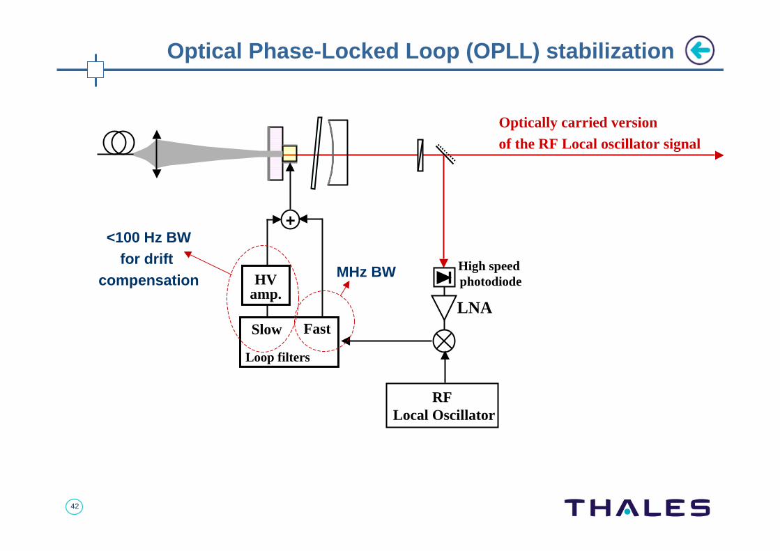
Optical Phase-Locked Loop (OPLL) stabilization
RFLocal Oscillator
Loop filters
FastSlow
High speedphotodiodeHV
amp.
+
LNA
<100 Hz BWfor drift
compensation MHz BW
Optically carried version
of the RF Local oscillator signal

43
DFL stabilization with an Optical Phase -Locked -Loop (OPLL)
40
20
0
-20
-40
-60
-80
-100
-120
101 102 103 104 105 106
phas
e-no
ise
PS
D (
dBra
d2 /H
z)
Frequency (Hz)
107
RF reference noise
Phase noise of the stabilized beatnote
Free-runningnoise

44
Fiber delay stabilization
Loop filters
FastSlow
HVamp.
+
ττττ1111
Stabilized output
Stabilization combining two delays
ττττ2222
Electro-optical
frequency
Discriminator
(EOFD)
νννν1111νννν2222
νν νν 11 11νν νν 22 22

45
Fiber delay stabilization
Phase noise of the stabilized beatnote : 1000 + 100 meters long fibers
both low and high frequency phase noise are reduced, detection + electronic noises are still limiting
40
20
0
-20
-40
-60
-80
-100
-120
101 102 103 104 105 106
phas
e-no
ise
PS
D (
dBra
d2 /H
z)
Frequency (Hz)107
2 to 6 GHz40
20
0
-20
-40
-60
-80
-100
-120
101 102 103 104 105 106
phas
e-no
ise
PS
D (
dBra
d2 /H
z)
Frequency (Hz)107
2 to 6 GHz
Theoretical limit is fixed by the shot noise level at
detection and the amount of delay :
Low noise, widely tunable, high frequency
oscillators for radar applications
ττπϕ /1,
2222
<<= ffI
eS
phot
-150 dBrad²/Hz @10 kHz( 1 km long fiber and 10 mA photocurrent Iphot)

46
• Optical technology offers : Potential for reducing mass and volume (e.g. the good performance of
optical fiber as transmission medium regarding weight, volume and loss can implement compact optically-based TTD beamfoming structures).
Antenna remoting
Advance functionality (processing of different types of signals,wideband, multibeam, reconfigurable)
Different approaches to optical beamforming that can be combined to perform the most suitable optical architecture regarding the application targeted
• New approaches for time delay implementation under studies will offer in the future a higher level of integration
Conclusion