Embed Size (px)
Citation preview
Document Number: CD1020 Rev. 2.0, 2/2018
NXP Semiconductors Advance Information
MULTIPLE SWITCH DETECTION INTERFACE
CD1020
Applications• Automotive
• Heating ventilation and air conditioning (HVAC) • Lighting• Central gateway/in-vehicle networking• Gasoline engine management
ES SUFFIX (PB-FREE)98ASA00656D
32-PIN QFN (WF-TYPE)
22 channel multiple switch detection interfaceThe CD1020 is a cost optimized switch detection interface device (MSDI) designed to detect the closing and opening of up to 22 switch contacts. The switch status, either open or closed, is transferred to the microprocessor unit (MCU) through a Serial Peripheral Interface (SPI). This SMARTMOS device also features a 22-to-1 analog multiplexer for reading the input channels as analog inputs. The analog selected input signal is buffered and provided on the AMUX output pin for the MCU to read.The CD1020 device has two modes of operation, normal and low-power mode (LPM). Normal mode allows programming of the device and supplies switch contacts with pull-up or pull-down current as it monitors the change of state on the switches. The LPM provides low quiescent current, which makes the CD1020 ideal for automotive and industrial products requiring low sleep-state currents.The low cost MSDI is available in high power, space saving wettable flank 5x5 mm QFN package.Features• Fully functional operation 6.0 V ≤ VBATP ≤ 36 V• Full parametric operation 6.0 V ≤ VBATP ≤ 28 V • Operating switch input voltage range from –1.0 V to 36 V• Eight programmable inputs (switches to battery or ground) • 14 switch-to-ground inputs• Selectable wetting current (2, 8,12,16 mA)• Interfaces directly to an MCU using 3.3 V / 5.0 V SPI protocol• Selectable wake-up on change of state• Typical standby current IBATP = 30 A and IDDQ = 10 A• Active interrupt (INT_B) on change-of-switch state
Figure 1. CD1020 simplified application diagram
This document contains certain information on a product under development. NXP reserves the right to change or discontinue this product without notice.
© NXP B.V. 2018.
Table of Contents
1 Orderable parts . . . . . . . . . . . . . . . . . . . . . . . . . . . . . . . . . . . . . . . . . . . . . . . . . . . . . . . . . . . . . . . . . . . . . . . . . . . . . . . . . . . . . . . . 32 Internal block diagram . . . . . . . . . . . . . . . . . . . . . . . . . . . . . . . . . . . . . . . . . . . . . . . . . . . . . . . . . . . . . . . . . . . . . . . . . . . . . . . . . . . 43 Pin connections . . . . . . . . . . . . . . . . . . . . . . . . . . . . . . . . . . . . . . . . . . . . . . . . . . . . . . . . . . . . . . . . . . . . . . . . . . . . . . . . . . . . . . . . 5
3.1 Pinout . . . . . . . . . . . . . . . . . . . . . . . . . . . . . . . . . . . . . . . . . . . . . . . . . . . . . . . . . . . . . . . . . . . . . . . . . . . . . . . . . . . . . . . . . . . 53.2 Pin definitions . . . . . . . . . . . . . . . . . . . . . . . . . . . . . . . . . . . . . . . . . . . . . . . . . . . . . . . . . . . . . . . . . . . . . . . . . . . . . . . . . . . . . 5
4 General product characteristics . . . . . . . . . . . . . . . . . . . . . . . . . . . . . . . . . . . . . . . . . . . . . . . . . . . . . . . . . . . . . . . . . . . . . . . . . . . . 74.1 Maximum ratings . . . . . . . . . . . . . . . . . . . . . . . . . . . . . . . . . . . . . . . . . . . . . . . . . . . . . . . . . . . . . . . . . . . . . . . . . . . . . . . . . . . 74.2 Thermal characteristics . . . . . . . . . . . . . . . . . . . . . . . . . . . . . . . . . . . . . . . . . . . . . . . . . . . . . . . . . . . . . . . . . . . . . . . . . . . . . . 84.3 Operating conditions . . . . . . . . . . . . . . . . . . . . . . . . . . . . . . . . . . . . . . . . . . . . . . . . . . . . . . . . . . . . . . . . . . . . . . . . . . . . . . . . 94.4 Electrical characteristics . . . . . . . . . . . . . . . . . . . . . . . . . . . . . . . . . . . . . . . . . . . . . . . . . . . . . . . . . . . . . . . . . . . . . . . . . . . . . 9
5 General description . . . . . . . . . . . . . . . . . . . . . . . . . . . . . . . . . . . . . . . . . . . . . . . . . . . . . . . . . . . . . . . . . . . . . . . . . . . . . . . . . . . . 155.1 Features . . . . . . . . . . . . . . . . . . . . . . . . . . . . . . . . . . . . . . . . . . . . . . . . . . . . . . . . . . . . . . . . . . . . . . . . . . . . . . . . . . . . . . . . 155.2 Functional block diagram . . . . . . . . . . . . . . . . . . . . . . . . . . . . . . . . . . . . . . . . . . . . . . . . . . . . . . . . . . . . . . . . . . . . . . . . . . . 16
6 General IC functional description . . . . . . . . . . . . . . . . . . . . . . . . . . . . . . . . . . . . . . . . . . . . . . . . . . . . . . . . . . . . . . . . . . . . . . . . . . 176.1 Battery voltage ranges . . . . . . . . . . . . . . . . . . . . . . . . . . . . . . . . . . . . . . . . . . . . . . . . . . . . . . . . . . . . . . . . . . . . . . . . . . . . . 176.2 Power sequencing conditions . . . . . . . . . . . . . . . . . . . . . . . . . . . . . . . . . . . . . . . . . . . . . . . . . . . . . . . . . . . . . . . . . . . . . . . . 18
7 Functional block description . . . . . . . . . . . . . . . . . . . . . . . . . . . . . . . . . . . . . . . . . . . . . . . . . . . . . . . . . . . . . . . . . . . . . . . . . . . . . . 197.1 State diagram . . . . . . . . . . . . . . . . . . . . . . . . . . . . . . . . . . . . . . . . . . . . . . . . . . . . . . . . . . . . . . . . . . . . . . . . . . . . . . . . . . . . 197.2 Low-power mode operation . . . . . . . . . . . . . . . . . . . . . . . . . . . . . . . . . . . . . . . . . . . . . . . . . . . . . . . . . . . . . . . . . . . . . . . . . . 207.3 Input functional block . . . . . . . . . . . . . . . . . . . . . . . . . . . . . . . . . . . . . . . . . . . . . . . . . . . . . . . . . . . . . . . . . . . . . . . . . . . . . . 227.4 Oscillator and timer control functional block . . . . . . . . . . . . . . . . . . . . . . . . . . . . . . . . . . . . . . . . . . . . . . . . . . . . . . . . . . . . . 247.5 Temperature monitor and control functional block . . . . . . . . . . . . . . . . . . . . . . . . . . . . . . . . . . . . . . . . . . . . . . . . . . . . . . . . 257.6 WAKE_B control functional block . . . . . . . . . . . . . . . . . . . . . . . . . . . . . . . . . . . . . . . . . . . . . . . . . . . . . . . . . . . . . . . . . . . . . 257.7 INT_B functional block . . . . . . . . . . . . . . . . . . . . . . . . . . . . . . . . . . . . . . . . . . . . . . . . . . . . . . . . . . . . . . . . . . . . . . . . . . . . . 257.8 AMUX functional block . . . . . . . . . . . . . . . . . . . . . . . . . . . . . . . . . . . . . . . . . . . . . . . . . . . . . . . . . . . . . . . . . . . . . . . . . . . . . 257.9 Serial peripheral interface (SPI) . . . . . . . . . . . . . . . . . . . . . . . . . . . . . . . . . . . . . . . . . . . . . . . . . . . . . . . . . . . . . . . . . . . . . . 267.10 SPI control register definition . . . . . . . . . . . . . . . . . . . . . . . . . . . . . . . . . . . . . . . . . . . . . . . . . . . . . . . . . . . . . . . . . . . . . . . . 29
8 Typical applications . . . . . . . . . . . . . . . . . . . . . . . . . . . . . . . . . . . . . . . . . . . . . . . . . . . . . . . . . . . . . . . . . . . . . . . . . . . . . . . . . . . . 498.1 Application diagram . . . . . . . . . . . . . . . . . . . . . . . . . . . . . . . . . . . . . . . . . . . . . . . . . . . . . . . . . . . . . . . . . . . . . . . . . . . . . . . . 498.2 Bill of materials . . . . . . . . . . . . . . . . . . . . . . . . . . . . . . . . . . . . . . . . . . . . . . . . . . . . . . . . . . . . . . . . . . . . . . . . . . . . . . . . . . . 498.3 Abnormal operation . . . . . . . . . . . . . . . . . . . . . . . . . . . . . . . . . . . . . . . . . . . . . . . . . . . . . . . . . . . . . . . . . . . . . . . . . . . . . . . . 50
9 Packaging . . . . . . . . . . . . . . . . . . . . . . . . . . . . . . . . . . . . . . . . . . . . . . . . . . . . . . . . . . . . . . . . . . . . . . . . . . . . . . . . . . . . . . . . . . . 519.1 Package mechanical dimensions . . . . . . . . . . . . . . . . . . . . . . . . . . . . . . . . . . . . . . . . . . . . . . . . . . . . . . . . . . . . . . . . . . . . . 51
10 Reference section . . . . . . . . . . . . . . . . . . . . . . . . . . . . . . . . . . . . . . . . . . . . . . . . . . . . . . . . . . . . . . . . . . . . . . . . . . . . . . . . . . . . . 5511 Revision history . . . . . . . . . . . . . . . . . . . . . . . . . . . . . . . . . . . . . . . . . . . . . . . . . . . . . . . . . . . . . . . . . . . . . . . . . . . . . . . . . . . . . . . 55
NXP Semiconductors 2
CD1020
1 Orderable parts
This section describes the part numbers available to be purchased along with their differences.
Table 1. Orderable part variations
Part number Temperature (TA) Package Notes
–40 °C to 125 °C 32-pin QFN (WF-type) (1)
1. To order parts in tape and reel, add the R2 suffix to the part number.
MC33CD1020AES
Notes
3 NXP Semiconductors
CD1020
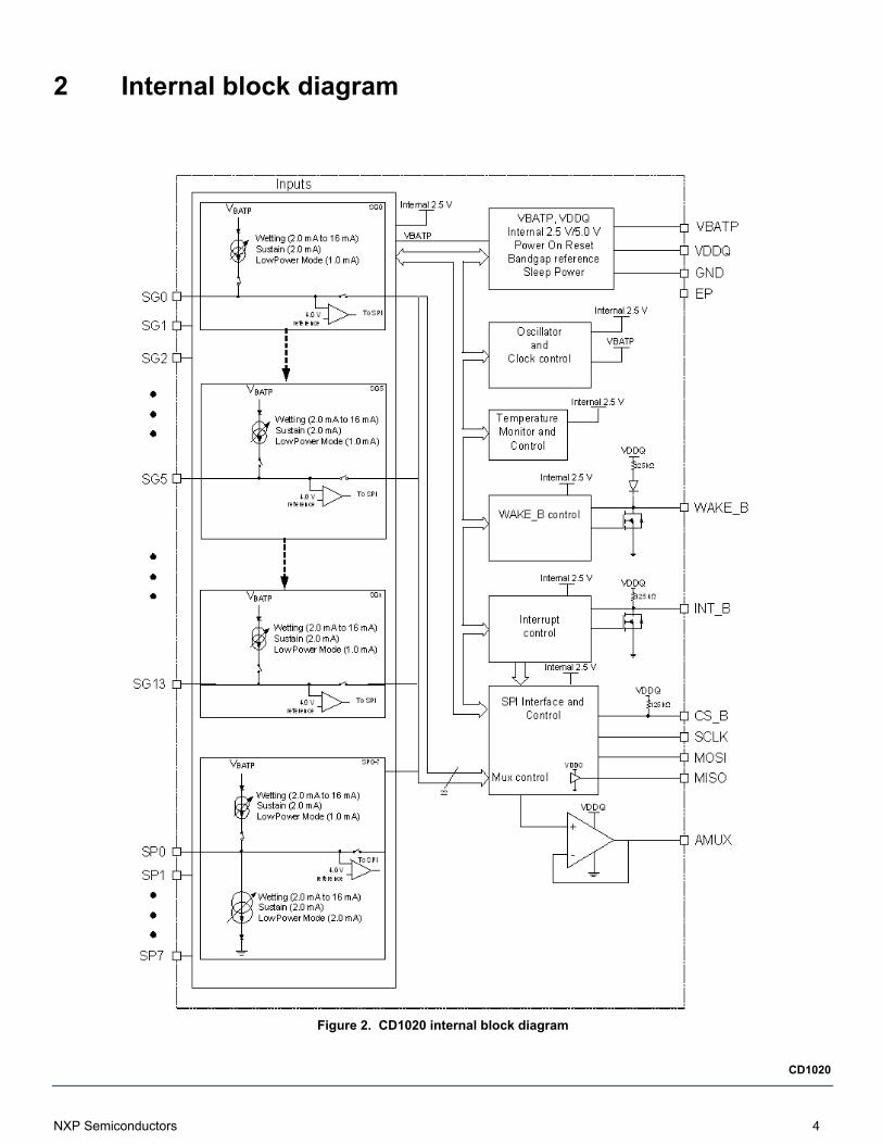
2 Internal block diagram
Figure 2. CD1020 internal block diagram
NXP Semiconductors 4
CD1020
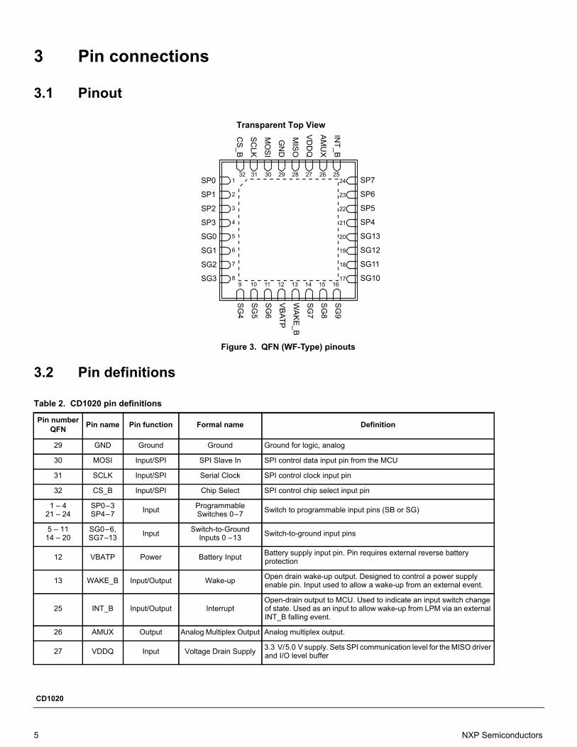
3 Pin connections
3.1 Pinout
Transparent Top View
1
2
3
4
5
6
7
89 10 11 12 13 14 15 16
32 31 30 29 28 27 26 2524
23
22
21
20
19
18
17
SP0
SP1
SP2
SP3
SG0
SG1
SG2
SG3
SG4
SG5
SG6
VBATP
WAKE_B
SG7
SG8
SG9
SP7
SP6
SP5
SP4
SG13
SG12
SG11
SG10
CS_B
SCLK
MO
SI
GN
D
MISO
VDD
Q
AMU
X
INT_B
Figure 3. QFN (WF-Type) pinouts
3.2 Pin definitions Table 2. CD1020 pin definitions
Pin numberQFN Pin name Pin function Formal name Definition
29 GND Ground Ground Ground for logic, analog
30 MOSI Input/SPI SPI Slave In SPI control data input pin from the MCU
31 SCLK Input/SPI Serial Clock SPI control clock input pin
32 CS_B Input/SPI Chip Select SPI control chip select input pin
1 – 421 – 24
SP0 – 3SP4 – 7 Input Programmable
Switches 0 – 7 Switch to programmable input pins (SB or SG)
5 – 1114 – 20
SG0 – 6,SG7 –13 Input Switch-to-Ground
Inputs 0 – 13 Switch-to-ground input pins
12 VBATP Power Battery Input Battery supply input pin. Pin requires external reverse battery protection
13 WAKE_B Input/Output Wake-up Open drain wake-up output. Designed to control a power supply enable pin. Input used to allow a wake-up from an external event.
25 INT_B Input/Output InterruptOpen-drain output to MCU. Used to indicate an input switch change of state. Used as an input to allow wake-up from LPM via an external INT_B falling event.
26 AMUX Output Analog Multiplex Output Analog multiplex output.
27 VDDQ Input Voltage Drain Supply 3.3 V/ 5.0 V supply. Sets SPI communication level for the MISO driver and I/O level buffer
5 NXP Semiconductors
CD1020
28 MISO Output/SPI SPI Slave Out Provides digital data from the CD1020 to the MCU.
EP Ground Exposed Pad It is recommended that the exposed pad is terminated to GND (pin 1) and system ground.
Table 2. CD1020 pin definitions (continued)
Pin numberQFN Pin name Pin function Formal name Definition
NXP Semiconductors 6
CD1020
4 General product characteristics
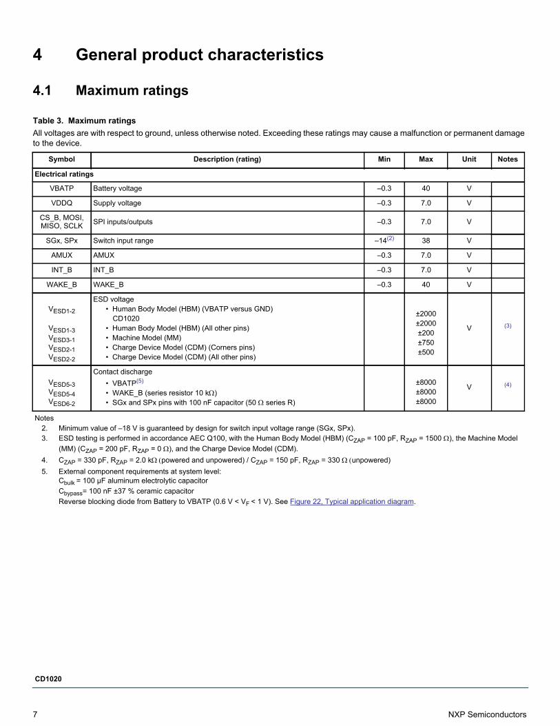
4.1 Maximum ratings
Table 3. Maximum ratings All voltages are with respect to ground, unless otherwise noted. Exceeding these ratings may cause a malfunction or permanent damage to the device.
Symbol Description (rating) Min Max Unit Notes
Electrical ratings
• Human Body Model (HBM) (VBATP versus GND)
• Human Body Model (HBM) (All other pins)• Machine Model (MM)• Charge Device Model (CDM) (Corners pins)• Charge Device Model (CDM) (All other pins)
• VBATP(5) • WAKE_B (series resistor 10 k) • SGx and SPx pins with 100 nF capacitor (50 series R)
Notes2. Minimum value of –18 V is guaranteed by design for switch input voltage range (SGx, SPx).3. ESD testing is performed in accordance AEC Q100, with the Human Body Model (HBM) (CZAP = 100 pF, RZAP = 1500 ), the Machine Model
(MM) (CZAP = 200 pF, RZAP = 0 ), and the Charge Device Model (CDM).4. CZAP = 330 pF, RZAP = 2.0 kpowered and unpowered) / CZAP = 150 pF, RZAP = 330 unpowered)5. External component requirements at system level:
Cbulk = 100 μF aluminum electrolytic capacitor Cbypass= 100 nF ±37 % ceramic capacitor Reverse blocking diode from Battery to VBATP (0.6 V < VF < 1 V). See Figure 22, Typical application diagram.
VBATP Battery voltage –0.3 40 V
VDDQ Supply voltage –0.3 7.0 V
CS_B, MOSI, MISO, SCLK SPI inputs/outputs –0.3 7.0 V
SGx, SPx Switch input range –14(2) 38 V
AMUX AMUX –0.3 7.0 V
INT_B INT_B –0.3 7.0 V
WAKE_B WAKE_B –0.3 40 V
VESD1-2
VESD1-3VESD3-1VESD2-1VESD2-2
ESD voltage
CD1020 ±2000±2000±200±750±500
V (3)
VESD5-3VESD5-4VESD6-2
Contact discharge ±8000 ±8000±8000
V (4)
7 NXP Semiconductors
CD1020
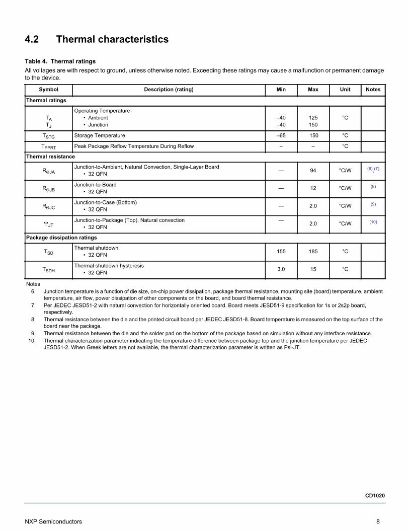
4.2 Thermal characteristics
Table 4. Thermal ratings All voltages are with respect to ground, unless otherwise noted. Exceeding these ratings may cause a malfunction or permanent damage to the device.
Symbol Description (rating) Min Max Unit Notes
Thermal ratings
• Ambient• Junction
Thermal resistance
• 32 QFN
• 32 QFN
• 32 QFN
• 32 QFN
Package dissipation ratings
• 32 QFN
• 32 QFN
6. Junction temperature is a function of die size, on-chip power dissipation, package thermal resistance, mounting site (board) temperature, ambient temperature, air flow, power dissipation of other components on the board, and board thermal resistance.
7. Per JEDEC JESD51-2 with natural convection for horizontally oriented board. Board meets JESD51-9 specification for 1s or 2s2p board, respectively.
8. Thermal resistance between the die and the printed circuit board per JEDEC JESD51-8. Board temperature is measured on the top surface of the board near the package.
9. Thermal resistance between the die and the solder pad on the bottom of the package based on simulation without any interface resistance.10. Thermal characterization parameter indicating the temperature difference between package top and the junction temperature per JEDEC
JESD51-2. When Greek letters are not available, the thermal characterization parameter is written as Psi-JT.
TATJ
Operating Temperature–40–40
125150
°C
TSTG Storage Temperature –65 150 °C
TPPRT Peak Package Reflow Temperature During Reflow – – °C
RJAJunction-to-Ambient, Natural Convection, Single-Layer Board — 94 °C/W (6),(7)
RJBJunction-to-Board — 12 °C/W (8)
RJCJunction-to-Case (Bottom) — 2.0 °C/W (9)
JTJunction-to-Package (Top), Natural convection — 2.0 °C/W (10)
TSDThermal shutdown 155 185 °C
TSDHThermal shutdown hysteresis 3.0 15 °C
Notes
NXP Semiconductors 8
CD1020
4.3 Operating conditionsThis section describes the operating conditions of the device. Conditions apply to the following data, unless otherwise noted.
Table 5. Operating conditionsAll voltages are with respect to ground, unless otherwise noted. Exceeding these ratings may cause a malfunction or permanent damage to the device.
Symbol Ratings Min Max Unit Notes
4.4 Electrical characteristics
4.4.1 Static electrical characteristics
VBATP Battery voltage 6.0 36 V
VDDQ Supply voltage 3.0 5.25 V
CS_B, MOSI, MISO, SCLK SPI inputs / outputs 3.0 5.25 V
SGx, SPx Switch input range –1.0 36 V
AMUX, INT_B AMUX, INT_B 0.0 5.25 V
WAKE_B WAKE_B 0.0 36 V
Table 6. Static electrical characteristics TA = –40 °C to +125 °C, VDDQ = 3.1 V to 5.25 V, VBATP = 6.0 V to 28.0 V, unless otherwise noted.
Symbol Characteristic Min Typ Max Units Notes
Power input
VBATP(POR)VBATP supply voltage POR
• VBATP supply Power-On-Reset voltage. 2.7 3.3 3.8 V
VBATPUV VBATP undervoltage rising threshold — 4.3 4.5 V
VBATPUVHYS VBATP undervoltage hysteresis 250 — 500 mV
VBATPOV VBATP overvoltage rising threshold 32 — 37 V
VBATPOVHYS VBATP overvoltage hysteresis 1.5 — 3.0 V
IBAT(ON)VBATP supply current
• All switches open, normal mode, tri-state disabled (all channels) — 7.0 12 mA
IBATP,IQ,LPM,P
VBATP low-power mode supply current (polling disabled)• Parametric VBATP, 6.0 V < VBATP < 28 V — — 40 μA
IPOLLING,IQVBATP polling current
• Polling 64 ms, 11 inputs of wake enabled — — 20 μA (11)
IVDDQ,NORMAL
Normal mode (IVDDQ)• SCLK, MOSI, WakeB = 0 V, CS_B, INT_B =VDDQ, no SPI communication, AMUX selected no input
— — 500 μA
IVDDQ,LPM
Logic low-power mode supply current• SCLK, MOSI = 0 V, CS_B, INT_B, WAKE_B = VDDQ, no SPI communication
— — 10 μA
VGNDOFFSETGround Offset
• Ground offset of Global pins to IC ground –1.0 — 1.0 V (20)
VDDQUV VDDQ undervoltage falling threshold 2.2 — 2.8 V
VDDQUVHYS VDDQ undervoltage hysteresis 150 — 350 mV
Switch input
9 NXP Semiconductors
CD1020
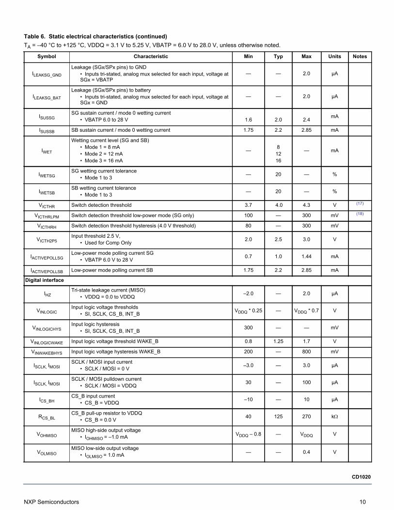
ILEAKSG_GND
Leakage (SGx/SPx pins) to GND• Inputs tri-stated, analog mux selected for each input, voltage at SGx = VBATP
— — 2.0 μA
ILEAKSG_BAT
Leakage (SGx/SPx pins) to battery• Inputs tri-stated, analog mux selected for each input, voltage at SGx = GND
— — 2.0 μA
ISUSSGSG sustain current / mode 0 wetting current
• VBATP 6.0 to 28 V 1.6 2.0 2.4 mA
ISUSSB SB sustain current / mode 0 wetting current 1.75 2.2 2.85 mA
IWET
Wetting current level (SG and SB)• Mode 1 = 8 mA• Mode 2 = 12 mA• Mode 3 = 16 mA
— 81216
— mA
IWETSGSG wetting current tolerance
• Mode 1 to 3 — 20 — %
IWETSBSB wetting current tolerance
• Mode 1 to 3 — 20 — %
VICTHR Switch detection threshold 3.7 4.0 4.3 V (17)
VICTHRLPM Switch detection threshold low-power mode (SG only) 100 — 300 mV (18)
VICTHRH Switch detection threshold hysteresis (4.0 V threshold) 80 — 300 mV
VICTH2P5Input threshold 2.5 V,
• Used for Comp Only 2.0 2.5 3.0 V
IACTIVEPOLLSGLow-power mode polling current SG
• VBATP 6.0 V to 28 V 0.7 1.0 1.44 mA
IACTIVEPOLLSB Low-power mode polling current SB 1.75 2.2 2.85 mA
Digital interface
IHZ Tri-state leakage current (MISO) • VDDQ = 0.0 to VDDQ –2.0 — 2.0 μA
VINLOGICInput logic voltage thresholds
• SI, SCLK, CS_B, INT_B VDDQ * 0.25 — VDDQ * 0.7 V
VINLOGICHYSInput logic hysteresis
• SI, SCLK, CS_B, INT_B 300 — — mV
VINLOGICWAKE Input logic voltage threshold WAKE_B 0.8 1.25 1.7 V
VINWAKEBHYS Input logic voltage hysteresis WAKE_B 200 — 800 mV
ISCLK, IMOSISCLK / MOSI input current
• SCLK / MOSI = 0 V –3.0 — 3.0 μA
ISCLK, IMOSISCLK / MOSI pulldown current
• SCLK / MOSI = VDDQ 30 — 100 μA
ICS_BHCS_B input current
• CS_B = VDDQ –10 — 10 μA
RCS_BLCS_B pull-up resistor to VDDQ
• CS_B = 0.0 V 40 125 270 k
VOHMISOMISO high-side output voltage
• IOHMISO = –1.0 mA VDDQ – 0.8 — VDDQ V
VOLMISOMISO low-side output voltage
• IOLMISO = 1.0 mA — — 0.4 V
Table 6. Static electrical characteristics (continued)TA = –40 °C to +125 °C, VDDQ = 3.1 V to 5.25 V, VBATP = 6.0 V to 28.0 V, unless otherwise noted.
Symbol Characteristic Min Typ Max Units Notes
NXP Semiconductors 10
CD1020
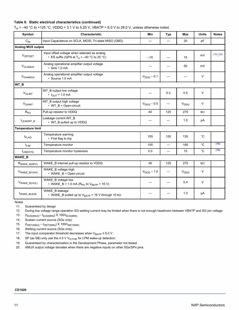
CIN Input Capacitance on SCLK, MOSI, Tri-state MISO (GBD) — — 20 pF
Analog MUX output
VOFFSET Input offset voltage when selected as analog
• ES suffix (QFN at TA = –40 °C to 25 °C) –15 — 15 mV (19),(20)
VOLAMUX Analog operational amplifier output voltage
• Sink 1.0 mA — — 50 mV
VOHAMUX Analog operational amplifier output voltage
• Source 1.0 mA VDDQ – 0.1 — — V
INT_B
VOLINT INT_B output low voltage
• IOUT = 1.0 mA — 0.2 0.5 V
VOHINTINT_B output high voltage
• INT_B = Open-circuit VDDQ – 0.5 — VDDQ V
RPU Pull-up resistor to VDDQ 40 125 270 k
ILEAKINT_B Leakage current INT_B • INT_B pulled up to VDDQ — — 1.0 μA
Temperature limit
tFLAG Temperature warning
• First flag to trip 105 120 135 °C
tLIM Temperature monitor 155 — 185 °C (19)
tLIM(HYS) Temperature monitor hysteresis 5.0 — 15 °C (19)
WAKE_B
RWAKE_B(RPU) WAKE_B internal pull-up resistor to VDDQ 40 125 270 k
VWAKE_B(VOH) WAKE_B voltage high
• WAKE_B = Open-circuit VDDQ – 1.0 — VDDQ V
VWAKE_B(VOL) WAKE_B voltage low
• WAKE_B = 1.0 mA (RPU to VBATP = 16 V) — — 0.4 V
IWAKE_BLEAK WAKE_B leakage
• WAKE_B pulled up to VBATP = 16 V through 10 k — — 1.0 μA
Notes11. Guaranteed by design12. During low voltage range operation SG wetting current may be limited when there is not enough headroom between VBATP and SG pin voltage. 13. (ISUS(MAX)– ISUS(MIN)) X 100/ISUS(MIN)14. Sustain current source (SGs only)15. (IWET(MAX) – IWET(MIN)) X 100/IWET(MIN)16. Wetting current source (SGs only)17. The input comparator threshold decreases when VBATP ≤ 6.0 V.18. SP (as SB) only use the 4.0 V VICTHR for LPM wake-up detection.19. Guaranteed by characterization in the Development Phase, parameter not tested.20. AMUX output voltage deviates when there are negative inputs on other SGx/SPx pins.
Table 6. Static electrical characteristics (continued)TA = –40 °C to +125 °C, VDDQ = 3.1 V to 5.25 V, VBATP = 6.0 V to 28.0 V, unless otherwise noted.
Symbol Characteristic Min Typ Max Units Notes
11 NXP Semiconductors
CD1020
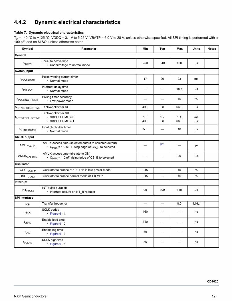
4.4.2 Dynamic electrical characteristics
Table 7. Dynamic electrical characteristics TA = –40 °C to +125 °C, VDDQ = 3.1 V to 5.25 V, VBATP = 6.0 V to 28 V, unless otherwise specified. All SPI timing is performed with a 100 pF load on MISO, unless otherwise noted.
Symbol Parameter Min Typ Max Units Notes
General
tACTIVE POR to active time
• Undervoltage to normal mode 250 340 450 μs
Switch input
tPULSE(ON)Pulse wetting current timer
• Normal mode 17 20 23 ms
tINT-DLYInterrupt delay time
• Normal mode — — 18.5 μs
tPOLLING_TIMERPolling timer accuracy
• Low-power mode — — 15 %
tACTIVEPOLLSGTIME Tactivepoll timer SG 49.5 58 66.5 μs
tACTIVEPOLLSBTIME
Tactivepoll timer SB• SBPOLLTIME = 0• SBPOLLTIME = 1
1.049.5
1.258
1.466.5
msμs
tGLITCHTIMERInput glitch filter timer
• Normal mode 5.0 — 18 μs
AMUX output
AMUXVALID AMUX access time (selected output to selected output)
• CMUX = 1.0 nF, Rising edge of CS_B to selected — (22) — μs
AMUXVALIDTS AMUX access time (tri-state to ON)
• CMUX = 1.0 nF, rising edge of CS_B to selected — — 20 μs
Oscillator
OSCTOLLPM Oscillator tolerance at 192 kHz in low-power Mode –15 — 15 %
OSCTOLNOR Oscillator tolerance normal mode at 4.0 MHz –15 — 15 %
Interrupt
INTPULSE INT pulse duration• Interrupt occurs or INT_B request 90 100 110 μs
SPI interface
fOP Transfer frequency — — 8.0 MHz
tSCKSCLK period
• Figure 6 - 1 160 — — ns
tLEADEnable lead time
• Figure 6 - 2 140 — — ns
tLAGEnable lag time
• Figure 6 - 3 50 — — ns
tSCKHSSCLK high time
• Figure 6 - 4 56 — — ns
NXP Semiconductors 12
CD1020
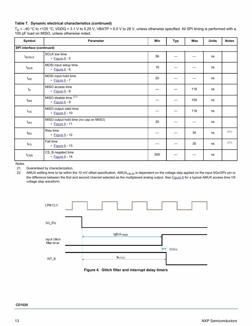
Figure 4. Glitch filter and interrupt delay timers
SPI interface (continued)
tSCKLSSCLK low time
• Figure 6 - 5 56 — — ns
tSUSMOSI input setup time
• Figure 6 - 6 16 — — ns
tHSMOSI input hold time
• Figure 6 - 7 20 — — ns
tAMISO access time
• Figure 6 - 8 — — 116 ns
tDISMISO disable time (21)
• Figure 6 - 9 — — 100 ns
tVSMISO output valid time
• Figure 6 - 10 — — 116 ns
tHOMISO output hold time (no cap on MISO)
• Figure 6 - 11 20 — — ns
tRORise time
• Figure 6 - 12 — — 30 ns (21)
tFOFall time
• Figure 6 - 13 — — 30 ns (21)
tCSNCS_B negated time
• Figure 6 - 14 500 — — ns
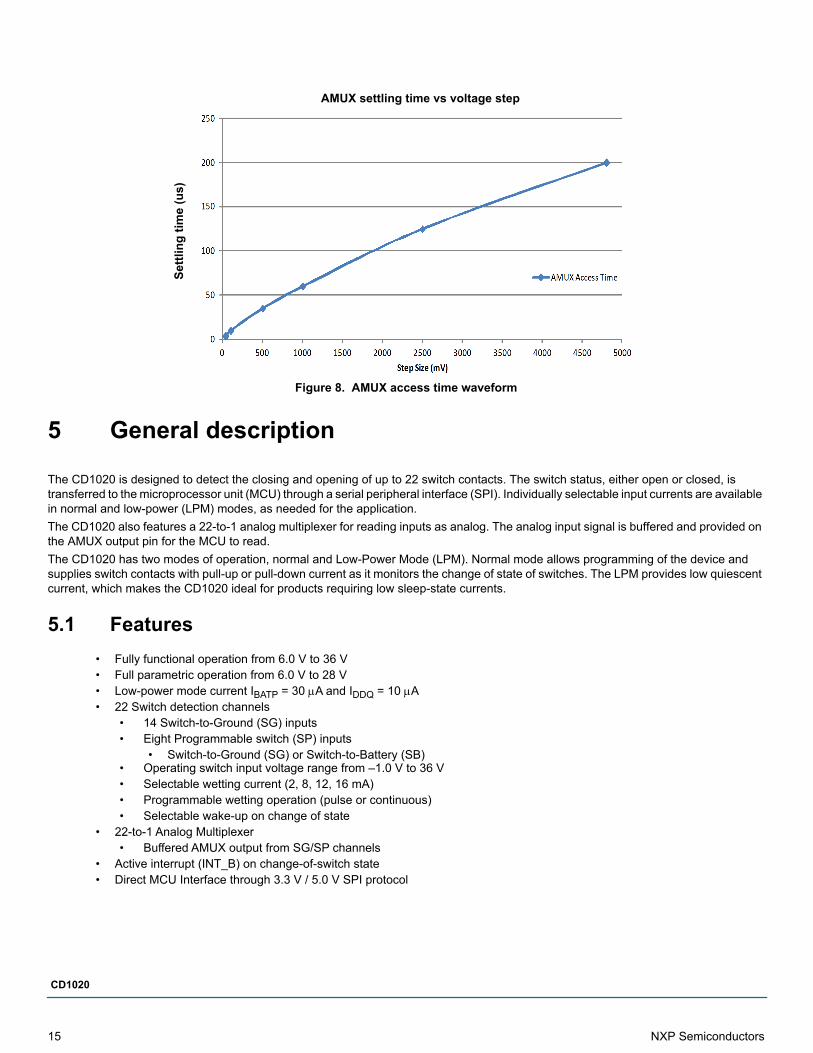
Notes 21. Guaranteed by characterization.22. AMUX settling time to be within the 10 mV offset specification. AMUXVALID is dependent on the voltage step applied on the input SGx/SPx pin or
the difference between the first and second channel selected as the multiplexed analog output. See Figure 8 for a typical AMUX access time VS voltage step waveform.
Table 7. Dynamic electrical characteristics (continued)TA = –40 °C to +125 °C, VDDQ = 3.1 V to 5.25 V, VBATP = 6.0 V to 28 V, unless otherwise specified. All SPI timing is performed with a 100 pF load on MISO, unless otherwise noted.
Symbol Parameter Min Typ Max Units Notes
13 NXP Semiconductors
CD1020
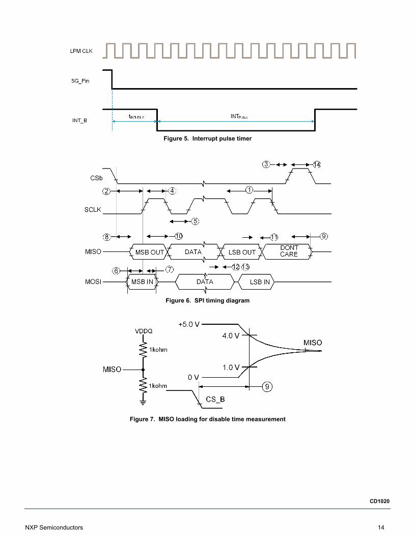
Figure 5. Interrupt pulse timer
Figure 6. SPI timing diagram
Figure 7. MISO loading for disable time measurement
NXP Semiconductors 14
CD1020
Settl
ing
time
(us)
AMUX settling time vs voltage step
Figure 8. AMUX access time waveform
5 General description
The CD1020 is designed to detect the closing and opening of up to 22 switch contacts. The switch status, either open or closed, is transferred to the microprocessor unit (MCU) through a serial peripheral interface (SPI). Individually selectable input currents are available in normal and low-power (LPM) modes, as needed for the application.The CD1020 also features a 22-to-1 analog multiplexer for reading inputs as analog. The analog input signal is buffered and provided on the AMUX output pin for the MCU to read.The CD1020 has two modes of operation, normal and Low-Power Mode (LPM). Normal mode allows programming of the device and supplies switch contacts with pull-up or pull-down current as it monitors the change of state of switches. The LPM provides low quiescent current, which makes the CD1020 ideal for products requiring low sleep-state currents.
5.1 Features• Fully functional operation from 6.0 V to 36 V• Full parametric operation from 6.0 V to 28 V • Low-power mode current IBATP = 30 A and IDDQ = 10 A• 22 Switch detection channels
• 14 Switch-to-Ground (SG) inputs• Eight Programmable switch (SP) inputs
• Switch-to-Ground (SG) or Switch-to-Battery (SB)• Operating switch input voltage range from –1.0 V to 36 V• Selectable wetting current (2, 8, 12, 16 mA)• Programmable wetting operation (pulse or continuous)• Selectable wake-up on change of state
• 22-to-1 Analog Multiplexer • Buffered AMUX output from SG/SP channels
• Active interrupt (INT_B) on change-of-switch state• Direct MCU Interface through 3.3 V / 5.0 V SPI protocol
15 NXP Semiconductors
CD1020
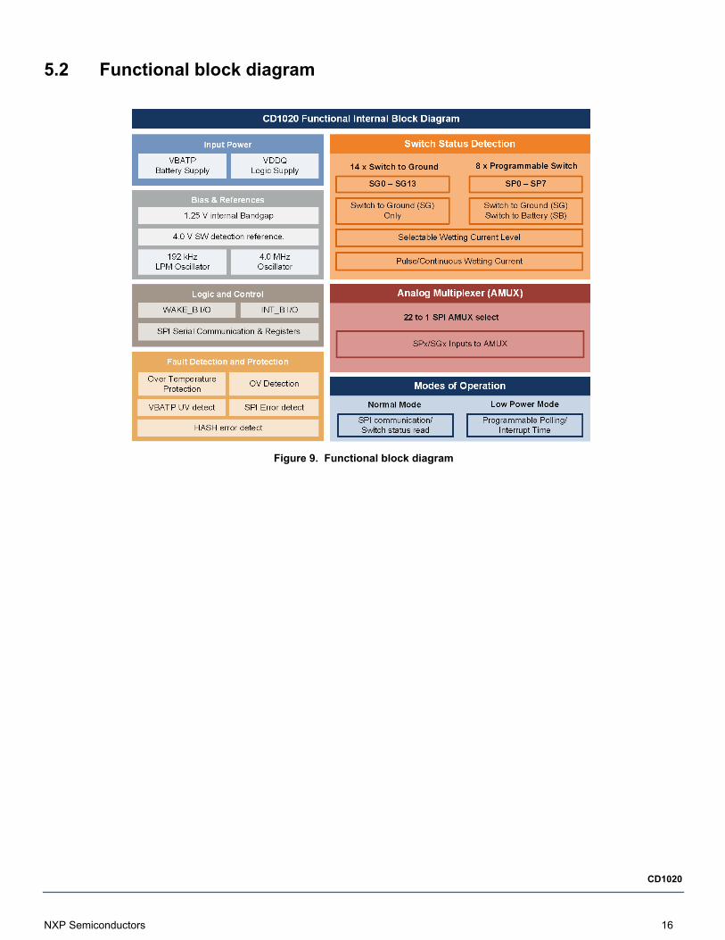
5.2 Functional block diagram
Figure 9. Functional block diagram
NXP Semiconductors 16
CD1020
6 General IC functional description
The CD1020 device interacts with many connections outside the module and near the end user. The IC detects changes in switch state and reports the information to the MCU via the SPI protocol. The input pins generally connect to switches located outside the module and in proximity to battery in car harnesses. Consequently, the IC must have some external protection including an ESD capacitor and series resistors, to ensure the energy from the various pulses are limited at the IC.The IC requires a blocking diode be used on the VBATP pin to protect from a reverse battery condition. The inputs are capable of surviving reverse battery without a blocking diode, due to an internal blocking diode from the input to the power supply (VBATP). This arrangement ensures that there is no backfeeding of voltage/current into the IC, when the voltage on the input is higher than the VBATP pin.
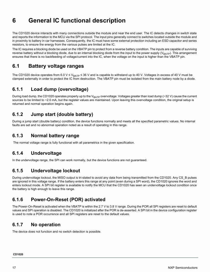
6.1 Battery voltage rangesThe CD1020 device operates from 6.0 V ≤ VBATP ≤ 36 V and is capable to withstand up to 40 V. Voltages in excess of 40 V must be clamped externally in order to protect the IC from destruction. The VBATP pin must be isolated from the main battery node by a diode.
6.1.1 Load dump (overvoltage)During load dump, the CD1020 operates properly up to the VBATP overvoltage. Voltages greater than load dump (~32 V) cause the current sources to be limited to ~2.0 mA, but the register values are maintained. Upon leaving this overvoltage condition, the original setup is returned and normal operation begins again.
6.1.2 Jump start (double battery)During a jump start (double battery) condition, the device functions normally and meets all the specified parametric values. No internal faults are set and no abnormal operation noted as a result of operating in this range.
6.1.3 Normal battery range The normal voltage range is fully functional with all parametrics in the given specification.
6.1.4 UndervoltageIn the undervoltage range, the SPI can work normally, but the device functions are not guaranteed.
6.1.5 Undervoltage lockoutDuring undervoltage lockout, the MISO output is tri-stated to avoid any data from being transmitted from the CD1020. Any CS_B pulses are ignored in this voltage range. If the battery enters this range at any point (even during a SPI word), the CD1020 ignores the word and enters lockout mode. A SPI bit register is available to notify the MCU that the CD1020 has seen an undervoltage lockout condition once the battery is high enough to leave this range.
6.1.6 Power-On-Reset (POR) activatedThe Power-On-Reset is activated when the VBATP is within the 2.7 V to 3.8 V range. During the POR all SPI registers are reset to default values and SPI operation is disabled. The CD1020 is initialized after the POR is de-asserted. A SPI bit in the device configuration register is used to note a POR occurrence and all SPI registers are reset to the default values.
6.1.7 No operationThe device does not function and no switch detection is possible.
17 NXP Semiconductors
CD1020
Figure 10. Battery voltage range
6.2 Power sequencing conditionsThe chip uses two supplies as inputs into the device for various usage. The pins are VBATP and VDDQ. The VBATP pin is the power supply for the chip where the internal supplies are generated and power supply for the SG circuits. The VDDQ pin is used for the I/O buffer supply to talk to the MCU or other logic level devices, as well as AMUX. The INT_B pin is held low upon POR until the IC is ready to operate and communicate. Power can be applied in various ways to the CD1020. The following sections describe the possible states.
6.2.1 VBATP before VDDQThe normal condition for operation is the application of VBATP and then VDDQ. The chip begins to operate logically in the default state but without the ability to drive logic pins. When the VDDQ supply is available, the chip is able to communicate correctly. The IC maintains its logical state (register settings) with functional behavior consistent with logical state. No SPI communications can occur.
6.2.2 VDDQ before VBATPThe VDDQ supply in some cases may be available before the VBATP supply is ready. In this scenario, there is no back feeding current into the VDDQ pin that could potentially turn on the device into an unknown state. VDDQ is isolated from VBATP circuits and the device is off until VBATP is applied; when VBATP is available the device powers up the internal rails and logic within tACTIVE time. Communication is undefined until the tACTIVE time and becomes available after this time frame.
6.2.3 VBATP okay, VDDQ lostAfter power up, it is possible that the VDDQ may turn off or be lost. In this case, the chip remains in the current state but is not able to communicate. After the VDDQ pin is available again, the chip is ready to communicate.
6.2.4 VDDQ okay, VBATP lostAfter power up, the VBATP supply could be lost. The operation is consistent as when VDDQ is available before VBATP.
NXP Semiconductors 18
CD1020
7 Functional block description
7.1 State diagram
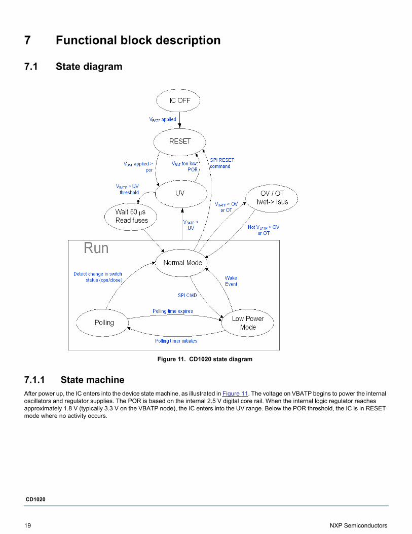
Figure 11. CD1020 state diagram
7.1.1 State machineAfter power up, the IC enters into the device state machine, as illustrated in Figure 11. The voltage on VBATP begins to power the internal oscillators and regulator supplies. The POR is based on the internal 2.5 V digital core rail. When the internal logic regulator reaches approximately 1.8 V (typically 3.3 V on the VBATP node), the IC enters into the UV range. Below the POR threshold, the IC is in RESET mode where no activity occurs.
19 NXP Semiconductors
CD1020
7.1.2 UV: undervoltage lockoutAfter the POR circuit has reset the logic, the IC is in undervoltage. In this state, the IC remembers all register conditions, but is in a lockout mode, where no SPI communication is allowed. The AMUX is inactive and the current sources are off. The user does not receive a valid response from the MISO, as it is disabled in this state. The chip oscillators (4.0 MHz for most normal mode activities, 192 kHz for LPM, and limited normal mode functions) are turned on in the UV state. The chip moves to the Read fuses state when the VBATP voltage rises above the UV threshold (~4.3 V rising). The internal fuses read in approximately 50 s and the chip enters the normal mode.
7.1.3 Normal modeIn normal mode, the chip operates as selected in the available registers. Any command may be loaded in normal mode, although not all (low-power mode) registers are used in the normal mode. All the LPM registers must be programmed in Normal mode as the SPI is not active in LPM. The normal mode of the chip is used to:
• Operate the AMUX• Communicate via the SPI• Interrupt the IC, wetting and sustain currents, and the thresholds available to use
The WAKE_B pin is asserted (low) in normal mode and can be used to enable a power supply (ENABLE_B). Various fault detections are available in this mode including overvoltage, overtemperature, thermal warning, SPI errors, and Hash faults.
7.1.4 Low-power modeWhen the user needs to lower the IC current consumption, a low-power mode is used. The only method to enter LPM is through a SPI word. After the chip is in low-power mode, the majority of circuitry is turned off including most power rails, the 4.0 MHz oscillator, and all the fault detection circuits. This mode is the lowest current consumption mode on the chip. If a fault occurs while the chip is in this mode, the chip does not see or register the fault (does not report via the SPI when awakened). Some items may wake the IC in this mode, including the interrupt timer, falling edge of INT_B, CS_B, or WAKE_B (configurable), or a comparator-only mode switch detection.
7.1.5 Polling modeThe CD1020 uses a polling mode that periodically (selectable in LPM config register) interrogates the input pins to determine in what state the pins are, and decides if there was a change of state from when the chip was in normal mode. There are various configurations for this mode, which allow the user greater flexibility in operation. This mode uses the current sources to pull up (SG) or pull down (SB) to determine if a switch is open or closed. More information is available in section 7.2, “Low-power mode operation". In the case of a low VBATP, the polling pauses and waits until the VBATP rises out of UV or a POR occurs. The pause of the polling ensures all of the internal rails, currents, and thresholds are up at the required levels to accurately detect open or closed switches. The chip does not wake-up in this condition and simply waits for the VBATP voltage to rise or cause a POR. After the polling ends, the chip either returns to the low-power mode, or enters normal mode when a wake event is detected. Other events may wake the chip as well, such as the falling edge of CS_B, INT_B, or WAKE_B (configurable). A comparator only mode switch detection is always on in LPM or Polling mode, therefore, a change of state for those inputs would effectively wake the IC in Polling mode as well.If the Wake-up enable bits are disabled on all channels (SG and SP), the device will not wake up with a change of state on any of the input pins. In this case, the device will disable the polling timer to allow the lowest current consumption during low-power mode.
7.2 Low-power mode operationLow-power mode (LPM) is used to reduce system quiescent currents. LPM may be entered only by sending the Enter Low-power mode command. All register settings programmed in normal mode are maintained while in LPM.The CD1020 exits LPM and enter normal mode when any of the following events occur:
• Input switch change of state (when enabled)• Falling edge of WAKE_B (as set by the device configuration register)• Falling edge of INT_B (with VDDQ = 5.0 V)• Falling edge of CS_B (with VDDQ = 5.0 V)• Power-On-Reset (POR)
The VDDQ supply may be removed from the device during LPM, however removing VDDQ from the device disables a wake-up from falling edge of INT_B and CS_B. The IC checks the status of VDDQ after a falling edge of WAKE_B (as selected in the device configuration
NXP Semiconductors 20
CD1020
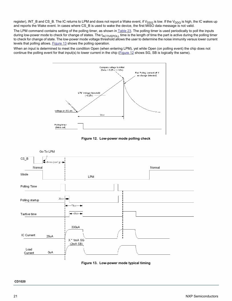
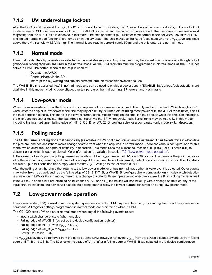
register), INT_B and CS_B. The IC returns to LPM and does not report a Wake event, if VDDQ is low. If the VDDQ is high, the IC wakes up and reports the Wake event. In cases where CS_B is used to wake the device, the first MISO data message is not valid. The LPM command contains setting of the polling timer, as shown in Table 23. The polling timer is used periodically to poll the inputs during low-power mode to check for change of states. The tACTIVEPOLL time is the length of time the part is active during the polling timer to check for change of state. The low-power mode voltage threshold allows the user to determine the noise immunity versus lower current levels that polling allows. Figure 13 shows the polling operation. When an input is determined to meet the condition Open (when entering LPM), yet while Open (on polling event) the chip does not continue the polling event for that input(s) to lower current in the chip (Figure 12 shows SG, SB is logically the same).
Figure 12. Low-power mode polling check
Figure 13. Low-power mode typical timing
21 NXP Semiconductors
CD1020
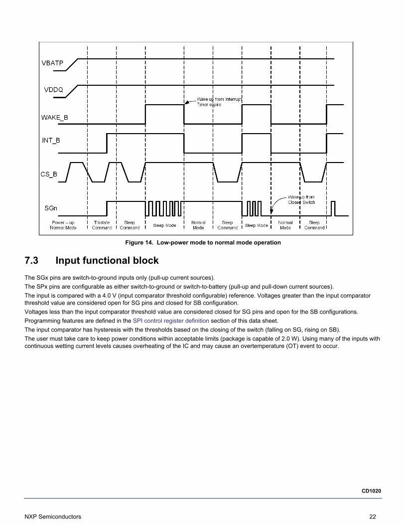
Figure 14. Low-power mode to normal mode operation
7.3 Input functional block The SGx pins are switch-to-ground inputs only (pull-up current sources). The SPx pins are configurable as either switch-to-ground or switch-to-battery (pull-up and pull-down current sources). The input is compared with a 4.0 V (input comparator threshold configurable) reference. Voltages greater than the input comparator threshold value are considered open for SG pins and closed for SB configuration. Voltages less than the input comparator threshold value are considered closed for SG pins and open for the SB configurations. Programming features are defined in the SPI control register definition section of this data sheet. The input comparator has hysteresis with the thresholds based on the closing of the switch (falling on SG, rising on SB).The user must take care to keep power conditions within acceptable limits (package is capable of 2.0 W). Using many of the inputs with continuous wetting current levels causes overheating of the IC and may cause an overtemperature (OT) event to occur.
NXP Semiconductors 22
CD1020
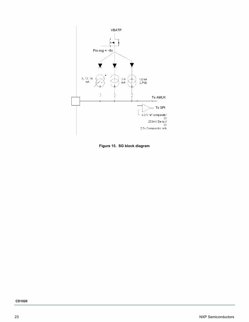
Figure 15. SG block diagram
23 NXP Semiconductors
CD1020
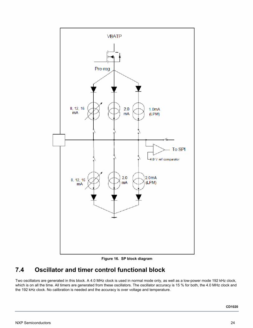
Figure 16. SP block diagram
7.4 Oscillator and timer control functional blockTwo oscillators are generated in this block. A 4.0 MHz clock is used in normal mode only, as well as a low-power mode 192 kHz clock, which is on all the time. All timers are generated from these oscillators. The oscillator accuracy is 15 % for both, the 4.0 MHz clock and the 192 kHz clock. No calibration is needed and the accuracy is over voltage and temperature.
NXP Semiconductors 24
CD1020
7.5 Temperature monitor and control functional blockThe device has multiple thermal limit (tLIM) cells to detect thermal excursions in excess of 155 °C. The tLIM cells from various locations on the IC are logically ORed together and communicated to the MCU as one tLIM fault. When the tLIM value is seen, the wetting current is lowered to 2.0 mA until the temperature has decreased beyond the tLIM(HYS) value (the sustain current remains on or as selected). A hysteresis value of 15 °C exists to keep the device from cycling. A thermal flag also exists to alert the system to increasing temperatures more than approximately 120 °C.
7.6 WAKE_B control functional blockThe WAKE_B pin can operate as an open-drain output or a wake-up input. In the normal mode, the WAKE_B pin is LOW. In the low- power mode, the WAKE_B pin is pulled HIGH. The WAKE_B pin has an internal pull-up to VDDQ supply with an internal series diode to allow an external pull-up to VBATP if required.As an input, in low-power mode with the WAKE_B pin pulled HIGH, when commanded LOW by MCU, the falling edge of WAKE_B places the CD1020 in normal mode. In low-power mode if VDDQ goes low, the WAKE_B pin can still wake the device based on the status of the WAKE_B bit in the device configuration register, this allows the user to pull the WAKE_B pin up to VBATP such that it can be used in VDDQ off setup.As an output, WAKE_B pin can drive either an MCU input or the EnableB of a regulator (possibly for VDDQ). WAKE_B is driven low during normal mode regardless of the state of VDDQ. When the CD1020 is in LPM, the WAKE_B pin is released and is expected to be pulled up internally to VDDQ or externally to VBATP. When a valid wake-up event is detected, the CD1020 wakes up from LPM and the WAKE_B is driven Low (regardless of the state of VDDQ).
7.7 INT_B functional blockINT_B is an input/output pin in the CD1020 device to indicate an interrupt event has occurred, as well as receiving interrupts from other devices when the INT_B pins are wired ORed. The INT_B pin is an open-drain output with an internal pull-up to VDDQ. In normal mode, a switch state change triggers the INT_B pin (when enabled). The INT_B pin and INT_B bit in the SPI register are latched on the falling edge of CS_B. This permits the MCU to determine the origin of the interrupt. When two CD1020 devices are used, only the device initiating the interrupt has the INT_B bit set. The INT_B pin and INTflg bit are cleared 1.0 s after the falling edge of CS B. The INT_B pin does not clear with the rising edge of CS_B if a switch contact change has occurred while CS_B was Low.In a multiple CD1020 device system with WAKE_B High and VDDQ on (low-power mode), the falling edge of INT_B places the device in normal mode. The INT_B has the option of a pulsed output (pulsed low for INTpulse duration) or a latched low output. The default case is the latched low operation; the pulsed option is selectable via the SPI.An INT_B request by the MCU can be done by a SPI word and results in an INTPULSE of 100 s duration on the INT_B pin. The chip causes an INT_B assertion for the following cases:
• A change of state is detected• Any Wake-up event• Any faults detected• After a POR, the INT_B pin states asserted during startup until the chip is ready to communicate
7.8 AMUX functional blockThe analog voltage-on-switch inputs may be read by the MCU using the analog command. See Table 36. Internal to the IC is a 22-to-1 analog multiplexer. The voltage present on the selected input pin is buffered and made available on the AMUX output pin. The output pin is clamped to a maximum of VDDQ, regardless of the higher voltages present on the input pin. After an input has been selected as the analog, the corresponding bit in the next MISO data stream is logic [0]. When selecting a channel to be read as analog input, the user can also set the current level allowed in the AMUX output. Current level can be set to the programmed wetting current for the selected channel or set to high impedance as defined in Table 35. When selecting an input to be sent to the AMUX output, that input is not polled or a wake-up enabled input from low-power mode. The user should set the AMUX to ‘No input selected’ before entering low-power mode. The AMUX pin is not active during low-power mode.
25 NXP Semiconductors
CD1020
7.9 Serial peripheral interface (SPI)The CD1020 contains a serial peripheral interface consisting of Serial Clock (SCLK), Serial Data Out (MISO), Serial Data In (MOSI), and Chip Select Bar (CS_B). The SPI interface is used to provide configuration, control, and status functions; the user may read the registers’ contents as well as read some status bits of the IC. This device is configured as a SPI slave. All SPI transmissions to the CD1020 must be done in exact increments of 32 bits (modulo 0 is ignored as well). The CD1020 contains a data valid method via SCLK input to keep non-modulo 32-bit transmissions from being written into the IC. The SPI module also provides a daisy chain capability to accommodate MOSI to MISO wrap around (see Figure 20).The SPI registers have a hashing technique to ensure that the registers are consistent with the programmed values. If the hashed value does not match the register status, a SPI bit is set as well as an interrupt to alert the MCU to this issue.
7.9.1 Chip select low (CS_B)The CS_B input selects this device for serial transfers. On the falling edge of CS_B, the MISO pin is released from tri-state mode, and all status information are latched in the SPI shift register. While CS_B is asserted, register data is shifted in the MOSI pin and shifted out the MISO pin on each subsequent SCLK. On the rising edge of CS_B, the MISO pin is tri-stated and the fault register reloaded (latched) with the current filtered status data. To allow sufficient time to reload the fault registers, the CS_B pin must remain low for a minimum of tCSN prior to going high again. The CS_B input contains a pull-up current source to VDDQ to command the de-asserted state should an open-circuit condition occur. This pin has threshold compatible voltages allowing proper operation with microprocessors using a 3.3 V to 5.0 V supply.
7.9.2 Serial clock (SCLK)The SCLK input is the clock signal input for synchronization of serial data transfer. This pin has threshold-compatible voltages allowing proper operation with microprocessors using a 3.3 V to 5.0 V supply.When CS_B is asserted, both the Master Microprocessor and this device latch input data on the rising edge of SCLK. The SPI master typically shifts data out on the falling edge of SCLK, while this device shifts data out on the rising edge of SCLK, to allow more time to drive the MISO pin to the proper level. This input is used as the input for the modulo 32-bit counter validation. Any SPI transmissions which are NOT exact multiples of 32 bits (i.e. clock edges) is treated as an illegal transmission. The entire frame is aborted and no information is changed in the configuration or control registers.
7.9.3 Serial data output (MISO)The MISO output pin is in a tri-state condition when CS_B is negated. When CS_B is asserted, MISO is driven to the state of the MSB of the internal register and start shifting out the requested data from the MSB to the LSB. This pin supplies a ‘rail to rail’ output, depending on the voltage at the VDDQ pin.
7.9.4 Serial data input (MOSI)The MOSI input takes data from the master microprocessor while CS_B is asserted. The MSB is the first bit of each word received on MOSI and the LSB is the last bit of each word received on MOSI. This pin has threshold-level compatible input voltages allowing proper operation with microprocessors using a 3.3 V to 5.0 V (VDDQ) supply.
NXP Semiconductors 26
CD1020
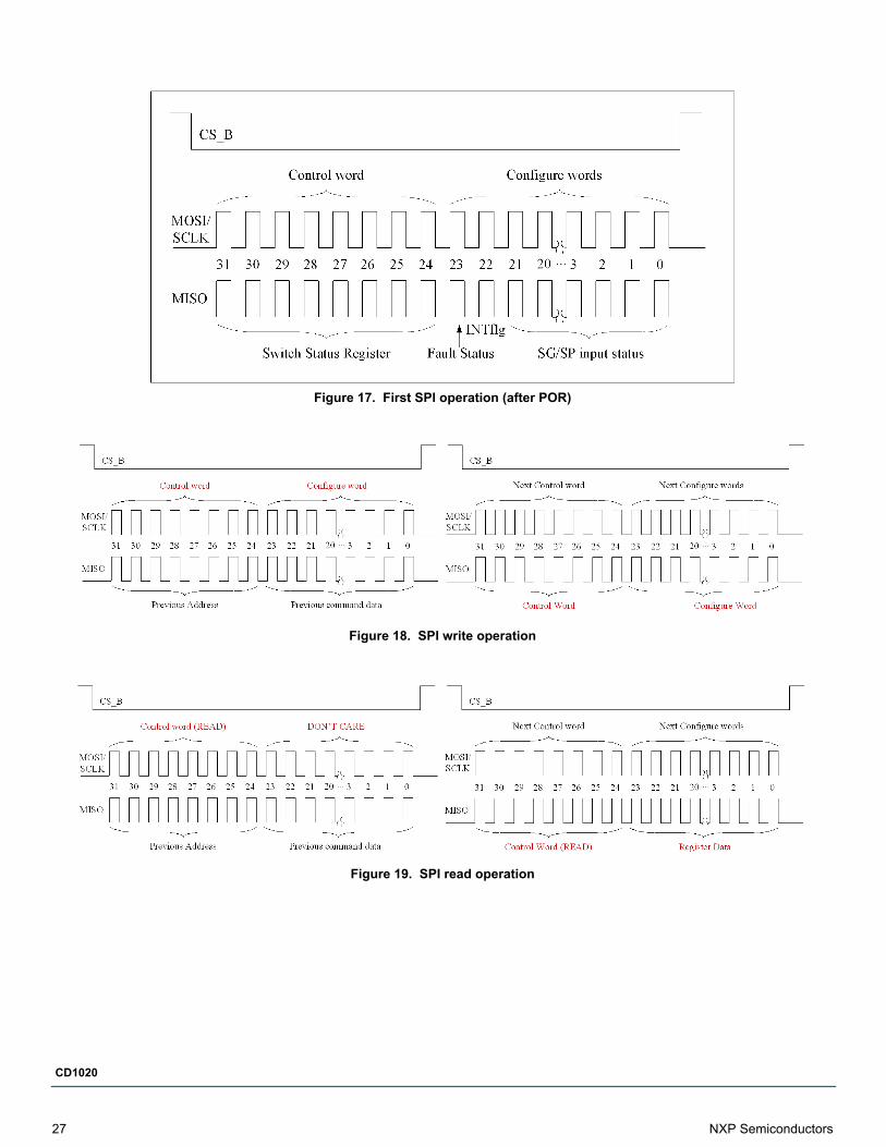
Figure 17. First SPI operation (after POR)
Figure 18. SPI write operation
Figure 19. SPI read operation
27 NXP Semiconductors
CD1020
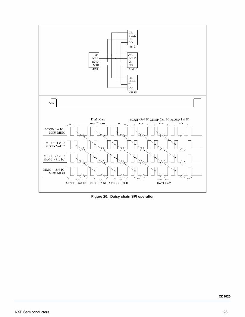
Figure 20. Daisy chain SPI operation
NXP Semiconductors 28
CD1020
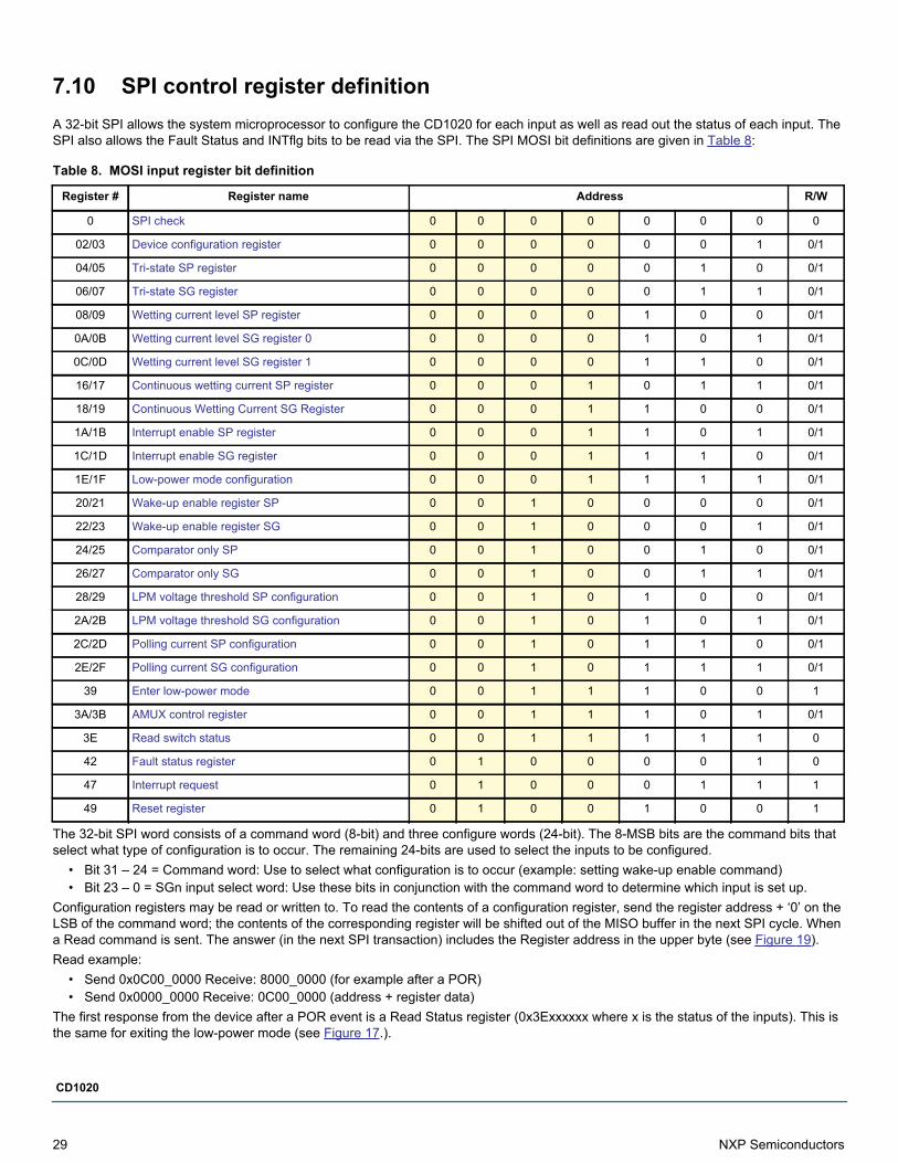
7.10 SPI control register definitionA 32-bit SPI allows the system microprocessor to configure the CD1020 for each input as well as read out the status of each input. The SPI also allows the Fault Status and INTflg bits to be read via the SPI. The SPI MOSI bit definitions are given in Table 8:
Table 8. MOSI input register bit definition
Register # Register name Address R/W
The 32-bit SPI word consists of a command word (8-bit) and three configure words (24-bit). The 8-MSB bits are the command bits that select what type of configuration is to occur. The remaining 24-bits are used to select the inputs to be configured.
• Bit 31 – 24 = Command word: Use to select what configuration is to occur (example: setting wake-up enable command) • Bit 23 – 0 = SGn input select word: Use these bits in conjunction with the command word to determine which input is set up.
Configuration registers may be read or written to. To read the contents of a configuration register, send the register address + ‘0’ on the LSB of the command word; the contents of the corresponding register will be shifted out of the MISO buffer in the next SPI cycle. When a Read command is sent. The answer (in the next SPI transaction) includes the Register address in the upper byte (see Figure 19).Read example:
• Send 0x0C00_0000 Receive: 8000_0000 (for example after a POR)• Send 0x0000_0000 Receive: 0C00_0000 (address + register data)
The first response from the device after a POR event is a Read Status register (0x3Exxxxxx where x is the status of the inputs). This is the same for exiting the low-power mode (see Figure 17.).
0 SPI check 0 0 0 0 0 0 0 0
02/03 Device configuration register 0 0 0 0 0 0 1 0/1
04/05 Tri-state SP register 0 0 0 0 0 1 0 0/1
06/07 Tri-state SG register 0 0 0 0 0 1 1 0/1
08/09 Wetting current level SP register 0 0 0 0 1 0 0 0/1
0A/0B Wetting current level SG register 0 0 0 0 0 1 0 1 0/1
0C/0D Wetting current level SG register 1 0 0 0 0 1 1 0 0/1
16/17 Continuous wetting current SP register 0 0 0 1 0 1 1 0/1
18/19 Continuous Wetting Current SG Register 0 0 0 1 1 0 0 0/1
1A/1B Interrupt enable SP register 0 0 0 1 1 0 1 0/1
1C/1D Interrupt enable SG register 0 0 0 1 1 1 0 0/1
1E/1F Low-power mode configuration 0 0 0 1 1 1 1 0/1
20/21 Wake-up enable register SP 0 0 1 0 0 0 0 0/1
22/23 Wake-up enable register SG 0 0 1 0 0 0 1 0/1
24/25 Comparator only SP 0 0 1 0 0 1 0 0/1
26/27 Comparator only SG 0 0 1 0 0 1 1 0/1
28/29 LPM voltage threshold SP configuration 0 0 1 0 1 0 0 0/1
2A/2B LPM voltage threshold SG configuration 0 0 1 0 1 0 1 0/1
2C/2D Polling current SP configuration 0 0 1 0 1 1 0 0/1
2E/2F Polling current SG configuration 0 0 1 0 1 1 1 0/1
39 Enter low-power mode 0 0 1 1 1 0 0 1
3A/3B AMUX control register 0 0 1 1 1 0 1 0/1
3E Read switch status 0 0 1 1 1 1 1 0
42 Fault status register 0 1 0 0 0 0 1 0
47 Interrupt request 0 1 0 0 0 1 1 1
49 Reset register 0 1 0 0 1 0 0 1
29 NXP Semiconductors
CD1020
To write into a configuration register, send the register Address + ‘1’ on the LSB of the command word and the configuration data on the next 24 bits. The new value of the register will be shifted out of the MISO buffer in the next SPI cycle, along with the register address.Table 9 provides a general overview of the functional SPI commands and configuration bits.
Table 9. Functional SPI register map
23. FS = FAULT STATUS (available for reading on MISO return word)24. INT = INTflg (available for reading on MISO return word)
Commands [31-25] 24 23 22 21 20 19 18 17 16 15 14 13 12 11 10 9 8 7 6 5 4 3 2 1 0
Address R/W
SPI check 0000000 0 X X X X X X X X X X X X X X X X X X X X X X X X
Device Configuration 0000001 0/1 FS INT X X X X X X X X
SBPO
LL T
IME
VBAT
P O
V D
isab
le
WAK
E_B
Pull
up
IntB
_Out
X X SP7
SP6
SP5
SP4
SP3
SP2
SP1
SP0
Tri-State Enable SP 0000010 0/1 FS INT X X X X X X X X X X X X X X SP7 SP6 SP5 SP4 SP3 SP2 SP1 SP0
Tri-State Enable SG 0000011 0/1 FS INT X X X X X X X X SG13 SG12 SG11 SG10 SG9 SG8 SG7 SG6 SG5 SG4 SG3 SG2 SG1 SG0
Wetting Current Level SP 0000100 0/1 SP7[2-0] SP6[2-0] SP5[2-0] SP4[2-0] SP3[2-0] SP2[2-0] SP1[2-0] SP0[2-0]
Wetting Current Level SG 0 0000101 0/1 SG7[2-0] SG6[2-0] SG5[2-0] SG4[2-0] SG3[2-0] SG2[2-0] SG1[2-0] SG0[2-0]
Wetting Current Level SG 1 0000110 0/1 FS INT X X X X SG13[2-0] SG12[2-0] SG11[2-0] SG10[2-0] SG9[2-0] SG8[2-0]
Continuous Wetting Current Enable SP 0001011 0/1 FS INT X X X X X X X X X X X X X X SP7 SP6 SP5 SP4 SP3 SP2 SP1 SP0
Continuous Wetting Current Enable SG 0001100 0/1 FS INT X X X X X X X X SG13 SG12 SG11 SG10 SG9 SG8 SG7 SG6 SG5 SG4 SG3 SG2 SG1 SG0
Interrupt Enable SP 0001101 0/1 FS INT X X X X X X X X X X X X X X SP7 SP6 SP5 SP4 SP3 SP2 SP1 SP0
Interrupt Enable SG 0001110 0/1 FS INT X X X X X X X X SG13 SG12 SG11 SG10 SG9 SG8 SG7 SG6 SG5 SG4 SG3 SG2 SG1 SG0
Low-power mode configuration 0001111 0/1 FS INT X X X X X X X X X X X X X X X X X X poll3 poll2 poll1 poll0
Wake-Up Enable SP 0010000 0/1 FS INT X X X X X X X X X X X X X X SP7 SP6 SP5 SP4 SP3 SP2 SP1 SP0
Wake-Up Enable SG 0010001 0/1 FS INT X X X X X X X X SG13 SG12 SG11 SG10 SG9 SG8 SG7 SG6 SG5 SG4 SG3 SG2 SG1 SG0
LPM Comparator Only SP 0010010 0/1 FS INT X X X X X X X X X X X X X X SP7 SP6 SP5 SP4 SP3 SP2 SP1 SP0
LPM Comparator Only SG 0010011 0/1 FS INT X X X X X X X X SG13 SG12 SG11 SG10 SG9 SG8 SG7 SG6 SG5 SG4 SG3 SG2 SG1 SG0
LPM Voltage Threshold SP 0010100 0/1 FS INT X X X X X X X X X X X X X X SP7 SP6 SP5 SP4 SP3 SP2 SP1 SP0
LPM Voltage Threshold SG 0010101 0/1 FS INT X X X X X X X X SG13 SG12 SG11 SG10 SG9 SG8 SG7 SG6 SG5 SG4 SG3 SG2 SG1 SG0
LPM Polling current config SP 0010110 0/1 FS INT X X X X X X X X X X X X X X SP7 SP6 SP5 SP4 SP3 SP2 SP1 SP0
LPM Polling current config SG 0010111 0/1 FS INT X X X X X X X X SG13 SG12 SG11 SG10 SG9 SG8 SG7 SG6 SG5 SG4 SG3 SG2 SG1 SG0
Enter Low-power mode 0011100 1 FS INT X X X X X X X X X X X X X X X X X X X X X X
AMUX Channel Select SPI 0011101 0/1 FS INT X X X X X X X X X X X X X X X asett asel5 asel4 asel3 asel2 asel1 asel0
Read Switch Status 0011111 0
FAU
LT S
TATU
S
INTf
lg
SP7
SP6
SP5
SP4
SP3
SP2
SP1
SP0
SG13
SG12
SG11
SG10
SG9
SG8
SG7
SG6
SG5
SG4
SG3
SG2
SG1
SG0
Fault Status 0100001 0 X
INTf
lg
X X X X X X X X X X X
SPI E
rror
hash
faul
t
X UV
OV
Tem
pFla
g
OT
INT_
B w
ake
WAK
E_B
SpiW
ake
POR
Interrupt Pulse Request 0100011 1 FS INT X X X X X X X X X X X X X X X X X X X X X X
Reset 0100100 1 X X X X X X X X X X X X X X X X X X X X X X X X
Notes
NXP Semiconductors 30
CD1020
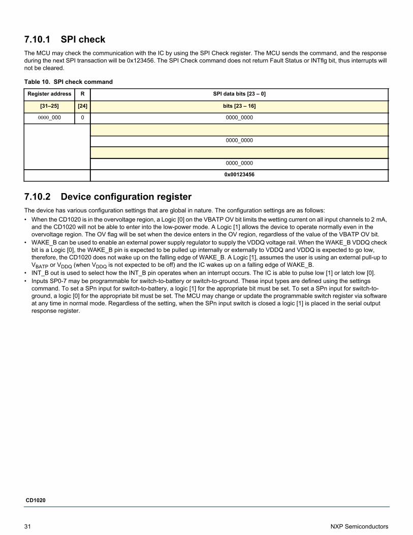
7.10.1 SPI checkThe MCU may check the communication with the IC by using the SPI Check register. The MCU sends the command, and the response during the next SPI transaction will be 0x123456. The SPI Check command does not return Fault Status or INTflg bit, thus interrupts will not be cleared.
Table 10. SPI check command
Register address R SPI data bits [23 – 0]
[31–25] [24] bits [23 – 16]
bits [15 – 8]
bits [7 – 0]
MISO return word 0x00123456
7.10.2 Device configuration registerThe device has various configuration settings that are global in nature. The configuration settings are as follows:• When the CD1020 is in the overvoltage region, a Logic [0] on the VBATP OV bit limits the wetting current on all input channels to 2 mA,
and the CD1020 will not be able to enter into the low-power mode. A Logic [1] allows the device to operate normally even in the overvoltage region. The OV flag will be set when the device enters in the OV region, regardless of the value of the VBATP OV bit.
• WAKE_B can be used to enable an external power supply regulator to supply the VDDQ voltage rail. When the WAKE_B VDDQ check bit is a Logic [0], the WAKE_B pin is expected to be pulled up internally or externally to VDDQ and VDDQ is expected to go low, therefore, the CD1020 does not wake up on the falling edge of WAKE_B. A Logic [1], assumes the user is using an external pull-up to VBATP or VDDQ (when VDDQ is not expected to be off) and the IC wakes up on a falling edge of WAKE_B.
• INT_B out is used to select how the INT_B pin operates when an interrupt occurs. The IC is able to pulse low [1] or latch low [0].• Inputs SP0-7 may be programmable for switch-to-battery or switch-to-ground. These input types are defined using the settings
command. To set a SPn input for switch-to-battery, a logic [1] for the appropriate bit must be set. To set a SPn input for switch-to-ground, a logic [0] for the appropriate bit must be set. The MCU may change or update the programmable switch register via software at any time in normal mode. Regardless of the setting, when the SPn input switch is closed a logic [1] is placed in the serial output response register.
0000_000 0 0000_0000
0000_0000
0000_0000
31 NXP Semiconductors
CD1020
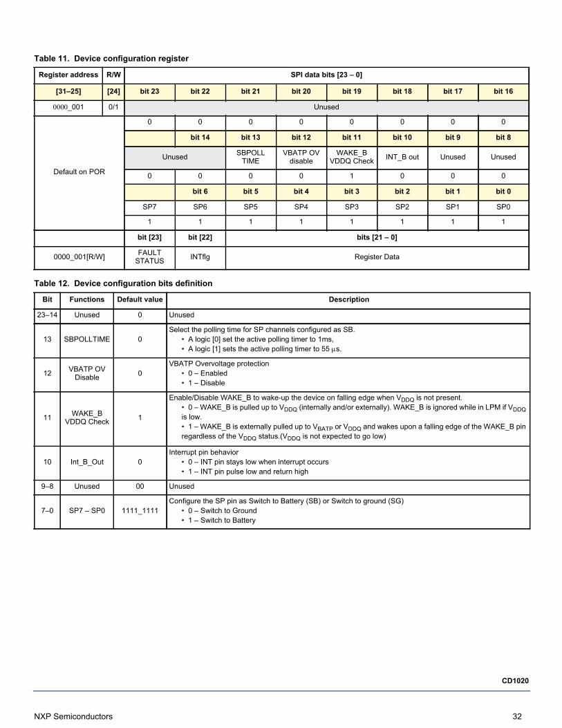
Table 11. Device configuration register
Register address R/W SPI data bits [23 – 0]
[31–25] [24] bit 23 bit 22 bit 21 bit 20 bit 19 bit 18 bit 17 bit 16
bit 15 bit 14 bit 13 bit 12 bit 11 bit 10 bit 9 bit 8
bit 7 bit 6 bit 5 bit 4 bit 3 bit 2 bit 1 bit 0
MISO return word bit [23] bit [22] bits [21 – 0]
Table 12. Device configuration bits definition
Bit Functions Default value Description
• A logic [0] set the active polling timer to 1ms, • A logic [1] sets the active polling timer to 55 s.
• 0 – Enabled• 1 – Disable
• 0 – WAKE_B is pulled up to VDDQ (internally and/or externally). WAKE_B is ignored while in LPM if VDDQ is low.• 1 – WAKE_B is externally pulled up to VBATP or VDDQ and wakes upon a falling edge of the WAKE_B pin regardless of the VDDQ status.(VDDQ is not expected to go low)
• 0 – INT pin stays low when interrupt occurs• 1 – INT pin pulse low and return high
• 0 – Switch to Ground• 1 – Switch to Battery
0000_001 0/1 Unused
Default on POR
0 0 0 0 0 0 0 0
Unused SBPOLL TIME
VBATP OV disable
WAKE_B VDDQ Check INT_B out Unused Unused
0 0 0 0 1 0 0 0
SP7 SP6 SP5 SP4 SP3 SP2 SP1 SP0
1 1 1 1 1 1 1 1
0000_001[R/W] FAULT STATUS INTflg Register Data
23–14 Unused 0 Unused
13 SBPOLLTIME 0Select the polling time for SP channels configured as SB.
12 VBATP OV Disable 0
VBATP Overvoltage protection
11 WAKE_B VDDQ Check 1
Enable/Disable WAKE_B to wake-up the device on falling edge when VDDQ is not present.
10 Int_B_Out 0Interrupt pin behavior
9–8 Unused 00 Unused
7–0 SP7 – SP0 1111_1111Configure the SP pin as Switch to Battery (SB) or Switch to ground (SG)
NXP Semiconductors 32
CD1020
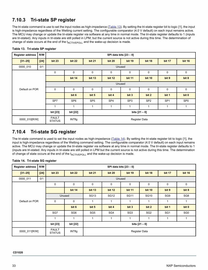
7.10.3 Tri-state SP register The tri-state command is use to set the input nodes as high-impedance (Table 13). By setting the tri-state register bit to logic [1], the input is high-impedance regardless of the Wetting current setting. The configurable comparator (4.0 V default) on each input remains active. The MCU may change or update the tri-state register via software at any time in normal mode. The tri-state register defaults to 1 (inputs are tri-stated). Any inputs in tri-state are still polled in LPM, but the current source is not active during this time. The determination of change of state occurs at the end of the tACTIVEPOLL and the wake-up decision is made.
Table 13. Tri-state SP register
Register address R/W SPI data bits [23 – 0]
[31–25] [24] bit 23 bit 22 bit 21 bit 20 bit 19 bit 18 bit 17 bit 16
bit 15 bit 14 bit 13 bit 12 bit 11 bit 10 bit 9 bit 8
bit 7 bit 6 bit 5 bit 4 bit 3 bit 2 bit 1 bit 0
MISO return word bit [23] bit [22] bits [21 – 0]
7.10.4 Tri-state SG registerThe tri-state command is used to set the input nodes as high-impedance (Table 14). By setting the tri-state register bit to logic [1], the input is high-impedance regardless of the Wetting command setting. The configurable comparator (4.0 V default) on each input remains active. The MCU may change or update the tri-state register via software at any time in normal mode. The tri-state register defaults to 1 (inputs are tri-stated. Any inputs in tri-state are still polled in LPM but the current source is not active during this time. The determination of change of state occurs at the end of the tACTIVEPOLL and the wake-up decision is made.
Table 14. Tri-state SG register
Register address R/W SPI data bits [23 – 0]
[31–25] [24] bit 23 bit 22 bit 21 bit 20 bit 19 bit 18 bit 17 bit 16
bit 15 bit 14 bit 13 bit 12 bit 11 bit 10 bit 9 bit 8
bit 7 bit 6 bit 5 bit 4 bit 3 bit 2 bit 1 bit 0
MISO return word bit [23] bit [22] bits [21 – 0]
0000_010 0/1 Unused
Default on POR
0 0 0 0 0 0 0 0
Unused
0 0 0 0 0 0 0 0
SP7 SP6 SP5 SP4 SP3 SP2 SP1 SP0
1 1 1 1 1 1 1 1
0000_010[R/W] FAULT STATUS INTflg Register Data
0000_011 0/1 Unused
Default on POR
0 0 0 0 0 0 0 0
Unused SG13 SG12 SG11 SG10 SG9 SG8
0 0 1 1 1 1 1 1
SG7 SG6 SG5 SG4 SG3 SG2 SG1 SG0
1 1 1 1 1 1 1 1
0000_011[R/W] FAULT STATUS INTflg Register Data
33 NXP Semiconductors
CD1020
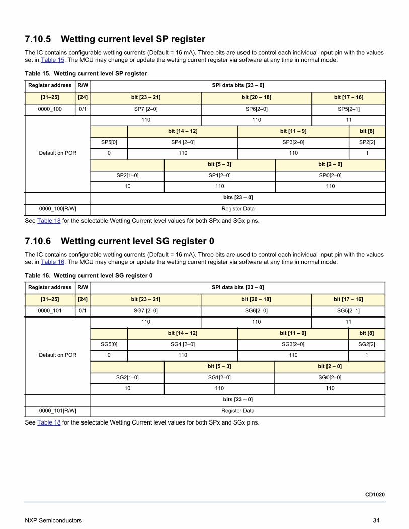
7.10.5 Wetting current level SP registerThe IC contains configurable wetting currents (Default = 16 mA). Three bits are used to control each individual input pin with the values set in Table 15. The MCU may change or update the wetting current register via software at any time in normal mode.
Table 15. Wetting current level SP register
Register address R/W SPI data bits [23 – 0]
[31–25] [24] bit [23 – 21] bit [20 – 18] bit [17 – 16]
bit [15] bit [14 – 12] bit [11 – 9] bit [8]
bit [7 – 6] bit [5 – 3] bit [2 – 0]
MISO return word bits [23 – 0]
See Table 18 for the selectable Wetting Current level values for both SPx and SGx pins.
7.10.6 Wetting current level SG register 0The IC contains configurable wetting currents (Default = 16 mA). Three bits are used to control each individual input pin with the values set in Table 16. The MCU may change or update the wetting current register via software at any time in normal mode.
Table 16. Wetting current level SG register 0
Register address R/W SPI data bits [23 – 0]
[31–25] [24] bit [23 – 21] bit [20 – 18] bit [17 – 16]
bit [15] bit [14 – 12] bit [11 – 9] bit [8]
bit [7 – 6] bit [5 – 3] bit [2 – 0]
MISO return word bits [23 – 0]
See Table 18 for the selectable Wetting Current level values for both SPx and SGx pins.
0000_100 0/1 SP7 [2–0] SP6[2–0] SP5[2–1]
Default on POR
110 110 11
SP5[0] SP4 [2–0] SP3[2–0] SP2[2]
0 110 110 1
SP2[1–0] SP1[2–0] SP0[2–0]
10 110 110
0000_100[R/W] Register Data
0000_101 0/1 SG7 [2–0] SG6[2–0] SG5[2–1]
Default on POR
110 110 11
SG5[0] SG4 [2–0] SG3[2–0] SG2[2]
0 110 110 1
SG2[1–0] SG1[2–0] SG0[2–0]
10 110 110
0000_101[R/W] Register Data
NXP Semiconductors 34
CD1020
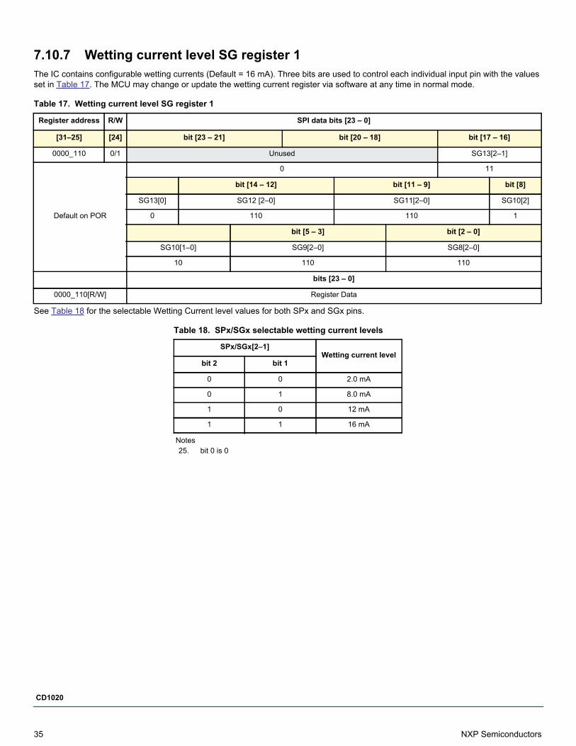
7.10.7 Wetting current level SG register 1The IC contains configurable wetting currents (Default = 16 mA). Three bits are used to control each individual input pin with the values set in Table 17. The MCU may change or update the wetting current register via software at any time in normal mode.
Table 17. Wetting current level SG register 1
Register address R/W SPI data bits [23 – 0]
[31–25] [24] bit [23 – 21] bit [20 – 18] bit [17 – 16]
bit [15] bit [14 – 12] bit [11 – 9] bit [8]
bit [7 – 6] bit [5 – 3] bit [2 – 0]
MISO return word bits [23 – 0]
See Table 18 for the selectable Wetting Current level values for both SPx and SGx pins.
Table 18. SPx/SGx selectable wetting current levels
SPx/SGx[2–1]Wetting current level
bit 2 bit 1
25. bit 0 is 0
0000_110 0/1 Unused SG13[2–1]
Default on POR
0 11
SG13[0] SG12 [2–0] SG11[2–0] SG10[2]
0 110 110 1
SG10[1–0] SG9[2–0] SG8[2–0]
10 110 110
0000_110[R/W] Register Data
0 0 2.0 mA
0 1 8.0 mA
1 0 12 mA
1 1 16 mA
Notes
35 NXP Semiconductors
CD1020
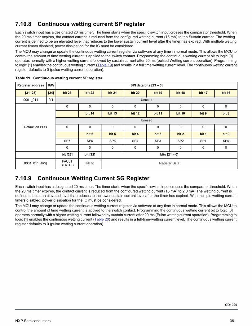
7.10.8 Continuous wetting current SP registerEach switch input has a designated 20 ms timer. The timer starts when the specific switch input crosses the comparator threshold. When the 20 ms timer expires, the contact current is reduced from the configured wetting current (16 mA) to the Sustain current. The wetting current is defined to be an elevated level that reduces to the lower sustain current level after the timer has expired. With multiple wetting current timers disabled, power dissipation for the IC must be considered. The MCU may change or update the continuous wetting current register via software at any time in normal mode. This allows the MCU to control the amount of time wetting current is applied to the switch contact. Programming the continuous wetting current bit to logic [0] operates normally with a higher wetting current followed by sustain current after 20 ms (pulsed Wetting current operation). Programming to logic [1] enables the continuous wetting current (Table 19) and results in a full time wetting current level. The continuous wetting current register defaults to 0 (pulse wetting current operation).
Table 19. Continuous wetting current SP register
Register address R/W SPI data bits [23 – 0]
[31–25] [24] bit 23 bit 22 bit 21 bit 20 bit 19 bit 18 bit 17 bit 16
bit 15 bit 14 bit 13 bit 12 bit 11 bit 10 bit 9 bit 8
bit 7 bit 6 bit 5 bit 4 bit 3 bit 2 bit 1 bit 0
MISO return word bit [23] bit [22] bits [21 – 0]
7.10.9 Continuous Wetting Current SG RegisterEach switch input has a designated 20 ms timer. The timer starts when the specific switch input crosses the comparator threshold. When the 20 ms timer expires, the contact current is reduced from the configured wetting current (16 mA) to 2.0 mA. The wetting current is defined to be at an elevated level that reduces to the lower sustain current level after the timer has expired. With multiple wetting current timers disabled, power dissipation for the IC must be considered. The MCU may change or update the continuous wetting current register via software at any time in normal mode. This allows the MCU to control the amount of time wetting current is applied to the switch contact. Programming the continuous wetting current bit to logic [0] operates normally with a higher wetting current followed by sustain current after 20 ms (Pulse wetting current operation). Programming to logic [1] enables the continuous wetting current (Table 20) and results in a full-time-wetting current level. The continuous wetting current register defaults to 0 (pulse wetting current operation).
0001_011 0/1 Unused
Default on POR
0 0 0 0 0 0 0 0
Unused
0 0 0 0 0 0 0 0
SP7 SP6 SP5 SP4 SP3 SP2 SP1 SP0
0 0 0 0 0 0 0 0
0001_011[R/W] FAULT STATUS INTflg Register Data
NXP Semiconductors 36
CD1020
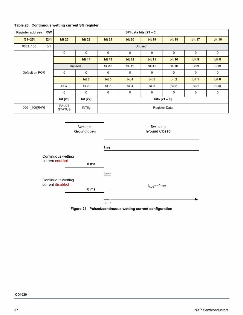
Table 20. Continuous wetting current SG register
Register address R/W SPI data bits [23 – 0]
[31–25] [24] bit 23 bit 22 bit 21 bit 20 bit 19 bit 18 bit 17 bit 16
bit 15 bit 14 bit 13 bit 12 bit 11 bit 10 bit 9 bit 8
bit 7 bit 6 bit 5 bit 4 bit 3 bit 2 bit 1 bit 0
MISO return word bit [23] bit [22] bits [21 – 0]
Figure 21. Pulsed/continuous wetting current configuration
0001_100 0/1 Unused
Default on POR
0 0 0 0 0 0 0 0
Unused SG13 SG12 SG11 SG10 SG9 SG8
0 0 0 0 0 0 0 0
SG7 SG6 SG5 SG4 SG3 SG2 SG1 SG0
0 0 0 0 0 0 0 0
0001_100[R/W] FAULT STATUS INTflg Register Data
37 NXP Semiconductors
CD1020
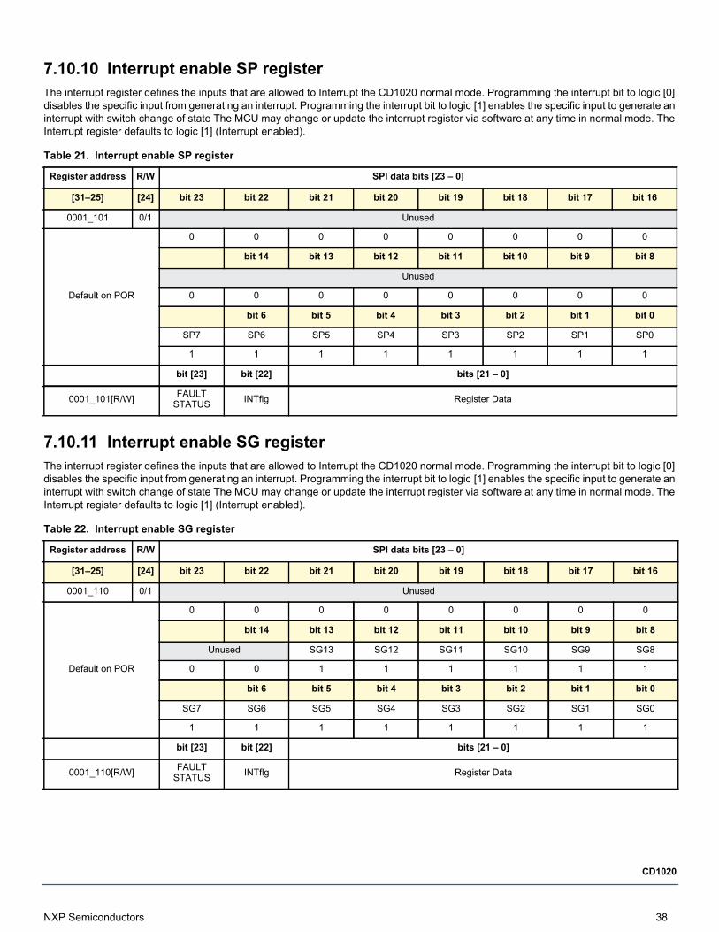
7.10.10 Interrupt enable SP registerThe interrupt register defines the inputs that are allowed to Interrupt the CD1020 normal mode. Programming the interrupt bit to logic [0] disables the specific input from generating an interrupt. Programming the interrupt bit to logic [1] enables the specific input to generate an interrupt with switch change of state The MCU may change or update the interrupt register via software at any time in normal mode. The Interrupt register defaults to logic [1] (Interrupt enabled).
Table 21. Interrupt enable SP register
Register address R/W SPI data bits [23 – 0]
[31–25] [24] bit 23 bit 22 bit 21 bit 20 bit 19 bit 18 bit 17 bit 16
bit 15 bit 14 bit 13 bit 12 bit 11 bit 10 bit 9 bit 8
bit 7 bit 6 bit 5 bit 4 bit 3 bit 2 bit 1 bit 0
MISO return word bit [23] bit [22] bits [21 – 0]
7.10.11 Interrupt enable SG registerThe interrupt register defines the inputs that are allowed to Interrupt the CD1020 normal mode. Programming the interrupt bit to logic [0] disables the specific input from generating an interrupt. Programming the interrupt bit to logic [1] enables the specific input to generate an interrupt with switch change of state The MCU may change or update the interrupt register via software at any time in normal mode. The Interrupt register defaults to logic [1] (Interrupt enabled).
Table 22. Interrupt enable SG register
Register address R/W SPI data bits [23 – 0]
[31–25] [24] bit 23 bit 22 bit 21 bit 20 bit 19 bit 18 bit 17 bit 16
bit 15 bit 14 bit 13 bit 12 bit 11 bit 10 bit 9 bit 8
bit 7 bit 6 bit 5 bit 4 bit 3 bit 2 bit 1 bit 0
MISO return word bit [23] bit [22] bits [21 – 0]
0001_101 0/1 Unused
Default on POR
0 0 0 0 0 0 0 0
Unused
0 0 0 0 0 0 0 0
SP7 SP6 SP5 SP4 SP3 SP2 SP1 SP0
1 1 1 1 1 1 1 1
0001_101[R/W] FAULT STATUS INTflg Register Data
0001_110 0/1 Unused
Default on POR
0 0 0 0 0 0 0 0
Unused SG13 SG12 SG11 SG10 SG9 SG8
0 0 1 1 1 1 1 1
SG7 SG6 SG5 SG4 SG3 SG2 SG1 SG0
1 1 1 1 1 1 1 1
0001_110[R/W] FAULT STATUS INTflg Register Data
NXP Semiconductors 38
CD1020
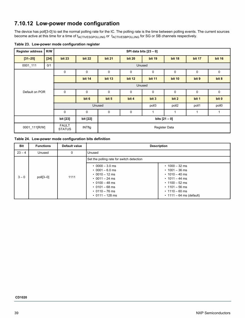
7.10.12 Low-power mode configurationThe device has poll[3-0] to set the normal polling rate for the IC. The polling rate is the time between polling events. The current sources become active at this time for a time of tACTIVESGPOLLING or tACTIVESBPOLLING for SG or SB channels respectively.
Table 23. Low-power mode configuration register
Register address R/W SPI data bits [23 – 0]
[31–25] [24] bit 23 bit 22 bit 21 bit 20 bit 19 bit 18 bit 17 bit 16
bit 15 bit 14 bit 13 bit 12 bit 11 bit 10 bit 9 bit 8
bit 7 bit 6 bit 5 bit 4 bit 3 bit 2 bit 1 bit 0
MISO return word bit [23] bit [22] bits [21 – 0]
Table 24. Low-power mode configuration bits definition
Bit Functions Default value Description
• 0000 – 3.0 ms• 0001 – 6.0 ms• 0010 – 12 ms• 0011 – 24 ms• 0100 – 48 ms• 0101 – 68 ms• 0110 – 76 ms• 0111 – 128 ms
• 1000 – 32 ms• 1001 – 36 ms• 1010 – 40 ms• 1011 – 44 ms• 1100 – 52 ms• 1101 – 56 ms• 1110 – 60 ms• 1111 – 64 ms (default)
0001_111 0/1 Unused
Default on POR
0 0 0 0 0 0 0 0
Unused
0 0 0 0 0 0 0 0
Unused poll3 poll2 poll1 poll0
0 0 0 0 1 1 1 1
0001_111[R/W] FAULT STATUS INTflg Register Data
23 – 4 Unused 0 Unused
3 – 0 poll[3–0] 1111
Set the polling rate for switch detection
39 NXP Semiconductors
CD1020
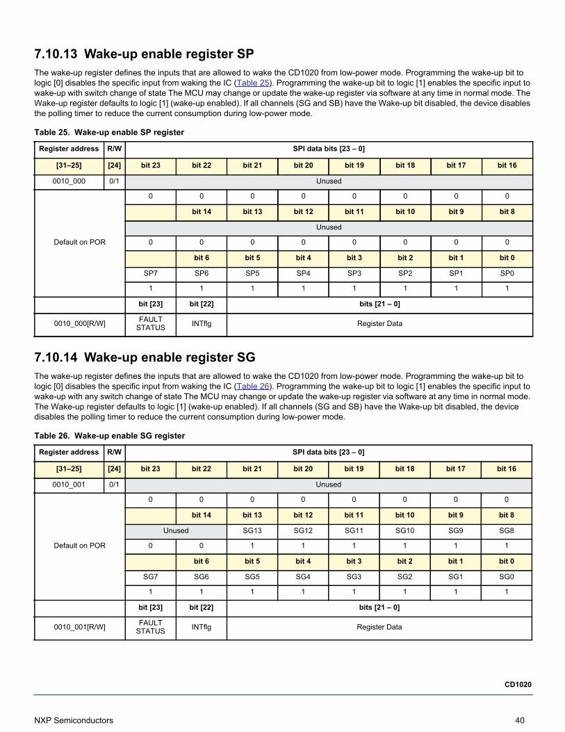
7.10.13 Wake-up enable register SPThe wake-up register defines the inputs that are allowed to wake the CD1020 from low-power mode. Programming the wake-up bit to logic [0] disables the specific input from waking the IC (Table 25). Programming the wake-up bit to logic [1] enables the specific input to wake-up with switch change of state The MCU may change or update the wake-up register via software at any time in normal mode. The Wake-up register defaults to logic [1] (wake-up enabled). If all channels (SG and SB) have the Wake-up bit disabled, the device disables the polling timer to reduce the current consumption during low-power mode.
Table 25. Wake-up enable SP register
Register address R/W SPI data bits [23 – 0]
[31–25] [24] bit 23 bit 22 bit 21 bit 20 bit 19 bit 18 bit 17 bit 16
bit 15 bit 14 bit 13 bit 12 bit 11 bit 10 bit 9 bit 8
bit 7 bit 6 bit 5 bit 4 bit 3 bit 2 bit 1 bit 0
MISO return word bit [23] bit [22] bits [21 – 0]
7.10.14 Wake-up enable register SGThe wake-up register defines the inputs that are allowed to wake the CD1020 from low-power mode. Programming the wake-up bit to logic [0] disables the specific input from waking the IC (Table 26). Programming the wake-up bit to logic [1] enables the specific input to wake-up with any switch change of state The MCU may change or update the wake-up register via software at any time in normal mode. The Wake-up register defaults to logic [1] (wake-up enabled). If all channels (SG and SB) have the Wake-up bit disabled, the device disables the polling timer to reduce the current consumption during low-power mode.
Table 26. Wake-up enable SG register
Register address R/W SPI data bits [23 – 0]
[31–25] [24] bit 23 bit 22 bit 21 bit 20 bit 19 bit 18 bit 17 bit 16
bit 15 bit 14 bit 13 bit 12 bit 11 bit 10 bit 9 bit 8
bit 7 bit 6 bit 5 bit 4 bit 3 bit 2 bit 1 bit 0
MISO return word bit [23] bit [22] bits [21 – 0]
0010_000 0/1 Unused
Default on POR
0 0 0 0 0 0 0 0
Unused
0 0 0 0 0 0 0 0
SP7 SP6 SP5 SP4 SP3 SP2 SP1 SP0
1 1 1 1 1 1 1 1
0010_000[R/W] FAULT STATUS INTflg Register Data
0010_001 0/1 Unused
Default on POR
0 0 0 0 0 0 0 0
Unused SG13 SG12 SG11 SG10 SG9 SG8
0 0 1 1 1 1 1 1
SG7 SG6 SG5 SG4 SG3 SG2 SG1 SG0
1 1 1 1 1 1 1 1
0010_001[R/W] FAULT STATUS INTflg Register Data
NXP Semiconductors 40
CD1020
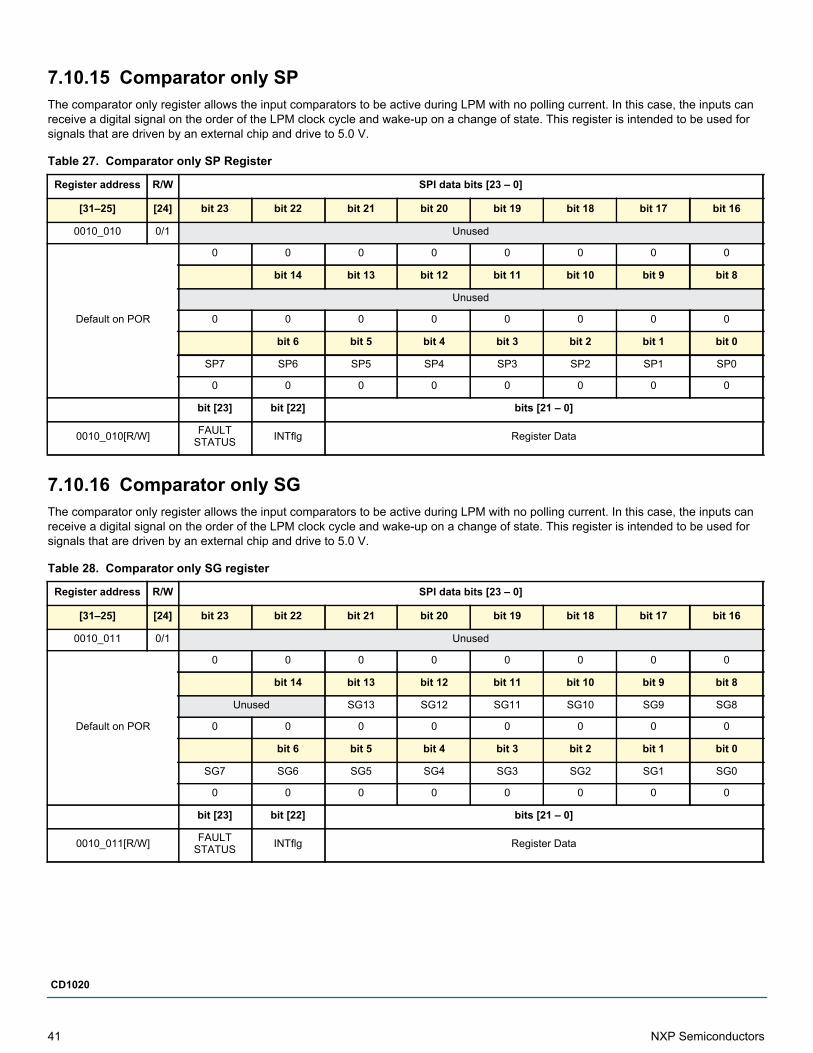
7.10.15 Comparator only SPThe comparator only register allows the input comparators to be active during LPM with no polling current. In this case, the inputs can receive a digital signal on the order of the LPM clock cycle and wake-up on a change of state. This register is intended to be used for signals that are driven by an external chip and drive to 5.0 V.
Table 27. Comparator only SP Register
Register address R/W SPI data bits [23 – 0]
[31–25] [24] bit 23 bit 22 bit 21 bit 20 bit 19 bit 18 bit 17 bit 16
bit 15 bit 14 bit 13 bit 12 bit 11 bit 10 bit 9 bit 8
bit 7 bit 6 bit 5 bit 4 bit 3 bit 2 bit 1 bit 0
MISO return word bit [23] bit [22] bits [21 – 0]
7.10.16 Comparator only SGThe comparator only register allows the input comparators to be active during LPM with no polling current. In this case, the inputs can receive a digital signal on the order of the LPM clock cycle and wake-up on a change of state. This register is intended to be used for signals that are driven by an external chip and drive to 5.0 V.
Table 28. Comparator only SG register
Register address R/W SPI data bits [23 – 0]
[31–25] [24] bit 23 bit 22 bit 21 bit 20 bit 19 bit 18 bit 17 bit 16
bit 15 bit 14 bit 13 bit 12 bit 11 bit 10 bit 9 bit 8
bit 7 bit 6 bit 5 bit 4 bit 3 bit 2 bit 1 bit 0
MISO return word bit [23] bit [22] bits [21 – 0]
0010_010 0/1 Unused
Default on POR
0 0 0 0 0 0 0 0
Unused
0 0 0 0 0 0 0 0
SP7 SP6 SP5 SP4 SP3 SP2 SP1 SP0
0 0 0 0 0 0 0 0
0010_010[R/W] FAULT STATUS INTflg Register Data
0010_011 0/1 Unused
Default on POR
0 0 0 0 0 0 0 0
Unused SG13 SG12 SG11 SG10 SG9 SG8
0 0 0 0 0 0 0 0
SG7 SG6 SG5 SG4 SG3 SG2 SG1 SG0
0 0 0 0 0 0 0 0
0010_011[R/W] FAULT STATUS INTflg Register Data
41 NXP Semiconductors
CD1020
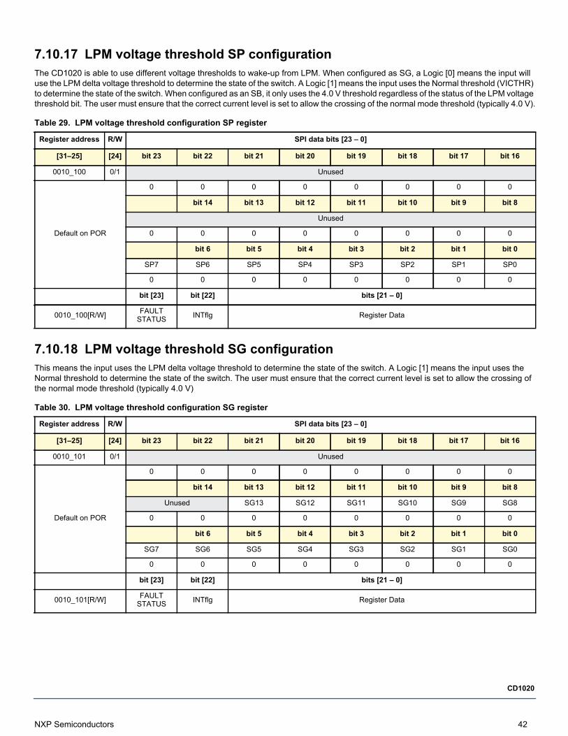
7.10.17 LPM voltage threshold SP configurationThe CD1020 is able to use different voltage thresholds to wake-up from LPM. When configured as SG, a Logic [0] means the input will use the LPM delta voltage threshold to determine the state of the switch. A Logic [1] means the input uses the Normal threshold (VICTHR) to determine the state of the switch. When configured as an SB, it only uses the 4.0 V threshold regardless of the status of the LPM voltage threshold bit. The user must ensure that the correct current level is set to allow the crossing of the normal mode threshold (typically 4.0 V).
Table 29. LPM voltage threshold configuration SP register
Register address R/W SPI data bits [23 – 0]
[31–25] [24] bit 23 bit 22 bit 21 bit 20 bit 19 bit 18 bit 17 bit 16
bit 15 bit 14 bit 13 bit 12 bit 11 bit 10 bit 9 bit 8
bit 7 bit 6 bit 5 bit 4 bit 3 bit 2 bit 1 bit 0
MISO return word bit [23] bit [22] bits [21 – 0]
7.10.18 LPM voltage threshold SG configurationThis means the input uses the LPM delta voltage threshold to determine the state of the switch. A Logic [1] means the input uses the Normal threshold to determine the state of the switch. The user must ensure that the correct current level is set to allow the crossing of the normal mode threshold (typically 4.0 V)
Table 30. LPM voltage threshold configuration SG register
Register address R/W SPI data bits [23 – 0]
[31–25] [24] bit 23 bit 22 bit 21 bit 20 bit 19 bit 18 bit 17 bit 16
bit 15 bit 14 bit 13 bit 12 bit 11 bit 10 bit 9 bit 8
bit 7 bit 6 bit 5 bit 4 bit 3 bit 2 bit 1 bit 0
MISO return word bit [23] bit [22] bits [21 – 0]
0010_100 0/1 Unused
Default on POR
0 0 0 0 0 0 0 0
Unused
0 0 0 0 0 0 0 0
SP7 SP6 SP5 SP4 SP3 SP2 SP1 SP0
0 0 0 0 0 0 0 0
0010_100[R/W] FAULT STATUS INTflg Register Data
0010_101 0/1 Unused
Default on POR
0 0 0 0 0 0 0 0
Unused SG13 SG12 SG11 SG10 SG9 SG8
0 0 0 0 0 0 0 0
SG7 SG6 SG5 SG4 SG3 SG2 SG1 SG0
0 0 0 0 0 0 0 0
0010_101[R/W] FAULT STATUS INTflg Register Data
NXP Semiconductors 42
CD1020
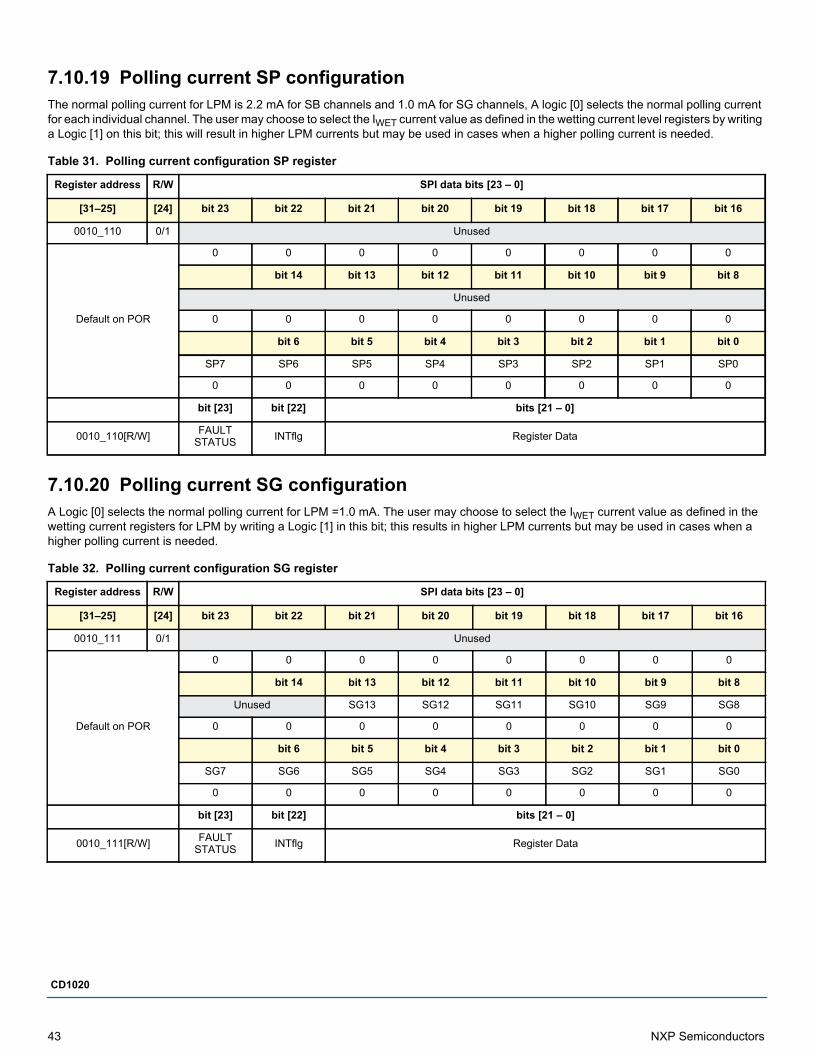
7.10.19 Polling current SP configurationThe normal polling current for LPM is 2.2 mA for SB channels and 1.0 mA for SG channels, A logic [0] selects the normal polling current for each individual channel. The user may choose to select the IWET current value as defined in the wetting current level registers by writing a Logic [1] on this bit; this will result in higher LPM currents but may be used in cases when a higher polling current is needed.
Table 31. Polling current configuration SP register
Register address R/W SPI data bits [23 – 0]
[31–25] [24] bit 23 bit 22 bit 21 bit 20 bit 19 bit 18 bit 17 bit 16
bit 15 bit 14 bit 13 bit 12 bit 11 bit 10 bit 9 bit 8
bit 7 bit 6 bit 5 bit 4 bit 3 bit 2 bit 1 bit 0
MISO return word bit [23] bit [22] bits [21 – 0]
7.10.20 Polling current SG configurationA Logic [0] selects the normal polling current for LPM =1.0 mA. The user may choose to select the IWET current value as defined in the wetting current registers for LPM by writing a Logic [1] in this bit; this results in higher LPM currents but may be used in cases when a higher polling current is needed.
Table 32. Polling current configuration SG register
Register address R/W SPI data bits [23 – 0]
[31–25] [24] bit 23 bit 22 bit 21 bit 20 bit 19 bit 18 bit 17 bit 16
bit 15 bit 14 bit 13 bit 12 bit 11 bit 10 bit 9 bit 8
bit 7 bit 6 bit 5 bit 4 bit 3 bit 2 bit 1 bit 0
MISO return word bit [23] bit [22] bits [21 – 0]
0010_110 0/1 Unused
Default on POR
0 0 0 0 0 0 0 0
Unused
0 0 0 0 0 0 0 0
SP7 SP6 SP5 SP4 SP3 SP2 SP1 SP0
0 0 0 0 0 0 0 0
0010_110[R/W] FAULT STATUS INTflg Register Data
0010_111 0/1 Unused
Default on POR
0 0 0 0 0 0 0 0
Unused SG13 SG12 SG11 SG10 SG9 SG8
0 0 0 0 0 0 0 0
SG7 SG6 SG5 SG4 SG3 SG2 SG1 SG0
0 0 0 0 0 0 0 0
0010_111[R/W] FAULT STATUS INTflg Register Data
43 NXP Semiconductors
CD1020
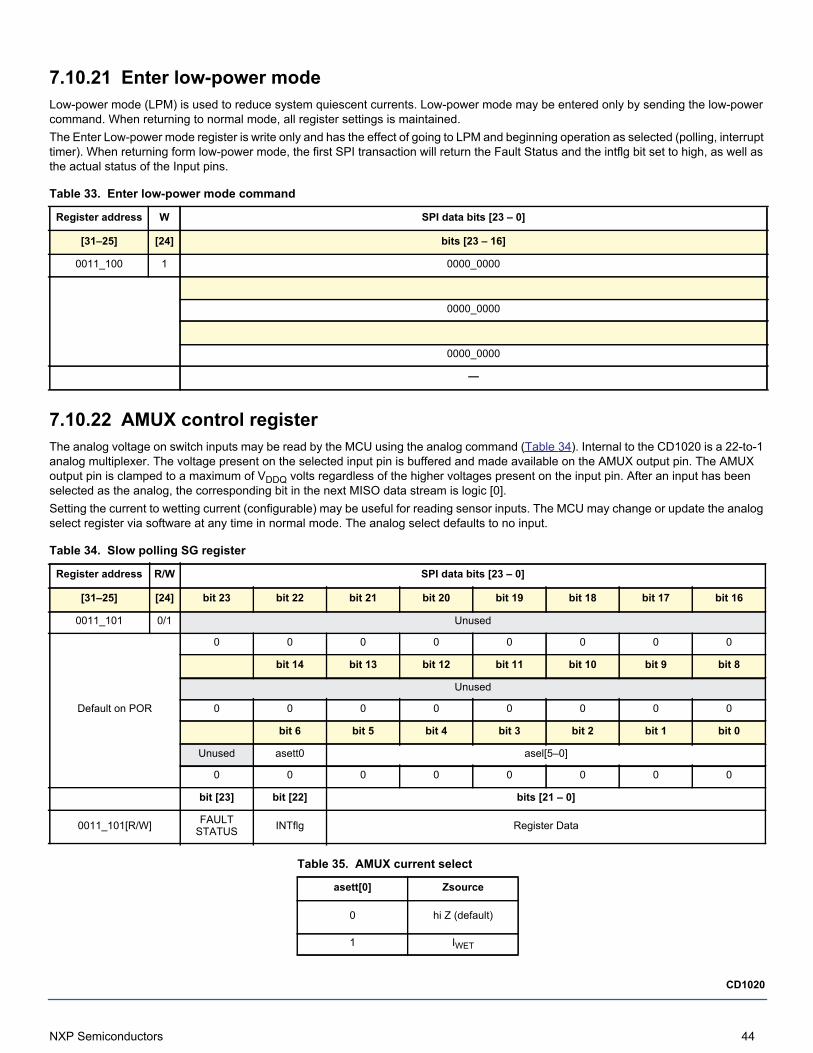
7.10.21 Enter low-power modeLow-power mode (LPM) is used to reduce system quiescent currents. Low-power mode may be entered only by sending the low-power command. When returning to normal mode, all register settings is maintained.The Enter Low-power mode register is write only and has the effect of going to LPM and beginning operation as selected (polling, interrupt timer). When returning form low-power mode, the first SPI transaction will return the Fault Status and the intflg bit set to high, as well as the actual status of the Input pins.
Table 33. Enter low-power mode command
Register address W SPI data bits [23 – 0]
[31–25] [24] bits [23 – 16]
bits [15 – 8]
bits [7 – 0]
MISO return word —
7.10.22 AMUX control registerThe analog voltage on switch inputs may be read by the MCU using the analog command (Table 34). Internal to the CD1020 is a 22-to-1 analog multiplexer. The voltage present on the selected input pin is buffered and made available on the AMUX output pin. The AMUX output pin is clamped to a maximum of VDDQ volts regardless of the higher voltages present on the input pin. After an input has been selected as the analog, the corresponding bit in the next MISO data stream is logic [0]. Setting the current to wetting current (configurable) may be useful for reading sensor inputs. The MCU may change or update the analog select register via software at any time in normal mode. The analog select defaults to no input.
Table 34. Slow polling SG register
Register address R/W SPI data bits [23 – 0]
[31–25] [24] bit 23 bit 22 bit 21 bit 20 bit 19 bit 18 bit 17 bit 16
bit 15 bit 14 bit 13 bit 12 bit 11 bit 10 bit 9 bit 8
bit 7 bit 6 bit 5 bit 4 bit 3 bit 2 bit 1 bit 0
MISO return word bit [23] bit [22] bits [21 – 0]
Table 35. AMUX current select
asett[0] Zsource
0011_100 1 0000_0000
0000_0000
0000_0000
0011_101 0/1 Unused
Default on POR
0 0 0 0 0 0 0 0
Unused
0 0 0 0 0 0 0 0
Unused asett0 asel[5–0]
0 0 0 0 0 0 0 0
0011_101[R/W] FAULT STATUS INTflg Register Data
0 hi Z (default)
1 IWET
NXP Semiconductors 44
CD1020
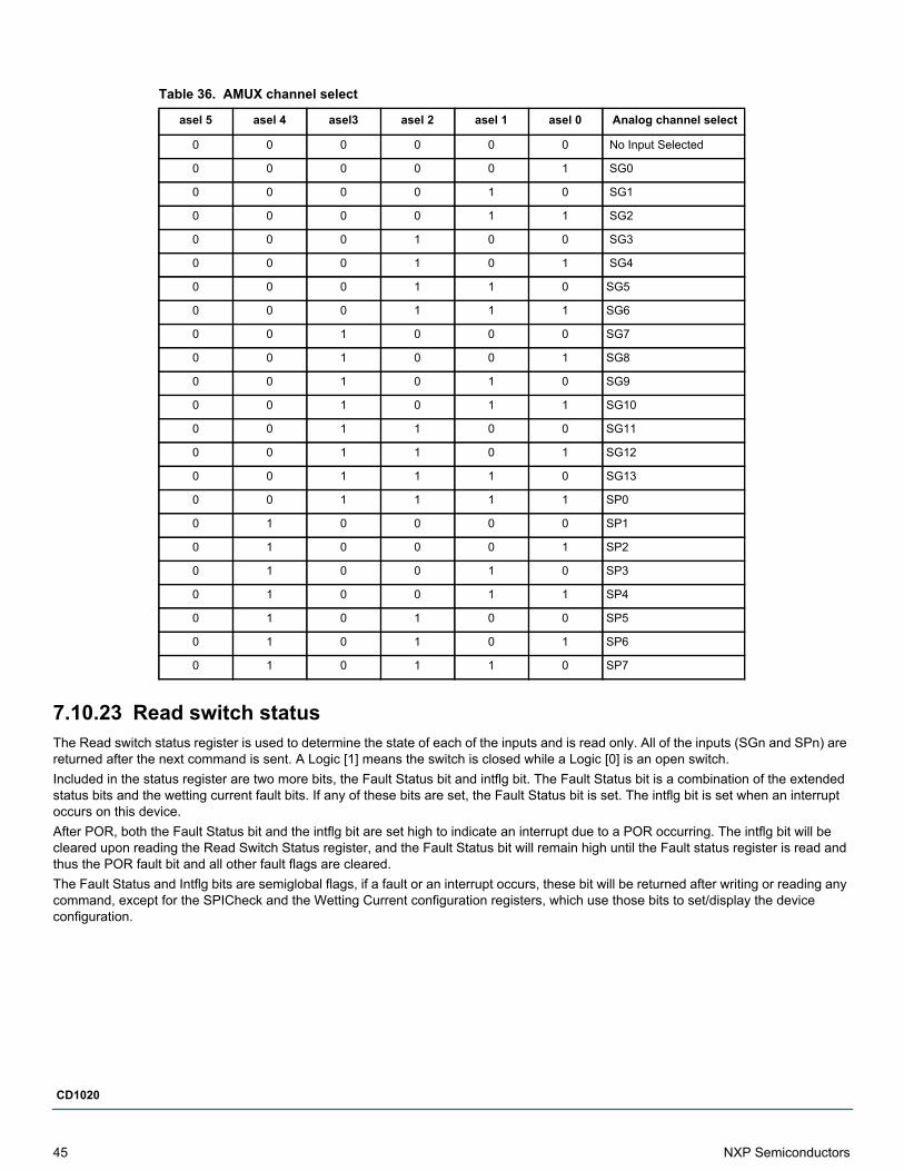
Table 36. AMUX channel select
asel 5 asel 4 asel3 asel 2 asel 1 asel 0 Analog channel select
7.10.23 Read switch statusThe Read switch status register is used to determine the state of each of the inputs and is read only. All of the inputs (SGn and SPn) are returned after the next command is sent. A Logic [1] means the switch is closed while a Logic [0] is an open switch. Included in the status register are two more bits, the Fault Status bit and intflg bit. The Fault Status bit is a combination of the extended status bits and the wetting current fault bits. If any of these bits are set, the Fault Status bit is set. The intflg bit is set when an interrupt occurs on this device.After POR, both the Fault Status bit and the intflg bit are set high to indicate an interrupt due to a POR occurring. The intflg bit will be cleared upon reading the Read Switch Status register, and the Fault Status bit will remain high until the Fault status register is read and thus the POR fault bit and all other fault flags are cleared.The Fault Status and Intflg bits are semiglobal flags, if a fault or an interrupt occurs, these bit will be returned after writing or reading any command, except for the SPICheck and the Wetting Current configuration registers, which use those bits to set/display the device configuration.
0 0 0 0 0 0 No Input Selected
0 0 0 0 0 1 SG0
0 0 0 0 1 0 SG1
0 0 0 0 1 1 SG2
0 0 0 1 0 0 SG3
0 0 0 1 0 1 SG4
0 0 0 1 1 0 SG5
0 0 0 1 1 1 SG6
0 0 1 0 0 0 SG7
0 0 1 0 0 1 SG8
0 0 1 0 1 0 SG9
0 0 1 0 1 1 SG10
0 0 1 1 0 0 SG11
0 0 1 1 0 1 SG12
0 0 1 1 1 0 SG13
0 0 1 1 1 1 SP0
0 1 0 0 0 0 SP1
0 1 0 0 0 1 SP2
0 1 0 0 1 0 SP3
0 1 0 0 1 1 SP4
0 1 0 1 0 0 SP5
0 1 0 1 0 1 SP6
0 1 0 1 1 0 SP7
45 NXP Semiconductors
CD1020
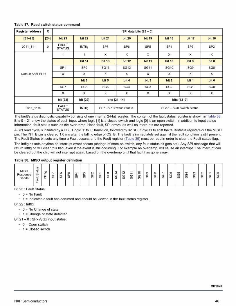
Table 37. Read switch status command
Register address R SPI data bits [23 – 0]
[31–25] [24] bit 23 bit 22 bit 21 bit 20 bit 19 bit 18 bit 17 bit 16
bit 15 bit 14 bit 13 bit 12 bit 11 bit 10 bit 9 bit 8
bit 7 bit 6 bit 5 bit 4 bit 3 bit 2 bit 1 bit 0
MISO return word bit [23] bit [22] bits [21–14] bits [13–0]
0011_1110
The fault/status diagnostic capability consists of one internal 24-bit register. The content of the fault/status register is shown in Table 38. Bits 0 – 21 show the status of each input where logic [1] is a closed switch and logic [0] is an open switch. In addition to input status information, fault status such as die over-temp, Hash fault, SPI errors, as well as interrupts are reported.A SPI read cycle is initiated by a CS_B logic ‘1’ to ‘0’ transition, followed by 32 SCLK cycles to shift the fault/status registers out the MISO pin. The INT_B pin is cleared 1.0 ms after the falling edge of CS_B. The fault is immediately set again if the fault condition is still present. The Fault Status bit sets any time a Fault occurs, and the Fault register (Table 39) must be read in order to clear the Fault status flag. The intflg bit sets anytime an interrupt event occurs (change of state on switch, any fault status bit gets set). Any SPI message that will return intflg bit will clear this flag, even if the event is still occurring. For example an overtemp, will cause an interrupt. The interrupt can be cleared but the chip will not interrupt again, based on the overtemp until that fault has gone away.
Table 38. MISO output register definition
Bit 23 : Fault Status:• 0 = No Fault • 1 = Indicates a fault has occurred and should be viewed in the fault status register.
Bit 22 : Intflg: • 0 = No Change of state• 1 = Change of state detected.
Bit 21 – 0 : SPx /SGx input status:• 0 = Open switch• 1 = Closed switch
0011_111 0 FAULT STATUS INTflg SP7 SP6 SP5 SP4 SP3 SP2
Default After POR
1 1 X X X X X X
SP1 SP0 SG13 SG12 SG11 SG10 SG9 SG8
X X X X X X X X
SG7 SG6 SG5 SG4 SG3 SG2 SG1 SG0
X X X X X X X X
FAULT STATUS INTflg SP7 –SP0 Switch Status SG13 – SG0 Switch Status
MISO Response
Sends
Faul
t Sta
tus
INTf
lg
SP7
SP6
SP5
SP4
SP3
SP2
SP1
SP0
SG13
SG12
SG11
SG10
SG9
SG8
SG7
SG6
SG5
SG4
SG3
SG2
SG1
SG0
NXP Semiconductors 46
CD1020
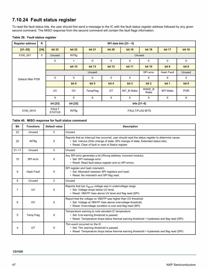
7.10.24 Fault status registerTo read the fault status bits, the user should first send a message to the IC with the fault status register address followed by any given second command. The MISO response from the second command will contain the fault flags information.
Table 39. Fault status register
Register address R SPI data bits [23 – 0]
[31–25] [24] bit 23 bit 22 bit 21 bit 20 bit 19 bit 18 bit 17 bit 16
bit 15 bit 14 bit 13 bit 12 bit 11 bit 10 bit 9 bit 8
bit 7 bit 6 bit 5 bit 4 bit 3 bit 2 bit 1 bit 0
MISO return word bit [23] bit [22] bits [21–0]
0100_0010
0100_001 0 Unused INTflg Unused
Default After POR
0 1 0 0 0 0 0 0
Unused SPI error Hash Fault Unused
0 0 0 0 0 X X 0
UV OV TempFlag OT INT_B Wake WAKE_B Wake SPI Wake POR
X X X X X X X X
FAULT STATUS INTflg FAULT/FLAG BITS
Table 40. MISO response for fault status command
Bit Functions Default value Description
23 Unused 0 Unused
22 INTflg XReports that an Interrupt has occurred, user should read the status register to determine cause.
• Set: Various (SGx change of state, SPx change of state, Extended status bits). • Reset: Clear of fault or read of Status register
21–11 Unused 0 Unused
10 SPI error XAny SPI error generates a bit (Wrong address, incorrect modulo).
• Set: SPI message error. • Reset: Read fault status register and no SPI errors.
9 Hash Fault XSPI register and hash mismatch.
• Set: Mismatch between SPI registers and hash. • Reset: No mismatch and SPI flag read.
8 Unused 0 Unused
7 UV XReports that low VBATP voltage was in undervoltage range
• Set: Voltage drops below UV level. • Reset: VBATP rises above UV level and flag read (SPI)
6 OV XReport that the voltage on VBATP was higher than OV threshold
• Set: Voltage at VBATP rises above overvoltage threshold. • Reset: Overvoltage condition is over and flag read (SPI)
5 Temp Flag XTemperature warning to note elevated IC temperature
• Set: tLIM warning threshold is passed. • Reset: Temperature drops below thermal warning threshold + hysteresis and flag read (SPI)
4 OT XTlim event occurred on the IC
• Set: Tlim warning threshold is passed. • Reset: Temperature drops below thermal warning threshold + hysteresis and flag read (SPI)
47 NXP Semiconductors
CD1020
7.10.25 Interrupt requestThe MCU may request an Interrupt pulse of duration 100 s by sending the Interrupt request command. After an Interrupt request command, the CD1020 returns the Interrupt request command word, as well as the Fault status and INTflg bits set if a fault/interrupt event occurred. Sending an interrupt request command does not set the INTflg bit itself.
Table 41. Interrupt request command
Register address W SPI data bits [23 – 0]
[31–25] [24] bits [23 – 16]
bits [15 – 8]
bits [7 – 0]
MISO return word bit [23] bit [22] bits [21–0]
0100_0111
7.10.26 Reset registerWriting to this register causes all of the SPI registers to reset.
Table 42. Reset command
Register address W SPI data bits [23 – 0]
[31–25] [24] bits [23 – 16]
bits [15 – 8]
bits [7 – 0]
MISO return word bit [23] bit [22] bits [21–0]
0011_1110
3 INT_B Wake XPart awakens via an external INT_B falling edge
• Set: INT_B Wakes the part from LPM (external falling edge) • Reset: flag read (SPI).
2 WAKE_B Wake XPart awakens via an external WAKE_B falling edge
• Set: External WAKE_B falling edge seen • Reset: flag read (SPI).
1 SPI Wake XPart awaken via a SPI message
• Set: SPI message wakes the IC from LPM • Reset: flag read (SPI).
0 POR XReports a POR event occurred.
• Set: Voltage at VBATP pin dropped below VBATP(POR) voltage • Reset: flag read (SPI)
0100_011 1 0000_0000
0000_0000
0000_0000
FAULT STATUS INTflg 0
0100_100 1 0000_0000
0000_0000
0000_0000
FAULT STATUS INTflg Switch Status
Table 40. MISO response for fault status command (continued)
NXP Semiconductors 48
CD1020
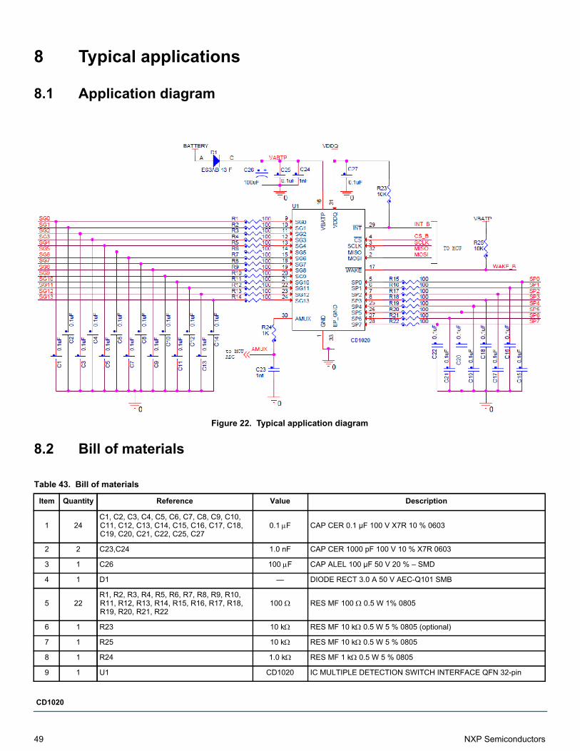
8 Typical applications
8.1 Application diagram
Figure 22. Typical application diagram
8.2 Bill of materials
Table 43. Bill of materials
Item Quantity Reference Value Description
1 24C1, C2, C3, C4, C5, C6, C7, C8, C9, C10, C11, C12, C13, C14, C15, C16, C17, C18, C19, C20, C21, C22, C25, C27
0.1F CAP CER 0.1 μF 100 V X7R 10 % 0603
2 2 C23,C24 1.0 nF CAP CER 1000 pF 100 V 10 % X7R 0603
3 1 C26 100 F CAP ALEL 100 μF 50 V 20 % – SMD
4 1 D1 — DIODE RECT 3.0 A 50 V AEC-Q101 SMB
5 22R1, R2, R3, R4, R5, R6, R7, R8, R9, R10, R11, R12, R13, R14, R15, R16, R17, R18, R19, R20, R21, R22
100 RES MF 100 0.5 W 1% 0805
6 1 R23 10 k RES MF 10 k 0.5 W 5 % 0805 (optional)
7 1 R25 10 k RES MF 10 k 0.5 W 5 % 0805
8 1 R24 1.0 k RES MF 1 k 0.5 W 5 % 0805
9 1 U1 CD1020 IC MULTIPLE DETECTION SWITCH INTERFACE QFN 32-pin
49 NXP Semiconductors
CD1020
8.3 Abnormal operation The CD1020 could be subject to various conditions considered abnormal as defined within this section.
8.3.1 Reverse batteryThis device with applicable external components will not be damaged by exposure to reverse battery conditions of –14 V. This test is performed for a period of one minute at 25 °C. In addition, this negative voltage condition does not force any of the logic level I/O pins to a negative voltage less than –0.6 V at 10 mA or to a positive voltage greater the 5.0 V. This ensures protection of the digital device interfacing with this device.
8.3.2 Ground offsetThe applicable driver outputs and/or current sense inputs are capable of operation with a ground offset of 1.0 V. The device will not be damaged by exposure to this condition and will maintain specified functionality. AMUX output voltage deviates when there are negative ground offsets on other SGx/SPx pins.
8.3.3 Shorts to groundAll I/Os of the device that are available at the module connector are protected against shorts to ground with maximum ground offset considered, i.e. –1.0 V referenced to device ground or other application specific value. The device will not be damaged by this condition.
8.3.4 Shorts to batteryAll I/Os of the device that are available at the module connector are protected against a short to battery (voltage value is application dependent, there may be cases where short to jump start or load dump voltage values are required). The device will not be damaged by this condition.
8.3.5 Unpowered shorts to batteryAll I/Os of the device that are available at the module connector are protected against unpowered (battery to the module is open) shorts to battery per application specifics. The device will not be damaged by this condition, will not enable any outputs nor backfeed onto the power rails (VBATP, VDDQ) or the digital I/O pins.
8.3.6 Loss of module groundThe definition of a loss of ground condition at the device level is that all pins of the IC detects very low impedance-to-battery. The nomenclature is suited to a test environment. In the application, a loss of ground condition results in all I/O pins floating to battery voltage, while all externally referenced I/O pins are, at worst case, pulled to ground. All applicable driver outputs and current sense inputs are protected against excessive leakage current due to loads that are referenced to an external ground (high-side drivers).
8.3.7 Loss of module batteryThe loss of battery condition at the parts level is that the power input pins of the IC see infinite impedance to the battery supply voltage (depending upon the application) but there is some undefined impedance looking from these pins to ground. All applicable driver outputs and current sense inputs are protected against excessive leakage current due to loads that are referenced to an external battery connection (low-side drivers).
NXP Semiconductors 50
CD1020
9 Packaging
9.1 Package mechanical dimensionsPackage dimensions are provided in package drawings. To find the most current package outline drawing, go to www.nxp.com and perform a keyword search for the drawing’s document number.
Table 44. Packaging information
Package Suffix Package outline drawing number
32-pin QFN (WF-type) ES 98ASA00656D
51 NXP Semiconductors
CD1020
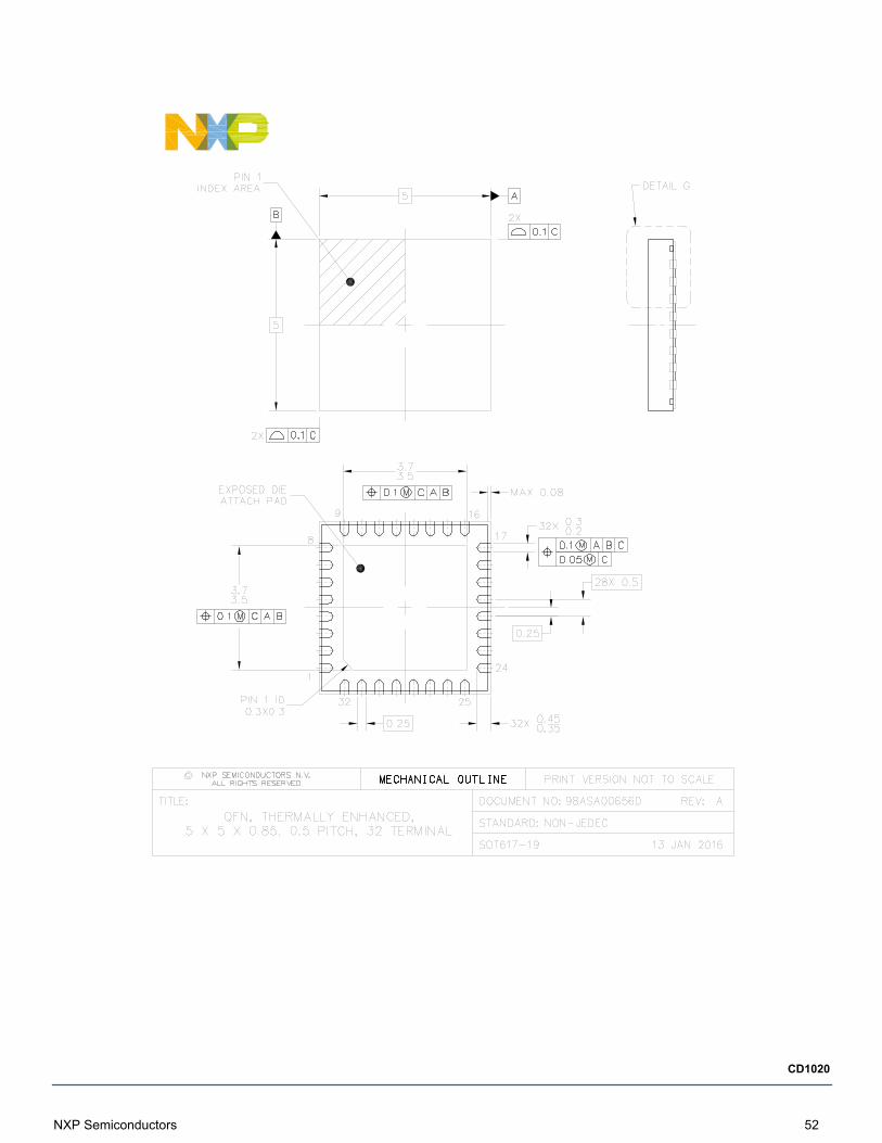
NXP Semiconductors 52
CD1020
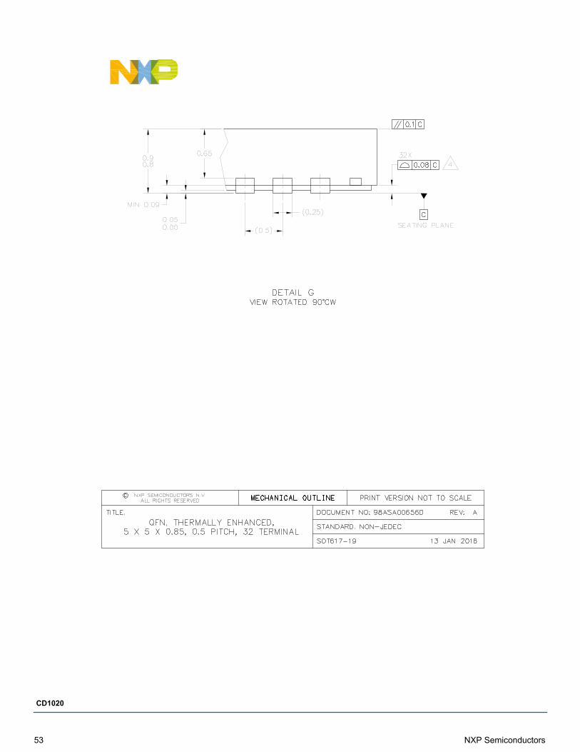
53 NXP Semiconductors
CD1020
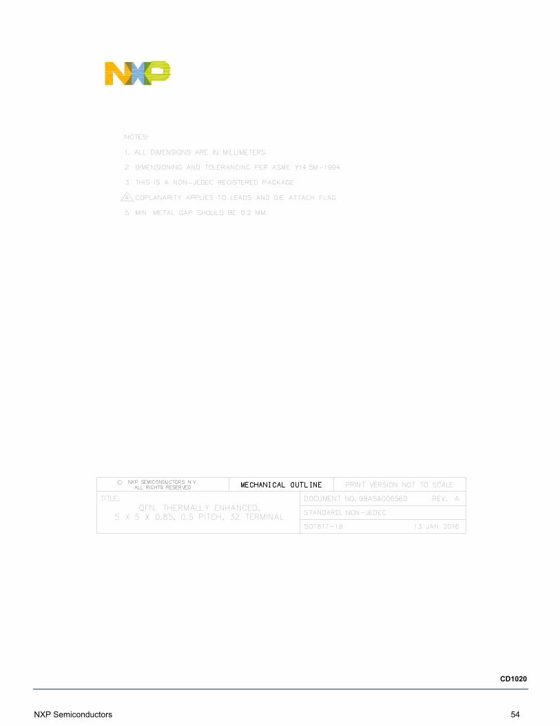
NXP Semiconductors 54
CD1020
Table 45. CD1020 reference documents
Reference Description
Revision Date Description of changes
• Initial release
• Changed document specification state from Product Preview to Advance Information• Table 3, Maximum ratings
• Deleted VESD6-1, description, parameter, and footnote 5
• Table 6, Static electrical characteristics• Added footnote ‘AMUX output voltage deviates when there are negative inputs on other SGx/SPx pins.’ to
VGNDOFFSET and VOFFSET
• Table 7, Dynamic electrical characteristics• Deleted iINT-TIMER row
• Section 7.8, deleted last sentence of section, ‘Since the device is required...’• Table 11, Device configuration register
• Changed bit 9 from Aconfig1 to Unused• Changed bit 8 from Aconfig0 to Unused
• Section 7.10.22, AMUX control register• Changed ‘Internal to the CD1020 is a 24-to-1...’ to ‘Internal to the CD1020 is a 22-to-1...’
• Section 8.2, Bill of materials• Changed item 9 from ‘...SWITCH INTERFACE SOIC32’ to ‘...SWITCH INTERFACE QFN 32 pin’
10 Reference section
11 Revision history
CDF-AEC-Q100 Stress Test Qualification For Automotive Grade Integrated Circuits
Q-1000 Qualification Specification for Integrated Circuits
SQ-1001 Specification Conformance
ISO 7637 Electrical Disturbances from Conduction and Coupling
ISO 61000 Electromagnetic Compatibility
1.0 6/2017
2.0 2/2018
55 NXP Semiconductors
CD1020
Information in this document is provided solely to enable system and software implementers to use NXP products.
There are no expressed or implied copyright licenses granted hereunder to design or fabricate any integrated circuits
based on the information in this document. NXP reserves the right to make changes without further notice to any
products herein.
NXP makes no warranty, representation, or guarantee regarding the suitability of its products for any particular
purpose, nor does NXP assume any liability arising out of the application or use of any product or circuit, and
specifically disclaims any and all liability, including without limitation, consequential or incidental damages. "Typical"
parameters that may be provided in NXP data sheets and/or specifications can and do vary in different applications,
and actual performance may vary over time. All operating parameters, including "typicals," must be validated for each
customer application by the customer's technical experts. NXP does not convey any license under its patent rights nor
the rights of others. NXP sells products pursuant to standard terms and conditions of sale, which can be found at the
following address:
http://www.nxp.com/terms-of-use.html.
How to Reach Us:Home Page: NXP.com Web Support: http://www.nxp.com/support
NXP, the NXP logo, Freescale, the Freescale logo and SMARTMOS are trademarks of NXP Semiconductors B.V.
All other product or service names are the property of their respective owners. All rights reserved.
© NXP B.V. 2018
Document Number: CD1020Rev. 2.0
2/2018