Embed Size (px)
Citation preview
Novel Low Temperature Processing for Enhanced Properties of
Ion Implanted Thin Films and Amorphous Mixed Oxide Thin Film Transistors
by
Rajitha Vemuri
A Dissertation Presented in Partial Fulfillment of the Requirements for the Degree
Doctor of Philosophy
Approved April 2013 by the Graduate Supervisory Committee:
Terry L Alford, Chair N David Theodore
Michael Goryll
ARIZONA STATE UNIVERSITY
May 2013

©2013 Rajitha Neeha Priyanka Vemuri All Rights Reserved
i
ABSTRACT
This research emphasizes the use of low energy and low temperature post
processing to improve the performance and lifetime of thin films and thin film
transistors, by applying the fundamentals of interaction of materials with
conductive heating and electromagnetic radiation. Single frequency microwave
anneal is used to rapidly recrystallize the damage induced during ion
implantation in Si substrates. Volumetric heating of the sample in the presence of
the microwave field facilitates quick absorption of radiation to promote
recrystallization at the amorphous-crystalline interface, apart from electrical
activation of the dopants due to relocation to the substitutional sites. Structural
and electrical characterization confirm recrystallization of heavily implanted Si
within 40 seconds anneal time with minimum dopant diffusion compared to rapid
thermal annealed samples. The use of microwave anneal to improve
performance of multilayer thin film devices, e.g. thin film transistors (TFTs)
requires extensive study of interaction of individual layers with electromagnetic
radiation.
This issue has been addressed by developing detail understanding of thin
films and interfaces in TFTs by studying reliability and failure mechanisms upon
extensive stress test. Electrical and ambient stresses such as illumination,
thermal, and mechanical stresses are inflicted on the mixed oxide based thin film
transistors, which are explored due to high mobilities of the mixed oxide (indium
zinc oxide, indium gallium zinc oxide) channel layer material. Semiconductor
ii
parameter analyzer is employed to extract transfer characteristics, useful to
derive mobility, subthreshold, and threshold voltage parameters of the
transistors. Low temperature post processing anneals compatible with polymer
substrates are performed in several ambients (oxygen, forming gas and vacuum)
at 150 °C as a preliminary step. The analysis of th e results pre and post low
temperature anneals using device physics fundamentals assists in categorizing
defects leading to failure/degradation as: oxygen vacancies, thermally activated
defects within the bandgap, channel-dielectric interface defects, and acceptor-
like or donor-like trap states. Microwave anneal has been confirmed to enhance
the quality of thin films, however future work entails extending the use of
electromagnetic radiation in controlled ambient to facilitate quick post fabrication
anneal to improve the functionality and lifetime of these low temperature
fabricated TFTs.

iii
DEDICATION
To my parents Lakshmi and Shashi, who have loved and supported me through
all my unconventional decisions, my sister Malini who makes me want to be a
better person, my grandparents who brought me up and cared for me like
parents, and my in-laws who feel a sense of pride and joy for my success, just as
they do for their son’s achievements.
To my eternal best friend & husband Shantanu, and my closest friend over the
decades Divya Paruchuri, for being the truest friends, for correcting me when I
was wrong, for guiding me when I was distracted, and for always reminding me
that I am capable of being better than what others think of me.
iv
ACKNOWLEDGMENTS
I am greatly indebted to Dr. Terry Alford for his continual support and
guidance throughout my graduate study, and the trust he placed in me. I can’t
thank enough students from Dr. Alford’s group: Anil Indluru, Aritra Dhar, Chia-
Ling Fang, Hyung Woo Choi, Joe Carptenter III, Karthik Sivaramakrishnan,
Mandar Gadre, Muhammad Ruhul Hasin, Pai Liu, Sayantan Das, Sebastian
Husein, Shengke Zhang, Zhao Zhao, and Andrew Knight, for their inspiration and
support, not to forget the great times we spent as a group. I express my gratitude
to Dr. David Theodore and Dr. Michael Goryll for being my committee members,
and taking the time and interest for evaluating my work. I am extremely grateful
to Late Ms. Yolanda Murphy, the department academic advisor, who was always
around to help me, and to Late Prof. Dieter K. Schroder whose way of life,
dedication to science and humble demeanor will serve as a life lesson to me.
I thank my friends and well-wishers from Hyderabad and Tempe for their
support, positive criticism and for being a part of my life, and most of all the good
times during these years at ASU. My heartfelt gratitude to Pastor Sanghoon Yoo
and Mrs. Yoo-Kyung Yoo, who played an undeniable role in reviving my
personality, and encouraged me to make decisions leading me through this path.
I acknowledge the support of National Science Foundation (C. Ying, Grant
No. DMR-0602716) who partially funded this research, and the staff at Flexible
Display Center at ASU Research Park for providing wafers crucial for this work.
v
TABLE OF CONTENTS
Page
LIST OF TABLES ................................................................................................... viii
LIST OF FIGURES ................................................................................................... ix
CHAPTER
1 INTRODUCTION .................................................................................... 1
1.1 Ion Implantation ........................................................................ 1
1.1.a Damage ........................................................................ 1
1.1.b Complications ............................................................... 3
1.1.c Thin films and shallow depth transistors ....................... 4
1.1.d Microwaves technology and loss mechanisms ............ 6
1.1.e High Z materials ............................................................ 9
1.2 Metal oxide based thin film transistors ................................... 10
1.3 Summary ................................................................................ 11
2 EXPERIMENTAL PROCEDURE .......................................................... 13
2.1 Sample preparation ................................................................ 13
2.2 Material Characterization ....................................................... 15
2.2.a Raman Spectroscopy ................................................. 15
2.2.b Rutherford Backscattering Spectrometry .................... 17
2.2.c Sheet Resistance measurement ................................ 19
2.2.d Hall measurements ..................................................... 21
2.2.e Cross-section Transmission Electron Microscopy and
Focussed Ion Beam Milling ......................................... 25
vi
CHAPTER Page
2.2.f Secondary Ion Mass Spectroscopy ............................ 27
2.3 Device Characterization (Thin Film Transistor Analysis) ....... 29
3 DOPANT ACTIVATION AND DIFFUSION PROFILE OF As
IMPLANTED Si ................................................................................ 31
3.1 Introduction ............................................................................ 31
3.2 Experimental Procedure ........................................................ 32
3.3 Results ................................................................................... 34
3.4 Discussion .............................................................................. 41
3.5 Conclusion ............................................................................. 45
4 RECRYSTALLIZATION OF As AND as-IMPLANTED Si ..................... 46
4.1 Introduction ............................................................................ 46
4.2 Structural Characterization .................................................... 49
4.3 Results ................................................................................... 51
4.4 Discussion .............................................................................. 55
4.5 Conclusion ............................................................................. 57
5 KINETIC STRESS TESTING AND INFLUENCE OF LONG TIME
ANNEALS ON THE BEHAVIOR OF IZO TFTs ............................... 58
5.1 Introduction ............................................................................ 58
5.2 Experimental Details .............................................................. 60
5.3 Results and Discussion .......................................................... 61
5.4 Conclusion ............................................................................. 76
5.5 Appendix ................................................................................ 77
vii
CHAPTER Page
6 INVESTIGATION OF DEFECT GENERATION AND ANNIHILATION
IN IGZO TFTs DURING PRACTICAL STRESS CONDITIONS:
ILLUMINATION AND ELECTRICAL BIAS ...................................... 79
6.1 Introduction ............................................................................ 79
6.2 Experimental Procedure ........................................................ 80
6.3 Results ................................................................................... 83
6.4 Discussion .............................................................................. 90
6.5 Conclusion ............................................................................. 97
7 SUMMARY ........................................................................................... 99
7.1 Introduction ............................................................................ 99
7.2 Materials Characterization ................................................... 100
7.3 Dopant Activation and Dopant Diffusion of As IMPLANTED Si
............................................................................................. 101
7.4 Recrystallization of As Implanted Si and as Implanted Si ... 102
7.5 Kinetic Stress Testing and Influence of Long Time Anneals on
Behavior of IZO TFTs .......................................................... 103
7.6 Investigation of Defect Generation and Annihilation in IGZO
TFTs During Practical Stress Conditions: Illumination and
Electrical Bias ....................................................................... 104
7.7 Conclusion ........................................................................... 105
7.8 Future Work ......................................................................... 107
REFERENCES ..................................................................................................... 108
viii
LIST OF TABLES
Table Page
1. Sheet Resistance measurements vs Anneal times .......................... 35
2. Hall measurements of A: 30 keV 1×10¹⁵ As+ cm-2 and B: 180 keV
1×10¹⁵ As+ cm-2 implanted Si ........................................................... 37
ix
LIST OF FIGURES
Figure Page
1.1. Frequency dependence of the several contributions to the
polarizability schematic ....................................................................... 8
2.1. a) The microwave pyrometer-susceptor setup; b) pyrometer to
measure in-situ temperature; c) SiC-Al susceptor with a 1.5 cm × 1.5
cm groove to mount the sample to provide uniform heating ............ 14
2.2. Raman Spectrometer used to examine crystalline structure of the
samples ............................................................................................. 16
2.3. Schematic of a typical Rutherford backscattering system. A General
Ionex 1.7 MV Tandetron accelerator was used for RBS at ASU ...... 18
2.4. Layout of atypical four-point probe setup. Measurements taken at
ASU had a probe spacing of 2 mm. Where S = spacing between the
probes, and t = thickness of the sample ........................................... 20
2.5. Sample labeling for the contacts made to perform Van der Pauw Hall
measurements ................................................................................... 22
2.6. Ecopia HMS-3000 Hall Effect Measurement System used at ASU .. 25
2.7. FEI 835 focused-ion beam tool with a Ga ion-source ....................... 26
2.8. Philips CM200 FEG TEM used at ASU ............................................ 27
2.9. Mechanism of SIMS analyzer ............................................................ 28
2.10. Mechanism of SIMS analyzer ............................................................ 29
3.1. Temperature vs Time profile of As implanted Si with and without
Susceptor .......................................................................................... 35
x
Figure Page
3.2. Ion channeling results of As+ implanted Si ........................................ 37
3.3. Sheet Resistance measurements of the different dosage and
implantation energy As implanted Si at different anneal times ........ 39
3.4. SIMS profile of 180 keV 1×10¹⁵ As+ impanted Si annealed under
different conditions ............................................................................ 41
4.1. Temperature vs time profile of As implanted Si and as-implanted Si
without a susceptor ............................................................................ 47
4.2. Temperature vs time profile of As implanted Si and as-implanted Si
witht a susceptor ................................................................................ 48
4.3. Raman Spectra of 30 keV 1×1015 cm-2 As implanted Si after different
anneal times. ..................................................................................... 51
4.4. Ion Channeling results of 75 keV 2×1015 cm-2 as-implanted Si after
microwave annealing with and without susceptor ............................. 52
4.5. XTEM images of Si implanted with 30 keV 1x10¹⁵ As+ cm-2 after
different anneal times ........................................................................ 54
5.1. a) Schematic of the TFTs detailing b) subthreshold degradation,
threshold voltage shift, kink, and dip in the transfer characteristics,
with respect to unstressed TFT behavior. ......................................... 62
5.2. XTEM images of Si implanted with 30 keV 1x10¹⁵ As+ cm-2 after
different anneal times ........................................................................ 63
5.3. Transfer characteristics of TFT under 50 °C thermal stress. ............. 64
xi
Figure Page
5.4. Band diagram representation of barrier lowering for increased hole
and electron transport under prolonged thermal stresses ................ 65
5.5. Transfer characteristics of TFT under 80 °C thermal stress .............. 66
5.6. Band diagram representation of thermal excitation of deep level donor
like trap states (ET(D)) at 80 °C ....................................... ................... 67
5.7. Transfer characteristics of TFT under 50 ° C thermal stresses and 20
V gate stress ...................................................................................... 69
5.8. Transfer characteristics of TFT under 80 ° C thermal stresses and 20
V gate stress ...................................................................................... 70
5.9. Field effect mobility shift and threshold voltage shift of the annealed
TFTs, before and after 10,000 seconds of bias stress ...................... 71
5.10. XRD patterns of as-deposited and 150 °C an nealed IZO thin films . 72
5.11. Transfer characteristics of the 12 hr annealed TFTs under kinetic
stresses at 50 °C and 20 V gate stress ............ ................................. 73
5.12. Transfer characteristics of the 48 hr annealed TFTs under kinetic
stresses at 50 °C and 20 V gate stress ............ ................................. 76
6.1. IGZO TFT Cross-section ................................................................... 81
6.2. Spectrum of a standard EKE 3200 lamp source used for illumination
........................................................................................................... 82
6.3. Transfer characteristics of IGZO TFTs near the transistor on-off
transition under Vg= -20 V and Vd=0 V bias stress; Inset: Full range
transfer characteristics of the TFTs under stress ............................... 84
xii
Figure Page
6.4. IGZO under Vg=20 V, Vd=0 V bias stress for 100,000 seconds ........ 85
6.5. IGZO under 410 nm light illumination stress for 25,000 seconds....... 86
6.6. IGZO TFT recovery after 410 nm light turned off ............................... 88
6.7. Illumination stress testing for the shortest to longest wavelengths .... 88
6.8. Transfer characteristics under 410 nm illumination along with -20 V
gate bias. ............................................................................................ 90
6.9. Band diagram for hole transport during reverse bias (Vg < 0 V, Vd =10
V) at metal-channel interface under a) cases of no illumination or with
illumination, and b) illumination only (additional path). ....................... 92
6.10. Mechanisms contributing to higher electron concentration. .............. 95
1
Chapter 1
INTRODUCTION
1.1 Ion Implantation
Semiconductor materials require impurities to be added to them, to
increase their conductivity. Impurities intentionally added to the materials, such
as As or B in silicon, are called dopants. Ion implantation is the most practical
technique used in the industry to introduce dopants into silicon, since it is
controllable and reproducible [1]. Various other methods used to introduce
dopants, such as solid-source or gas diffusion have been found to be difficult to
control and unreliable. An additional limitation to these methods is that they can
incorporate dopants only upto the solid solubility level. However using ion
implantation, dopants can be introduced at concentration levels above thermal
equilibrium solid solubility values.
1.1.a Damage
Ion implantation is performed by vaporizing and ionizing a source of the
desired dopant. The ionized atoms are filtered using a mass analyzer and act as
a highly pure source for ions used for implantation. These ions, then under a
strong electric field, are directed through a beam which is focused onto the Si
surface. Before the dopants are directed onto the surface, there is an exchange
2
of energy that occurs between atoms and the electrons due to collisions, and
also the atoms come to rest under the Si surface due to loss of energy [2]. The
loss of energy of the ions could be due to nuclear stopping and electronic
stopping. The elastic scattering between the ions and the nuclei determine
nuclear stopping, and the inelastic scattering due to the ion interaction with the
electron cloud determines the electron stopping. Ionization of the implanted ions
and Si atoms in the target, and excitation of valence band and conduction band
electrons can be caused due to these events.
The total distance that the dopant ions travel inside the silicon is
calculated by using the two stopping methods used above. The depth at which
the dopants reside below the target surface is also determined by the angle of
implantation and the energy. The implantation dosage which is the number of
dopant atoms incorporated into the silicon per unit surface area is determined by
the beam current and implant time. The important parameters of ion implantation
are the projected range and projected straggle, which are the average depth of
penetration of the dopants, and the deviation from the projected depth,
respectively.
Collision of the dopant atoms with the silicon lattice displaces the silicon
atoms, removing the long range order of the lattice. Displaced atoms with
sufficient energy can then collide with other atoms causing them to be displaced
and creating a damage profile. The mass of the dopant atoms also impacts the
3
doping profile [3], apart from the dosage and implantation energy, implying
heavier atoms create a greater damage profile at the same velocity. If the long
range order is destroyed by a great extent, the silicon surface changes from
being crystalline to amorphous.
1.1.b. Complications
Silicon (001) wafers have been used in this study as substrate materials.
For a (001) Si wafer, a zero degree implantation angle against the normal to the
sample results in maximum channeling [4]. While ion implanting the surface, a 7
degree shift from the normal is done to ensure that the dopant atoms such as
boron, phosphorous or arsenic are not channeling, or the channeling is
minimized. Reducing the implant energy to reduce the damage profile leads to
implications such as increased concentration of inactivated dopants due to
increased dopant-vacancy clusters [5]. It is necessary for the dopants to have
lower energies for a shallow implant region, but the energy is required to be high
enough so that the dopant atoms penetrate the Si surface. These conditions set
a limit to the minimum energy that can be used for implantation. However, if the
implant dose is high, low energies are also sufficient to amorphize the surface.
4
1.1.c. Thin Film and Shallow Depth Transistors
Thin crystalline Si film structures have gained increased importance in
semiconductor industry since the advent of thin film transistors (TFTs) in the
1980s. Crucial regions such as drain/source in ultra-shallow transistors require
thin crystalline layers that are highly doped [6, 7] in order to provide the
necessary conductivity in these regions. However, heavy implantation damages
the surface to the extent of amorphization [8]. It is necessary to repair this
damage to make the films crystalline, and to electrically activate the dopants for
the devices to function as desired. However, any post implant process should not
cause extensive dopant diffusion. Different types of post implantation annealing
methods were successful earlier in obtaining solid phase epitaxy (SPE) [9, 10],
most widely used of which are laser annealing [11], rapid thermal annealing
(RTA) [12, 13], and metal induced crystallization (MIC) [14]. A temperature of
above 600oC [15] is required to achieve high quality crystalline Si, which takes
long hours under conventional furnace annealing. Laser annealing, though
extensively used earlier, provides uneven heating of the sample [11]. During
laser annealing, a laser beam is focused onto the sample, and the photons that
comprise the beam provide energy to the lattice. The lattice reorders itself and
makes a long range order crystalline material. But this process transfers heat
from layer to layer in a conductive manner, and provides uniform heating across
the depth of the sample. Furthermore, the high energy beam might create high
temperatures at the surface causing the sample to melt, for instance a
5
temperature of over 1100 oC can melt the silicon sample, and recrystallizes it off
of the single crystal lattice of the substrate material forming polycrystalline. The
MIC anneal is known to crystallize Si at lower temperatures and shorter duration;
but, it is susceptible to contamination of the ultra-shallow film leading to failure of
the device [16]. Metals such as aluminum and gold are called eutectic forming
metals. They have been primarily used as added impurities in the amorphous
semiconductor layer to provide local heating sites for the surrounding atoms
since the metal atoms heat quicker than the remaining structure. Also, some
metals like Ni used in MIC are called silicide forming metals, which are used as
capping on the amorphous silicon layer forming silicides upon heating.
Recrystallization of the amorphous Si is induced by the silicide seed, and the
misfit between NiSi2 and Si and the chemical potential difference between the
NiSi2/a-Si and NiSi2/c-Si interfaces [ref]. But with ultra-sensitive channel layers
the minimum amounts of the impurities also cause high channel leakage currents
undesired for the functioning of the device.
Rapid thermal anneals (RTA) provide high temperatures in short time
durations that provides heating across the depth of the material and bring about
recrystallization and dopant activation necessary to provide conductive layers.
This technique has been effective till the 100 nm technology node where the
excessive heat supplied to the dopant atoms not only allows it to settle in the
substitutional sites of the lattice, but also forces it deeper into the substrate by a
few nanometers. As we continue to scale and approach the 17 nm node, the
6
dopant diffusion through RTA would produce junctions which are no longer
shallow and void their effectiveness.
Hence, as the technology is scaled to smaller dimensions of technology
nodes and the feature sizes, the pre and post implantation processing of
materials also need attention. The technology of assisted microwave annealing
aims at incorporating the physics behind the quick recrystallization that some of
the processing techniques offer but without contaminating the sample, or using
extremely high or non-uniform heating.
1.1.d. Microwaves Technology and Loss Mechanisms
Methods that activate dopants without causing diffusion are the
requirement of the industry in order to meet ITRS predictions. In this work, we
have explored the potential use of low temperature microwave annealing (by use
of a Fe2O3 infused SiC-Al2O3 susceptor/ assistor) as a post implantation
technique to achieve solid phase epitaxy (SPE) and dopant activation in ion
implanted Si. Microwaves function based on the loss mechanisms that depend
on the dielectric properties of the samples/objects being heated/annealed.
The sample heating when subjected to microwave radiation occurs as a
result of ionic conduction and dipole polarization losses [17]. These losses vary
7
with frequency, and hence the heating profile of the sample varies with different
frequencies. In ionic materials, ionic conduction losses or vibrational losses are
prominent. Different responses can be observed when ionic materials are
subjected to an electric field. In presence of an electric field, electrons move
freely inside conductors resulting in electric current. In dielectrics materials,
electrons do not move freely and instead, reorientation of induced dipoles gives
rise to heating.
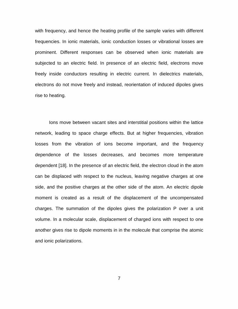
Ions move between vacant sites and interstitial positions within the lattice
network, leading to space charge effects. But at higher frequencies, vibration
losses from the vibration of ions become important, and the frequency
dependence of the losses decreases, and becomes more temperature
dependent [18]. In the presence of an electric field, the electron cloud in the atom
can be displaced with respect to the nucleus, leaving negative charges at one
side, and the positive charges at the other side of the atom. An electric dipole
moment is created as a result of the displacement of the uncompensated
charges. The summation of the dipoles gives the polarization P over a unit
volume. In a molecular scale, displacement of charged ions with respect to one
another gives rise to dipole moments in in the molecule that comprise the atomic
and ionic polarizations.
8
Fig. 1.1 Frequency dependence of different components of polarizability[18]
The ability of a material to absorb electrical potential energy or the
microwave field is determined by its complex permittivity. The real part of the
permittivity, '∈ , the depth of penetration of the microwaves into the material can
be given, and,the loss factor, "∈ [19], indicates the material's ability to store the
energy. tanδ is described as the loss tangent that suggests the capability of
material to convert the field or energy absorbed into heat.
9
1.1.e. High Z Materials
In the past, microwave anneal technology has been used to anneal boron
implanted Si with much success [20]. This study is unique compared to other
such work done due to the dopant activated is a higher Z material such as
arsenic implanted Si. Due to the higher Z nature of the dopant, greater activation
energy would be required to electrically activate the dopant. To provide energy
through heat to facilitate this action, the microwave field generated by a 1300 W,
2.45 GHz magnetron is insufficient. The Si sample by means of having a low
dielectric constant is heated by the microwave radiation by volumetric heating,
due to larger depth of penetration. With a high depth of penetration, DP, the
sample is incapable of being raised to high temperatures required for
recrystallization, 600 oC being the temperature for Si. The use of a high dielectric
assistor material called as a susceptor has been suggested. In this study, the
susceptor is a cylindrical structure made of Fe2O3 infused SiC surrounding
alumina. The composite structure has a high dielectric constant, and when tested
as stand-alone substance being subjected to the microwave radiation, it exhibits
rapid heating rate, indicating surface heating by means of low depth of
penetration, instead of volumetric heating that provides high depth of penetration.
The idea is to supply the heat to the Si sample in a conductive manner so that
the sample reaches the temperatures required for recrystallization, and
undergoes uniform damage repair due to the uniform absorption of microwaves.
10
1.2 METAL OXIDE BASED THIN FILM TRANSISTORS
In the past, amorphous or polycrystalline Si:H layer have been commonly
used as channel layers for most conventional TFTs in flat panel displays.
However, these TFTs have a lot of disadvantages such as low mobility (<1
cm2/V-s), and are sensitive to light [21]. As a result of which they have poor
efficiency of light transmittance and brightness. To obtain a TFT with high
mobility requires relatively high process temperature (> 300 °C), which makes it
difficult to fabricate them on flexible polymer substrates.
With this in mind most of the research is moving from silicon based TFTs
to amorphous metal-oxide semiconductors as channel layer and source/drain
electrodes [22]. These TFTs attract much attention due to their advantages such
as high mobility, and high transmittance [23-25]. A number of metal-oxide based
TFTs such as zinc oxide (ZnO), zinc tin oxide (ZIO), indium gallium oxide (IGO),
and indium gallium zinc tin oxide (IGZSO) have demonstrated high mobilities
even for room temperature fabrication [26,27]. Many TFTs were reported using
crystalline ZnO [28,29], or polycrystalline SnO2 [30], and In2O3 [31].
Recently the transparent electronics has emerged a new field of
technology. However to realize the transparent TFTs for flexible electronics,
amorphous films are more suitable than crystalline type, because amorphous
oxide films have added advantages such as low temperature deposition, good
film smoothness, low compressive stress, large area deposition by sputtering,
11
and uniformity of device 12 characteristics [32-34]. The fabrication of low-
temperature TFTs allows for flexible large area electronic devices such as
electronic paper and flexible display which are lightweight, flexible, and shock
resistant. However the fabrication of low temperature amorphous metal-oxide
TFTs results in a number of defects in the channel layer, insulator and interface.
The presence of these TFTs can be a latent problem (e.g., poor performance and
thermal instability). Hence, it becomes very important to improve the
performance/stability of these TFTs. In addition, it would be very useful to
understand the role of these defects on the performance and stability of these
metal-oxide TFTs. We have improved the performance of these TFTs by low
temperature long anneals. Low temperatures are preferred due to the
compatibility of the post fabrication process with flexible polymer substrates
targeted for flexible large area electronics.
1.3 SUMMARY
This comprehensive report presents the work done in achieving novel
processing techniques for thin films and thin film transistors. The characterization
techniques employed in understanding material and device properties before and
after various anneal techniques are discussed in chapter 2. Chapters 3 and 4
describe the low energy and shorter duration microwave processing of arsenic-
doped silicon compared to conventional anneal methods. An attempt is made to
understand the mechanism of microwave annealing of heavily ion implanted
12
silicon. Shorter processing times have been achieved with susceptor-assisted
hybrid microwave heating of the ion-implanted silicon. Ceramic composite
susceptors, made of alumina and silicon carbide (SiC), have been used to
achieve the required temperatures for repairing the lattice damage caused by As
doping and for the electrical activation of the dopants.
Chapter 5 presents a detail investigation of the performance of IZO TFTs
under thermal and bias stress tests. The effect of post process anneals and the
enhanced stability of the devices under thermal stresses as a result, is also
discussed in this chapter.
Chapter 6 discusses an in-depth study on the effect of illumination
stresses and degradation in performance of IGZO TFTs. Failure conditions have
been identified along with the corresponding nature of defects which assists in
suggesting suitable post fabrication processes.
Chapter 7 presents a comprehensive summary of the work done, and
suggests a future plan of work where detailed study of nature of defects in the
metal oxide based TFTs will be performed. Suitable post processing methods
including microwave anneal will be suggested based on the type of defects
encountered in this work.
13
Chapter 2
EXPERIMENTAL PROCEDURE
2.1. Sample Preparation
The base samples are p-type boron doped, 100 Ω-cm (100) orientated
silicon wafers cleaned using the Radio Corporation of America procedure. Eaton
Nova NV10-180 batch process ion implanter was used to implant the cleaned Si
wafers. Ion implantation was performed while orienting the wafers at 7o with
respect to the normal to the incident beam and with a 45o plane twist, so that ion
channeling can be minimized. One set of wafers was implanted at room
temperature (RT) using 30 keV As+ ions and a dose of 5×10¹⁴ As+ cm-2. Another
set of wafers was implanted using 30 keV As+ ions and a dose of 1×10¹⁵ As+ cm-2
dosage. The last set of samples was implanted with a dose of 180 keV 1×10¹⁵
As+ cm-2 ions.
Microwave annealing of different dosage arsenic implanted Si samples
was done in a single-frequency (2.45 GHz), 2.8×104 cm3 cavity applicator
microwave system equipped with a 1300 Watt magnetron source. The anneal
times ranged between 40-100 seconds for each sample type. A Raytek Compact
MID series pyrometer with a spectral response of 8–14 µm was used to monitor
the near surface temperature. The emissivity for the samples was adjusted by
careful calibration of the temperature read by the pyrometer against the
temperature monitored by a thermocouple.
14
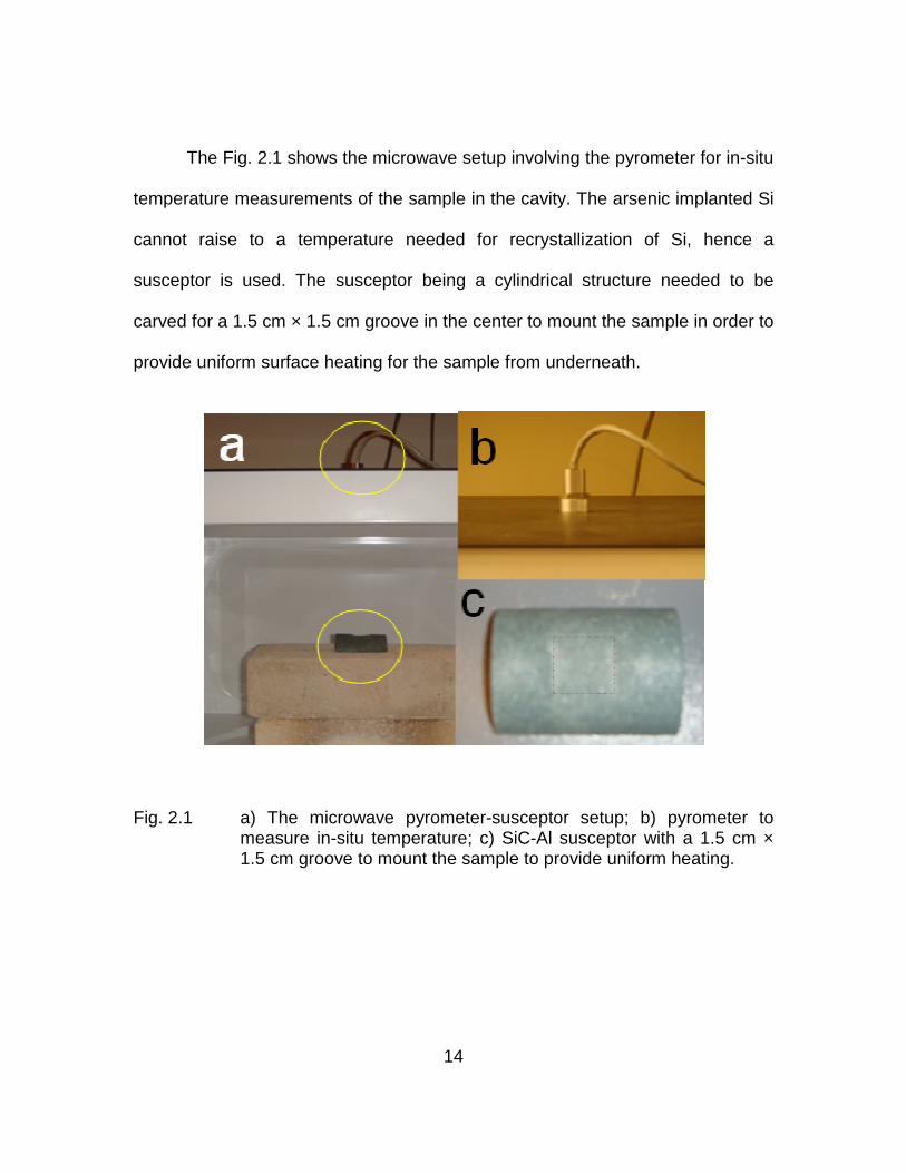
The Fig. 2.1 shows the microwave setup involving the pyrometer for in-situ
temperature measurements of the sample in the cavity. The arsenic implanted Si
cannot raise to a temperature needed for recrystallization of Si, hence a
susceptor is used. The susceptor being a cylindrical structure needed to be
carved for a 1.5 cm × 1.5 cm groove in the center to mount the sample in order to
provide uniform surface heating for the sample from underneath.
Fig. 2.1 a) The microwave pyrometer-susceptor setup; b) pyrometer to measure in-situ temperature; c) SiC-Al susceptor with a 1.5 cm × 1.5 cm groove to mount the sample to provide uniform heating.
15
2.2. Material Characterization
With the use of a susceptor to provide additional heating mechanism, the
surface temperatures of the arsenic implanted Si ranged between 620-680 oC.
The as-implanted As+ and the microwave annealed samples were characterized
using several methods to test for dopant activation and film recrystallization. In
addition to characterizing pre and post anneal samples for the aforementioned
criterion, the microwave annealed samples were compared against 30 second
rapid thermal annealed (RTA) samples, annealed at 900°C for the extent of
dopant diffusion. Microwave losses coupled with hybrid volumetric and surface
heating of the sample through microwave power absorption and susceptor
heating are the mechanisms behind recrystallization of the arsenic implanted Si.
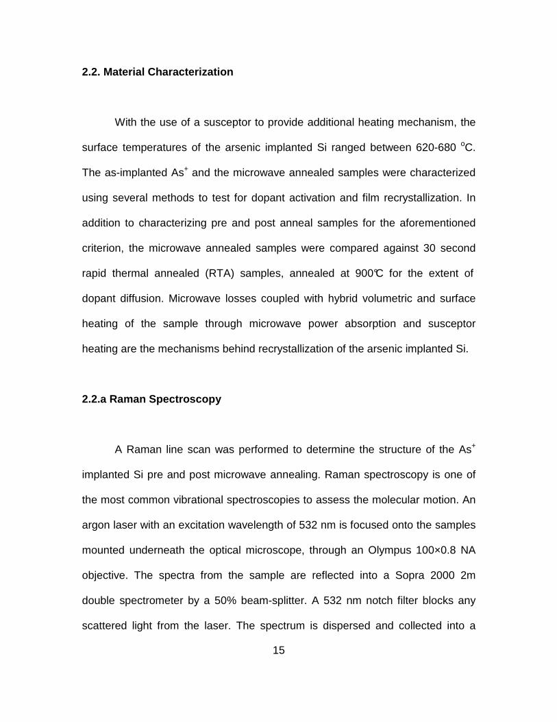
2.2.a Raman Spectroscopy
A Raman line scan was performed to determine the structure of the As+
implanted Si pre and post microwave annealing. Raman spectroscopy is one of
the most common vibrational spectroscopies to assess the molecular motion. An
argon laser with an excitation wavelength of 532 nm is focused onto the samples
mounted underneath the optical microscope, through an Olympus 100×0.8 NA
objective. The spectra from the sample are reflected into a Sopra 2000 2m
double spectrometer by a 50% beam-splitter. A 532 nm notch filter blocks any
scattered light from the laser. The spectrum is dispersed and collected into a
16
Princeton CCD Camera with an energy dispersion of 60pixels/cm. The Raman
spectra collected from the CCD is calibrated as a function of intensity that
depends on the time of exposure, against the relative wavenumber [35]. High
energy beam samples damage the sample surface, but in the Raman
spectroscopy, care is taken to avoid usage of high energy beams. The maximum
power of a beam used in Raman spectroscopy is 100 mW. In our setup, a 4 mW
power beam was used, which goes through a series of beam splitters, at the end
of which the beam power hitting the sample is as low as 1 mW which doesn’t
alter the characteristics of the sample. The setup of the Raman spectroscopy is
as seen in Fig. 2.2 below.
Fig. 2.2 Raman Spectrometer used for characterizing the samples to observe the crystalline structure (Courtesy: Center for Solid State Sciences, CSSS, ASU)
17
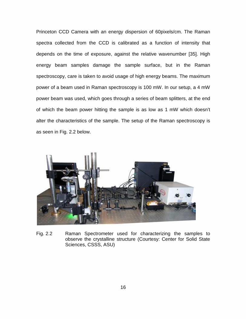
2.2.b Rutherford Backscattering Spectrometry
Rutherford backscattering spectrometry (RBS) is a non-destructive
characterization technique. It is used to analyze the atomic composition of the
sample like diffusion and interaction between the copper and ruthenium thin films
and to estimate the sample thickness using very high energy (MeV) beam of low
ion mass. It is also used for quantitative depth profiling, areal density
measurements, and determination of crystal lattice quality. RBS utilizes
Tandetron accelerator to generate a MeV ion beam. After entering the evacuated
beam line, the ions are then collimated and focused. There are bending magnets
which after mass selection geometrically disperse ions according to their mass.
Finally the beam raster-scans over the specimen and back scattered ions are
analyzed by a Si barrier detector. The electronic pulses are then amplified and
sorted according to the voltage amplitude by a multichannel analyzer to yield the
resulting RBS spectrum [36]. RBS was performed using a General Ionex 1.7 MV
tandem accelerator with He2+ ions at energy of 2.8 or 3.5 MeV as shown in Fig.
2.3.
Ion implantation with concentrations and energies such as of the samples
in our study causes implant damage. Ion channeling experiments were
conducted to compare the damage in unannealed samples as opposed to
processed samples, and to ascertain if the microwave annealing could repair
damage of this extent. Rutherford backscattering spectrometry (RBS) was used
18
to quantify the implant damage, and a 2.0 MeV He+ analyzing beam for ion
channeling. Samples were analyzed in random and [001] channeled orientations.
He+ ions were collected using a solid state detector, positioned 13o from the
incident beam. The software program RUMP was used to simulate layer
thicknesses from RBS data.
Fig. 2.3 Schematic of a typical Rutherford backscattering Spectrometry instrumentation system.
RBS spectrum
Energy
Cou
nts
Multichannel analyzer
Amplifier
Preamplifier
Target
Beam
RBS ChamberCollimators
MagnetAccelerator
Detector
Vacuum beam line
19
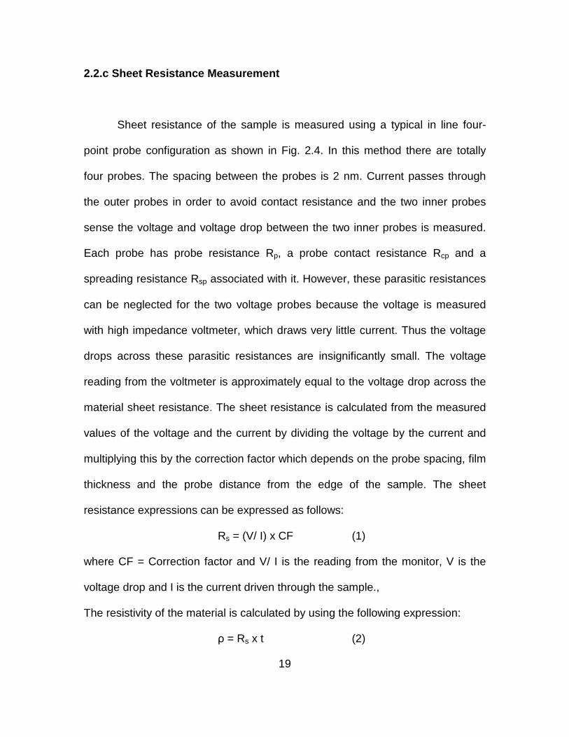
2.2.c Sheet Resistance Measurement
Sheet resistance of the sample is measured using a typical in line four-
point probe configuration as shown in Fig. 2.4. In this method there are totally
four probes. The spacing between the probes is 2 nm. Current passes through
the outer probes in order to avoid contact resistance and the two inner probes
sense the voltage and voltage drop between the two inner probes is measured.
Each probe has probe resistance Rp, a probe contact resistance Rcp and a
spreading resistance Rsp associated with it. However, these parasitic resistances
can be neglected for the two voltage probes because the voltage is measured
with high impedance voltmeter, which draws very little current. Thus the voltage
drops across these parasitic resistances are insignificantly small. The voltage
reading from the voltmeter is approximately equal to the voltage drop across the
material sheet resistance. The sheet resistance is calculated from the measured
values of the voltage and the current by dividing the voltage by the current and
multiplying this by the correction factor which depends on the probe spacing, film
thickness and the probe distance from the edge of the sample. The sheet
resistance expressions can be expressed as follows:
Rs = (V/ I) x CF (1)
where CF = Correction factor and V/ I is the reading from the monitor, V is the
voltage drop and I is the current driven through the sample.,
The resistivity of the material is calculated by using the following expression:
ρ = Rs x t (2)
20
where t = thickness of the material. This measurement was of particular interest
to verify that the resistance of the alloy films after annealing was comparable to
that of the as-deposited sample.
Fig. 2.4 Layout of atypical four-point probe setup. Measurements taken at ASU had a probe spacing of 2 mm. Where S = spacing between the probes, and t = thickness of the sample.
V
s

21
2.2.d Hall Measurements
In order to determine if there was any carrier inversion that occurred after
microwave annealing, Hall measurement testing was performed over the
samples before and after annealing.using Van der Pauw method. To do so, the
samples were mounted onto a printed circuit board by making aluminum deposits
for contacts, and using copper wires and silver paste to establish contacts.
The Van der Pauw method is the most common technique used to
accurately measure electrical properties of a sample such as the resistivity,
doping of the material whether it is p-type or n-type doped, the mobility of the
majority carriers, and the sheet carrier densities. To be able to use the Van der
Pauw method, the sample thickness needs to be much less than the length and
width of the sample, which means, the sample needs to be 2 dimensional. To
reduce errors in the measurement, the sample should be made symmetrical,
most often a square shaped one. The contacts for the measurement need to be
made appropriately too, and the material for contact should be chosen in such a
way that an ohmic contact can be made. Silver is used to make contact with
between the copper wires and the sample material. But for silicon substrates,
silver cannot make an ohmic contact directly, hence aluminum was deposited
using an evaporator system and masks, just at the corners of the sample, and
silver can then be used to make the contact with copper wires.
22
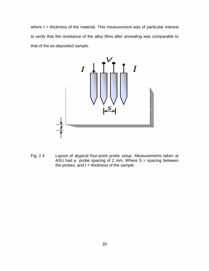
In order to use the Van der Pauw method, the sample thickness must be
much less than the width and length of the sample. In order to reduce errors in
the calculations, it is preferable that the sample is symmetrical. There must also
be no isolated holes within the sample. From the top left corner of the sample, if
the contacts are numbered 1 to 4 in a counter-clockwise direction as seen in Fig.
2.5, current is made to flow along one edge of the sample (along the 1-2 side),
and voltage is noted on the other edge (along the 3-4 side).
Fig. 2.5 Sample labeling for the contacts made to perform van der Pauw Hall measurements.
1
2 3
4

23
The ratio of the voltage V34 and I12.gives the resistance in the material
R =
34
12
VI (3)
Hall measurements, as the name suggests, make use of the Hall effect in
electrical characterization of the material. When electrons flow through a
magnetic field, a force called Lorentz force is exerted on them which depends on
the velocity of their motion in the field. The force is maximum when the field is
perpendicular to the motion of the electrons, and is given by
FL = q.υ.B (4)
where q = the charge on the particle in coulombs
υ = velocity
B = the strength of the magnetic field (Wb/cm2)
Applying current on a semiconductor material results in a steady state flow of
electrons within the material, with a velocity given by
υ = 1
m m n µ q (5)
where n = electron density
A = cross-sectional area of the material
q = 1.6 × 10⁻¹⁹ coulombs
The force leads to accumulation of charges along an edge and creates an
electric field induced produce accumulation of electrons along an edge, and the
hall voltage can be directly extracted from this field, given by
24
VH = ω Є (6)
= nqdIB
d=depth of the material
= s n q
IB
Hence, we can obtain the sheet density ns from the hall voltage. From previously
obtained resistivity measurements, sheet resistance of the material is known
from which the mobility of the material is given by
µ = 1
s sn q R (7)
Finally the resistivity of the material is given by
ρ = 1
m m n µ q (8)
where nm = doping level of majority carrier
µm = mobility of the majority carrier
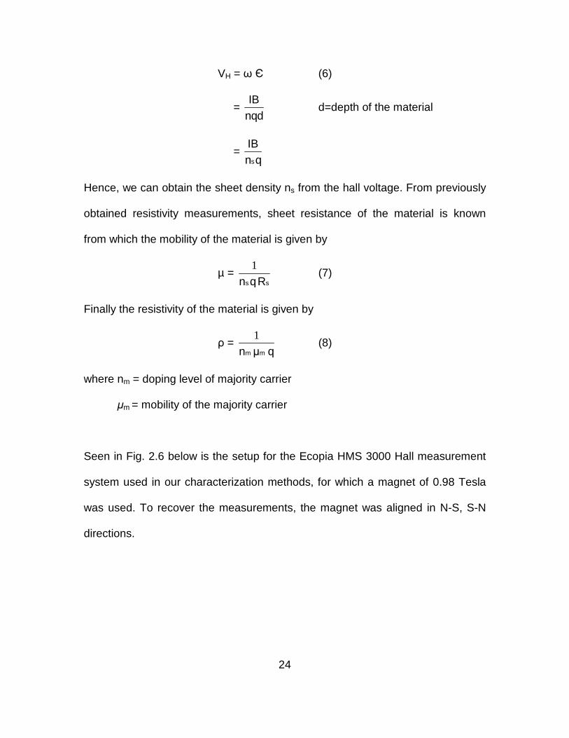
Seen in Fig. 2.6 below is the setup for the Ecopia HMS 3000 Hall measurement
system used in our characterization methods, for which a magnet of 0.98 Tesla
was used. To recover the measurements, the magnet was aligned in N-S, S-N
directions.
25
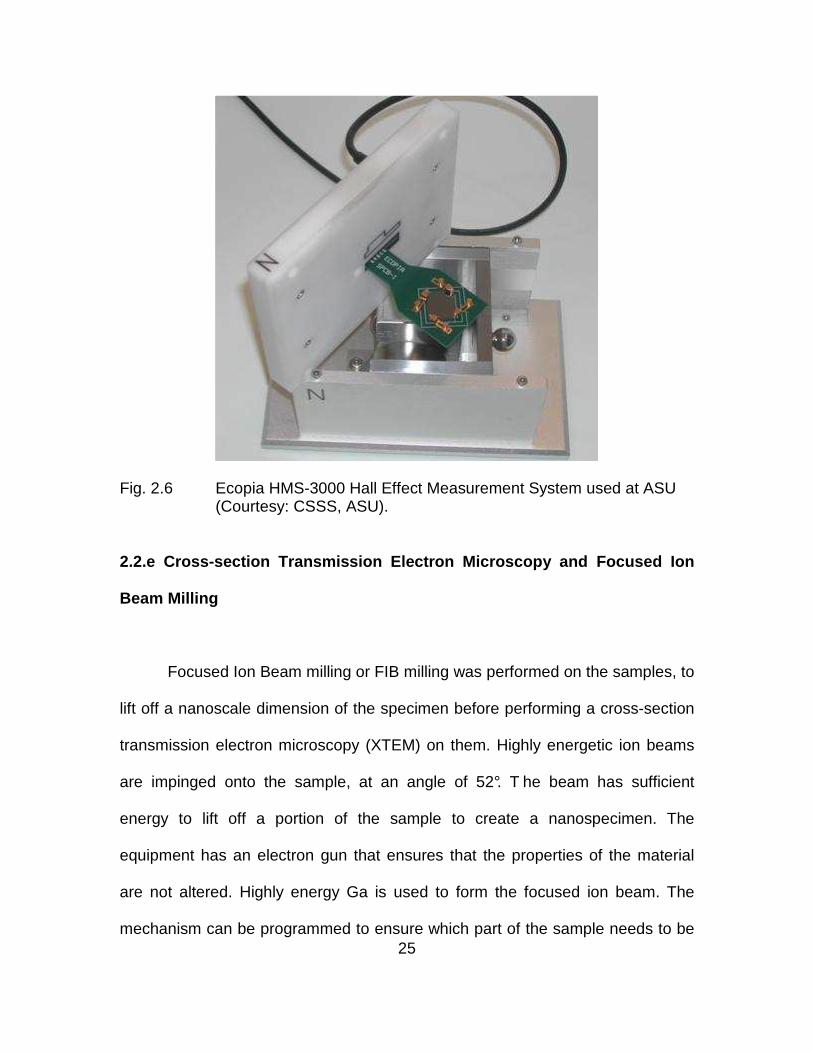
Fig. 2.6 Ecopia HMS-3000 Hall Effect Measurement System used at ASU (Courtesy: CSSS, ASU).
2.2.e Cross-section Transmission Electron Microscopy and Focused Ion
Beam Milling
Focused Ion Beam milling or FIB milling was performed on the samples, to
lift off a nanoscale dimension of the specimen before performing a cross-section
transmission electron microscopy (XTEM) on them. Highly energetic ion beams
are impinged onto the sample, at an angle of 52°. T he beam has sufficient
energy to lift off a portion of the sample to create a nanospecimen. The
equipment has an electron gun that ensures that the properties of the material
are not altered. Highly energy Ga is used to form the focused ion beam. The
mechanism can be programmed to ensure which part of the sample needs to be
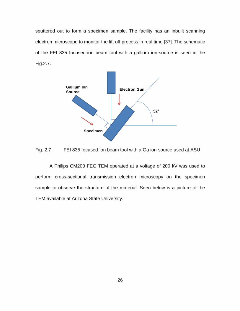
26
sputtered out to form a specimen sample. The facility has an inbuilt scanning
electron microscope to monitor the lift off process in real time [37]. The schematic
of the FEI 835 focused-ion beam tool with a gallium ion-source is seen in the
Fig.2.7.
Fig. 2.7 FEI 835 focused-ion beam tool with a Ga ion-source used at ASU
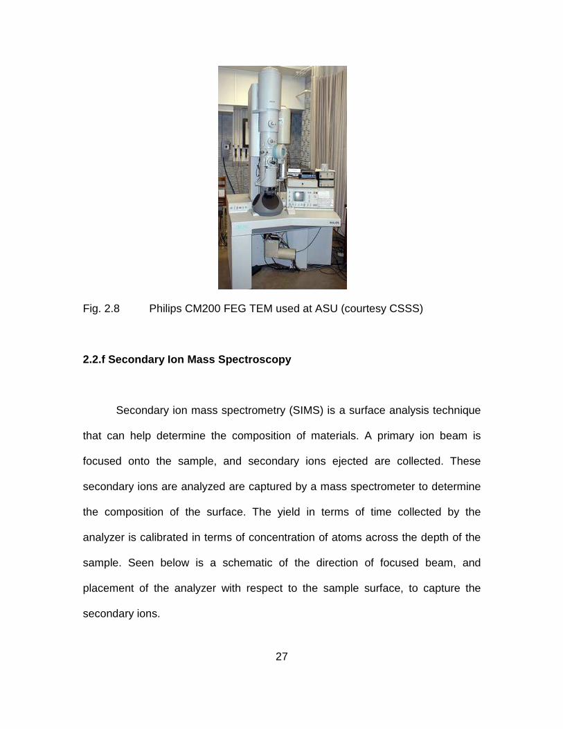
A Philips CM200 FEG TEM operated at a voltage of 200 kV was used to
perform cross-sectional transmission electron microscopy on the specimen
sample to observe the structure of the material. Seen below is a picture of the
TEM available at Arizona State University..
Electron Gun
Specimen
Gallium Ion Source
52°
27
Fig. 2.8 Philips CM200 FEG TEM used at ASU (courtesy CSSS)
2.2.f Secondary Ion Mass Spectroscopy
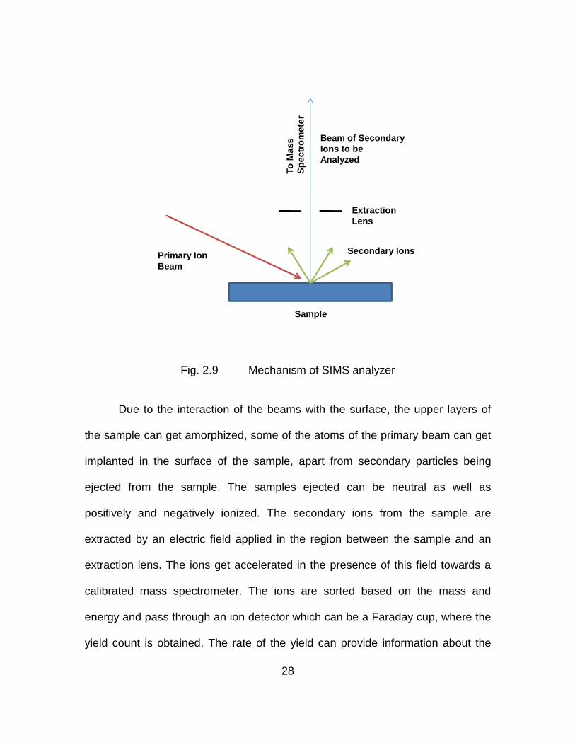
Secondary ion mass spectrometry (SIMS) is a surface analysis technique
that can help determine the composition of materials. A primary ion beam is
focused onto the sample, and secondary ions ejected are collected. These
secondary ions are analyzed are captured by a mass spectrometer to determine
the composition of the surface. The yield in terms of time collected by the
analyzer is calibrated in terms of concentration of atoms across the depth of the
sample. Seen below is a schematic of the direction of focused beam, and
placement of the analyzer with respect to the sample surface, to capture the
secondary ions.
28
Fig. 2.9 Mechanism of SIMS analyzer
Due to the interaction of the beams with the surface, the upper layers of
the sample can get amorphized, some of the atoms of the primary beam can get
implanted in the surface of the sample, apart from secondary particles being
ejected from the sample. The samples ejected can be neutral as well as
positively and negatively ionized. The secondary ions from the sample are
extracted by an electric field applied in the region between the sample and an
extraction lens. The ions get accelerated in the presence of this field towards a
calibrated mass spectrometer. The ions are sorted based on the mass and
energy and pass through an ion detector which can be a Faraday cup, where the
yield count is obtained. The rate of the yield can provide information about the
Extraction Lens
Beam of Secondary Ions to beAnalyzed
Secondary IonsPrimary Ion Beam
Sample
To M
ass
Sp
ectr
om
eter
29
composition of the material. The SIMS technique is useful for all elements except
noble gases since they don’t ionize easily.
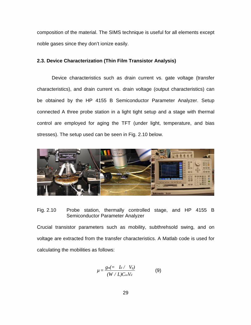
2.3. Device Characterization (Thin Film Transistor Analysis)
Device characteristics such as drain current vs. gate voltage (transfer
characteristics), and drain current vs. drain voltage (output characteristics) can
be obtained by the HP 4155 B Semiconductor Parameter Analyzer. Setup
connected A three probe station in a light tight setup and a stage with thermal
control are employed for aging the TFT (under light, temperature, and bias
stresses). The setup used can be seen in Fig. 2.10 below.
Fig. 2.10 Probe station, thermally controlled stage, and HP 4155 B Semiconductor Parameter Analyzer
Crucial transistor parameters such as mobility, subthrehsold swing, and on
voltage are extracted from the transfer characteristics. A Matlab code is used for
calculating the mobilities as follows:
m d g
ox d
g (= I / V )µ =
(W / L)C V
∂ ∂ (9)
30
Aging conditions used in this research are a) illumination stress testing under
wavelengths within the visible range of the spectrum, b) thermal stressing at 20
°C, 50 °C, and 80 °C, and c) bias stress testing un der gate voltages of ± 20 V,
and drain voltages of 0, 20 V. A combination of conditions a and c, and b and c
are used to understand the effect of extreme stresses towards driving the
transistors into extreme degradation or even failure.
31
Chapter 3
DOPANT ACTIVATION AND DIFFUSION PROFILE OF ARSENIC IMPLANTED
SILICON
3.1. Introduction
To perform quick regrowth or dopant activation by post implantation
processing , the semiconductor is intentionally adulterated with additional dopant
or metal atoms [38] which act as localized heating spots when annealed, raising
to higher temperatures quicker than the semiconductor atoms due to their
specific heat properties and Fermi level effects. Regrowth rate becomes greater
with temperature, and hence shorter times suffice for recrystallization. Over the
years there has been success in the development of processes which achieve
this high temperature in shorter hours, and some even in seconds (e.g., RTA),
but without adulterating the sample in order to do so. In this study we have used
microwave annealing (by using a SiC susceptor/assistor) to achieve a high
quality crystalline Si layer in much shorter times, and have compared it against
the samples treated using RTA, to verify the reduced extent of end-of-range
diffusion. This shallower dopant profile over RTA confirms the potential use of
susceptor assisted microwave annealing for dopant activation and solid phase
regrowth. The assistor, as the name suggests, is used to supply additional heat
to the sample for it to reach the desired temperature range in a shorter time. This
study discusses the mechanism of this heat supply, and the quality of the results
32
produced, if they are better than the results obtained from methods mentioned
before.
3.2. Experimental procedure
The base samples are p-type boron doped, 100 Ω-cm (100) orientated
silicon wafers cleaned using the Radio Corporation of America procedure. Eaton
Nova NV10-180 batch process ion implanter was used to implant the cleaned Si
wafers. Ion implantation was performed while orienting the wafers at 7o with
respect to the normal to the incident beam and with a 45o plane twist, so that ion
channeling can be minimized. One set of wafers was implanted at room
temperature (RT) using 30 keV As+ ions and a dose of 5×10¹⁴ As+ cm-2. Another
set of wafers was implanted using 30 keV As+ ions and a dose of 1×10¹⁵ As+ cm-2
dosage. The last set of samples was implanted with a dose of 180 keV 1×10¹⁵
As+ cm-2 ions. Microwave annealing of different dosage arsenic implanted Si
samples was done in a single-frequency (2.45 GHz), 2.8×104 cm3 cavity
applicator microwave system equipped with a 1300 Watt magnetron source. The
anneal times ranged between 40-100 seconds for each sample type. A Raytek
Compact MID series pyrometer with a spectral response of 8–14 µm was used to
monitor the near surface temperature. The emissivity for the samples was
adjusted by careful calibration of the temperature read by the pyrometer against
the temperature monitored by a thermocouple. For the arsenic implanted
samples, the surface temperatures ranged 620-680 oC
33
Ion implantation with concentrations and energies such as of the samples
in our study causes implant damage. Ion channeling experiments were
conducted to compare the damage in unannealed samples as opposed to
processed samples, and to ascertain if the microwave annealing could repair
damage of this extent. Rutherford backscattering spectrometry (RBS) was used
to quantify the implant damage, and a 2.0 MeV He+ analyzing beam for ion
channeling. Samples were analyzed in random and [001] channeled orientations.
He+ ions were collected using a solid state detector, positioned 13o from the
incident beam. The software program RUMP was used to simulate layer
thicknesses from RBS data.
To test for any electrical dopant activation, the samples were placed face
up under an in-line 4 point probe reading out to a 100 mA Keithley 2700 digital
multimeter. The sheet resistances (Rsh) of the samples were carefully tabulated
for every process time. In order to determine if there was any carrier inversion
that occurred after microwave annealing, Hall measurement testing was
performed over the samples before and after annealing using Van der Pauw
method. To do so, the samples were mounted onto a printed circuit board by
making aluminum deposits for contacts, and using copper wires and silver paste
to establish contacts.
34
Secondary ion mass spectroscopy (SIMS) was performed to capture the
secondary As+ ions from the sample across its depth. The results observed as a
function of the yield with time were calibrated to give a measure of the density of
As+ across the depth of the sample. The plot of As+ density as a function of Si
depth gives a measure of the extent of diffusion of the dopant for the microwave
annealed samples and for RTA annealed samples.
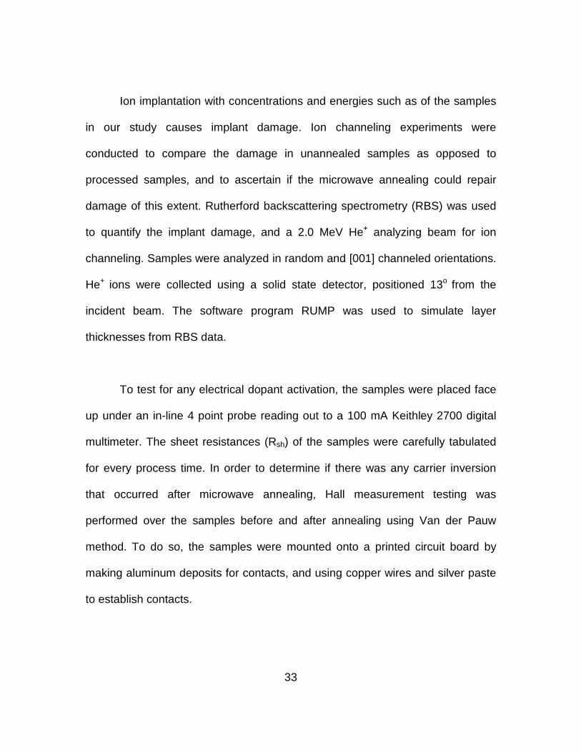
3.3. Results
The anneal time in the study is defined as the duration between when the
microwave is switched on and when the microwave is turned off. The
temperature profile of the samples suggests that stand alone microwave heating
is not sufficient for the samples to reach the required temperatures of around 600
oC as mentioned earlier, since a-Si cannot absorb microwave energy at low
temperatures [16], and supports our incentive of using an additional heating
material in the setup to enable the samples to absorb the microwave radiation.
Inspection of Fig. 3.1 reveals how microwave radiation assisted by the alumina
coated silicon carbide (SiC-alumina) susceptor [16,39], allows for rapid heating
and confirms that microwave annealing without a susceptor does not help the
sample obtain a high temperature.
35
Fig. 3.1 Temperature vs Time profile of As implanted Si with and without susceptor
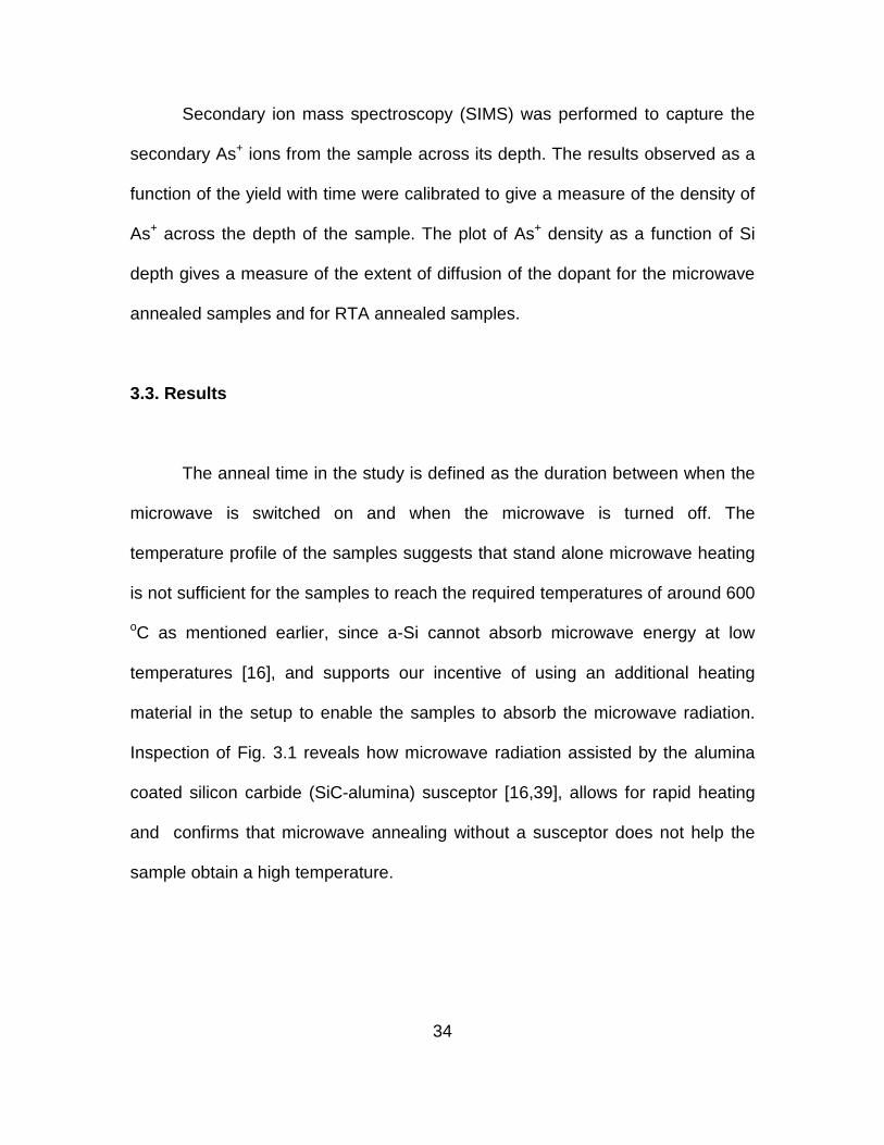
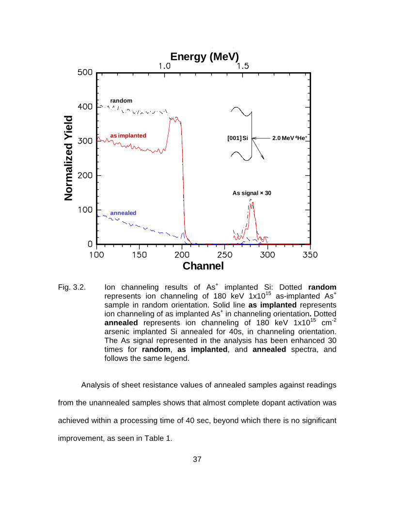
The spectra random and as-implanted in Fig. 3.2 present RBS results
obtained from the as-implanted samples in a random orientation and a [001]
channeling orientation, respectively. The energetic arsenic ions create a thin
damaged Si layer and amorphize the crystalline Si. Both the plots show the
lattice damage due to ion implantation, and also a magnified (× 30) As peak
around channel number 280 [39], that confirms arsenic is located off the lattice
sites instead of at the substitutional sites [20]. A comparison of the normalized
yield of aligned channeling spectrum against the normalized yield of random
36
spectra gives the order of lattice damage. The factor is denoted by χmin [40].
Channeling spectrum annealed presents ion channeling results of the samples in
a [001] channeling orientation after 40 sec microwave annealing. The χmin for
annealed is 0.11 implying that the lattice damage was repaired to a great extent.
The ion channeling yield of a 70 sec annealed sample (not shown), also has a
χmin of around 0.11 confirming that the improvement in lattice damage repair is
insignificant over a 40 sec microwave anneal. The results signify that the dopant
atoms are now essentially located in substitutional sites instead of off-lattice
sites, as in the as-implanted channeled spectrum in Fig. 3.2. This repair of lattice
damage, and dopant relocation, are key factors that lead to dopant activation and
reduced sheet resistance of the arsenic implanted Silicon samples. The spectra
of 180 keV arsenic implanted samples, confirms deeper lattice damage, and
thicker damaged surface layer. However great the damage, a 40 second anneal
would still suffice to repair the lattice implant damage, and distribute the dopant
atoms to substitutional sites in the lattice.
37
Fig. 3.2. Ion channeling results of As+ implanted Si: Dotted random represents ion channeling of 180 keV 1x10¹⁵ as-implanted As+ sample in random orientation. Solid line as implanted represents ion channeling of as implanted As+ in channeling orientation. Dotted annealed represents ion channeling of 180 keV 1x1015 cm-2 arsenic implanted Si annealed for 40s, in channeling orientation. The As signal represented in the analysis has been enhanced 30 times for random, as implanted, and annealed spectra, and follows the same legend.
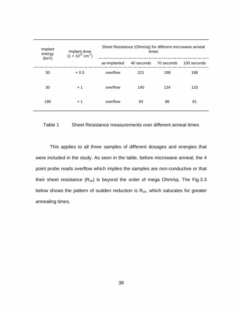
Analysis of sheet resistance values of annealed samples against readings
from the unannealed samples shows that almost complete dopant activation was
achieved within a processing time of 40 sec, beyond which there is no significant
improvement, as seen in Table 1.
random
as implanted
annealed
As signal × 30
2.0 MeV 4He+[001] Si
Channel
Energy (MeV)N
orm
aliz
ed Y
ield
38
Implant energy (keV)
Implant dose (1 × 1015 cm-2)
Sheet Resistance (Ohm/sq) for different microwave anneal
times
as-implanted 40 seconds 70 seconds 100 seconds
30 × 0.5 overflow 221 198 188
30 × 1 overflow 140 134 133
180 × 1 overflow 93 86 81
Table 1 Sheet Resistance measurements over different anneal times
This applies to all three samples of different dosages and energies that
were included in the study. As seen in the table, before microwave anneal, the 4
point probe reads overflow which implies the samples are non-conductive or that
their sheet resistance (Rsh) is beyond the order of mega Ohm/sq. The Fig.3.3
below shows the pattern of sudden reduction is Rsh, which saturates for greater
annealing times.
39
Fig. 3.3 Sheet Resistance measurements of the different dosage and implantation energy As implanted Si at different anneal times.
The Hall measurements show the inversion of carriers from p-type before
annealing, which is from the heavily boron doped substrate, to being n-type from
the arsenic that was implanted onto Si samples. Due to the heavy doping that
causes degenerate sheet concentration values, ion scattering becomes dominant
in the surface, reducing the mobilities after annealing, which were otherwise
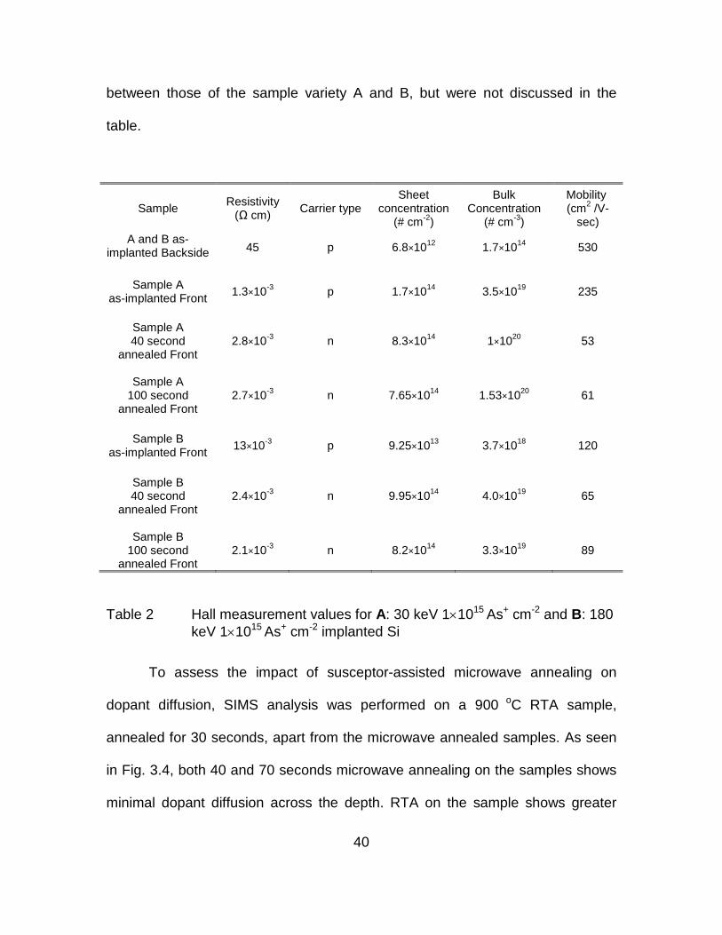
expected to be high. Table 2 summarizes the resistivities, sheet and bulk
concentrations, and mobilities of 30 keV 1×10¹⁵ As+ cm-2 and 180 keV 1×10¹⁵ As+
cm-2 implanted Si samples. The values of the 30 keV 1×10¹⁴ As+ cm-2 fell
40
between those of the sample variety A and B, but were not discussed in the
table.
Sample Resistivity
(Ω cm) Carrier type
Sheet concentration
(# cm-2)
Bulk Concentration
(# cm-3)
Mobility (cm2 /V-
sec)
A and B as-implanted Backside 45 p 6.8×10¹² 1.7×10¹⁴ 530
Sample A
as-implanted Front 1.3×10⁻³ p 1.7×10¹⁴ 3.5×10¹⁹ 235
Sample A 40 second
annealed Front 2.8×10⁻³ n 8.3×10¹⁴ 1×10²⁰ 53
Sample A
100 second annealed Front
2.7×10⁻³ n 7.65×10¹⁴ 1.53×10²⁰ 61
Sample B
as-implanted Front 13×10-3 p 9.25×10¹³ 3.7×10¹⁸ 120
Sample B 40 second
annealed Front 2.4×10⁻³ n 9.95×10¹⁴ 4.0×10¹⁹ 65
Sample B
100 second annealed Front
2.1×10⁻³ n 8.2×10¹⁴ 3.3×10¹⁹ 89
Table 2 Hall measurement values for A: 30 keV 1×10¹⁵ As+ cm-2 and B: 180 keV 1×10¹⁵ As+ cm-2 implanted Si
To assess the impact of susceptor-assisted microwave annealing on
dopant diffusion, SIMS analysis was performed on a 900 oC RTA sample,
annealed for 30 seconds, apart from the microwave annealed samples. As seen
in Fig. 3.4, both 40 and 70 seconds microwave annealing on the samples shows
minimal dopant diffusion across the depth. RTA on the sample shows greater
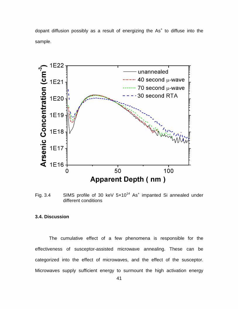
41
dopant diffusion possibly as a result of energizing the As+ to diffuse into the
sample.
Fig. 3.4 SIMS profile of 30 keV 5×10¹⁴ As+ impanted Si annealed under different conditions
3.4. Discussion
The cumulative effect of a few phenomena is responsible for the
effectiveness of susceptor-assisted microwave annealing. These can be
categorized into the effect of microwaves, and the effect of the susceptor.
Microwaves supply sufficient energy to surmount the high activation energy
42
needed for lattice damage repair and bring about dopant activation, without
causing dopant diffusion, all in a short duration. For dopant activation of arsenic
to be achieved, the As need to replace Si in the substitutional sites. Our ion
channeling results also show that the dopant atoms now occupy substitutional
lattice sites suggesting successful dopant activation.
The mechanism underlying the heating of the sample is microwave power
loss. Microwave power converts into heat based on the property of the material
defined as effective loss factor, which comprises conduction and polarization
losses [41]. Depending on the dielectric constant of the sample, the power
absorbed and the depth of absorption of the microwave radiation vary [42]. The
power thus absorbed is converted into heat based on the specific heat capacity
value of the sample. The sample in discussion is arsenic doped Si, As having a
CP of 326 J/Kg-K, and Si having a CP of 710 J/Kg-K.
Apart from the dielectric constant, the dielectric loss factor of a material is
another property that decides its absorption capability. Materials with high
dielectric loss factor can absorb microwave radiation better. Thus, considering
only the effect of microwave radiation, which provides volumetric heating, the
power absorbed per unit volume is given by equation 1 as
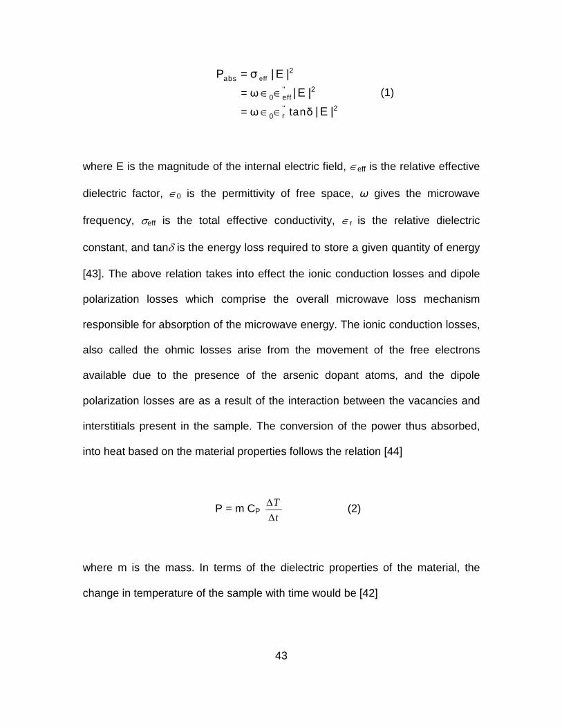
43
∈ ∈
∈ ∈
eff2
abs
'' 20 eff
'' 2r0
= ω
= ω tanδ
P = σ | E |
| E |
|E |
(1)
where E is the magnitude of the internal electric field, ∈eff is the relative effective
dielectric factor, ∈0 is the permittivity of free space, ω gives the microwave
frequency, σeff is the total effective conductivity, ∈r is the relative dielectric
constant, and tanδ is the energy loss required to store a given quantity of energy
[43]. The above relation takes into effect the ionic conduction losses and dipole
polarization losses which comprise the overall microwave loss mechanism
responsible for absorption of the microwave energy. The ionic conduction losses,
also called the ohmic losses arise from the movement of the free electrons
available due to the presence of the arsenic dopant atoms, and the dipole
polarization losses are as a result of the interaction between the vacancies and
interstitials present in the sample. The conversion of the power thus absorbed,
into heat based on the material properties follows the relation [44]
P = m CP T
t
∆∆
(2)
where m is the mass. In terms of the dielectric properties of the material, the
change in temperature of the sample with time would be [42]
44
'' 20 tan | |
mass P
rT
t C
Eω δρ
∆∆
∈∈= (3)
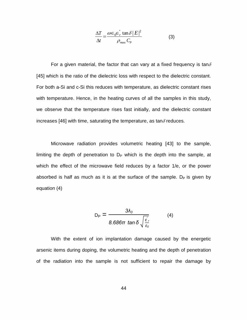
For a given material, the factor that can vary at a fixed frequency is tanδ
[45] which is the ratio of the dielectric loss with respect to the dielectric constant.
For both a-Si and c-Si this reduces with temperature, as dielectric constant rises
with temperature. Hence, in the heating curves of all the samples in this study,
we observe that the temperature rises fast initially, and the dielectric constant
increases [46] with time, saturating the temperature, as tanδ reduces.
Microwave radiation provides volumetric heating [43] to the sample,
limiting the depth of penetration to DP which is the depth into the sample, at
which the effect of the microwave field reduces by a factor 1/e, or the power
absorbed is half as much as it is at the surface of the sample. DP is given by
equation (4)
DP = 3λ0
8.686π tan δ ε
r
ε0
(4)
With the extent of ion implantation damage caused by the energetic
arsenic items during doping, the volumetric heating and the depth of penetration
of the radiation into the sample is not sufficient to repair the damage by
45
nucleation followed by growth. Furthermore, arsenic being a high Z material
requires a higher temperature to absorb the microwaves.
The advantages of microwave radiation can be applied to our As
implanted Si samples and other high Z implanted samples, by including an
additional assisting system, that can help the sample obtain a temperature where
it can absorb the microwave radiation and further convert the power to heat. The
susceptor surely pronounces its effect in the arsenic implanted Si samples, by
acting as a source of additional heat, but does not negate the underlying impact
of microwave radiation, hence making it an assisted annealing method.
3.5. Conclusion
Through this study, we were able to elucidate in detail how microwave
loss mechanisms, high activation energies, and the susceptor, all combine to
achieve an electrically active arsenic doped Si thin film layer. Susceptor assisted
microwave annealing also proved better than the widely used RTA method, since
it led to very low dopant diffusion across the film. With some more improvements,
this technique would be a promising replacement in the semiconductor industry.
46
Chapter 4
RECRYSTALLIZATION OF ARSENIC AND as-IMPLANTED SILICON
4.1. Introduction
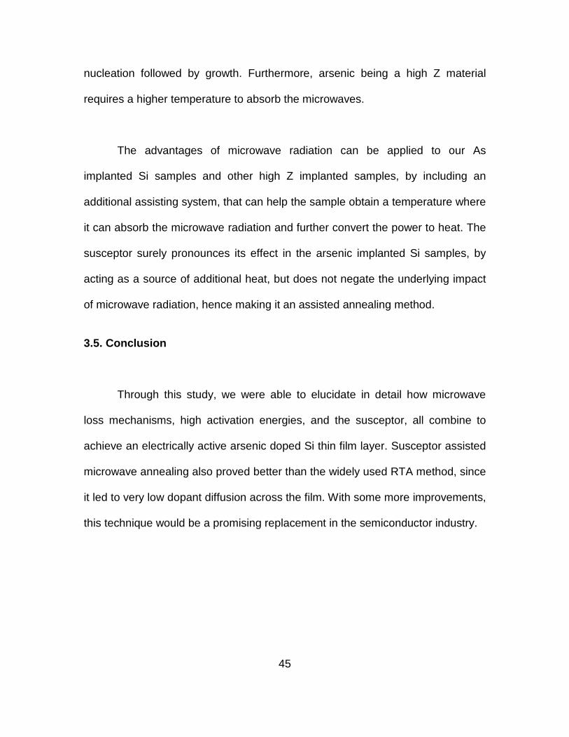
Inorder to compare the temperature profiles of a doped sample versus self
implanted Si sample without the influence of a susceptor, an as-implanted Si with
75 keV implantation energy, and 2×1015 cm- 2 Si+ dosage was also chosen.
Figure 4.1 shows a typical plot of temperature as a function of anneal time for a)
180 keV, 1×10¹⁵ As+ cm- 2 implanted Si sample and b) 75 keV, 2×1015 cm- 2 as
implanted Si+, both samples annealed for 2 minutes without a susceptor. The
anneal time in the study is defined as the duration between when the microwave
is switched on and when the microwave is turned off. The temperature profile of
these samples suggests that stand alone microwave heating is not sufficient for
them to reach the required temperatures of around 600 oC as mentioned earlier
since a-Si cannot absorb microwave energy at low temperatures [16], and
necessitates the use of an additional heating material in the setup to enable the
samples to absorb the microwave radiation.
47
Fig. 4.1 Temperature vs time profile of As implanted Si and as-implanted Si without a susceptor.
48
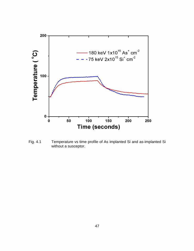
Fig. 4.2 Temperature vs time profile of As implanted Si and as-implanted Si witht a susceptor.
The samples in discussion are arsenic doped Si and as-implanted Si, As
having a CP of 326 J/Kg-K, and Si having a CP of 710 J/Kg-K. But an atom of Si
heats to a higher temperature than an atom of arsenic for the same power
absorbed, since Si weighs lesser than arsenic, and the mCP (Si) < mCP (As). The
effect of CP on heating rate without the assistance of a susceptor can be noticed
in Fig.4.1. In order to create the same extent of damage as 180 keV 1×1015 cm-2
arsenic implanted Si, the as-implanted Si was formed by implanting with 75 keV
2×1015 cm-2 Si+. The dosage [47] of Si+ chosen produced the same depth of the
49
damage layer as did the As+ implantation, and the energy required was in
correspondence with the TRIM [48] simulated implant projection range (RP) to
provide a similar depth of damage within the sample. Figure 4.1 compares the
heating rate of both these samples without a susceptor, and confirms our theory
that with the same damage and negating the impact of the susceptor, the as-
implanted Si+ heats faster than as-implanted As+. The results presented in the
figure also support our argument that materials with higher Z require assisted
heating. For the same samples, when a susceptor was included in the anneal
setup , the heating rates overlapped, suggesting that the effect of higher Z and
differences in the factor mCP have been overridden by the heat provided by the
susceptor, as seen in Fig.4.2. The dielectric properties of the susceptor are
responsible for this enhanced supply of heat to the mounted samples.
4.2. Structural Characterization
The as-implanted As+ and the microwave annealed samples were
characterized using several methods to test for dopant activation and film
recrystallization. A Raman line scan was performed to determine the structure of
the As+ implanted Si pre and post microwave annealing. An argon laser with an
excitation wavelength of 532 nm is focused onto the samples mounted
underneath the optical microscope, through an Olympus 100×0.8 NA objective.
The spectra from the sample are reflected into a Sopra 2000 2m double
spectrometer by a 50% beam-splitter. A 532 nm notch filter blocks any scattered
50
light from the laser. The spectrum is dispersed and collected into a Princeton
CCD Camera with an energy dispersion of 60pixels/cm. The Raman spectra
collected from the CCD is calibrated as a function of intensity that depends on
the time of exposure, against the relative wavenumber [35].
Ion channeling experiments were carried on for as-implanted Si samples
with and without susceptor annealed for different times to verify once again if
anneal without susceptor is capable of damage repair, and to compare the lattice
damage repair by anneal with susceptor.
To observe the microstructure of the sample before and after annealing,
cross-section transmission electron microscopy (XTEM) was performed using a
Philips CM200 FEG TEM operated at a voltage of 200 kV. Enhancement of
defect contrast was provided by 220 bright-field and dark-field imaging. TEM
samples were prepared using a FEI835 focused-ion beam tool with a gallium ion-
source.
51
4.3. Results
Raman spectra were obtained from as-implanted and annealed samples
of 1×1015cm-2 dose As+ implanted with energy of 30 keV. In Fig.4.3 the 480 cm-1
broad peak is attributed to an amorphous Si layer in the unannealed samples.
The Raman spectra of the annealed samples however, do not possess this
peak, but instead possess a 520 cm-1 single crystal Si peak [16], indicating that
crystallization of the as-implanted layer is not only initiated, but has been
completed within 40 sec of the anneal. The smaller full width half maximum
(FWHM) value implies well recrystallized Si which is the preferable outcome.
Fig. 4.3 Raman Spectra of 30 keV 1×1015 cm-2 As implanted Si after different anneal times.
52
Ion channeling of 75 keV 2×1015 cm-2 as-implanted Si was performed for
samples annealed with susceptor for 2 minutes, and without susceptor for 6
minutes. The results as in Fig.4.4 once again prove that the susceptor brings
about heating sufficient to recrystallize and repair the damage in the as-
implanted Si, which cannot be achieved even after prolonged heating using the
standalone microwave effect.
Fig. 4.4 Ion Channeling results of 75 keV 2×1015 cm-2 as-implanted Si after microwave annealing with and without susceptor. random profile suggests ion channeling results of an as-implanted sample in a random orientation. 6 min without susceptor profile indicates channeling results of a 6 min annealed sample without susceptor, and 2 min with susceptor suggests channeling results of the sample annealed for 2 minutes with susceptor.
53
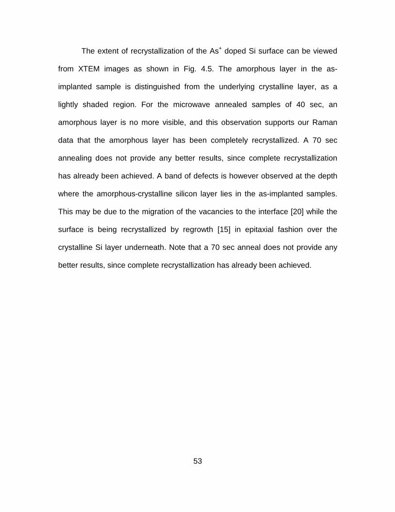
The extent of recrystallization of the As+ doped Si surface can be viewed
from XTEM images as shown in Fig. 4.5. The amorphous layer in the as-
implanted sample is distinguished from the underlying crystalline layer, as a
lightly shaded region. For the microwave annealed samples of 40 sec, an
amorphous layer is no more visible, and this observation supports our Raman
data that the amorphous layer has been completely recrystallized. A 70 sec
annealing does not provide any better results, since complete recrystallization
has already been achieved. A band of defects is however observed at the depth
where the amorphous-crystalline silicon layer lies in the as-implanted samples.
This may be due to the migration of the vacancies to the interface [20] while the
surface is being recrystallized by regrowth [15] in epitaxial fashion over the
crystalline Si layer underneath. Note that a 70 sec anneal does not provide any
better results, since complete recrystallization has already been achieved.
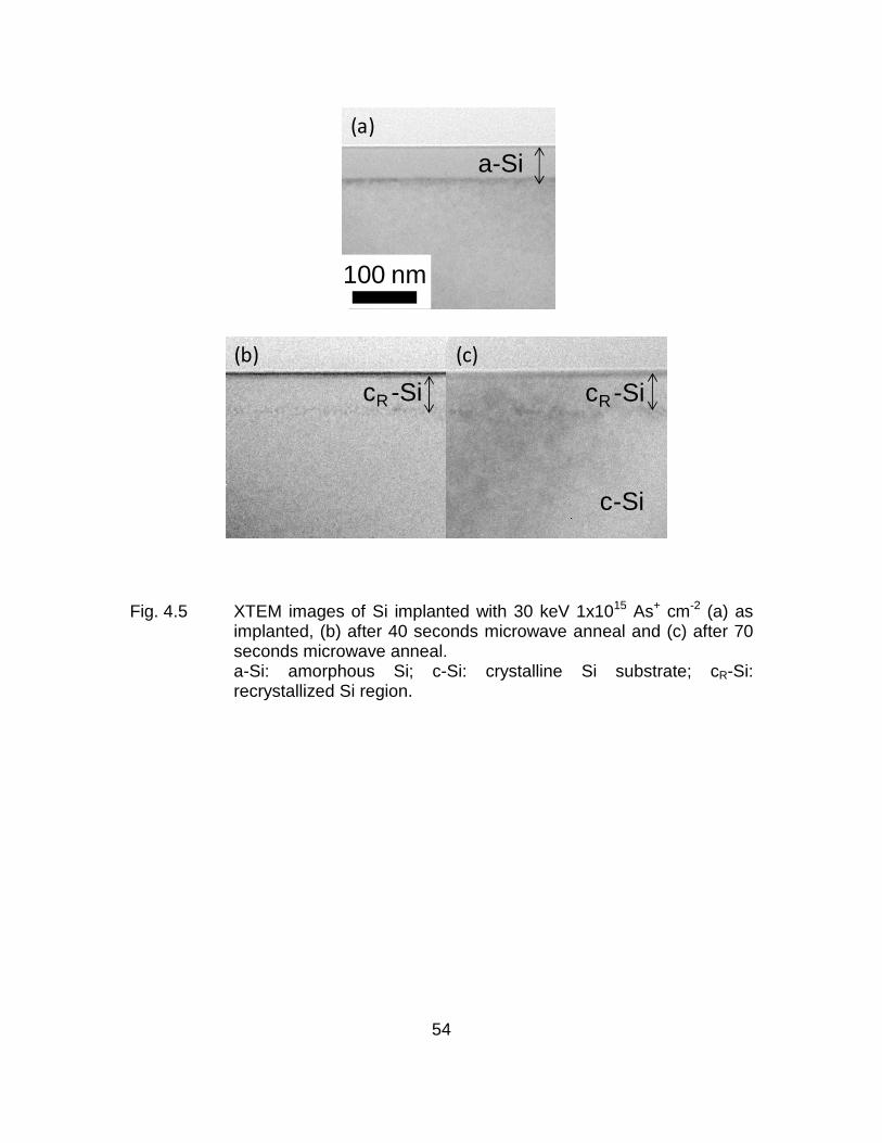
54
Fig. 4.5 XTEM images of Si implanted with 30 keV 1x10¹⁵ As+ cm-2 (a) as implanted, (b) after 40 seconds microwave anneal and (c) after 70 seconds microwave anneal. a-Si: amorphous Si; c-Si: crystalline Si substrate; cR-Si: recrystallized Si region.
(a)
a-Si
100 nm
(b) (c)
cR -Si cR -Si
c-Si
55
4.4. Discussion
Typically, a surface layer goes through incubation, before it can
recrystallize due to regrowth from an underlying crystalline layer [49].
Microwaves are capable of reducing the incubation time required, hence
achieving SPE in much lesser time. The advantage that microwave annealing
possesses over conventional annealing is that the low temperature, which is
achievable in a few seconds time (40 s in our current study), suffices for
nucleation. Previous research to explore the application of microwaves shows
that the interaction of the radiation with the atoms enhances diffusion properties
[50] of the material. The increased diffusivity of the Silicon atoms not only
provides recrystallization, but does this in a single phase, producing a single
crystal from the amorphized layer [51] that has been affirmed by our Raman
spectra results where the only peak observed other than a broad peak at 480cm -
1, is at 520cm -1 which is that of a single crystalline layer. The temperature of
about 620 oC appears to be the key factor responsible for damage repair, but it is
not enough to remove the defect bands after SPE.
From our XTEM images, a longer period of microwave annealing does not
suffice to remove the defect band, which could be the only drawback amongst all
of our recordings. To repair the defect network, an anneal temperature of 950 oC
is required [20]. The defect band observed is as a result of coagulation of deep
level interstitials that remain from the vacancy-interstitial annihilation [20, 52].
56
Arsenic has a tendency to form microclusters, causing interstitials to be freed,
that then form dislocations at the depth of the arsenic implant damage.
The specific heat capacity of arsenic is lower than that of silicon, making it
difficult to attain higher temperatures at even the surface level of the film to
facilitate a higher nucleation rate. In previous research regarding microwave
annealing of boron implanted Si wafers, nucleation was achieved without a
susceptor, although the boron atoms had a high CP of 1107 J/Kg-K, due to a low
atomic mass of the atom and hence a much lower mCP factor than Si, the power
absorbed from the microwave radiation was sufficient to provide increased local
temperatures, and hence greater rate of solid phase epitaxy equal to 2RP [20].
However, the rate of solid phase epitaxial regrowth due to conventional heating
methods [53] is given by
v ≈ ∆gca.δ exp(-Ea/kT)
h (1)
where ∆gca , the free energy difference between the crystalline and amorphous
phases is less than kT, δ is the distance across the interface between the two
phases, and Ea is the activation energy responsible for SPE. But for arsenic
implanted Si samples, high dielectric material needs to be included in the heating
setup, which allows surface heating and not volumetric heating when absorbing
microwave radiation. Surface heating causes a low DP for the susceptor, which is
57
a SiC cylinder that was filed at the mounting surface to ensure the sample placed
over it had maximum surface area contact. The sample was then placed face up
over the flat surface of the susceptor. This promotes the nucleation of the
crystalline phase upwards at the interface through the amorphous layer of the
film, because of the high upward flux of heat [54] from the susceptor. The upward
heat flux of this high temperature, then increases the local temperature of arsenic
atoms at the interface of crystalline and amorphous silicon, and provides a higher
nucleation rate to the sites, just as the metal impurities do in the MIC annealing
method. Equation 1 gives a lesser SPE rate compared to nucleating rate of twice
the projected implant range i.e., 2RP [55, 56] achieved by microwave annealing,
making the latter preferable.
4.5. Conclusion
The susceptor is not only successful in providing the advantage of higher
temperature and higher SPE growth velocity, but it does so without the addition
of metal impurities into the samples. The rate of regrowth is also much higher
compared to regular regrowth method. The studies suggest that the susceptor
assisted microwave annealing can be a suitable alternative post implantation
processing technique with improvements on magnetron used in the microwave
cavity and further care in choosing the ambient.
58
Chapter 5
KINETIC STRESS TESTING AND INFLUENCE OF LONG TIME ANNEALS ON
THE BEHAVIOR OF IZO TFTs
5.1. Introduction
Metal oxides such as ZnO have gained attention over past few years in
conductive device applications and transparent electronics. Furthermore, mixed
oxides like indium-zinc oxide and indium-gallium-zinc oxide have been explored
as alternatives to the amorphous Si active layers in thin film transistors. Owing to
the promising optical properties along with high mobilities, fabrication of
transparent electronics has become a research area that has garnered the
interest of many scientists. As a result of the mechanical stability of the mixed
oxide based structures, devices have been successfully incorporated onto
flexible substrates. To enable fabrication of TFTs on flexible substrates, the
processing temperatures are required to be low which result in increased defect
densities within the bandgap. Regardless of the mechanical stability, higher
defect density could lead to degraded performance of the devices. Extensive
work has been done to investigate the instability in ZnO based TFTs [57-61]. At
higher operational temperatures, these defects can be thermally activated and
alter the device characteristics [62]. This is an important effect that needs to be
considered in industry applications of the TFTs, since large area electronics can
generate considerable heat within the device due to dissipation of power over a
continued period of time.
59
In this study, we have performed standalone gate bias and elevated
substrate temperature stressing, and combined elevated-temperature bias stress
testing for 104 seconds. Temperatures considered to observe thermally activated
defect behavior are 20, 50, and 80 °C. The elevated temperature electrical stress
testing or kinetic stress testing elucidates the failure of the device, and the
defects responsible for the subthreshold slope changes, threshold voltage shifts,
and the dip and kink behavior of the device characteristics. The phenomenon of
the devices demonstrating two current trends beyond the on voltage region is
defined as a kink for convenience throughout this study.
Several post processing techniques have been suggested to combat the
issue of the increased defect densities in TFTs [63-64]. Anneals at temperatures
greater than 200 °C have been performed for shorter durations (as little as 30
minutes) to cure defects created during fabrication. But TFTs that have been
fabricated over flexible substrates or structures that have an encapsulation layer
over the active channel layer cannot be annealed at such high temperatures.
Furthermore, crystallization of the channel is usually achieved at higher
temperatures and does not provide benefits over the unannealed amorphous
metal oxide active layer in terms of mobilities or stability. Previous high
temperature anneal studies have shown that recrystallization can decrease the
mobility in the active channel layer [65]. A low temperature, long hour anneal has
been suggested as an alternative post process technique to cure the defects
created during low temperature fabrication [66]. The samples have been
60
annealed at 150 °C for 12, 24, 36, 48, and 60 hours , and tested for 104 seconds
under bias-only and elevated temperature electrical stress conditions. This study
further details the endurance of the TFTs to extreme stress conditions before and
after low temperature long time anneals and suggests optimum anneal conditions
under which defect density can be minimized.
5.2. Experimental Details
The cross section of the bottom gate staggered structure IZO TFTs tested
in this study can be seen in Fig. 5.1(a). The TFTs have been fabricated at 180 °C
on a 300 mm Si wafer. Molybdenum has been used as the gate metal and is
deposited onto the substrate by sputtering. After patterning of the gate, the gate
dielectric SiO2 is deposited at 180 °C using plasma enhanced chemi cal vapor
deposition at power density of 0.43 W/cm2 and a pressure of 1.5 Torr. This is
followed by deposition of 50 nm thick channel layer (IZO) from a target of In:Zn
ratio of 40:60, by sputtering at RF power of 300 W and pressure of 16 mTorr. The
gas ratio used for channel layer deposition was 1:50 parts oxygen with argon gas
(3.7 sccm O2: 185 sccm Ar). Another layer of SiO is deposited to form the
passivation layer. SiO deposited using afore mentioned conditions also forms the
etch stopper. The gate oxide, channel layer, and passivation layer are patterned
using photolithography for source/drain metal deposition. Finally, Mo is sputtered
and etched using an AMAT 8330 dry etcher to form source/drain electrodes. The
W/L of devices is 110/11.
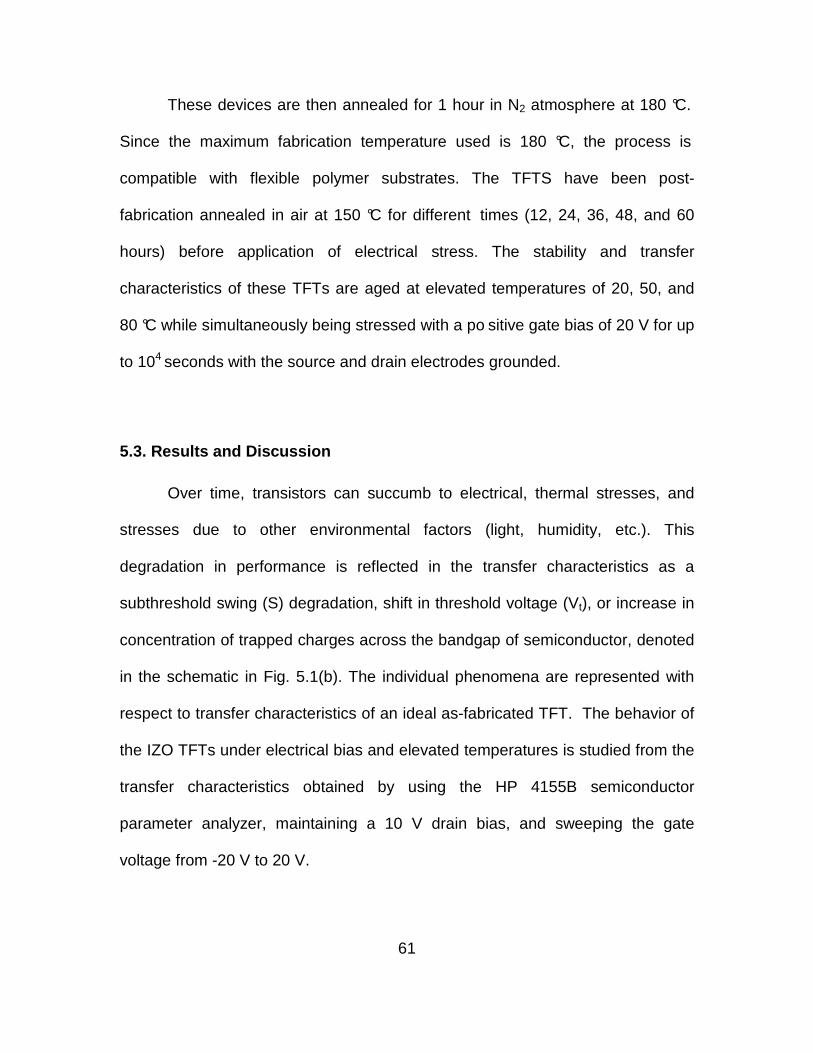
61
These devices are then annealed for 1 hour in N2 atmosphere at 180 °C.
Since the maximum fabrication temperature used is 180 °C, the process is
compatible with flexible polymer substrates. The TFTS have been post-
fabrication annealed in air at 150 °C for different times (12, 24, 36, 48, and 60
hours) before application of electrical stress. The stability and transfer
characteristics of these TFTs are aged at elevated temperatures of 20, 50, and
80 °C while simultaneously being stressed with a po sitive gate bias of 20 V for up
to 104 seconds with the source and drain electrodes grounded.
5.3. Results and Discussion
Over time, transistors can succumb to electrical, thermal stresses, and
stresses due to other environmental factors (light, humidity, etc.). This
degradation in performance is reflected in the transfer characteristics as a
subthreshold swing (S) degradation, shift in threshold voltage (Vt), or increase in
concentration of trapped charges across the bandgap of semiconductor, denoted
in the schematic in Fig. 5.1(b). The individual phenomena are represented with
respect to transfer characteristics of an ideal as-fabricated TFT. The behavior of
the IZO TFTs under electrical bias and elevated temperatures is studied from the
transfer characteristics obtained by using the HP 4155B semiconductor
parameter analyzer, maintaining a 10 V drain bias, and sweeping the gate
voltage from -20 V to 20 V.
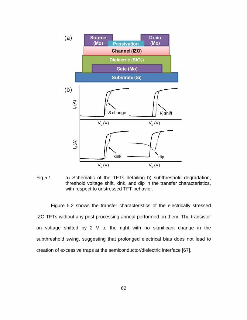
62
Fig 5.1 a) Schematic of the TFTs detailing b) subthreshold degradation,
threshold voltage shift, kink, and dip in the transfer characteristics, with respect to unstressed TFT behavior.
Figure 5.2 shows the transfer characteristics of the electrically stressed
IZO TFTs without any post-processing anneal performed on them. The transistor
on voltage shifted by 2 V to the right with no significant change in the
subthreshold swing, suggesting that prolonged electrical bias does not lead to
creation of excessive traps at the semiconductor/dielectric interface [67].
63
Fig. 5.2 Transfer characteristics of the as-fabricated TFT under 10,000 seconds of 20 V gate stress.
In order to understand the effect of electrical bias at elevated
temperatures, the substrates were subjected to heating for 104 seconds at 50 and
80 °C, with the field effect mobilities and the sub threshold swings demonstrating
minor variations. The onset of device degradation was determined by the
instability in the off region of the transistors as seen in Fig. 5.3. The phenomenon
depicted in Fig. 5.3 is thermally assisted; where with time, the number of carriers
that are contributed by electron-hole pairs increase (~ 3,000 seconds for a 50 °C
heat treatment), increasing the off currents to orders of 10-7 A. Thermally excited
holes from the trap states tend to accumulate near the source region over time,
and reduce the barrier for hole and electron transport at the source-channel
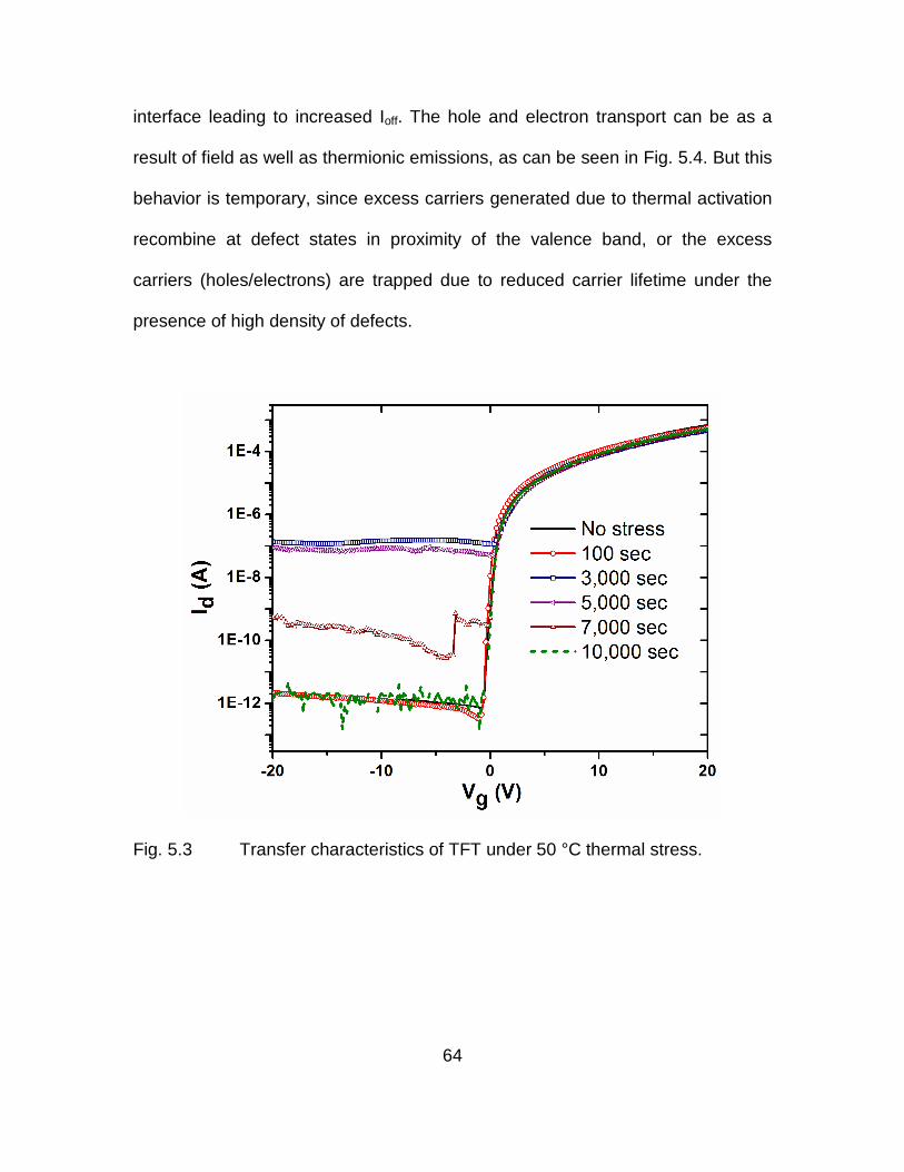
64
interface leading to increased Ioff. The hole and electron transport can be as a
result of field as well as thermionic emissions, as can be seen in Fig. 5.4. But this
behavior is temporary, since excess carriers generated due to thermal activation
recombine at defect states in proximity of the valence band, or the excess
carriers (holes/electrons) are trapped due to reduced carrier lifetime under the
presence of high density of defects.
Fig. 5.3 Transfer characteristics of TFT under 50 °C thermal stress.
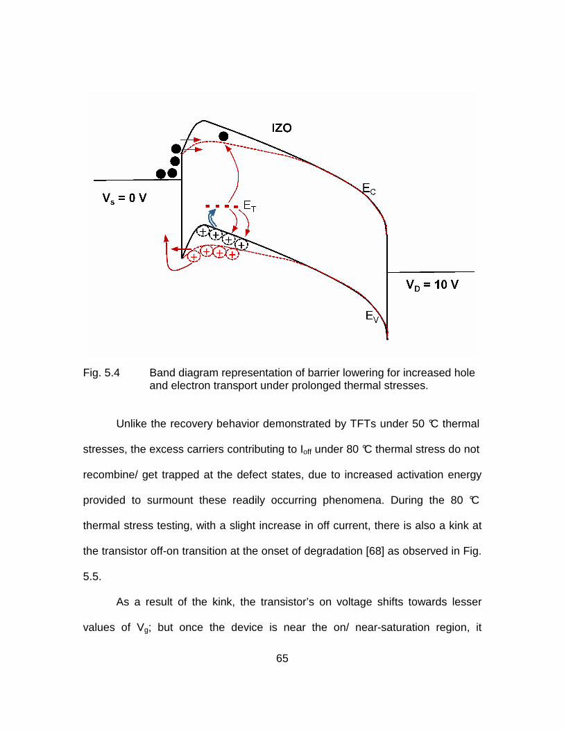
65
Fig. 5.4 Band diagram representation of barrier lowering for increased hole and electron transport under prolonged thermal stresses.
Unlike the recovery behavior demonstrated by TFTs under 50 °C thermal
stresses, the excess carriers contributing to Ioff under 80 °C thermal stress do not
recombine/ get trapped at the defect states, due to increased activation energy
provided to surmount these readily occurring phenomena. During the 80 °C
thermal stress testing, with a slight increase in off current, there is also a kink at
the transistor off-on transition at the onset of degradation [68] as observed in Fig.
5.5.
As a result of the kink, the transistor’s on voltage shifts towards lesser
values of Vg; but once the device is near the on/ near-saturation region, it
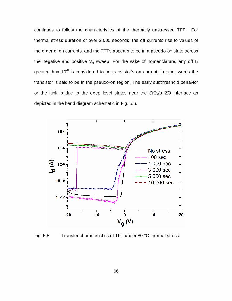
66
continues to follow the characteristics of the thermally unstressed TFT. For
thermal stress duration of over 2,000 seconds, the off currents rise to values of
the order of on currents, and the TFTs appears to be in a pseudo-on state across
the negative and positive Vg sweep. For the sake of nomenclature, any off Id
greater than 10-8 is considered to be transistor’s on current, in other words the
transistor is said to be in the pseudo-on region. The early subthreshold behavior
or the kink is due to the deep level states near the SiOx/a-IZO interface as
depicted in the band diagram schematic in Fig. 5.6.
Fig. 5.5 Transfer characteristics of TFT under 80 °C thermal stress.
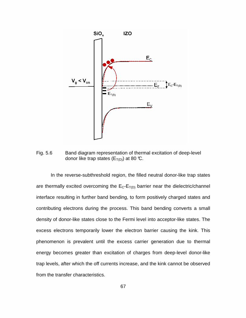
67
Fig. 5.6 Band diagram representation of thermal excitation of deep-level donor like trap states (ET(D)) at 80 °C.
In the reverse-subthreshold region, the filled neutral donor-like trap states
are thermally excited overcoming the EC-ET(D) barrier near the dielectric/channel
interface resulting in further band bending, to form positively charged states and
contributing electrons during the process. This band bending converts a small
density of donor-like states close to the Fermi level into acceptor-like states. The
excess electrons temporarily lower the electron barrier causing the kink. This
phenomenon is prevalent until the excess carrier generation due to thermal
energy becomes greater than excitation of charges from deep-level donor-like
trap levels, after which the off currents increase, and the kink cannot be observed
from the transfer characteristics.
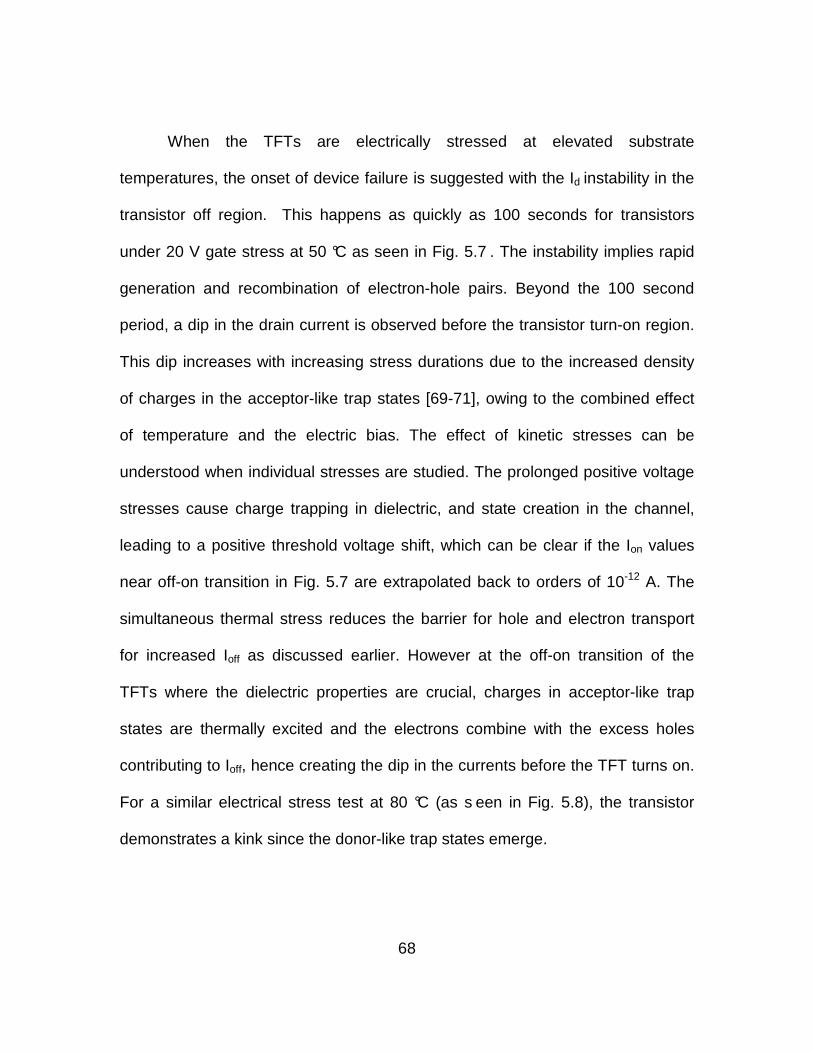
68
When the TFTs are electrically stressed at elevated substrate
temperatures, the onset of device failure is suggested with the Id instability in the
transistor off region. This happens as quickly as 100 seconds for transistors
under 20 V gate stress at 50 °C as seen in Fig. 5.7 . The instability implies rapid
generation and recombination of electron-hole pairs. Beyond the 100 second
period, a dip in the drain current is observed before the transistor turn-on region.
This dip increases with increasing stress durations due to the increased density
of charges in the acceptor-like trap states [69-71], owing to the combined effect
of temperature and the electric bias. The effect of kinetic stresses can be
understood when individual stresses are studied. The prolonged positive voltage
stresses cause charge trapping in dielectric, and state creation in the channel,
leading to a positive threshold voltage shift, which can be clear if the Ion values
near off-on transition in Fig. 5.7 are extrapolated back to orders of 10-12 A. The
simultaneous thermal stress reduces the barrier for hole and electron transport
for increased Ioff as discussed earlier. However at the off-on transition of the
TFTs where the dielectric properties are crucial, charges in acceptor-like trap
states are thermally excited and the electrons combine with the excess holes
contributing to Ioff, hence creating the dip in the currents before the TFT turns on.
For a similar electrical stress test at 80 °C (as s een in Fig. 5.8), the transistor
demonstrates a kink since the donor-like trap states emerge.
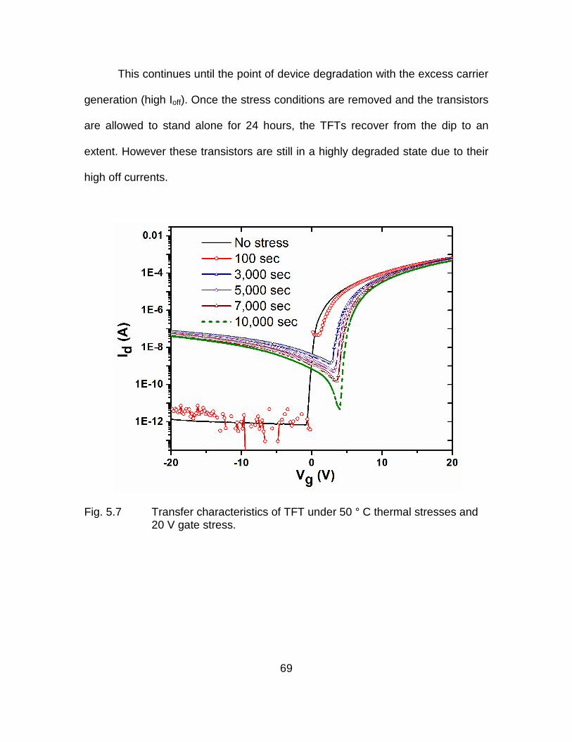
69
This continues until the point of device degradation with the excess carrier
generation (high Ioff). Once the stress conditions are removed and the transistors
are allowed to stand alone for 24 hours, the TFTs recover from the dip to an
extent. However these transistors are still in a highly degraded state due to their
high off currents.
Fig. 5.7 Transfer characteristics of TFT under 50 ° C thermal stresses and 20 V gate stress.
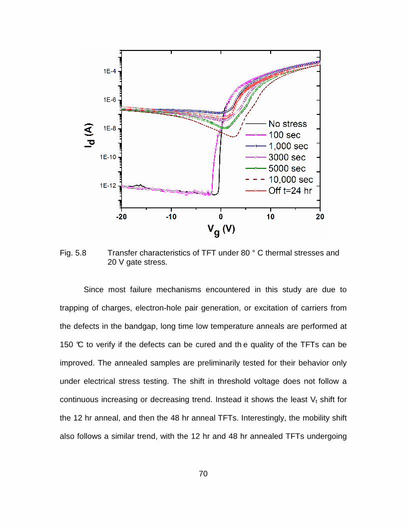
70
Fig. 5.8 Transfer characteristics of TFT under 80 ° C thermal stresses and 20 V gate stress.
Since most failure mechanisms encountered in this study are due to
trapping of charges, electron-hole pair generation, or excitation of carriers from
the defects in the bandgap, long time low temperature anneals are performed at
150 °C to verify if the defects can be cured and th e quality of the TFTs can be
improved. The annealed samples are preliminarily tested for their behavior only
under electrical stress testing. The shift in threshold voltage does not follow a
continuous increasing or decreasing trend. Instead it shows the least Vt shift for
the 12 hr anneal, and then the 48 hr anneal TFTs. Interestingly, the mobility shift
also follows a similar trend, with the 12 hr and 48 hr annealed TFTs undergoing
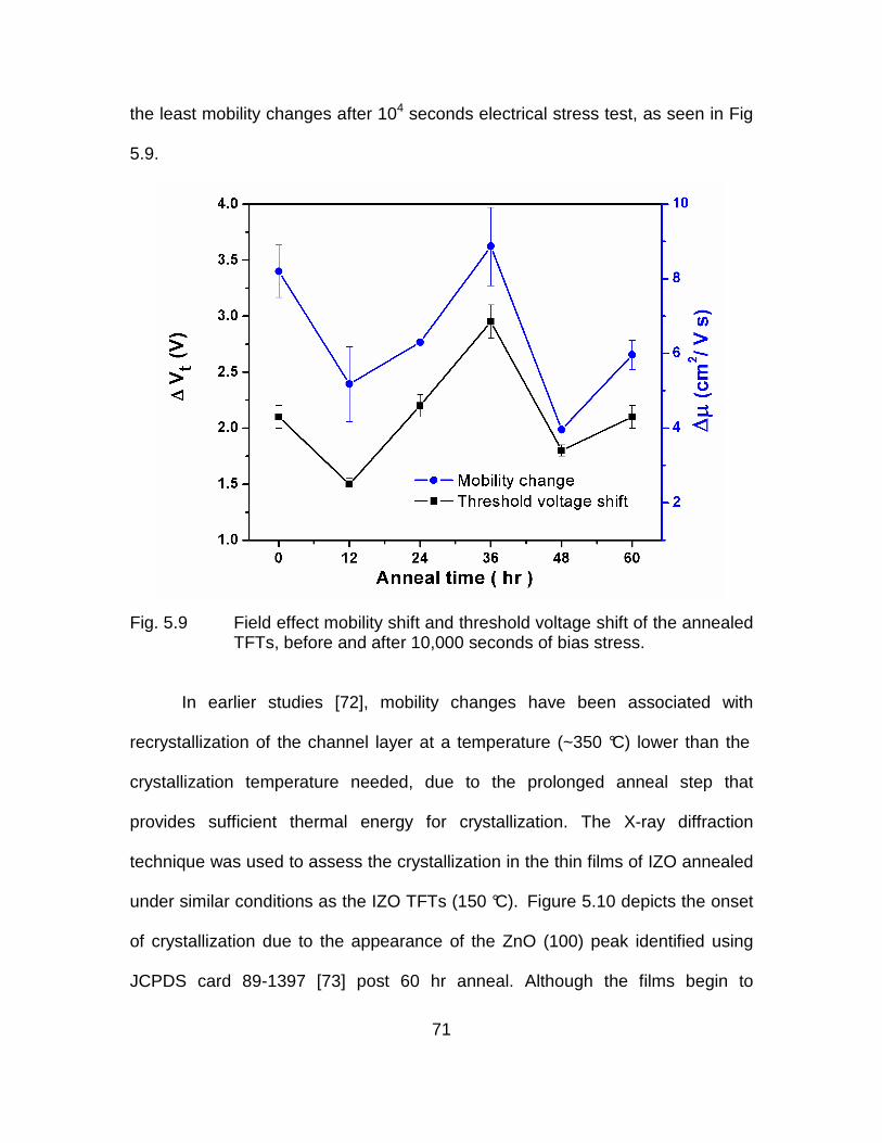
71
the least mobility changes after 104 seconds electrical stress test, as seen in Fig
5.9.
Fig. 5.9 Field effect mobility shift and threshold voltage shift of the annealed TFTs, before and after 10,000 seconds of bias stress.
In earlier studies [72], mobility changes have been associated with
recrystallization of the channel layer at a temperature (~350 °C) lower than the
crystallization temperature needed, due to the prolonged anneal step that
provides sufficient thermal energy for crystallization. The X-ray diffraction
technique was used to assess the crystallization in the thin films of IZO annealed
under similar conditions as the IZO TFTs (150 °C). Figure 5.10 depicts the onset
of crystallization due to the appearance of the ZnO (100) peak identified using
JCPDS card 89-1397 [73] post 60 hr anneal. Although the films begin to
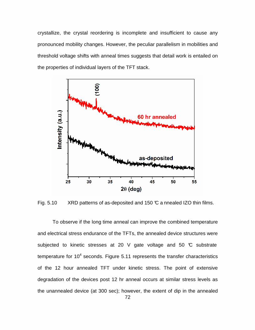
72
crystallize, the crystal reordering is incomplete and insufficient to cause any
pronounced mobility changes. However, the peculiar parallelism in mobilities and
threshold voltage shifts with anneal times suggests that detail work is entailed on
the properties of individual layers of the TFT stack.
Fig. 5.10 XRD patterns of as-deposited and 150 °C a nnealed IZO thin films.
To observe if the long time anneal can improve the combined temperature
and electrical stress endurance of the TFTs, the annealed device structures were
subjected to kinetic stresses at 20 V gate voltage and 50 °C substrate
temperature for 104 seconds. Figure 5.11 represents the transfer characteristics
of the 12 hour annealed TFT under kinetic stress. The point of extensive
degradation of the devices post 12 hr anneal occurs at similar stress levels as
the unannealed device (at 300 sec); however, the extent of dip in the annealed
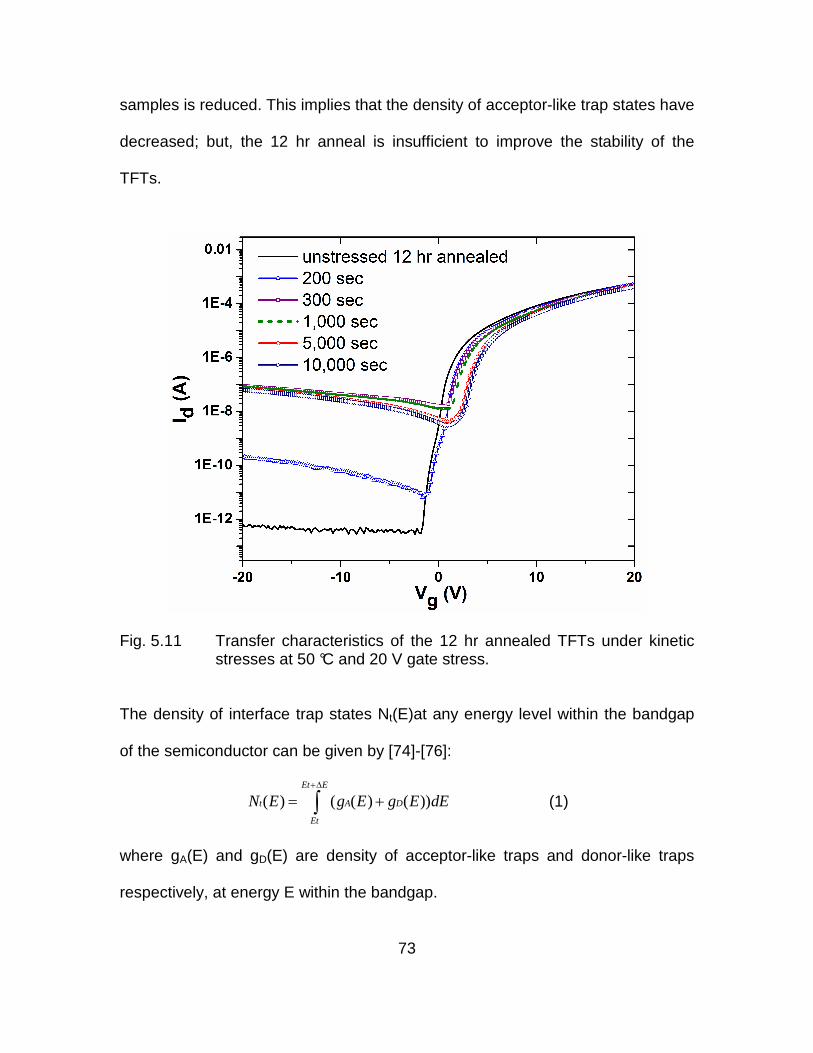
73
samples is reduced. This implies that the density of acceptor-like trap states have
decreased; but, the 12 hr anneal is insufficient to improve the stability of the
TFTs.
Fig. 5.11 Transfer characteristics of the 12 hr annealed TFTs under kinetic stresses at 50 °C and 20 V gate stress.
The density of interface trap states Nt(E)at any energy level within the bandgap
of the semiconductor can be given by [74]-[76]:
( ) ( ( ) ( ))Et E
t A D
Et
N E g E g E dE+∆
= +∫ (1)
where gA(E) and gD(E) are density of acceptor-like traps and donor-like traps
respectively, at energy E within the bandgap.
74
The charges trapped in acceptor-like states near the transistor threshold region
are greater in concentration than the charges trapped in donor-like states, due to
the dip in the on current. Hence, relation (1) can be rewritten as [77,78]
1( ) ( ) ( )Et E
t A ta
Et
N E g E dE N f E+∆
≅ = ×∫ (2)
where taN is the total density of acceptor-like traps, and 1( )f E is a Gaussian or
exponential function representing ( )tN E as a function of peak energy of states
and energy E. The total density of trapped charges, tN , in the bandgap can be
obtained by integrating the expression (2) over the entire bandgap [79]:
1
( ) ( )
( ) ( )
Ec
t t
Ev
Ec
ta
Ev
N N E f E dE
N f E f E dE
= ×
= × ×
∫
∫ (3)
where ( )f E is the probability of a trap state being occupied.
The acceptor-like trapped charges influence the transistor on current (see
Appendix for derivation) as follows [80-82]:
( )/d d
ox 0 Bg
3 2t
Bg ox
I V=W C µ exp -E kT
V L
q N tE
8 V C
=∈
(4)
where the value of d
g
I
Vcan be obtained from the transfer characteristics, and is
proportional to the exponential prefactor in equation (4). When the data from
Figs. 7 and 11 is modeled to fit the equation (4), the slope of the relation between
75
d
g
Ilog
e V
and 1
gV
indicates that the density of trap states have reduced by a
factor of 0.42 (Nt (12 hr anneal) = 0.42 × Nt (unanneled)) post 12 hr anneal, i.e., tN drops
by 58 %.
The 24, 36, 48, and 60 hr annealed samples are tested similarly; however
only the TFTs annealed beyond 48 hours demonstrate considerable stability,
while the 24 and 36 hr annealed structures fail over a certain period of stress. As
seen in Fig. 12, the 48 hr annealed device did not undergo failure (from high Ioff)
even after 104 seconds of kinetic stress test. The on/off Id ratio only drops from
5×10⁸ to 5×10⁷ with reduced kink for increasing stress times when compared to a
degraded on-off ratio of around 104. The density of acceptor-like traps cannot be
discerned from Fig. 5.12 due to the absence of a dip in the transfer
characteristics which suggests that the 48 hr anneal has reduced the
concentration of charges in acceptor-like states, and by extension the density of
acceptor-like states itself, significantly. The TFTs annealed for 60 hr (not shown)
reveal a superior performance from the 48 hr annealed devices, confirmed by an
absence of dip and kink phenomena under kinetic stress tests. This enhanced
stability at an elevated temperature suggests that the density of defects that can
be excited due to thermal activation has been substantially reduced.
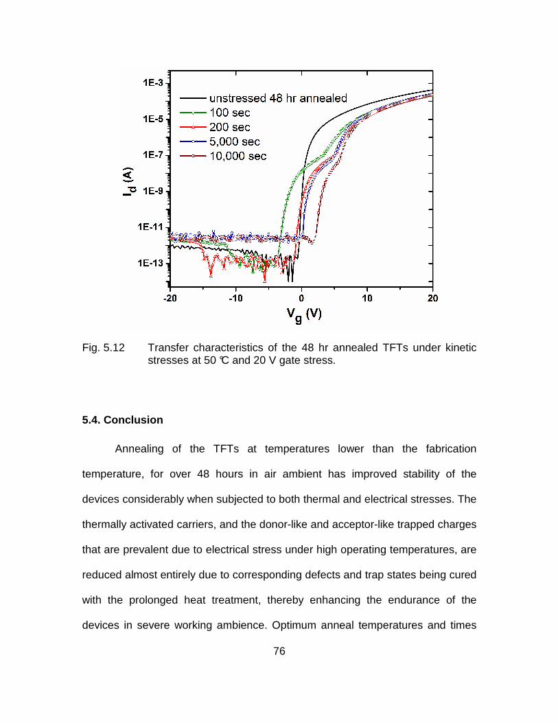
76
Fig. 5.12 Transfer characteristics of the 48 hr annealed TFTs under kinetic stresses at 50 °C and 20 V gate stress.
5.4. Conclusion
Annealing of the TFTs at temperatures lower than the fabrication
temperature, for over 48 hours in air ambient has improved stability of the
devices considerably when subjected to both thermal and electrical stresses. The
thermally activated carriers, and the donor-like and acceptor-like trapped charges
that are prevalent due to electrical stress under high operating temperatures, are
reduced almost entirely due to corresponding defects and trap states being cured
with the prolonged heat treatment, thereby enhancing the endurance of the
devices in severe working ambience. Optimum anneal temperatures and times
77
have been chosen to cure the defects rampant from the low temperature
fabrication, without crystallizing the channel. This is a preferable outcome, since
amorphous metal oxides possess better semiconducting properties as channel
materials than crystalline metal oxides. The 48 hr annealed samples have also
demonstrated the best mobility stability and threshold voltage stability when
subjected to a 20 V gate bias, second to the 12 hr annealed devices. However,
the 12 hr anneals are inadequate to stabilize the TFT performance under thermal
stress. The onset of reliable device behavior is observed for TFTs annealed for
over 48 hours. This study also elucidates the phenomena responsible for the
threshold shift, the kink, and the dip in the device characteristics to gather a
better understanding of the measures necessary to address the type of defects
responsible effectively.
5.5. Appendix
As mentioned earlier, in amorphous or poly-crystalline materials, there is
an increased density of defects within the bandgap that can be excited to
contribute towards excess carriers. Following the thermionic theory of current the
mobility in amorphous channel material can be expressed as:
( )/0 aµ = µ exp -E kT
The activation energy for carriers/donors within the bandgap (Ea), can be
approximated as the barrier height for defects (EB). The drain current for TFTs in
the linear region is given as:

78
dd 0 g ox
VI µ W V C
L=
, which for amorphous materials is:
( )/d d
ox 0 Bg
I V=W C µ exp -E kT
V L
The barrier height of the defects at the interface is derived as [80, 81]:
G
2 2t
Bq N
E8 N
=∈
NG is the gate induced charge concentration per area, as a result of the positive
gate voltage which reduces barrier to interface states, essentially contributing
donors to the conduction. Hence:
G
G
V
q
oxCN
t =
The drain current for amorphous channel based TFTs can therefore be written
as:
( )/d d
ox 0 Bg
I V=W C µ exp -E kT
V L
where 3 2
tB
g ox
q N tE
8 V C=
∈
79
Chapter 6
INVESTIGATION OF DEFECT GENERATION AND ANNIHILATION IN IGZO
TFTs DURING PRACTICAL STRESS CONDITIONS: ILLUMINATION AND
ELECTRICAL BIAS
6.1. Introduction
Metal-oxide based thin film transistors (TFTs) fabricated at low
temperatures are an attractive replacement for previous generation a-Si:H TFTs
due to their higher mobilities and improved optical transparency in the visible
region. But before they can supplant other well developed a-Si:H based active
electronics, extensive research on the stability of the amorphous metal oxide
transistors is necessary. Although bias stress testing provides knowledge of
factors that may alter the characteristics of the transistors, failure and stability
tests are incomplete without taking into consideration the impact of different
wavelengths of light (which are an integral part of the active backlight of any
display electronics [70,83,84]) that drastically drive the transistors into failure
upon continuous illumination. TFTs based on a-Si:H active regions have been
used in back-panels of LCD technology extensively; however, this technology
needs replacement due to threshold voltage instability upon bias stress of only a
few hours [85, 60]. Metal-oxide based active channel regions have been
suggested for the fabrication of TFTs and have shown much better threshold
voltage stability under both positive and negative bias stresses [60]. However the
effects of photo-induced phenomena on the TFTs have not been studied in
80
detail. This is especially necessary since the metal-oxide TFTs are found to have
an application in transparent thin film devices owing to their optical transparency
in the visible region of the light spectrum. Several researchers have tried to study
the effect of UV radiation [25, 86-90], but stability testing in real-life applications
would have to consider wavelengths in the visible spectrum. In this study, we
have exhaustively investigated instability in mixed oxide based TFTs due to bias
stress, illumination, and the combination of both.
6.2. Experimental Procedure
IGZO TFTs were fabricated as bottom gate staggered n-type
enhancement mode devices with the cross-section shown in Fig. 6.1. The
substrate used is a 300 mm silicon wafer with a thin layer of SiN. The gate metal
is 150 nm thick molybdenum and is deposited using a sputtering process in a DC
sputter system. After patterning the gate layer, a stack of SiOx, IGZO, and SiOx is
deposited in series. A 200 nm silicon oxide deposited layer forms the gate
dielectric. The 50 nm thick channel material IGZO with 99.99% pure InGaZnO4 is
deposited at an RF power of 100 W and a chamber pressure of 10 mTorr at 80
°C and a 100 nm intermetal dielectric (IMD) SiO x is deposited at 180 oC. The
IGZO layer is patterned and the source–drain metal (moly) is sputtered to form
the source and drain contacts of the TFT. A final step involves deposition of SiN,
to act as a passivation layer. After the etch step, called the overglass etching
process, the entire wafer is annealed at 200 °C for 1 hour and this is the
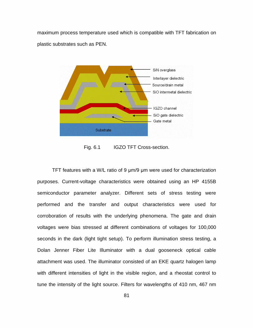
81
maximum process temperature used which is compatible with TFT fabrication on
plastic substrates such as PEN.
Fig. 6.1 IGZO TFT Cross-section.
TFT features with a W/L ratio of 9 µm/9 µm were used for characterization
purposes. Current-voltage characteristics were obtained using an HP 4155B
semiconductor parameter analyzer. Different sets of stress testing were
performed and the transfer and output characteristics were used for
corroboration of results with the underlying phenomena. The gate and drain
voltages were bias stressed at different combinations of voltages for 100,000
seconds in the dark (light tight setup). To perform illumination stress testing, a
Dolan Jenner Fiber Lite Illuminator with a dual gooseneck optical cable
attachment was used. The illuminator consisted of an EKE quartz halogen lamp
with different intensities of light in the visible region, and a rheostat control to
tune the intensity of the light source. Filters for wavelengths of 410 nm, 467 nm
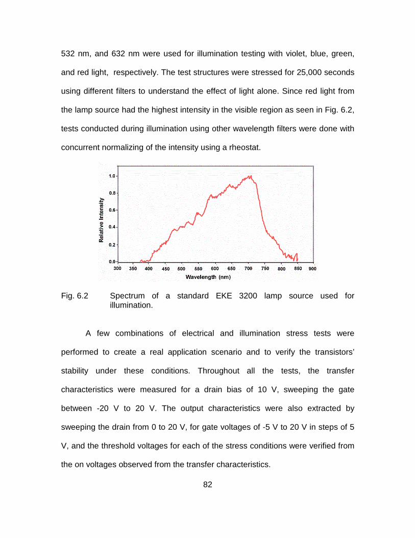
82
532 nm, and 632 nm were used for illumination testing with violet, blue, green,
and red light, respectively. The test structures were stressed for 25,000 seconds
using different filters to understand the effect of light alone. Since red light from
the lamp source had the highest intensity in the visible region as seen in Fig. 6.2,
tests conducted during illumination using other wavelength filters were done with
concurrent normalizing of the intensity using a rheostat.
Fig. 6.2 Spectrum of a standard EKE 3200 lamp source used for illumination.
A few combinations of electrical and illumination stress tests were
performed to create a real application scenario and to verify the transistors’
stability under these conditions. Throughout all the tests, the transfer
characteristics were measured for a drain bias of 10 V, sweeping the gate
between -20 V to 20 V. The output characteristics were also extracted by
sweeping the drain from 0 to 20 V, for gate voltages of -5 V to 20 V in steps of 5
V, and the threshold voltages for each of the stress conditions were verified from
the on voltages observed from the transfer characteristics.
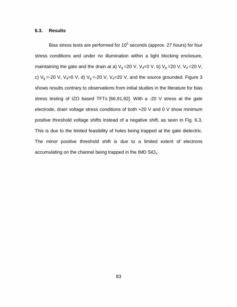
83
6.3. Results
Bias stress tests are performed for 105 seconds (approx. 27 hours) for four
stress conditions and under no illumination within a light blocking enclosure,
maintaining the gate and the drain at a) Vg =20 V, Vd=0 V, b) Vg =20 V, Vd =20 V,
c) Vg =-20 V, Vd=0 V, d) Vg =-20 V, Vd=20 V, and the source grounded. Figure 3
shows results contrary to observations from initial studies in the literature for bias
stress testing of IZO based TFTs [66,91,92]. With a -20 V stress at the gate
electrode, drain voltage stress conditions of both +20 V and 0 V show minimum
positive threshold voltage shifts instead of a negative shift, as seen in Fig. 6.3.
This is due to the limited feasibility of holes being trapped at the gate dielectric.
The minor positive threshold shift is due to a limited extent of electrons
accumulating on the channel being trapped in the IMD SiOx.
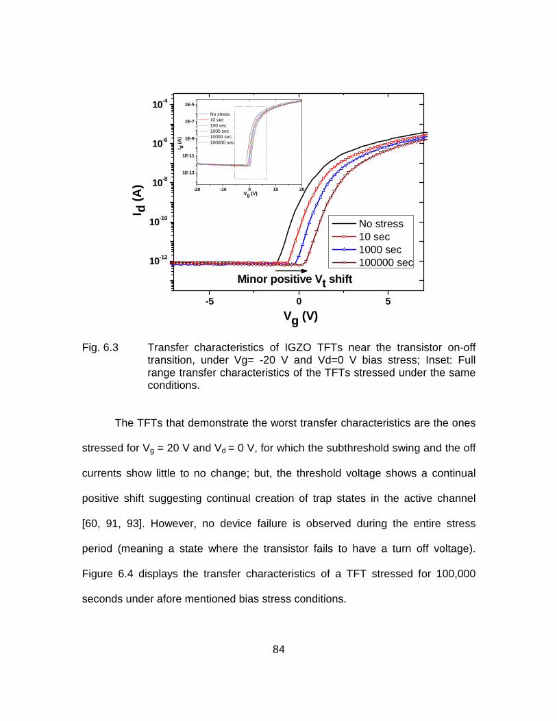
84
Fig. 6.3 Transfer characteristics of IGZO TFTs near the transistor on-off transition, under Vg= -20 V and Vd=0 V bias stress; Inset: Full range transfer characteristics of the TFTs stressed under the same conditions.
The TFTs that demonstrate the worst transfer characteristics are the ones
stressed for Vg = 20 V and Vd = 0 V, for which the subthreshold swing and the off
currents show little to no change; but, the threshold voltage shows a continual
positive shift suggesting continual creation of trap states in the active channel
[60, 91, 93]. However, no device failure is observed during the entire stress
period (meaning a state where the transistor fails to have a turn off voltage).
Figure 6.4 displays the transfer characteristics of a TFT stressed for 100,000
seconds under afore mentioned bias stress conditions.
-5 0 5
10-12
10-10
10-8
10-6
10-4
Minor positive Vt shift
I d (
A)
Vg (V)
No stress 10 sec 1000 sec 100000 sec
-20 -10 0 10 20
1E-13
1E-11
1E-9
1E-7
1E-5
I d (
A)
Vg (V)
No stress 10 sec 100 sec 1000 sec 10000 sec 100000 sec
85
Fig. 6.4 IGZO under Vg=20 V, Vd=0 V bias stress for 100,000 seconds.
Illumination stress testing with light wavelengths of 410 nm, 467 nm, 532
nm, and 632 nm for 25,000 seconds was performed with an intensity of 0.5
W/cm2. The results demonstrate a greater negative shift in threshold voltage, for
light of shorter wavelength. The 632 nm wavelength illumination results in little to
no shift in transfer characteristics that could be attributed to phenomena such as
state creation or charge trapping. As the wavelength of light used is reduced, a
considerable threshold voltage shift is noticed, making the turn on voltage
smaller, with a slight increase in mobility (see in Fig. 6.5). The shortest
wavelength light demonstrated a threshold voltage change of -17 V after 25,000
seconds. Unlike gate bias stress where there is a continual change in the
interface state density owing to higher threshold voltage, the phenomena that
-20 -10 0 10 2010-15
10-13
10-11
10-9
10-7
10-5
10-3
Large positive Vt shift
I d (
A)
Vg (V)
No Stress 10s 100s 1000s 10000s 100000s
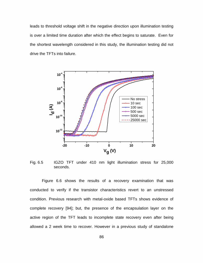
86
leads to threshold voltage shift in the negative direction upon illumination testing
is over a limited time duration after which the effect begins to saturate. Even for
the shortest wavelength considered in this study, the illumination testing did not
drive the TFTs into failure.
Fig. 6.5 IGZO TFT under 410 nm light illumination stress for 25,000 seconds.
Figure 6.6 shows the results of a recovery examination that was
conducted to verify if the transistor characteristics revert to an unstressed
condition. Previous research with metal-oxide based TFTs shows evidence of
complete recovery [94]; but, the presence of the encapsulation layer on the
active region of the TFT leads to incomplete state recovery even after being
allowed a 2 week time to recover. However in a previous study of standalone
-20 -10 0 10 20
10-12
10-10
10-8
10-6
10-4
I d (
A)
Vg (V)
No stress 10 sec 100 sec 500 sec 5000 sec 25000 sec
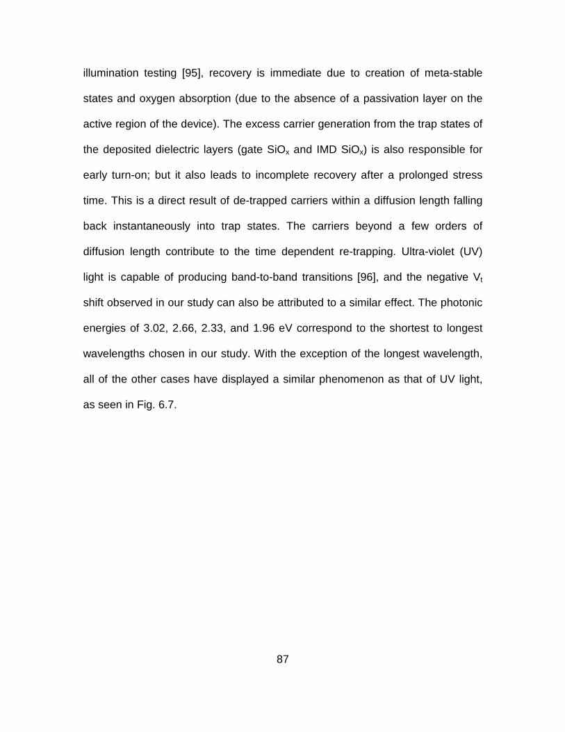
87
illumination testing [95], recovery is immediate due to creation of meta-stable
states and oxygen absorption (due to the absence of a passivation layer on the
active region of the device). The excess carrier generation from the trap states of
the deposited dielectric layers (gate SiOx and IMD SiOx) is also responsible for
early turn-on; but it also leads to incomplete recovery after a prolonged stress
time. This is a direct result of de-trapped carriers within a diffusion length falling
back instantaneously into trap states. The carriers beyond a few orders of
diffusion length contribute to the time dependent re-trapping. Ultra-violet (UV)
light is capable of producing band-to-band transitions [96], and the negative Vt
shift observed in our study can also be attributed to a similar effect. The photonic
energies of 3.02, 2.66, 2.33, and 1.96 eV correspond to the shortest to longest
wavelengths chosen in our study. With the exception of the longest wavelength,
all of the other cases have displayed a similar phenomenon as that of UV light,
as seen in Fig. 6.7.
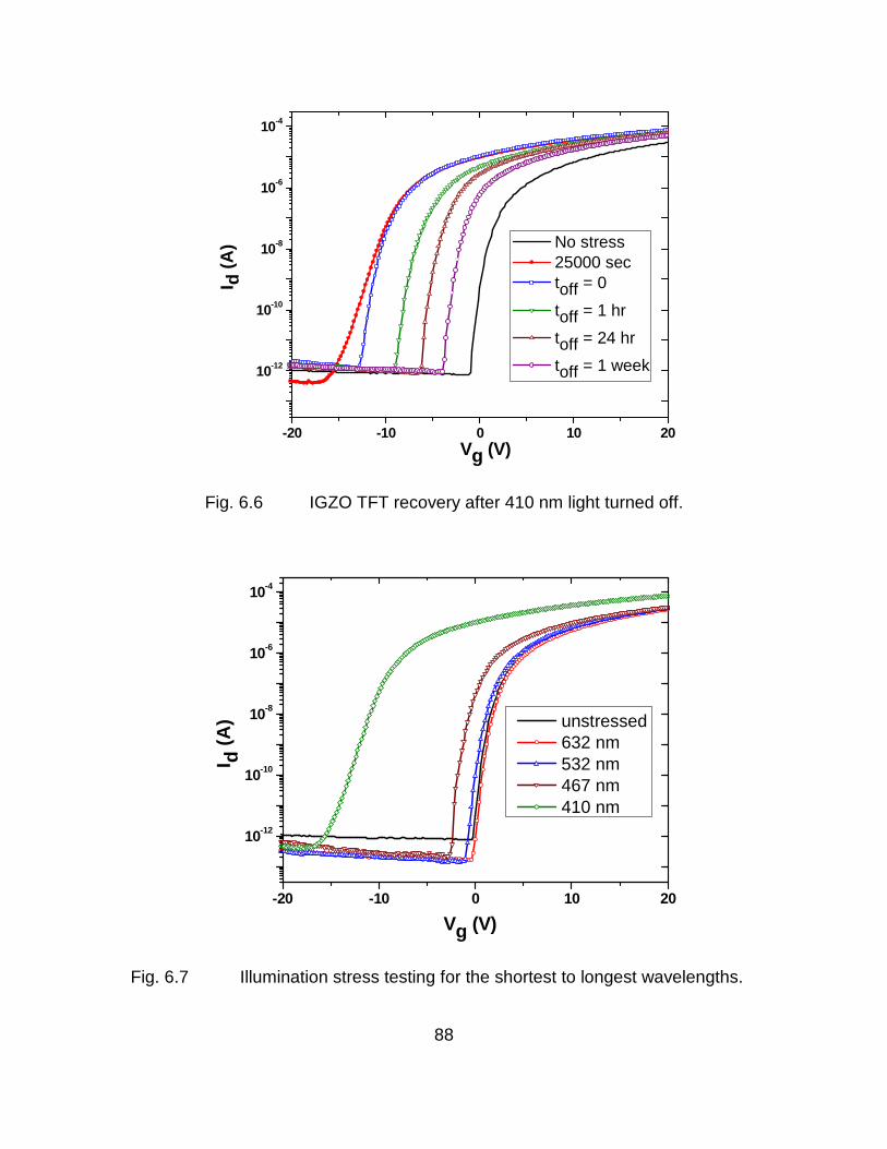
88
Fig. 6.6 IGZO TFT recovery after 410 nm light turned off.
Fig. 6.7 Illumination stress testing for the shortest to longest wavelengths.
-20 -10 0 10 20
10-12
10-10
10-8
10-6
10-4
Vg (V)
I d (
A) No stress
25000 sec toff = 0
toff = 1 hr
toff = 24 hr
toff = 1 week
-20 -10 0 10 20
10-12
10-10
10-8
10-6
10-4
I d (
A)
Vg (V)
unstressed 632 nm 532 nm 467 nm 410 nm
89
Bias stress testing has been performed in combination with extreme
wavelengths of light chosen in this study i.e., 632 nm and 410 nm. It can be
understood that 632 nm light, having no effect on the transistor characteristics,
allows the gate bias to play a dominant role in altering the transfer
characteristics. Performing the combinatorial tests with 410 nm light wavelength
with a –20 V stress on the gate electrode drives the device into failure
temporarily; where illumination and the effect of negative gate bias play an equal
role to the point that the device is in an on condition over the entire range of
voltage (see Fig. 6.8). When the light source is turned off, the device regains
functionality as a transistor with on and off voltages, but could not completely
recover to an unstressed state as discussed earlier.
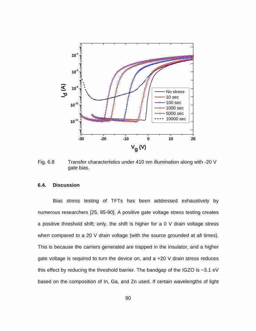
90
Fig. 6.8 Transfer characteristics under 410 nm illumination along with -20 V gate bias.
6.4. Discussion
Bias stress testing of TFTs has been addressed exhaustively by
numerous researchers [25, 85-90]. A positive gate voltage stress testing creates
a positive threshold shift; only, the shift is higher for a 0 V drain voltage stress
when compared to a 20 V drain voltage (with the source grounded at all times).
This is because the carriers generated are trapped in the insulator, and a higher
gate voltage is required to turn the device on, and a +20 V drain stress reduces
this effect by reducing the threshold barrier. The bandgap of the IGZO is ~3.1 eV
based on the composition of In, Ga, and Zn used. If certain wavelengths of light
-30 -20 -10 0 10 20
10-12
10-10
10-8
10-6
10-4
No stress 10 sec 100 sec 1000 sec 5000 sec 10000 sec
I d (
A)
Vg (V)
91
generate photonic energies greater than this bandgap, it can lead to a band to
band transition of carriers from the valence band to the conduction band and
results in an increase in net carrier concentration in the active region, and hence
a negative shift in threshold voltage. There are two theories that support the
results.
Charge carriers trapped during fabrication in the deep level traps in the
bandgap of the semiconductor and dielectric material are released to the
conduction band. This increases the net carrier concentration. Previous studies
on illumination of TFTs have shown that an increase in Ioff results from the photo-
excitation of carriers from the tail states of the valence band into the conduction
band [95]. However this effect is absent in our study; furthermore in the negative
Vg region, metastable traps [91] are induced in the active region and reduce the
off-state leakage current. The reduced off currents under illumination with all
wavelengths in this study could also be explained by the influence of an
intermetal dielectric (SiOx) at the interface of the source/channel and
drain/channel junctions in the reverse bias region (this configuration has not been
incorporated in the fabrication of any TFTs in previous studies). The holes at the
interface contributing towards reverse bias current are trapped under illumination
at the oxygen vacancies in the IMD that behave as hole traps for the photo-
excited holes. The schematic in Fig. 6.9 depicts the barrier for the holes in both
unstressed and illuminated cases. Under no stress, the holes that can cross the
barrier at the source/channel (Fig. 6.9 a) interface cause the off currents of the
order of 10-12 A. Under illumination, the holes also find a path (Fig. 6.9 b) through
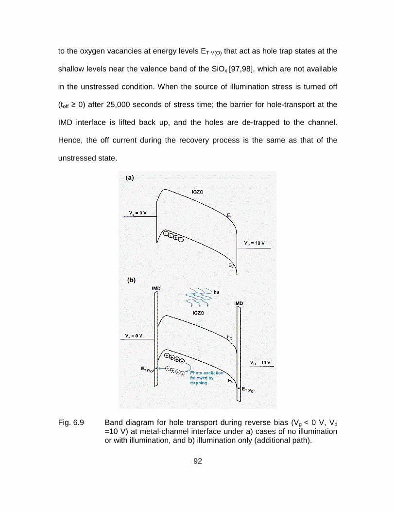
to the oxygen vacancies at energy levels E
shallow levels near the valence band of the SiO
in the unstressed condition. When the source of illumination stress is turned
(toff ≥ 0) after 25,000 seconds of stress time; the barrier for hole
IMD interface is lifted back up, and the holes are de
Hence, the off current during the recovery process is the same as that of the
unstressed state.
Fig. 6.9 Band diagram for hole transport during reverse bias (V=10 V) at metalor with illumination, and b) illumination only (additional path).
92
to the oxygen vacancies at energy levels ET V(O) that act as hole trap states at the
shallow levels near the valence band of the SiOx [97,98], which are not available
in the unstressed condition. When the source of illumination stress is turned
0) after 25,000 seconds of stress time; the barrier for hole-transport at the
IMD interface is lifted back up, and the holes are de-trapped to the channel.
current during the recovery process is the same as that of the
Band diagram for hole transport during reverse bias (V=10 V) at metal-channel interface under a) cases of no illumination or with illumination, and b) illumination only (additional path).
that act as hole trap states at the
], which are not available
in the unstressed condition. When the source of illumination stress is turned off
transport at the
trapped to the channel.
current during the recovery process is the same as that of the
Band diagram for hole transport during reverse bias (Vg < 0 V, Vd channel interface under a) cases of no illumination
or with illumination, and b) illumination only (additional path).
93
The positive effect of reduction in off current is usually nullified by a drop
in mobility and on current [99]. But in our study, we have observed reduced off
current as well as an increased on current during illumination testing, along with
a sizeable negative Vt shift. The higher field effect mobility is as a result of
increased free charge with respect to charge induced by gate voltage. The rate at
which excess charges are generated is a maximum during the first few minutes,
and decreases until the point where there is no significant change in the I-V
characteristics. This is due to the fact that the trap states in the deposited
gate/intermetal/interlayer dielectrics, and the channel are limited.
Another explanation towards increased on currents and reduced threshold
voltages can be provided through the role of oxygen vacancies created during
illumination [99]. Since photons of energy greater than that of the red light
wavelength are required to produce a negative bias illumination stress effect, it is
reasonable to consider the influence of oxygen vacancies because generation of
singly or doubly ionized vacancies from neutral vacancies requires an energy of
2.2 eV [100-102]. In amorphous metal oxide based transistors, conduction is
based on oxygen vacancies that act as dopants [25, 103] releasing electrons to
conduction band, hence reducing the threshold to turn on the device.
Earlier work [94] showed that when the light source is turned off, excess
electron-hole pairs generated by photons recombine, or the excess carriers from
the conduction band fall back into the deep level states. However in our study,
94
the incomplete recovery suggests that although the recombination of electron-
hole pairs is instantaneous, the carriers excited from the traps in the dielectric
materials and the channel fall back into the trap states over time due to
dependence on the diffusion length.
Holes generated through photonic generation also participate in the
generation of ionized vacancies that contribute to photon induced negative
threshold shift, as seen from the reactions below [104],
IGZO hυ e h− ++ → + (1)
( )2 (O) (O)
’’ desorption of oxygen OR2h O V 2eV + − −+ → + ++ (2)
(O) (O) desorption of oxygen’h O V V e − −+ + + → + + (3)
When the illumination stress is lifted, apart from the incomplete trapping of
electrons in original trap states, the passivation layer limits the oxygen
concentration to reverse the reactions (2) or (3).
Figure 6.10 illustrates the contribution of high energy photons towards excess
carriers in the conduction band by means of:
a) Excitation of carriers trapped in the deep states of the energy gap,
b) Generation of electron hole pairs, which later saturate due to an
increasing recombination rate,
c) Formation of doubly ionized vacancies due to the delocalization of
electrons from a neutral oxygen vacancy, followed by desorption of
oxygen.
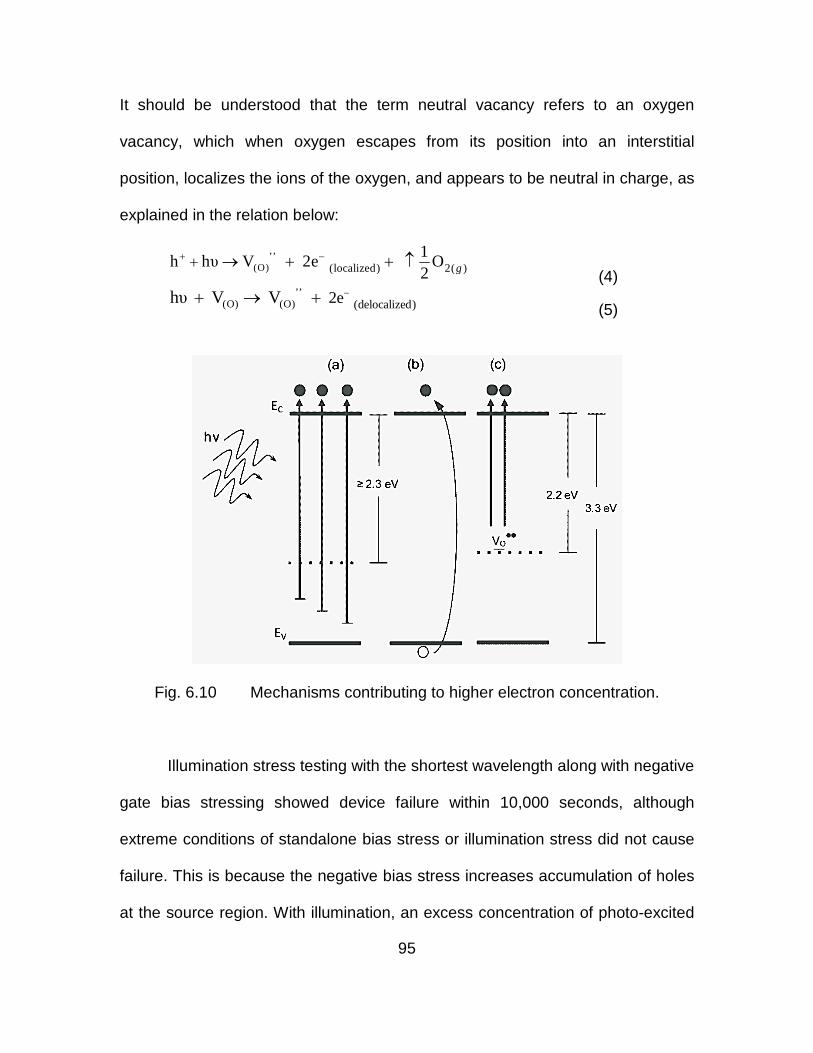
95
It should be understood that the term neutral vacancy refers to an oxygen
vacancy, which when oxygen escapes from its position into an interstitial
position, localizes the ions of the oxygen, and appears to be neutral in charge, as
explained in the relation below:
’’ (O) (localized) 2( )
1h hυ V 2e O
2 g+ −+ → + + ↑
(4) ’’
(O) (O) (delocalized) 2ehυ V V −+ → + (5)
Fig. 6.10 Mechanisms contributing to higher electron concentration.
Illumination stress testing with the shortest wavelength along with negative
gate bias stressing showed device failure within 10,000 seconds, although
extreme conditions of standalone bias stress or illumination stress did not cause
failure. This is because the negative bias stress increases accumulation of holes
at the source region. With illumination, an excess concentration of photo-excited
96
holes is trapped in the dielectric layers as discussed earlier and provides a
prominent early turn-on. When the channel is depleted of holes, the device fails
to function as a transistor and no more demonstrates an off-on behavior.
Conversely, although a positive gate voltage stress increased the threshold
voltage, when combined with illumination, it lead towards little to no threshold
shift indicating a compensational effect between the two phenomena.
Neither illumination nor bias stress testing have shown a considerable
increase in the subthreshold swing between the unstressed and the stressed
TFTs. Subthreshold swing is attributed to density of interface traps or defects
near the channel/insulator interface [105]. But the care taken in the fabrication
process by deposition of the dielectric at a high temperature (180 °C) and
performing a post-fabrication anneal, have reduced the density of defects to a
minimum. Deposition of an intermetal dielectric was effective in reducing the off
currents under stress conditions. Furthermore, although the power density of the
source of light used is greater than orders of 10’s of mW/cm2, the devices have
not failed (as could be seen with lower intensity illumination stressed TFTs
previously [94, 95]), probably due to a lesser number of oxygen vacancies
remaining after the fabrication, and also due to the protective encapsulation
layer. Apart from the gate and intermetal dielectrics delaying the recovery after
illumination stresses, the encapsulation layer could also be the reason behind the
incomplete recovery since the reactions illustrated above could be reversible if
there is oxygen readily available for adsorption. Adding oxygen creates neutral
97
vacancies once again, and results in recombination of the excessive electrons
with the holes obtained as a byproduct of the reaction.
6.5. Conclusion
The effect of the practical stress conditions such as illumination of visible
light, combined with prolonged electrical stress has been investigated. The
conditions that result in failure of TFTs within hours of operation were identified,
along with the responsible mechanisms. The large negative threshold voltage
shift encountered resulted from the ionizing of oxygen vacancies and contributed
excess electrons to the conduction band; whereas the large threshold voltage
shift under positive gate stress was the consequence of charge trapping
mechanism. The rate of charge trapping followed an exponential dependence on
time. The TFTs under stress demonstrated favorable trends such as, enhanced
mobilities, increased on currents, minimized creation of interface trap states
(causing minimum subthreshold swing changes), and reduced off currents (a
consequence of the trapping of holes at the thin IMD overlap at the
source/channel region). These trends accentuated the sensitivity of design,
fabrication and post fabrication steps (i.e., high temperature dielectric stack
deposition, encapsulation-layer incorporation and post fabrication anneals).
Combinations of stress techniques were shown to function as compensational
techniques; where, the negative impact of one stress was compensated for by
the impact of another stress. In this study, we were able to explain several effects
pertaining to wavelengths of light used, and positive and negative bias stress
98
applied for extended periods of time. Our findings however confirmed that further
research is needed to elucidate how the stress can be recovered/ unrecovered
and used to our advantage based on the device requirements for specific
applications.
99
Chapter 7
SUMMARY
7.1 Introduction
This chapter discusses the industry needs and concerns regarding
processes involved in treating ion implanted materials and thin film devices. The
post implantation processing techniques commonly used, such as laser anneal,
metal induced crystallization, and rapid thermal anneal have been explained in
brief. The disadvantages caused due to each of these methods are the
motivation behind the study of microwave anneal as an alternative process
technique. The microwave anneal has been found to be due to loss mechanisms,
and dielectric properties of the material. This knowledge gives us an
understanding of how anneal process would affect different materials differently,
and what considerations can be made while annealing materials with different
properties. For example, our study of arsenic implanted Si and previous research
of boron implanted Si shows that the samples were treated differently (one using
hybrid heating mechanism and the other by volumetric mechanism) due to
material dielectric properites, although the underlying process in both cases is
microwave anneal. Hence, in our study, a susceptor providing surface heating
was necessitated to allow the sample to absorb the microwave radiation and
undergo volumetric heating.
100
7.2 Materials Characterization
The As implanted Si, and as-implanted Si samples were annealed for
various time durations in the microwave cavity applicator by incorporating the
susceptor into the setup. A few runs of the experiment were repeated by
eliminating the use of the susceptor. To observe the material properties pre and
post anneal, several characterization techniques were used. The samples were
characterized to observe differences in structure, topology, and electrical
properties before and after anneal. Electrical characterization using four point
probe measurements and Hall measurements provided sheet resistance,
resistivity, mobility, and sheet concentration information. Ion channeling was
performed on the samples to ascertain the extent of damage repair possible by
microwave anneal mechanism. Cross-section transmission electron microscopy
(XTEM) patterns provided information on structural changes caused by
annealing. Raman spectroscopy also provided extent of damage repair or
recrystallization of the samples. Secondary ion mass spectrometry (SIMS) was
performed to verify if the anneal process caused any undesired dopant diffusion
into the substrate. Each of these characterization techniques were explained in
detail in chapter 2.
101
7.3 Dopant Activation and Dopant Diffusion of As implanted Si
The As implanted Si samples of different dosage and implantation energy
were annealed for different times with susceptor, and electrical characterization
techniques such as 4-point probe and Hall measurements were used to derive
data to verify dopant activation and dopant diffusion. Microwave anneal process
was successful in electrically activating the dopants, suggested by low sheet
resistances, and high sheet concentrations. Ion channeling data supports dopant
activation by the relocation of dopant atoms into substitutional sites instead of off-
lattice sites. SIMS was performed to analyze any possible dopant diffusion,
comparing the results against a 30 second annealed sample at 900 °C. The
results indicated minimal dopant diffusion using microwave anneal. The
microwave heating mechanism was discussed in detail supporting the use of a
susceptor to obtain quick recrystallization, and dopant activation, and minimum
dopant diffusion in As implanted Si.
102
7.4 Recrystallization of As implanted Si and as-implanted Si
Arsenic implanted, and silicon implanted Si samples, of the same extent of
damage were considered. The influence of material properites on anneal
mechanism was proved by annealing the 2 types of samples without susceptor.
The samples were annealed both with, and without susceptor for different
durations. Raman spectroscopy was performed, which provided data supporting
quick recrystallization providing a good quality single crystal Si by
recrystallization. Ion channeling was also performed on as-implanted Si annealed
with and without susceptor, showing no damage repair of the lattice when a
susceptor was not used. XTEM images confirm the recrystallization of the entire
amorphized layer of the As implanted Si samples. The rate of recrystallization
obtained by microwave anneal were compared to the rate of recrystallization due
to solid phase epitaxy, and the microwave anneal was found to produce a higher
rate of regrowth.
103
7.5 Kinetic stress testing and influence of long time anneals on the
behavior of IZO TFTs
A long time anneal in air ambient at 150 °C (which is compatible with
electronics on polymer substrates, and devices containing encapsulation layers)
has proved to improve the stability of devices under extended periods of bias and
thermal stress. The 12 hr and 48 hr annealed samples demonstrated the best
stability under bias stress, by undergoing minimum mobility and threshold voltage
shifts, however the 12 hr anneal was insufficient to cure the donor and acceptor
like defect states. The 48 hr anneal was effective in reducing the concentration of
traps to insignificant amounts. Furthermore, the study successfully describes the
thermionic emission and thermionic field emission mechanisms leading to device
failure, as well as elucidates the kink and dip phenomena to help elucidate better
post-processing steps.
104
7.6 Investigation of Defect Generation and Annihilation in IGZO TFTs
during Practical Stress Conditions: Illumination and Electrical Bias
The phenomena guiding mixed-oxide based transistors into failure while
under practical stress scenarios for a prolonged duration of time were
investigated. However, the degradation due to intrinsic defect centers were
reduced by a large extent due to the appropriate post anneal steps. TFTs with
lower off currents under negative bias illumination stress were achieved. The
post fabrication anneal was also efficient in regulating the density of oxygen
vacancies which could have been suppliers of excessive electrons, and reduced
the density of traps at the semiconductor/dielectric interface which has an effect
on the subthreshold swing of the device, crucial for fast switching speeds of
devices. The Ion/Ioff ratio in most stressed TFTs increased instead of
decreasing.
This can result in faster performance of active electronics based on TFTs
even under extreme practical stress conditions. With more investigation and
deeper understanding of the oxygen vacancies acting as dopants by ionizing,
fabrication and post fabrication suggestions can be made to reduce the density of
excess carriers being generated into the conduction band, so that failure of the
devices can be averted under illumination of any visible wavelength light.
105
7.7 Conclusion
The importance of novel anneal methods has been established in this
research, firstly in terms of a rapid microwave anneal method, and secondly by
low temperature designed anneals in different ambients. This work supports the
microwave anneal technique as an alternate post implantation process
technique. The innovative use of a susceptor to provide additional heating to a
high Z material like As, not only brought about faster recrystallization and dopant
activation, but also provids desirable results in terms of dopant diffusion by
indicating minimum diffusion of As into the Si. The susceptor’s surface heating
also enabled the formation of a good quality single crystal doped Si, instead of
formation of poly-Si which is possible due to insufficient heating. The successful
recrystallization of the high energy implanted samples suggests that irrespective
of the damage, the susceptor assisted anneal can provide heating sufficient to
overcome the high activation energy required to form single crystal Si, and
facilitate quick recrystallization of a thick damaged layer.
Low temperature deposited mixed oxide based thin film transistors which
are high in defect density due to the fabrication process, were annealed in
oxygen, forming gas and vacuum ambients at low temperatures. The anneals
proved to enhance the reliability of the TFTs under extreme stress conditions
such as illumination, bias and thermal stresses. The designed ambients gave in
depth knowledge of the nature of donors and defects within the mixed oxide
106
films, and lead way to study on the role of hydrogen as a donor within the mixed
oxide films. This was confirmed by elastic recoil detection (ERD) by corroborating
the density of hydrogen in the mixed oxide films to the conductivity and carrier
concentration (obtained from Hall measurements).
107
7.8 Future Work
In order to incorporate the microwave anneal technology into the current
industry requirements operating at a less than 17 nm node, further research can
be performed on low energy implanted samples. Also, focus can be laid on
achieving zero dopant diffusion. Efforts should be put into achieving thin film
transistors with low defect density. Deep level transient spectroscopy (DLTS) will
be used to identify the deep level defects within the mixed oxide thin films used
as channel materials, and an understanding of the interface states can also be
obtained for low temperature deposited dielectric and semiconductor materials.
These properties are crucial for improving performance and life time of low
temperature deposited thin film devices. Microwave anneal technology can be
extended as an anneal method for thin film transistors while maintaining
compatibility with flexible polymer substrates which facilitates large area
fabrication.
108
REFERENCES
[1] Y. Lee, F. Hsueh, S.Huang, J. Kowalski, A. Cheng, A. Koo, G.L.Luo, and C.Y.Wu, “A low-temperature microwave anneal process for boron-doped ultrathin Geepilayer on Si substrate”, IEEE Electron Dev. Lett., vol. 30, no. 2, pp. 123-125, 2009.
[2] K. M. Klein, C. Park, and A. F. Tasch, Appl. Phys. Lett., 57, 25 (1990) [3] K. M. Klein, C. Park, and A. F. Tasch, Nuc. Instr. And Meth. in Phys. Res.,
B59/60, 60 (1991) [4] C. Tian, S.Gara, G. Hobler, and G. Stingeder, Microchimica Acta, 107,
161 (1992) [5] G. Pepponi, D. Giubertoni, S. Gennaro, M. Bersani, M. Anderle, R.
Grisenti, M. Werner, and J. A. van den Berg, in Ion Implantation Technology, Marseille, France, edited by K. J. Kirkby, R. Gwilliam, A. Smith, and D. Chivers (AIP, New York, 2006),117 (2006)
[6] J.Ahn, J. Lee, Y.Kim, and B.Ahn, Current Applied Physics, 2, 135, (2002). [7] Y. Lee, F. Hsueh, S.Huang, J. Kowalski, A. Cheng, A. Koo, G. Luo, and C.
Wu, IEEE Electron Device Letters, 30 (2), 123 (2009). [8] J. W. Mayer and S. S. Lau, Electronic Materials Science: For Integrated
Circuits in Si and GaAs, Macmillan, New York, (1990) [9] T.Matsuyama, N.Terada, T. Baba, T. Sawada, S. Tsuge, K. Wakisaka,
and S.Tsuda, J Non-Cryst Solids, 940, 198 (1996). [10] R.B. Bergmann, G. Oswald, M. Albrecht, Gross V. SolEnergy Mater Sol
Cells, 46, 147 (1997). [11] K. Ishikawa, M. Ozawa, C. Oh , and M. Matsumura, Jpn J. Appl. Phys. 37,
731 (1998). [12] R. Kakkad, J. Smith, W.S. Lau, S.J. Fonash, and R. Kerns, J. Appl. Phys.
65, 206 (1989). [13] G. Huang, Z. Xi, and D. Yang, Vacuum 80, 415 (2006). [14] L. Hultman, A. Robertsson , H.T.G Hentzell, I. Engstrom, and PA. Psaras,
J Appl Phys, 62, 3647 (1987).
109
[15] Y.Woo, K.Kang, M.Jo, J.Jeon, and Miyoung Kim, Appl Phys Lett, 91, 223107 (2007).
[16] S. C. Fong, C. Y. Wang, T. H. Chang, and T. S. Chin, Appl Phys Lett, 94,
102104 (2009) [17] R. E. Newnham, S. J. Jang, M. Xu, and F. Jones. Fundamental Interaction
Mechanisms Between Microwaves and Matter. Ceramic Transactions, Microwaves: Theory and Application in Materials Processing, 21 (1991)
[18] C.Kittel, Solid State Physics, 2nd ed., New York: John Wiley and Sons
(1959) [19] P.Debye, Polar Molecules, Chemical Catalog Co., New York (1929) [20] D. C. Thompson, J. Decker, T. L. Alford, J. W. Mayer, and N. D.
Theodore, Mater. Res. Soc. Symp. Proc, 989, A06-18 (2007)
[21] Y. Sun and J. A. Rogers, Adv. Mater. 19, 1897 (2007). [22] J. Song, J. –S. Park, H. Kim, Y. – W. Heo, J. –H. Lee, J. –J. Kim, G. M.
Kim, and B. D. Choi, Appl. Phys. Lett. 90, 022106 (2007). [23] K. Nomura, H. Ohta, A. Takagi, T. Kamiya, M. Hirano and H. Hosono,
Nature 432, 288 (2004). [24] E. Fortunato, P. Barquinha, A. Pimentel, A. Gonçalves, A. Marques, R.
Martins and L. Pereira, Appl. Phys. Lett. 85, 2541 (2004). [25] N. L. Dehuff, E. S. Kettenring, D. Hong, H. Q. Chiang, J. F. Wager, R. L.
Hoffman, C.-H. Park and D. A. Keszler, J. Appl. Phys. 97, 064505 (2005). [26] E. Fortunato, P.M.C. Barquinha, A.C.M.B.G. Pimentel, A.M.F. Gonçalves,
A.J.S. Marques, L.M.N. Pereira and R. Martins, Adv. Mater. 17, 590 (2005).
[27] Y. S. Jung, J. Y. Seo, D. W. Lee, and D. Y. Jeon, Thin Solid Films 445, 63
(2003). [28] P. F. Carcia, R. S. McLean, and M. H. Reilly, and G. Nunes, Appl. Phys.
Lett. 82, 1117 (2003). [29] E. Fortunato, A. Pimentel, L. Pereira ,A. Gonçalves, G. Lavareda, H.
Aguas, I. Ferreira, C. N. Carvalho, and R. Martins, J. Non-Cryst. Solids 806, 338 (2004).
110
[30] R. E. Presley, C. L. Munsee, C. –H. Park, D. Hong, J. F. Wager, and D. A.
Keszler, J. Phys. D. 37, 2810 (2004). [31] Dhananjay, C. W. Chu, Appl. Phys. Lett. 91, 132111 (2007). [32] H. Yabuta, M. Sano, K. Abe, T. Aiba, T. Den, H. Kumomi, K. Nomura, T.
Kamiya, and H. Hosono, Appl. Phys. Lett. 89, 112123 (2006) [33] T. Minami, J. Vac. Sci. Technol. A 17, 1765 (1999) [34] T. Sasabayashi, N. Ito, E. Nishimura, M. Kon, P. K. Song, K. Utsumi, A.
Kaijo, and Y. Shigesato, Thin Solid Films 445, 219 [35] C.D.Poweleit, A.Gunther, S.Goodnick, and J. Mene´ndez, Appl Phys Lett,
73, 16 (1998) [36] W. K. Chu, J. W. Mayer, and M. A. Nicolet, Backscattering Spectroscopy
(Academic press, San Diego, CA), 4, (1978). [37] L. A. Giannuzzi, F. A. Stevie, Introduction to Focused Ion Beams, (2005). [38 R. Rao and G.C. Sun, Journal of Crystal Growth, 273, 68 (2004) [39] T. L. Alford, D. C. Thompson, J. W. Mayer, and N. D. Theodore, J. Appl.
Phys. 106, 114902 (2009) [40] T. L. Alford, L. C. Feldman, and J. W. Mayer, Fundamentals of Nanoscale
Film Analysis (Springer, New York, 2008) [41] A. C. Metaxas and R. J. Meredith, Industrial Microwave Heating, IEEE
Power Engineering Series 4 (Peter Peregrinus, London, 1983) [42] W.H. Sutton, Am. Ceram. Soc. Bull. 68 (2), 376 (1989) [43] D. E. Clark, D. C. Folz, J. K. West, Mat. Science and Engineering A287,
153 (2000) [44] D. R. Gaskell, Introduction to the Thermodynamics of Materials, Taylor &
Francis, Levittown, PA, (1995) [45] M. M. Bulbul, Microelectronic Engineering, 84, 124 (2007) [46] A. I. Shkrebtii, Z. A. Ibrahim, T. Teatro, W. Richter, M.J.G. Lee, and L.
Henderson, Phys. Status Solidi B 247(8), 1881 (2010)
111
[47] W.Bohmayr, A.Burenkov, J.Lorenz, H.Ryssel, S.Selberherr, IEEE
Transactions on Computer-Aided Design of Integrated Circuits and Systems, 17 (12), 1236 (1998)
[48] G.M.Crean, P.D.Cole, C.Jeynes, Solid State Electronics, 33 (6), 655
(1990) [49] E. Kinsbron, M.Sternheim, and R.Knoell, Appl. Phys. Lett., 42, 835 (1983) [50] M. A. Janney, H. D. Kimrey, M. A. Schmiat, and J. O. Kiggan, J. Am.
Ceram. Soc. 74, 1675 (1991) [51] J. N. Lee, Y.W. Choi, B. J. Lee, and B.T. Ahn, J. Appl. Phys. 82, 6 (1997) [52] S. N. Hsu and L. J. Chen, Appl. Phys. Lett., 55 (22), 2305 (1989) [53] J. W. Christian, The Theory of Transformations in Metals and Alloys, Part
1, 3rd ed. Elsevier Science, Oxford, Version 1, Chap. 11, 482 (2002) [54] S.M. Zanetti, J.S. Vasconcelos, N.S.L.S. Vasconcelos, E.R. Leite, E.
Longo, and J.A. Varela, Thin Solid Films, 466, 62 (2004) [55] J. W. Mayer, S. S. Lau, Electronic Materials Science: For Integrated
Circuits in Si and GaAs, Macmillan Publishing Company, New York, NY (1990)
[56] J. D. Plummer, M. D. Deal, P. B. Griffin, Silicon VLSI Technology:
Fundamentals, Practice and Modeling, Prentice Hall, Upper Saddle River, NJ (2000).
[57] R. B. M. Cross and M. M. De Souza, Appl. Phys. Lett., 89, 263513 (2006)
[58] I.-T. Cho, J.-M. Lee, J.-H. Lee, and H. -I. Kwon, Semicond. Sci. Technol.,
24, 015013 (2009) [59] T.-C. Fung, K. Abe, H. Kumomi, and J. Kanicki, Jour. Disp. Technol.,
5(12), 452 (2009) [60] K. Kaftanoglu, S. M. Venugopal, M. Marrs, A. Dey, E. J. Bawolek, D. R.
Allee, and D. Loy, Jour. Disp. Technol., 7(6), 339 ( 2011) [61] E. N. Cho, J. H. Kang, C. E. Kim, P. Moon, and I. Yun ,IEEE Trans.
Device Mater. Reliab., 11(1), 112 (2011)
112
[62] K. Hoshino, and J. F. Wager, IEEE Elec. Dev. Lett., 31(8), 818 (2010) [63] J.-S. Jung, K.-S. Son, T.-S. Kim, M.-K. Ryu, K.-B. Park, B.-W. Yoo, J.-Y.
Kwon, S.-Y. Lee, and J.-M. Kim, ECS Trans.,16(9), 309 (2008) [64] A. Indluru, S. M. Venugopal, D. R. Allee, and T. L. Alford, Mater. Res. Soc.
Symp. Proc., paper no.1245-A19-02 (2010) [65] C.-H. Li, Y.-S. Tsai, and J. Z. Chen, Semiconductor Science and
Technology, 26 (10), 105007 (2011) [66] A. Indluru, and T. L. Alford, Electrochem. and Solid-State Lett., 13(12),
H464 (2010) [67] D. Zhou, M. Wang, H. Li, and J. Zhou, 2010 17th IEEE International
Symposium on the Physical and Failure Analysis of Integrated Circuits (IPFA), 1 (2010)
[68] M. Furuta, Y. Kamada, M. Kimura, T. Hiramatsu, T. Matsuda, H. Furuta,
C. Li, S. Fujita, and T. Hirao, IEEE Elec. Dev. Lett., 31 (11), 1257 (2010) [69] M. H. Chang, J. F. Zhang, Semiconductor Science and Technology, 19,
1333 (2004) [70] Y. Kuo, “Thin film transistors materials and processes Vol 1: Amorphous
silicon thin film transistors”, Kluwer Academic, Boston, 2004. [71] J. Tan, A. Baiano, R. Ishihara, and K. Beenakker, CIM (2008), The annual
workshop on semiconductor advances for future electronics and sensors, Veldhoven, The Netherlands: STW., 600 (2008)
[72] Y.-S. Tsai and J.-Z. Chen, IEEE Trans. Elec. Dev., 59(1), 151 (2012) [73] H. Schulz and K. H. Theimann, “ Structure parameters and polarity of the
wurtzite type compounds SiC-2H and ZnO”, Solid State Commun., 32(9), 783 (1979)
[74] M. Koyanagi, Y. Baba, K. Hata, I. –W. Wu, A. G. Lewis, M. Fuse, and R.
Bruce, IEEE Elec. Dev. Lett., 13(3), 152 (1992) [75] K.-J. Kim, W.-K. Park, S.-G. Kim, K.-M. Lim, I.-G. Lim, and O. Kim, Solid
State Elec., 42(11), 1897 (1998) [76] H. Tsuji, Y. Kamakura, and K. Taniguchi, ECS Trans., 33(5), 105 (2010)
113
[77] M. Bae, Y. Kim, S. Kim, D. M. Kim, and D. H. Kim, IEEE Elec. Dev. Lett., 32(9), 1248 (2011)
[78] H.-H. Hsieh, T. Kamiya, K. Nomura, H. Hosono, and C.-C. Wu, Appl. Phy.
Lett., 92, 133503 (2008) [79] F. M. Hossain, J. Nishii, S. Takagi, A. Ohtomo, T. Fukumura, H. Fujioka,
H. Ohno, H. Koinuma, and M. Kawasaki, Jour. Appl. Phy., 94(12), 7768 (2003)
[80] G. Baccarani, B. Ricco, and G. Spadini, Jour. Appl. Phy., 49 (11), 5565
(1978) [81] J. Levinson, F. R. Shepherd, P. J. Scanlon, W. D. Westwood, G. Este, and
M. Rider, Jour. Appl. Phy., 53(2), 1193 (1982) [82] J. Puigdollers, C. Voz, A. Orpella, I. Martin, D. Soler, M. Fonrodona, J.
Bertomeu, J. Andreu, and R. Alcubilla, Jour. Non-Crystalline Solids, 299, 400 (2002)
[83] A.J. Leenheer, J.D. Perkins, M.F.A.M. Hest, and J.J. Berry, Phy. Rev. B
77, 115215 (2008) [84] M.K. Ryu, S. Yang, S –H K Park, C -S Hwang, and J K Jeong, Appl. Phys.
Lett. 95, 173508 (2009) [85] K. Sakariya, C.K.M. Ng, P. Servati, and A. Nathan A 2005 IEEE Trans. on
Elec. Dev. 52 (12), 2577 (2005) [86] K Kaftanoglu, S.M. Venugopal, M. Marrs, A. Dey, E.J. Bawolek, D.R.
Allee, and D. Loy, Jour. of Display Tech. 7 (6), 339 (2011) [87] H -C Cheng, C –F Chen, and C –C Lee, Thin Solid Films 498, 142 (2006) [88] R E Presley, C L Munsee, C -H Park, D Hong, J F Wager and D A
Keszler, J. Phys. D: Appl. Phys. 37, 2810 (2004) [89] N L Dehuff, E S Kettenring, D Hong, H Q Chiang, J F Wager, R L
Hoffman, C -H Park and D A Keszler, J. Appl. Phys. 97, 064505 (2005) [90] P. Görrn, P. Hölzer, T. Riedl, W. Kowalsky, J. Wang, T. Weimann, P.
Hinze, and S. Kipp, Appl. Phys. Lett. 90, 063502 (2007) [91] M.E. Lopes, H.L. Gomes, M.C.R. Medeiros, P. Barquinha, L. Pereira, E.
Fortunato, R. Martins, and I. Ferreira, Appl. Phys. Lett. 95, 063502 (2009)
114
[92] H. Kumomi, K. Nomura, T. Kamiya, and H. Hosono Thin Solid Films 516,
1516 (2008) [93] Y. Li, C.-H. Hwang, C.-L. Chen, S. Yan, and J –C Lou, IEEE Trans. on
Elec. Dev. 55, 11 (2008) [94] K.W. Lee, K M Kim, K Y Heo, S K Park, S K Lee, H J Kim, Current Appl.
Phys. 11, 280 (2011) [95] A. Indluru and T.L. Alford, Electrochem. Solid-State Lett. 13 (12), 464
(2010) [96] D.C. Paine, B. Yaglioglu, Z. Beiley and S. Lee Thin Solid Films 516, 5894
(2008) [97] J.H Kim, U.K. Kim, Y.J. Chung, and C.S. Hwang, Appl. Phys. Lett. 98,
232102 (2011) [98] J -M Kim, S J Lim, T Nam, D Kim, and H Kima Jour. of Electrochem. Soc.
158 (5), 150 (2011) [99] K W Lee, K Y Heo, and H J Kim, Appl. Phys. Lett. 94, 102112 (2009) [100] B. Ryu, H -K Noh, E -A Choi, and K J Chang, Appl. Phys. Lett. 97, 022108
(2010) [101] J. Robertson, Rep. Prog. Phys. 69 327 (2006) [102] K H Ji, J -I Kim, H Y Jung, S Y Park, R Choi, U K Kim, C S Hwang, D Lee,
H Hwang, and J K Jeong, Appl. Phys. Lett. 98, 103509 (2011) [103] K -H Lee, J S Jung, K S Son, J S Park, T S Kim, R Choi, J K Jeong, J -Y
Kwon, B Koo, and S Lee, Appl. Phys. Lett. 95, 232106 (2009) [104] B Ryu, H -K Noh, E -A Choi, and K J Chang, Appl. Phys. Lett. 97, 022108
(2010) [105] A Janotti and C G Van de Walle, Phys. Rev. B 76 165202 (2007) [106] M D H Chowdhury, P Migliorato, and J. Jang, Appl. Phys. Lett. 97 173506 [107] N L Dehuff, E S Kettenring, D Hong, H Q Chiang, J F Wager, R L
Hoffman, C H Park, and D A Keszler, J. Appl. Phys. 97, 064505 (2005)
115
[108] B Yaglioglu, H Y Yeom, R Beresford, and D C Paine, Appl. Phys. Lett. 89 062103 (2006)
[109] M. J. Gadre and T. L. Alford, Appl. Phys. Lett. 99, 051901 (2011) [110] A Rolland, J Richard, J P Kleider, and D Mencaraglia, J. Electrochem.
Soc. 140, 3679 (1993)