Embed Size (px)
Citation preview
arX
iv:q
uant
-ph/
0302
166v
1 2
1 F
eb 2
003
1
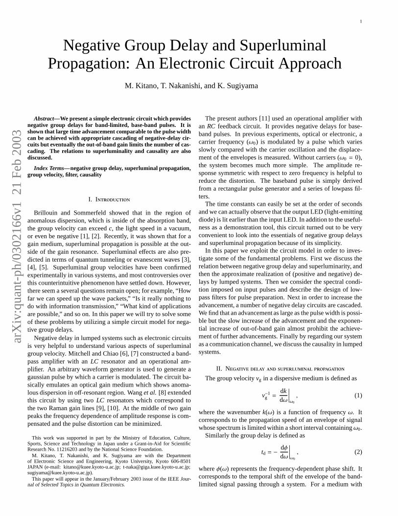
Negative Group Delay and SuperluminalPropagation: An Electronic Circuit Approach
M. Kitano, T. Nakanishi, and K. Sugiyama
Abstract—We present a simple electronic circuit which providesnegative group delays for band-limited, base-band pulses.It isshown that large time advancement comparable to the pulse widthcan be achieved with appropriate cascading of negative-delay cir-cuits but eventually the out-of-band gain limits the numberof cas-cading. The relations to superluminality and causality arealsodiscussed.
Index Terms—negative group delay, superluminal propagation,group velocity, filter, causality
I. I
Brillouin and Sommerfeld showed that in the region ofanomalous dispersion, which is inside of the absorption band,the group velocity can exceedc, the light speed in a vacuum,or even be negative [1], [2]. Recently, it was shown that for again medium, superluminal propagation is possible at the out-side of the gain resonance. Superluminal effects are also pre-dicted in terms of quantum tunneling or evanescent waves [3],[4], [5]. Superluminal group velocities have been confirmedexperimentally in various systems, and most controversiesoverthis counterintuitive phenomenon have settled down. However,there seem a several questions remain open; for example, “Howfar we can speed up the wave packets,” “Is it really nothing todo with information transmission,” “What kind of applicationsare possible,” and so on. In this paper we will try to solve someof these problems by utilizing a simple circuit model for nega-tive group delays.
Negative delay in lumped systems such as electronic circuitsis very helpful to understand various aspects of superluminalgroup velocity. Mitchell and Chiao [6], [7] constructed a band-pass amplifier with anLC resonator and an operational am-plifier. An arbitrary waveform generator is used to generateagaussian pulse by which a carrier is modulated. The circuit ba-sically emulates an optical gain medium which shows anoma-lous dispersion in off-resonant region. Wanget al. [8] extendedthis circuit by using twoLC resonators which correspond tothe two Raman gain lines [9], [10]. At the middle of two gainpeaks the frequency dependence of amplitude response is com-pensated and the pulse distortion can be minimized.
This work was supported in part by the Ministry of Education,Culture,Sports, Science and Technology in Japan under a Grant-in-Aid for ScientificResearch No. 11216203 and by the National Science Foundation.
M. Kitano, T. Nakanishi, and K. Sugiyama are with the Departmentof Electronic Science and Engineering, Kyoto University, Kyoto 606-8501JAPAN (e-mail: [email protected]; [email protected];[email protected]).
This paper will appear in the January/February 2003 issue of the IEEEJour-nal of Selected Topics in Quantum Electronics.
The present authors [11] used an operational amplifier withan RC feedback circuit. It provides negative delays for base-band pulses. In previous experiments, optical or electronic, acarrier frequency (ω0) is modulated by a pulse which variesslowly compared with the carrier oscillation and the displace-ment of the envelopes is measured. Without carriers (ω0 = 0),the system becomes much more simple. The amplitude re-sponse symmetric with respect to zero frequency is helpful toreduce the distortion. The baseband pulse is simply derivedfrom a rectangular pulse generator and a series of lowpass fil-ters.
The time constants can easily be set at the order of secondsand we can actually observe that the output LED (light-emittingdiode) is lit earlier than the input LED. In addition to the useful-ness as a demonstration tool, this circuit turned out to be veryconvenient to look into the essentials of negative group delaysand superluminal propagation because of its simplicity.
In this paper we exploit the circuit model in order to inves-tigate some of the fundamental problems. First we discuss therelation between negative group delay and superluminarity, andthen the approximate realization of (positive and negative) de-lays by lumped systems. Then we consider the spectral condi-tion imposed on input pulses and describe the design of low-pass filters for pulse preparation. Next in order to increasetheadvancement, a number of negative delay circuits are cascaded.We find that an advancement as large as the pulse width is possi-ble but the slow increase of the advancement and the exponen-tial increase of out-of-band gain almost prohibit the achieve-ment of further advancements. Finally by regarding our systemas a communication channel, we discuss the causality in lumpedsystems.
II. N
The group velocityvg in a dispersive medium is defined as
v−1g =
dkdω
∣
∣
∣
∣
∣
ω0
, (1)
where the wavenumberk(ω) is a function of frequencyω. Itcorresponds to the propagation speed of an envelope of signalwhose spectrum is limited within a short interval containingω0.
Similarly the group delay is defined as
td = −dφdω
∣
∣
∣
∣
∣
ω0
, (2)
whereφ(ω) represents the frequency-dependent phase shift. Itcorresponds to the temporal shift of the envelope of the band-limited signal passing through a system. For a medium with
2
C
R
(a) (b)
C R
CR
R1 R1
(c)
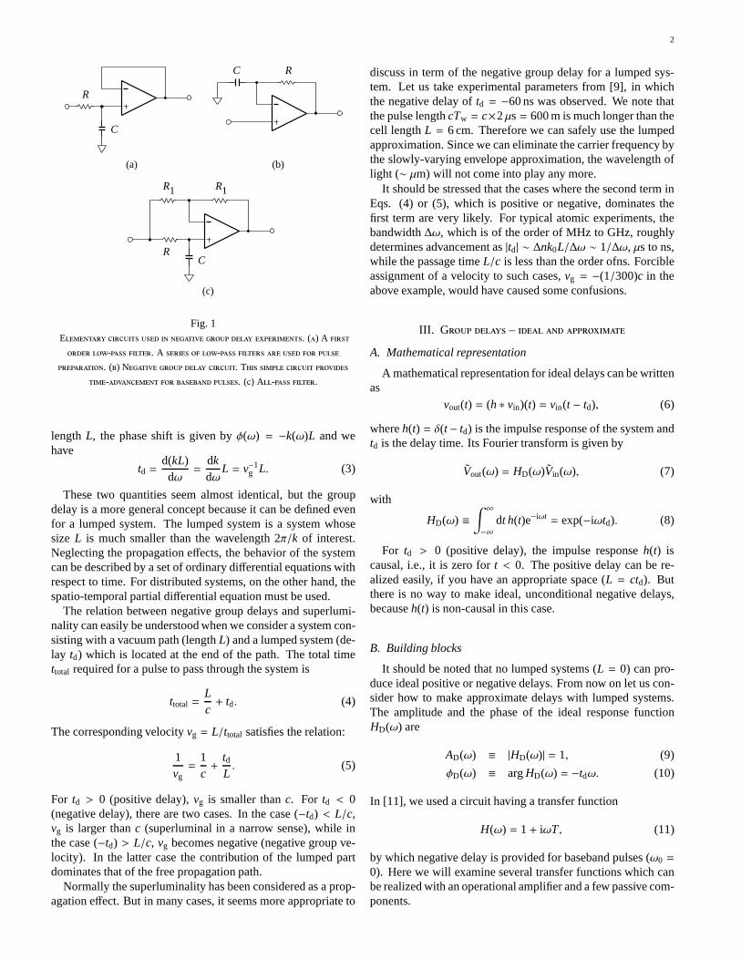
Fig. 1E . () A
- . A -
. () N . T
- . () A- .
length L, the phase shift is given byφ(ω) = −k(ω)L and wehave
td =d(kL)dω
=dkdω
L = v−1g L. (3)
These two quantities seem almost identical, but the groupdelay is a more general concept because it can be defined evenfor a lumped system. The lumped system is a system whosesize L is much smaller than the wavelength 2π/k of interest.Neglecting the propagation effects, the behavior of the systemcan be described by a set of ordinary differential equations withrespect to time. For distributed systems, on the other hand,thespatio-temporal partial differential equation must be used.
The relation between negative group delays and superlumi-nality can easily be understood when we consider a system con-sisting with a vacuum path (lengthL) and a lumped system (de-lay td) which is located at the end of the path. The total timettotal required for a pulse to pass through the system is
ttotal =Lc+ td. (4)
The corresponding velocityvg = L/ttotal satisfies the relation:
1vg=
1c+
tdL. (5)
For td > 0 (positive delay),vg is smaller thanc. For td < 0(negative delay), there are two cases. In the case (−td) < L/c,vg is larger thanc (superluminal in a narrow sense), while inthe case (−td) > L/c, vg becomes negative (negative group ve-locity). In the latter case the contribution of the lumped partdominates that of the free propagation path.
Normally the superluminality has been considered as a prop-agation effect. But in many cases, it seems more appropriate to
discuss in term of the negative group delay for a lumped sys-tem. Let us take experimental parameters from [9], in whichthe negative delay oftd = −60 ns was observed. We note thatthe pulse lengthcTw = c×2µs= 600 m is much longer than thecell lengthL = 6 cm. Therefore we can safely use the lumpedapproximation. Since we can eliminate the carrier frequency bythe slowly-varying envelope approximation, the wavelength oflight (∼ µm) will not come into play any more.
It should be stressed that the cases where the second term inEqs. (4) or (5), which is positive or negative, dominates thefirst term are very likely. For typical atomic experiments, thebandwidth∆ω, which is of the order of MHz to GHz, roughlydetermines advancement as|td| ∼ ∆nk0L/∆ω ∼ 1/∆ω, µs to ns,while the passage timeL/c is less than the order ofns. Forcibleassignment of a velocity to such cases,vg = −(1/300)c in theabove example, would have caused some confusions.
III. G –
A. Mathematical representation
A mathematical representation for ideal delays can be writtenas
vout(t) = (h ∗ vin)(t) = vin(t − td), (6)
whereh(t) = δ(t − td) is the impulse response of the system andtd is the delay time. Its Fourier transform is given by
Vout(ω) = HD(ω)Vin(ω), (7)
with
HD(ω) ≡∫ ∞
−∞dt h(t)e−iωt = exp(−iωtd). (8)
For td > 0 (positive delay), the impulse responseh(t) iscausal, i.e., it is zero fort < 0. The positive delay can be re-alized easily, if you have an appropriate space (L = ctd). Butthere is no way to make ideal, unconditional negative delays,becauseh(t) is non-causal in this case.
B. Building blocks
It should be noted that no lumped systems (L = 0) can pro-duce ideal positive or negative delays. From now on let us con-sider how to make approximate delays with lumped systems.The amplitude and the phase of the ideal response functionHD(ω) are
AD(ω) ≡ |HD(ω)| = 1, (9)
φD(ω) ≡ argHD(ω) = −tdω. (10)
In [11], we used a circuit having a transfer function
H(ω) = 1+ iωT, (11)
by which negative delay is provided for baseband pulses (ω0 =
0). Here we will examine several transfer functions which canbe realized with an operational amplifier and a few passive com-ponents.
3
First, we consider a function with a single pole:
HL(ω) =1
1+ iωT, (12)
AL(ω) = 1/√
1+ (ωT)2 ∼ 1− (ωT)2
2, (13)
φL(ω) = − tan−1ωT ∼ −Tω. (14)
The stability condition that all the poles reside in the upper halfplane requiresT > 0, therefore, only positive delaystd = T > 0can be achieved with this type of transfer function. An exampleof circuit is shown in Fig. 1(a). Only in the region|ω| < 1/T,the amplitude response is flat and the phase response is linear.The circuit works only for band-limited signals.
Secondly, we will check a function with a single zero:
H(ω) = 1+ iωT, (15)
A(ω) =√
1+ (ωT)2 ∼ 1+(ωT)2
2, (16)
φ(ω) = tan−1ωT ∼ Tω. (17)
In this case, no sign restrictions are imposed onT, therefore,both positive and negative delays can be realized;td = −T. Acircuit for H(ω) (T > 0) is shown in Fig. 1(b). Perhaps this isthe most simple circuit which provides negative delay. Again itworks only in the region|ω| < 1/T. Even worse is the risingof gainA(ω) at the outside of the band. We can also constructa positive delay circuit utilizing the relation 2− H(ω) = 1 +iω(−T).
By observing the sign restrictions forHL(ω) andH(ω), wenotice that an asymmetry between the positive and negative de-lays exists even in lumped systems.
Another interesting transfer function is
HA(ω) =1− iωT1+ iωT
, (18)
AA(ω) = 1, (19)
φA(ω) = −2 tan−1ωT ∼ −2Tω, (20)
which can be realized by the circuit shown in Fig. 1(c). This cir-cuit is called the all-pass filter. The phase function is the sameas the above cases aside from the factor 2, but the amplituderesponse in independent of the frequency as in the case of idealdelay. The stability condition impliesT > 0, therefore, onlypositive delays are possible.
IV. B
A. Bandwidth of negative delay circuit
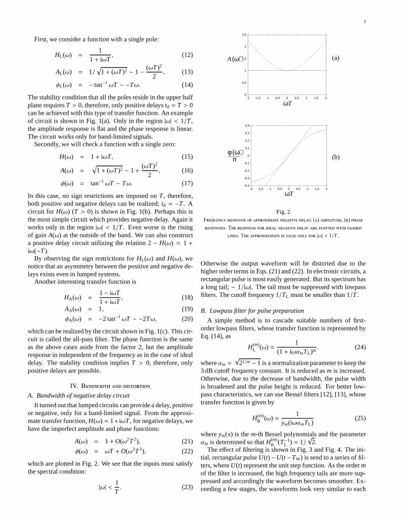
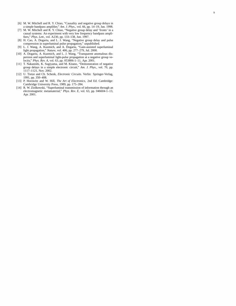
It turned out that lumped circuits can provide a delay, positiveor negative, only for a band-limited signal. From the approxi-mate transfer function,H(ω) = 1+ iωT, for negative delays, wehave the imperfect amplitude and phase functions:
A(ω) = 1+O(ω2T2), (21)
φ(ω) = ωT +O(ω3T3), (22)
which are plotted in Fig. 2. We see that the inputs must satisfythe spectral condition:
|ω| < 1T. (23)
(a)
(b)
A(ω)
φ (ω)
Tω
π
Tω
0
0.5
1
1.5
2
2.5
-2 -1.5 -1 -0.5 0 0.5 1 1.5 2
-0.4
-0.3
-0.2
-0.1
0
0.1
0.2
0.3
0.4
-2 -1.5 -1 -0.5 0 0.5 1 1.5 2
Fig. 2F ; () , ()
. T
. T |ω| < 1/T.
Otherwise the output waveform will be distorted due to thehigher order terms in Eqs. (21) and (22). In electronic circuits, arectangular pulse is most easily generated. But its spectrum hasa long tail;∼ 1/|ω|. The tail must be suppressed with lowpassfilters. The cutoff frequency 1/TL must be smaller than 1/T.
B. Lowpass filter for pulse preparation
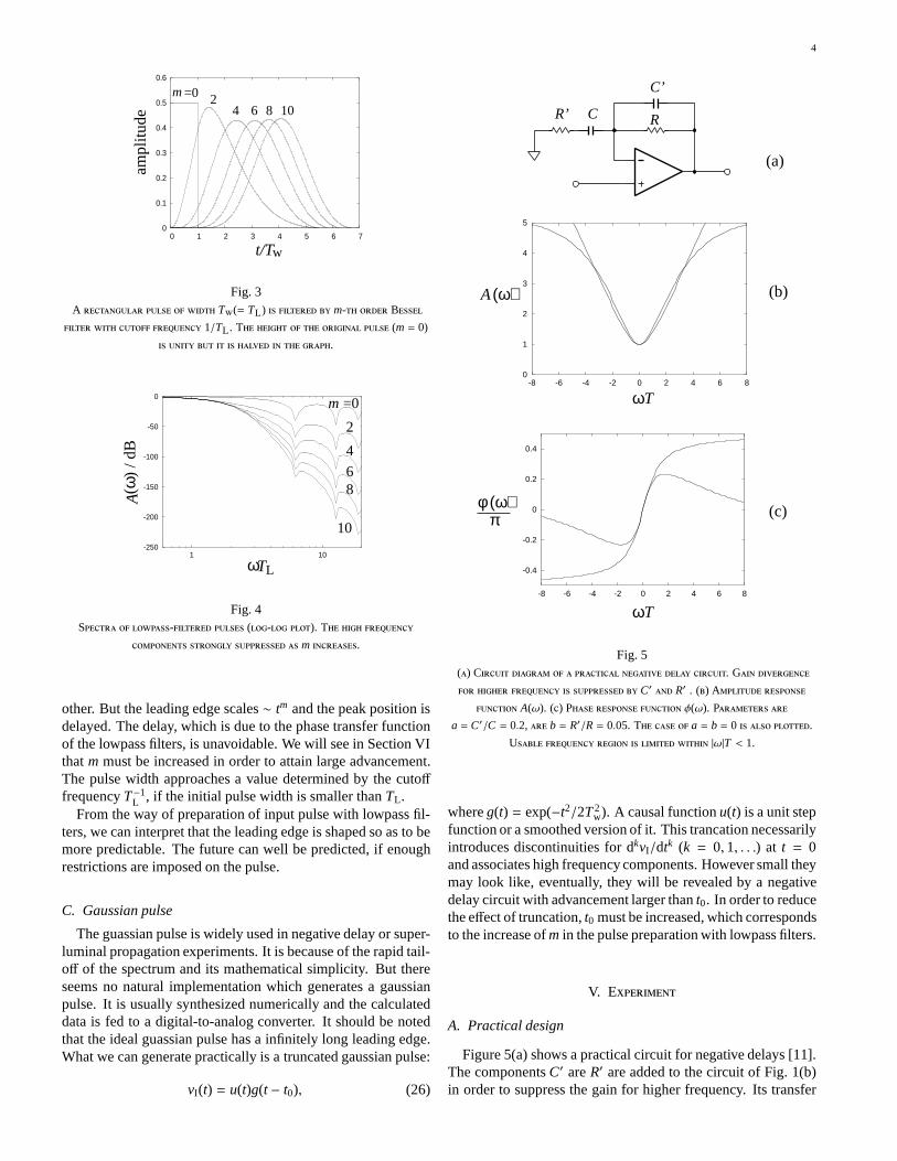
A simple method is to cascade suitable numbers of first-order lowpass filters, whose transfer function is represented byEq. (14), as
H(m)L (ω) =
1(1+ iωαmTL)m
. (24)
whereαm =√
21/m− 1 is a normalization parameter to keep the3 dB cutoff frequency constant. It is reduced asm is increased.Otherwise, due to the decrease of bandwidth, the pulse widthis broadened and the pulse height is reduced. For better low-pass characteristics, we can use Bessel filters [12], [13], whosetransfer function is given by
H(m)B (ω) =
1ym(iωαmTL)
(25)
whereym(x) is them-th Bessel polynomials and the parameterαm is determined so thatH(m)
B (T−1L ) = 1/
√2.
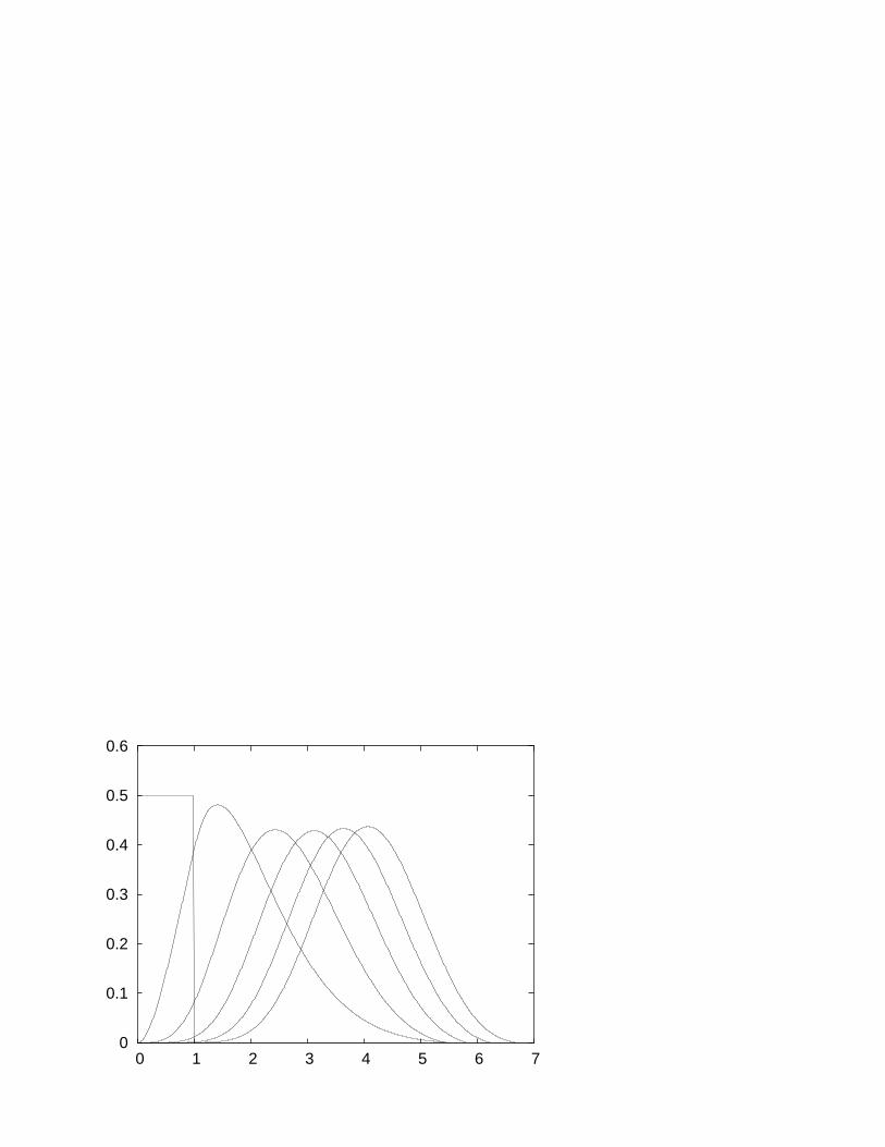
The effect of filtering is shown in Fig. 3 and Fig. 4. The ini-tial, rectangular pulseU(t)−U(t−TW) is send to a series of fil-ters, whereU(t) represent the unit step function. As the ordermof the filter is increased, the high frequency tails are more sup-pressed and accordingly the waveform becomes smoother. Ex-ceeding a few stages, the waveforms look very similar to each
4
0
0.1
0.2
0.3
0.4
0.5
0.6
0 1 2 3 4 5 6 7
24 6 8 10
m=0
t/Tw
ampl
itude
Fig. 3A T(= TL ) m- B
1/TL . T (m= 0)
.
-250
-200
-150
-100
-50
0
1 10
m =0
2
4
68
10
A(ω
) / d
B
ωTL
Fig. 4S - (- ). T
m .
other. But the leading edge scales∼ tm and the peak position isdelayed. The delay, which is due to the phase transfer functionof the lowpass filters, is unavoidable. We will see in SectionVIthatm must be increased in order to attain large advancement.The pulse width approaches a value determined by the cutoff
frequencyT−1L , if the initial pulse width is smaller thanTL.
From the way of preparation of input pulse with lowpass fil-ters, we can interpret that the leading edge is shaped so as tobemore predictable. The future can well be predicted, if enoughrestrictions are imposed on the pulse.
C. Gaussian pulse
The guassian pulse is widely used in negative delay or super-luminal propagation experiments. It is because of the rapidtail-off of the spectrum and its mathematical simplicity. But thereseems no natural implementation which generates a gaussianpulse. It is usually synthesized numerically and the calculateddata is fed to a digital-to-analog converter. It should be notedthat the ideal guassian pulse has a infinitely long leading edge.What we can generate practically is a truncated gaussian pulse:
vI(t) = u(t)g(t − t0), (26)
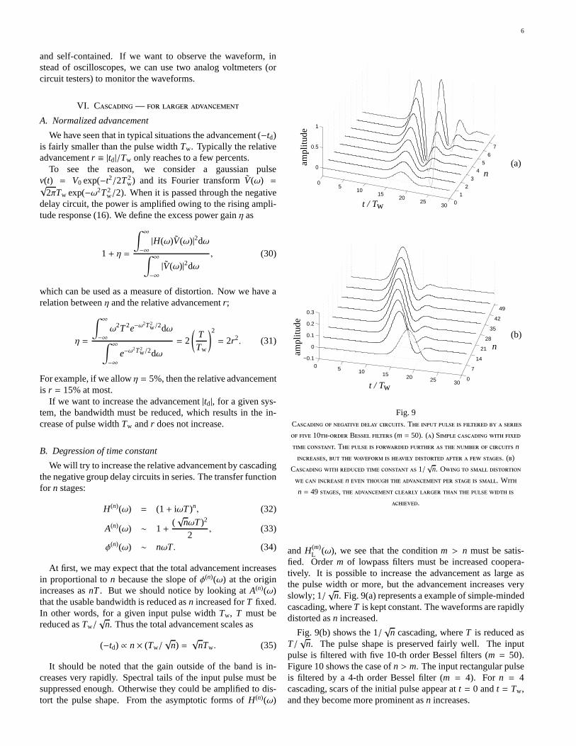
C R
C’
R’
(a)
(b)
(c)
A(ω)
φ (ω)
Tω
Tω
-0.4
-0.2
0
0.2
0.4
-8 -6 -4 -2 0 2 4 6 8
0
1
2
3
4
5
-8 -6 -4 -2 0 2 4 6 8
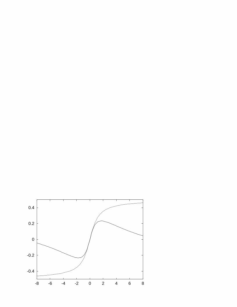
π
Fig. 5() C . G
C′ R′ . () A
A(ω). () P φ(ω). P
a = C′/C = 0.2, b = R′/R= 0.05. T a = b = 0 .
U |ω|T < 1.
whereg(t) = exp(−t2/2T2w). A causal functionu(t) is a unit step
function or a smoothed version of it. This trancation necessarilyintroduces discontinuities for dkvI/dtk (k = 0, 1, . . .) at t = 0and associates high frequency components. However small theymay look like, eventually, they will be revealed by a negativedelay circuit with advancement larger thant0. In order to reducethe effect of truncation,t0 must be increased, which correspondsto the increase ofm in the pulse preparation with lowpass filters.
V. E
A. Practical design
Figure 5(a) shows a practical circuit for negative delays [11].The componentsC′ areR′ are added to the circuit of Fig. 1(b)in order to suppress the gain for higher frequency. Its transfer

5
R1
R1 C1
C1
R2
R3
Fig. 62- B
Pulser Lowpass filtersSwitch
H ( )B
ω(2) H ( )B
ω(2)
Pulse generator
Negative delay circuit
NH ( )ω NH ( )ω
LEDin LEDout
Fig. 7E
function can easily be derived. First, we see that
V− =ZC
ZC + ZRVout, (27)
whereZC = R′ + 1/iωC, ZR = (R−1 + iωC′)−1. If we assume alarge gain of the operational amplifier, the virtual short condi-tion, Vin ∼ V−, holds and we have
HN(ω) = Vout/Vin
= (1+ ZR/ZC)
= 1+iωT
(1+ iωaT)(1+ iωbT), (28)
whereT = CR. If a ≡ C′/C ≪ 1 andb ≡ R′/R ≪ 1 aresatisfied, then the transfer function is approximated asHN(ω) ∼1 + iωT near the origin (|ω| < 1/T). Thanks toa or b, themaximum gain is limited by 1/(a+ b). The response functionsfor a = 0.2,b = 0.05 are plotted in Figs. 5(b) and (c). The phaseslope at the origin is almost conserved but the usable bandwidthis reduced.
Second-order Bessel filters are used in the experiment, be-cause the second-order filter can be realized with an operationalamplifier [12], [13]. The circuit diagram is shown in Fig. 6. The
-0.5
0
0.5
1
1.5
2
2.5
-1 0 1 2 3 4 5 6 7
time / s
ampl
itude
/ V inputoutput
Fig. 8E . T
. P 0.5 s.
frequency response is
H(2)B (ω) =
11+ iωα2TL + (iωα2TL)2/3
, (29)
whereTL = 1.272R1C1 is the inverse of cutoff frequency andR3/R2 = 0.268.
B. Experimental result
In Fig. 7, we show the overall block diagram for the neg-ative delay experiment. The complete circuit diagram is pre-sented in [11]. The pulse generator on the top is composed ofa single-shot pulser and two 2nd-order Bessel filters. Triggeredby the switch, a timer IC (ICM7555) generates a rectangularpulse with duration 1.5 s. The pulse is shaped by the filters.The cut-off frequency is chosen asωc = 1/TL = 0.35/T, sothatA(ω) andφ(ω) can be considered to be constant and linear,respectively.T = CR is the time constant of the negative delaycircuits.
Two negative delay circuits are cascaded for larger advance-ment. The circuit parameters areR = 1 MΩ, C = 0.22µF,a = 0.1, b = 0.01.
The input and output terminals are monitored by LEDs.Their turn-on voltage is about 1.1V.
The experimental result is shown in Fig. 8. The input andoutput waveforms are recorded with an oscilloscope. The timeorigin (t = 0) is the moment when the switch is turned on or therising edge of the initial rectangular pulse.
We see that the output pulse precedes the input pulse consid-erably (more than 20% of the pulse width). The slight distortionof the output waveform is caused by the non-ideal frequencydependence ofA(ω) andφ(ω).
The observed advancement of∼ 0.5 s agrees well with theexpected value 2T = 2CR= 0.44 s.
General purpose operational amplifiers (TL082) are used forlow-pass filters and negative delay circuits. The time scalehasbeen chosen so that we can directly observe the negative de-lay with two LEDs connected at the input and the output ter-minals. The whole experimental setup can be battery-operated
6
and self-contained. If we want to observe the waveform, instead of oscilloscopes, we can use two analog voltmeters (orcircuit testers) to monitor the waveforms.
VI. C—
A. Normalized advancement
We have seen that in typical situations the advancement (−td)is fairly smaller than the pulse widthTw. Typically the relativeadvancementr ≡ |td|/Tw only reaches to a few percents.
To see the reason, we consider a gaussian pulsev(t) = V0 exp(−t2/2T2
w) and its Fourier transformV(ω) =√2πTw exp(−ω2T2
w/2). When it is passed through the negativedelay circuit, the power is amplified owing to the rising ampli-tude response (16). We define the excess power gainη as
1+ η =
∫ ∞
−∞|H(ω)V(ω)|2dω
∫ ∞
−∞|V(ω)|2dω
, (30)
which can be used as a measure of distortion. Now we have arelation betweenη and the relative advancementr;
η =
∫ ∞
−∞ω2T2e−ω
2T2w/2dω
∫ ∞
−∞e−ω
2T2w/2dω
= 2
(
TTw
)2
= 2r2. (31)
For example, if we allowη = 5%, then the relative advancementis r = 15% at most.
If we want to increase the advancement|td|, for a given sys-tem, the bandwidth must be reduced, which results in the in-crease of pulse widthTw andr does not increase.
B. Degression of time constant
We will try to increase the relative advancement by cascadingthe negative group delay circuits in series. The transfer functionfor n stages:
H(n)(ω) = (1+ iωT)n, (32)
A(n)(ω) ∼ 1+(√
nωT)2
2, (33)
φ(n)(ω) ∼ nωT. (34)
At first, we may expect that the total advancement increasesin proportional ton because the slope ofφ(n)(ω) at the originincreases asnT. But we should notice by looking atA(n)(ω)that the usable bandwidth is reduced asn increased forT fixed.In other words, for a given input pulse widthTw, T must bereduced asTw/
√n. Thus the total advancement scales as
(−td) ∝ n× (Tw/√
n) =√
nTw. (35)
It should be noted that the gain outside of the band is in-creases very rapidly. Spectral tails of the input pulse mustbesuppressed enough. Otherwise they could be amplified to dis-tort the pulse shape. From the asymptotic forms ofH(n)(ω)
0 5 10 15 20 25 300
7
14
21
28
35
42
49
−0.1
0
0.1
0.2
0.3
05
1015
2025
30 0
1
2
3
4
5
6
7
0
0.5
1
n
(a)
(b)
n
t / Tw
ampl
itude
ampl
itude
t / Tw
Fig. 9C . T
10- B (m= 50). () S
. T n
, . ()
C 1/√
n. O
n . W
n = 49 ,
.
and H(m)L (ω), we see that the conditionm > n must be satis-
fied. Orderm of lowpass filters must be increased coopera-tively. It is possible to increase the advancement as large asthe pulse width or more, but the advancement increases veryslowly; 1/
√n. Fig. 9(a) represents a example of simple-minded
cascading, whereT is kept constant. The waveforms are rapidlydistorted asn increased.
Fig. 9(b) shows the 1/√
n cascading, whereT is reduced asT/√
n. The pulse shape is preserved fairly well. The inputpulse is filtered with five 10-th order Bessel filters (m = 50).Figure 10 shows the case ofn > m. The input rectangular pulseis filtered by a 4-th order Bessel filter (m = 4). For n = 4cascading, scars of the initial pulse appear att = 0 andt = Tw,and they become more prominent asn increases.

7
0 0.5 1 1.5 2 2.5 3 3.5 4
0.2
0.4
0.6
0.8
1
n=3
4
5
6
t/Tw
ampl
itude
Fig. 10B . T 4- B
(m= 4). W , n > m, .
E t = 0 t = T, -
- , ,
. C .
C. Out-of-band gain
As we have seen, the out-of-band gain is the primary obstacletoward large advancement. In order to estimate how the gainincreases we use a realistic transfer function (28), which has afinite maximum gainAmax ∼ 1+ (a+ b)−1. Fora = 0.2, b≪ a,n = 50, we have
Anmax = 650 ∼ 1040. (36)
Such a huge gain will certainly induce instabilities. The noiselevel must also be suppressed. If we increasea or b to reduceAmax, then the bandwidth is significantly reduced as seen inFig. 5. For the reduced bandwidth, we have to increase the pulsewidth Tw, which diminishes the relative advancement|td|/Tw.
We see from this example, a large negative delay comparableto the pulse width is very hard to achieve or almost prohibitive.The allowable gain would be limited by system-dependent fac-tors such as a performance of active devices, a threshold forinstabilities, fluctuation due to quantum noise, and so on.
Again we notice the asymmetry between the negative andthe positive delays. For positive delays, gain problem doesnotoccur. In fact, the cascading of lowpass filters yields a largeamount of delay without difficulty.
VII. D
A. Interference in the time domain
From the minimal transfer function,H(ω) = 1 + iωT, forthe negative delay, we see that in time domain the input-outputrelation can be written as
vout(t) =
(
1+ Tddt
)
vin(t) = vin(t) + Tdvin
dt(t). (37)
Here the two terms interfere constructively at the leading edgeand destructively at the trailing edge. The addition of the timederivative to the original pulse results in the pulse forwarding.
L 2/
inputdark port
bright port
beam splitter
Fig. 11M-Z - . T
50%. T
.
-0.2
0
0.2
0.4
0.6
0.8
1
1.2
-4 -2 0 2 4
input
dark
brightdark ( 7)
ampl
itude
t / Tw
Fig. 12P M-Z . A
g(t) = exp(−t2/2T2
) . T τ = 0.17T, ǫ = 0.06.
This time domain picture is useful to devise a new systemwhich shows negative delays. The Mach-Zehnder interferome-ter shown in Fig. 11 is such an example. First we assumeR =1/2 for the reflectivity of the beam splitters. The path differenceL is chosen so as to satisfy the conditionλ ≪ L = cτ ≪ cTw,whereλ is the wavelength,Tw is the pulse width, andτ = L/c isthe delay time due to the path difference. We can tune the pathlength so that the transmission for one port is unity. Then forthe steady state, there appears no output at the other port (darkport) owing to the destructive interference.
For time dependent inputs, however, the cancellation is in-complete and the output corresponding to the time derivative ofthe amplitude appears at the dark port (see Fig. 12). If we super-pose this output with the original waveform, we will have theadvancement as shown in Eq. (37). The superposition can eas-ily be provided by unbalancing the amplitude of each path. Weset the reflectivity of the two beam splitters is slightly smallerthan 50% : R = 1/2 − ǫ. Then the output of the dark portbecomes
Edark(t) = (1− R)Ein(t) − REin(t − τ)
∼ 2ǫ
(
1+τ
4ǫddt
)
Ein(t), (38)
and the advancement ofτ/4ǫ is achieved.Ein(t) andEdark(t) are

8
Pulser LPF ( ) ND ( )
A B C
O
O
A BC
t
t = 0( )
nm
Fig. 13C . I
.
the envelope of the input field and the dark port field, respec-tively. The usable bandwidth of the system is∆ω ∼ 1/τ, forwhich the darkness of the dark port is ensured.
This is an example of all-passive systems with negative delay.It should be noted that when we increase the advancement bydecreasingǫ, the transmission is decreased accordingly. It isalso true for the superluminal propagation of evanescent wavesand tunneling waves [4], [5].
This model convinces us that the negative group delay andthe superluminal group velocity are the simple consequenceofwave interference.
B. Causality and negative delay
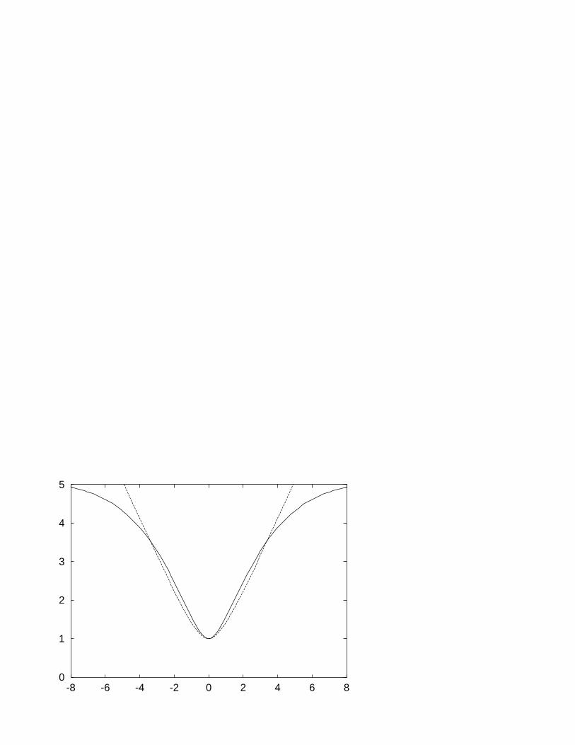
It has been well recognized and confirmed in many waysthat the front velocity is connected with the causality, andthecausality has no direct connection with the group velocity.Butone is still apt to connect the group velocity with the causalitybecause many practical communication systems utilize pulsemodulation to send information.
Let us examine our system shown in Fig. 13 in terms ofcausality. By pushing the switch (O), a rectangular pulse (A)is generated. Feeding it into the lowpass filter, a band-limitedpulse (B) is prepared. Finally sending it through the negativedelay circuit, an advanced pulse (C) is created. This would bea cause-effect chain in a casual sense. However the reversal ofthe chronological order between (B) and (C) causes the troublefor the naive picture. One may think that making use of thistwist it is possible to send information to the past despite of thecausality. Of course this is wrong.
First we should realize that in a strict sense all the pulses (A),(B), and (C) are causal to each other because they are the signalsin a single lumped system. When an impulse is applied to a qui-escent lumped system, then all parts respond instantaneously.Some of them look delayed, but they just started smoothly astk (k > 1). All the pulse fronts share the timet = 0, when theswitch is turned on (O). Therefore the above discussion on theorder is totally pointless.
But one may still shelve the theory, which deals with the al-most unseen signals just aftert = 0, considering practical situa-tion where the information is related to the peak position ortherising edge where a half of the pulse peak is reached. However,
in order to generate a smooth pulse (B) which is acceptable tothe negative delay circuit, we have to make a decision well inadvance (beforet = 0 in this case) because of the delay causedby the lowpass filter. Once we miss the timing, the numbermof the lowpass filters must be reduced in order to catch up. Butbreaking the conditionm > n, the pulse cannot be forwardedany more and is distorted badly.
Let us regard the negative delay circuit of Fig. 13 as a com-munication channel. We assign three people, Alice, Bob, andClare, on the sites (A), (B), and (C), respectively. Clare alwaysfinds a pulse before Bob does, i.e., she can always predict Bob’spulse. But Bob has no control over his pulses; he cannot cancela pulse initiated by Alice. The real sender of the pulse is notBob, but Alice. Bob is just an observer standing at the sendingsite. This scenario tells us that comparing the input and theout-put pulses of superluminal channel is somewhat nonsense andthat the real start point of the input pulse should be considered(See Sec. IV-C).
VIII. C
The negative group delay is already utilized in many prac-tical applications implicitly. Signals from slow sensors,suchas a hotwire anemometer, are compensated by a differentiatorwith a transfer function 1+ iωT. In PID (Proportional, Integral,and Derivative) controllers the derivative element (D) is used topredict the behavior of the system and to improve the dynami-cal response. When a capacitive load is connected to the outputof an operational amplifier, an additional feedback loop withderivative element is used, which is called lead compensations.All these efforts are to compensate delays in a system as far aspossible but the excessive use will result in instabilitiesor noiseproblems.
We have explored many aspects of negative delays and super-luminality utilizing circuit models. The use of circuit model isvery helpful because the choice of parameters are very flexibleand many handy circuit-simulation softwares are available. Ex-tension to nonlinear cases and to distributed systems [14] willbe very interesting.
One of the authors (MK) greatly appreciates stimulating andinspiring discussions with R. Chiao and all the participants ofthe mini program on Quantum Optics at the Institute of Theo-retical Physics, University of California Santa Barbara. He alsothanks K. Shimoda for informing about practical use of nega-tive delay circuits.
R[1] L. Brillouin, Wave Propagation and Group Velocity. New York: Aca-
demic Press, 1960, pp. 113–137.[2] S. Chu and S. Wong, “Linear pulse propagation in an absorbing medium,”
Phys. Rev. Lett., vol. 48, pp. 738–741, Mar. 1982.[3] R. Y. Chiao and A. M. Steinberg, “Tunneling times and superluminality”
Prog. Opt., vol. XXXVII, pp. 345–405, 1997.[4] G. Enders and G. Nimtz, “On the superluminal barrier traversal,”J. Phys.,
vol. I2, pp. 1693–1698, Sep. 1992.[5] A. M. Steinberg, P. G. Kwiat, and R. Y. Chiao, “Measurement of the
single-photon tunneling time,”Phys. Rev. Lett., vol. 71, pp. 708–711,Aug. 1993.
9
[6] M. W. Mitchell and R. Y. Chiao, “Causality and negative group delays ina simple bandpass amplifier,”Am. J. Phys., vol. 66, pp. 14–19, Jan. 1998.
[7] M. W. Mitchell and R. Y. Chiao, “Negative group delay and ‘fronts’ in acausal systems: An experiment with very low frequency bandpass ampli-fiers,” Phys. Lett., vol. A230, pp. 133–138, Jun. 1997.
[8] H. Cao, A. Dogariu, and L. J. Wang, “Negative group delay and pulsecompression in superluminal pulse propagation,” unpublished.
[9] L. J. Wang, A. Kuzmich, and A. Dogariu, “Gain-assisted superluminallight propagation,”Nature, vol. 406, pp. 277–279, Jul. 2000.
[10] A. Dogariu, A. Kuzmich, and L. J. Wang, “Transparent anomalous dis-persion and superluminal light-pulse propagation at a negative group ve-locity,” Phys. Rev. A, vol. 63, pp. 053806-1–11, Apr. 2001.
[11] T. Nakanishi, K. Sugiyama, and M. Kitano, “Demonstration of negativegroup delays in a simple electronic circuit,”Am. J. Phys., vol. 70, pp.1117–1121, Nov. 2002.
[12] U. Tietze and Ch. Schenk,Electronic Circuits. Verlin: Springer-Verlag,1991, pp. 350–408.
[13] P. Horowitz and W. Hill,The Art of Electronics,2nd Ed. Cambridge:Cambridge University Press, 1989, pp. 175–284.
[14] R. W. Ziolkowski, “Superluminal transmission of information through anelectromagnetic metamaterial,”Phys. Rev. E, vol. 63, pp. 046604-1–13,Apr. 2001.
0
1
2
3
4
5
-8 -6 -4 -2 0 2 4 6 8
Pulser LPF ( ) ND ( )
A B C
O
O
A BC
t
t = 0( )
nm
-0.4
-0.2
0
0.2
0.4
-8 -6 -4 -2 0 2 4 6 8
0
0.1
0.2
0.3
0.4
0.5
0.6
0 1 2 3 4 5 6 7