Embed Size (px)
Citation preview
1
Negative Capacitance in a Ferroelectric Capacitor Asif Islam Khan1, Korok Chatterjee1, Brian Wang1, Steven Drapcho2, Long You1, Claudy Serrao1, Saidur Rahman Bakaul1, Ramamoorthy Ramesh2,3,4, Sayeef Salahuddin1,4*
1 Dept. of Electrical Engineering and Computer Sciences, University of California, Berkeley 2 Dept. of Physics, University of California, Berkeley 3 Dept. of Material Science and Engineering, University of California, Berkeley 4 Material Science Division, Lawrence Berkeley National Laboratory, Berkeley, *To whom correspondence should be addressed; E-mail: [email protected]
The Boltzmann distribution of electrons poses a fundamental barrier to lowering energy
dissipation in conventional electronics, often termed as Boltzmann Tyranny1-5. Negative
capacitance in ferroelectric materials, which stems from the stored energy of phase
transition, could provide a solution, but a direct measurement of negative capacitance has so
far been elusive1-3. Here we report the observation of negative capacitance in a thin, epitaxial
ferroelectric film. When a voltage pulse is applied, the voltage across the ferroelectric
capacitor is found to be decreasing with time–in exactly the opposite direction to which
voltage for a regular capacitor should change. Analysis of this ‘inductance’-like behavior
from a capacitor presents an unprecedented insight into the intrinsic energy profile of the
ferroelectric material and could pave the way for completely new applications.
2
Owing to the energy barrier that forms during phase transition and separates the two degenerate
polarization states, a ferroelectric material could show negative differential capacitance while in
non-equilibrium1-5. The state of negative capacitance is unstable, but just as a series resistance
can stabilize the negative differential resistance of an Esaki diode, it is also possible to stabilize a
ferroelectric in the negative differential capacitance state by placing a series dielectric capacitor
1-3. In this configuration, the ferroelectric acts as a ‘transformer’ that boosts up the input voltage.
The resulting amplification could lower the voltage needed to operate a transistor below the limit
otherwise imposed by the Boltzmann distribution of electrons1-5. Due to this reason, the
possibility of a transistor that exploits negative differential capacitance has been widely studied
in the recent years6-13. However, despite the fact that negative differential capacitance has been
predicted by the standard Landau model going back to the early days of ferroelectricity14-18, a
direct measurement of this effect has never been reported, severely limiting the understanding
and potential application of this effect for electronics. In this work, we demonstrate the negative
differential capacitance in a thin, single crystalline ferroelectric film, by constructing a simple R-
C network and monitoring the voltage dynamics across the ferroelectric capacitor.
We start by noting that capacitance is, by definition, a small signal concept-capacitance C at a
given charge QF is related to the potential energy U by the relation C=[d2U/dQF2]-1. Due to this
reason we shall henceforth use the term ‘negative capacitance’ to refer to ‘negative differential
capacitance’. For a ferroelectric material, as shown in Fig. 1(a), the capacitance is negative only
in the barrier region around QF=0. Starting from an initial state P, as a voltage is applied across
the ferroelectric capacitor, the energy landscape is tilted and the polarization will move to the
nearest local minimum. Fig. 1(b) shows this transition for a voltage which is smaller than the

3
coercive voltage Vc. If the voltage is larger than Vc, one of the minima disappears and QF moves
to the remaining minimum of the energy landscape (Fig. 1(c)). Notably as the polarization rolls
downhill in Fig. 1(c), it passes through the region where C=[d2U/dQF2]-1 <0. Therefore, while
switching from one stable polarization to other, a ferroelectric material crosses through a region
where the differential capacitance is negative.
To experimentally demonstrate the above, we applied voltage pulses across a series combination
of a ferroelectric capacitor and a resistor R and observed the time dynamics of the ferroelectric
polarization. A 60 nm film of ferroelectric Pb(Zr0.2Ti0.8)O3 (PZT) was grown on metallic
SrRuO3 (60 nm) buffered SrTiO3 substrate using the pulsed laser deposition technique. Square
gold top electrodes with a surface area A= (30 µm)2 were patterned on top of the PZT films using
standard micro-fabrication techniques. The remnant polarization of the PZT film is measured to
be ~0.74 C/m2 and the coercive voltages are +2 V and -1.8 V. R = 50 kΩ is used as the series
resistor. Fig. 2(a) shows the schematic diagram of the experimental setup and Fig. 2(b) shows
the equivalent circuit diagram. The capacitor C connected in parallel with the ferroelectric
capacitor in Fig. 2(b) represents the parasitic capacitance contributed by the probe-station and the
oscilloscope in the experimental setup, which was measured to be ~60 pF. An AC voltage
pulse VS: -5.4 V→ +5.4 V → -5.4 V was applied as input. The total charge in the ferroelectric and
the parasitic capacitor at a given time t, Q(t), is calculated using 𝑄(𝑡) = 𝑖!(𝑡)𝑑𝑡!! , iR being the
current flowing through R. The charge across the ferroelectric capacitor QF(t) is calculated using
the relation: 𝑄! 𝑡 = 𝑄 𝑡 − 𝐶𝑉! 𝑡 , VF being the voltage measured across the ferroelectric
capacitor. Fig. 2(c) shows the transients corresponding to VS, VF , iR and Q. We note in Fig. 2(c)
that after the -5.4 V→ +5.4 V transition of VS, VF increases until point A, after which it decreases
4
till point B. We also note in Fig. 2(c) that during the same time segment, AB, iR is positive and Q
increases. In other words, during the time segment, AB, the changes in VF and Q have opposite
signs. As such, dQ/dVF is negative during AB which points to the fact that the ferroelectric
polarization is passing through the unstable negative states. A similar signature of negative
capacitance is observed after the +5.4 V → -5.4 V transition of VS during the time segment CD in
Fig. 2(c). The charge density of the ferroelectric capacitor or the ferroelectric polarization,
P(t)=QF(t)/A is plotted as a function of VF(t) in Fig. 3(a). We observe in Fig. 3(a) that the P(t)-
VF(t) curve is hysteretic and in the sections AB and CD, the slope of the curve is negative
indicating that the capacitance is negative in these regions.
We also experimented with AC voltage pulses of different amplitudes and two different values of
the series resistance. The P(t)-VF(t) characteristic is found to be qualitatively similar (see the
supplementary section 2 for detailed measurements). There are, however, some interesting
differences. For example, Fig. 3(b) compares the P(t)-VF(t) curves corresponding to R=50 kΩ
and 300 kΩ for VS: -5.4 V→ +5.4 V → -5.4 V. We note that for a smaller value of R, the
hysteresis loop is wider, which we will explain later.
We have simulated the experimental circuit shown in Fig. 2(b) starting from the Landau-
Khalatnikov equation14,
𝜌 !!!!"
= − !"!!!
; where energy density 𝑈 = 𝛼𝑄!! + 𝛽𝑄!! + 𝛾𝑄!! − 𝑄!𝑉!. (1)
α, β and γ are the anisotropy constants and ρ is a material dependent parameter that accounts for
dissipative processes during the ferroelectric switching. Equation (1) leads to an expression for
the voltage across the ferroelectric capacitor as:
5
𝑉! =!!
!!(!!)+ 𝜌 !!!
!" where 𝐶!(𝑄!) = (2𝛼𝑄! + 4𝛽𝑄!! + 6𝛾𝑄!!)!!. (2)
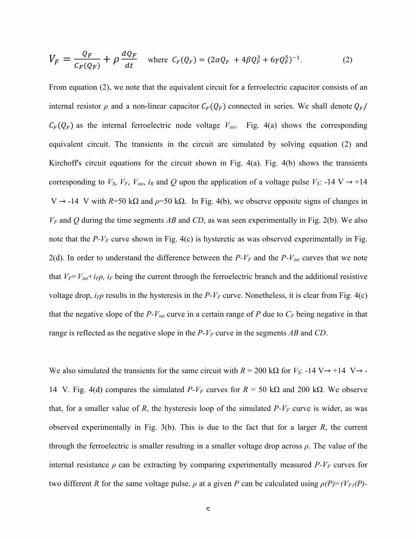
From equation (2), we note that the equivalent circuit for a ferroelectric capacitor consists of an
internal resistor ρ and a non-linear capacitor 𝐶!(𝑄!) connected in series. We shall denote 𝑄!/
𝐶!(𝑄!) as the internal ferroelectric node voltage Vint. Fig. 4(a) shows the corresponding
equivalent circuit. The transients in the circuit are simulated by solving equation (2) and
Kirchoff's circuit equations for the circuit shown in Fig. 4(a). Fig. 4(b) shows the transients
corresponding to VS, VF, Vint, iR and Q upon the application of a voltage pulse VS: -14 V → +14
V → -14 V with R=50 kΩ and ρ=50 kΩ. In Fig. 4(b), we observe opposite signs of changes in
VF and Q during the time segments AB and CD, as was seen experimentally in Fig. 2(b). We also
note that the P-VF curve shown in Fig. 4(c) is hysteretic as was observed experimentally in Fig.
2(d). In order to understand the difference between the P-VF and the P-Vint curves that we note
that VF=Vint+iFρ, iF being the current through the ferroelectric branch and the additional resistive
voltage drop, iFρ results in the hysteresis in the P-VF curve. Nonetheless, it is clear from Fig. 4(c)
that the negative slope of the P-Vint curve in a certain range of P due to CF being negative in that
range is reflected as the negative slope in the P-VF curve in the segments AB and CD.
We also simulated the transients for the same circuit with R = 200 kΩ for VS: -14 V→ +14 V→ -
14 V. Fig. 4(d) compares the simulated P-VF curves for R = 50 kΩ and 200 kΩ. We observe
that, for a smaller value of R, the hysteresis loop of the simulated P-VF curve is wider, as was
observed experimentally in Fig. 3(b). This is due to the fact that for a larger R, the current
through the ferroelectric is smaller resulting in a smaller voltage drop across ρ. The value of the
internal resistance ρ can be extracting by comparing experimentally measured P-VF curves for
two different R for the same voltage pulse. ρ at a given P can be calculated using ρ(P)=(VF1(P)-
6
VF2(P))/(iF1(P)-iF2(P)) where VF1(P) and VF2(P) are the ferroelectric voltages at a given P for two
R and iF1(P) and iF2(P) are the corresponding current through the ferroelectric at the same P. The
average ρ found to decrease monotonically with an increasing amplitude of the applied voltage,
while the average value of the negative capacitance remains reasonably constant (see
supplementary Fig. S17).
If the applied voltage amplitude is smaller than coercive voltage so that the ferroelectric resides
in one of the potential wells (see Fig 1a), its capacitance is positive and so it should behave just
as a simple capacitor. On the other hand, if the applied voltage amplitude is larger than the
coercive voltage, the ferroelectric switches and a negative capacitance transient is expected. This
is exactly what is observed in our experiments (see Supplementary section 4.3). The fact that in
the same circuit both positive and negative capacitance transients can be achieved just by
changing the amplitude of the voltage also indicate that any influence of the parasitic
components, if present, are minimal. In addition, detailed measurements (see Supplementary
section 3) show that influence of defects is also minimal. Furthermore, the observed effect is
robust against material variations. Supplementary section 8 shows data for a different material
stack where PZT thickness is increased to 100 nm and bottom electrode is changed to
La0.5Sr0.5MnO3 (20 nm) from SRO. A similar negative capacitance transient is observed.
The addition of a series resistance (R) is critically important to reveal the negative capacitance
region in the dynamics. An appreciable voltage drop across the series R makes sure that the
voltage across the ferroelectric capacitor can be measured without being completely dominated
by the source voltage–at the limit when R!0, the voltmeter would be directly connected across
7
the voltage source. Indeed, most model studies15,19-21 have been done in the latter limit where the
ferroelectric capacitor is directly connected across a voltage source (or through a small
resistance). Note that the dynamics in our experiments are intentionally slowed down by adding
a large series resistance. The duration of the negative capacitance transient can be probed by
varying the value of the series resistance and is found to be approximately 20 ns (see
Supplementary section 8).
A negative slope in the polarization-voltage characteristic has been predicted since the early days
of ferroelectricity14-18. A S-like polarization voltage behavior in one branch of the hysteresis was
measured in a transistor structure in Ref. 11. However, a successful measurement of the entire
intrinsic hysteresis loop has been performed only indirectly18. By contrast, our results provide a
direct measure of the intrinsic hysteresis and negative capacitance of the material. Given the size
of the capacitor used (30 µm x 30 µm), the switching invariably happens through domain-
mediated mechanisms. Importantly, our results show that, even in such a domain mediated
switching, a regime of abrupt switching is present that leads to negative capacitance transience.
Thus, the double well picture shown in Fig. 1(a) which is typically associated with a single
domain configuration (Eq. 1), can still qualitatively predict the experimental outcome.
Interestingly, from Fig. 2(c), it is clear that the negative capacitance ensues in the initial period
of the switching. This indicates that microscopically abrupt switching events dominate the early
part of the dynamics, thereby providing a unique insight into the switching process. By varying
external stimuli, it is also possible to probe the behavior of intrinsic parameters such as ρ (see
Supplementary Information Section 6) that govern the ferroelectric switching. Before
concluding, it is worth noting that the concept of negative capacitance goes beyond the

8
ferroelectric hysteresis and can be applied in general to a two state system separated by an
intrinsic barrier (stored energy)22-26. The measurement presented here could provide a generic
way to probe the intrinsic negative capacitance in all such systems. A robust measurement of the
negative capacitance could provide a guideline for stabilization which could then overcome
Boltzmann Tyranny in field effect transistors, as mentioned earlier. The inductance-like behavior
observed in this experiment could also lead to many other applications such as to negate
capacitances in an antenna, to boost up voltages at various part of a circuit, to develop coil-free
resonators and oscillators, etc.
Acknowledgements: This work was supported in part by FCRP Center for Materials, Structures
and Devices (MSD), the STARNET LEAST center, the NSF E3S center at Berkeley and Office
of Naval Research (ONR). A.I.K. acknowledges the Qualcomm Innovation Fellowship 2012-13.

9
References
1. Salahuddin, S., Datta & S. Use of negative capacitance to provide voltage amplification for low power nanoscale devices. Nano Lett. 8, 405-410 (2008).
2. Zhirnov, V. V. & Cavin, R. K. Negative capacitance to the rescue. Nature Nanotechnology 3, 77-78 (2008).
3. Theis, T. N. & Solomon, P. M. It’s time to reinvent the transistor! Science 327, 1600-1601
(2010). 4. Theis, T. N. & Solomon, P. M. In quest of the next switch: prospects for greatly reduced power
dissipation in a successor to the silicon field-effect transistor. Proc. IEEE 98, 2005-2014 (2010).
5. Ionescu, A. M. & Riel, H. Tunnel field-effect transistors as energy-efficient electronic switches, Nature 479, 329-337 (2011).
6. C. Dubourdieu et al. Switching of ferroelectric polarization in epitaxial BaTiO3 films on silicon
without a conducting bottom electrode. Nature Nanotech. 8, 748-754 (2013).
7. Salahuddin, S. & S. Datta, S. Proc. Intl. Electron Devices Meeting (IEDM), 2008.
8. Rusu, A., Salvatore, G. A., Jiménez, D., Ionescu, A. M. Metal-Ferroelectric-Metal-Oxide-Semiconductor Field Effect Transistor with Sub-60mV/decade Subthreshold Swing and Internal Voltage Amplification. Proc. Intl. Electron Devices Meeting (IEDM), 2010.
9. Khan A. I. et al. Experimental evidence of ferroelectric negative capacitance in nanoscale heterostructures Appl. Phys. Lett. 99, 113501-3 (2011).
10. Khan A. I. et. al. Ferroelectric negative capacitance MOSFET: capacitance tuning & antiferroelectric operation Proc. Intl. Electron Devices Meeting (IEDM), 2011.
11. Salvatore, G. A., Rusu, A. & Ionescu, A. M. Experimental confirmation of temperature dependent negative capacitance in ferroelectric field effect transistor. Appl. Phys. Lett. 100, 163504-1-3 (2012).
12. Then, H. W. et al. Experimental observation and physics of “negative” capacitance and steeper than 40mV/decade subthreshold swing in Al0.83In0.17N/AlN/GaN MOS-HEMT on SiC substrate. Proc. Intl. Electron Devices Meeting (IEDM), 2013.
13. The International Technology Roadmap for Semiconductors, Emerging Research Devices
(http://www.itrs.net/Links/2011itrs/home2011.htm, (2011).
14. Landau, L. D. & Khalatnikov, I. M. On the anomalous absorption of sound near a second order phase transition point. Dok. Akad. Nauk 96, 469-472 (1954).
15. Lines, M. E. & Glass, A. M. Oxford University press, 1977.
10
16. Merz, W. J. Switching time in ferroelectric BaTiO3 and its dependence on crystal thickness. J. of Appl. Phys. 27, 938-943 (1956).
17. Bratkovsky, A. M. & Levanyuk, A. P. Very large dielectric response of thin ferroelectric films with the dead layers. Phys. Rev. B 63, 132103-1-3 (2001).
18. Bratkovsky, A. M. & Levanyuk, A. P. Depolarizing field and “real” hysteresis loops in nanometer-scale ferroelectric films. Appl. Phys. Lett. 89, 253108-1-3 (2006).
19. Larsen, P. K. et al. Nanosecond switching of thin ferroelectric films. Appl. Phys. Lett. 59, 611-613 (1991).
20. Li, J. et al. Ultrafast polarization switching in thin-film ferroelectrics. Appl. Phys. Lett. 84, 1174-1176 (2004).
21. Jiang, A. Q. et al. Subpicosecond domain switching in discrete regions of Pb(Zr0.35Ti0.65)O3 thick
films. Adv. Func. Mat. 22, 2148-2153 (2012).
22. Jana, R. K., Snider, G. L. and Jena, D. On the possibility of sub 60 mV/decade subthreshold
switching in piezoelectric gate barrier transistors. Physica Status Solidi (c) 10, 1469-1472
(2013).
23. AbdelGhany, M. and Szkopek, T. Extreme sub-threshold swing in tunnelling relays. Appl. Phys.
Lett. 104, 013509 (2014).
24. Masuduzzaman, M., and Alam, M. A. "Effective Nanometer Airgap of NEMS Devices using Negative Capacitance of Ferroelectric Materials." Nano Lett. 14, 3160–3165 (2014).
25. Eisenstein, J. P., L. N. Pfeiffer, and K. W. West. "Negative compressibility of interacting two-
dimensional electron and quasiparticle gases." Phys. Rev. Lett. 68, 674-677 (1992).
26. Li, Lu, et al. "Very large capacitance enhancement in a two-dimensional electron system." Science 332, 825-828 (2011).
11
Figure 1: Energy Landscape description of the ferroelectric negative capacitance. (a) The
energy landscape of a ferroelectric capacitor in the absence of an applied voltage. The
capacitance is negative only in the barrier region around QF=0. (b,c) The evolution of the energy
landscape upon the application of a voltage across the ferroelectric capacitor that is smaller (b)
and larger than the coercive voltage (c). If the voltage is larger than the coercive voltage, the
ferroelectric polarization rolls down hill through the negative capacitance states.
U (a
.u.)
QF (a.u.)
C<0 C>0C>0 C<0
U (a
.u.)
QF (a.u.)
Time
Volta
ge a
cros
s Fe
rroel
ectri
c
QF =0 QF =0
0
(a) (b) (c)
P
U (a
.u.)
QF (a.u.)
C<0
QF =0
P
Q
Q
R
Coercive voltage Vc

12
Figure 2: Transient response of a Ferroelectric Capacitor. (a) Schematic diagram of the
experimental setup. (b) Equivalent circuit diagram of the experimental setup. (c) Transients
corresponding to the source voltage VS, the ferroelectric voltage VF and the charge Q upon the
application of a AC voltage pulse VS: -5.4 V→ +5.4 V → -5.4 V. R=50 kΩ.
Chan
nel 2
(VF)
+
-
+
-
Chan
nel 1
(V S)
CF
R
Vs
+
iR
C
(b)
−6
−4
−2
0
2
4
6
−80−60−40−20
02040
0 20 40 60 80 100−1
−0.5
0
0.5
1
t (μs)
Volta
ge (V
)i R
(μA)
Q (n
C)
0 10 20 30 403
3.2
3.4
3.6
3.8
4
65 70 75 80 85−1.8
−1.7
−1.6
−1.5
−1.4
−1.3
−1.2
−1.1
−1t (μs)
t (μs)
V F (V
)V F
(V)
A B
C D
(b)(a)
(c)
A B
C D
Agile
nt 8
1150
A pu
lse
func
tion
gene
rato
r
R=50 kΩ
VF
-
13
Figure 3: Experimental measurement of Negative Capacitance. (a) The ferroelectric
polarization P(t) as a function of VF(t) with R=50 kΩ for VS: -5.4 V→ +5.4 V → -5.4 V. (b)
Comparison of the P(t)-VF(t) curves corresponding to R=50 kΩ and 300 kΩ for VS: -5.4 V→
+5.4 V → -5.4 V.
−3 −2.5 −2 −1.5
−0.5
0
0.5
3 3.5 4 4.5 5 5.5 6−0.8−0.6−0.4−0.2
00.20.40.60.8
−6 −4 −2 0 2 4 6−1
−0.5
0
0.5
1
VF (V)
P (C
/m2 )
VF (V)VF (V)
P (C
/m2 )
P (C
/m2 )
−6 −4 −2 0 2 4 6−1
−0.5
0
0.5
1
VF (V)
P (C
/m2 )
R=50 kΩR=300 kΩ
R=50 kΩ(a)
(b)
14
Figure 4: Simulation of the time-dynamics of the ferroelectric switching. (a) Equivalent
circuit diagram of the simulation. (b) Simulated transients corresponding to the source voltage
VS, the ferroelectric voltage VF and the charge Q upon the application of a voltage pulse VS: -14
V→ +14 V → -14 V. (c) The ferroelectric polarization P(t) as a function of VF(t) and Vint(t). (d)
Comparison of the simulated P(t)- VF(t) curves for R = 50 kΩ and 200 kΩ upon the application
of VS: -14 V → +14 V → -14 V.
−20 0 20−1
−0.5
0
0.5
1
P-Vint
P-VF
A
BC
D
−10
0
10
200
0
200
0 20 40 60 80−2−1
01
Volta
ge (V
)Q
(nC
)
t (μs)
P (C
/m2 )
Voltage (V)
A B CD
C D
(b)
(c)
Vs Vint VF
(a)
R
CF(QF)
ρVs
+
iR
+
C
Ferro
elec
tric iF
i R (μ
A)
8 V14 V
−20 0 20−1
−0.5
0
0.5
1
VF (V)
P (C
/m2 )
(d)
R=300 kΩR=50 kΩ
R=50 kΩ
iC
+ + - VF
Vint- -

1
Supplementary Online Information: Negative Capacitance in a Ferroelectric Capacitor
Asif Islam Khan,1 Korok Chatterjee,1 Brian Wang,1 Steven Drapcho,2
Long You,1, Claudy Serrao,1, Saidur Rahman Bakaul,1, Ramamoorthy Ramesh,2,3,4 Sayeef Salahuddin1,4∗
1Dept. of Electrical Engineering and Computer Sciences, University of California, 2Dept. of Physics, University of California,
3Dept. of Material Science and Engineering, University of California, 4Material Science Division, Lawrence Berkeley National Laboratory Berkeley, CA 94720
∗To whom correspondence should be addressed; E-mail: [email protected]
1 Growth and structural characterization A 60 nm Pb(Zr0.2 Ti0.8)O3 (PZT) thin film was grown on a 60 nm metallic SrRuO3 (SRO)
buffered SrTiO3 (STO) substrate using the pulsed laser deposition technique. PZT, SRO and
STO are closely lattice matched, for which the epitaxial growth of the heterostructure results in
a high crystalline quality and a robust ferroelectricity in PZT and minimizes defects. SRO and
PZT films were grown at 630 0C and 720 0C respectively. During the growth, the oxygen partial
pressure was kept at 100 mTorr and afterwards the heterostructure was slowly cooled down at 1
atm of oxygen partial pressure and a rate of -5 0 C/min to the room temperature. Laser pulses of
100 mJ of energy and ~∼4mm2 of spot size were used to ablate the targets. Gold top electrodes
were ex-situ deposited by e-beam evaporation and then patterned using standard lithographic
techniques into square dots of a surface area, A= (30 µm)2 . The SRO layer was used as the bot-

2
) . u a t y i tn e I n
x Inte
nsity
(a.u
) s
(
Q (
1/Å)
z
(a)
(b)
100
10−2
10−4
10−6
1 0.8
STO (002) SRO (002)
PZT (002) 42 43 44 45 46 47
2θ (0)
(c)
0.78
0.77
0.76
0.75
0.74
0.73
STO (103) SRO (103)
PZT (103)
0.6
0.72
0.4
0.2
0
PZT (002)
0.71
0.23 0.24 0.25 0.26 0.27 0.28
Q (1/Å) −0.5 0 0.5
Δω (0) Figure S1: (a) The X-ray diffraction spectrum of the PZT(60 nm)/SRO(60nm) heterostructure on the STO substrate around the (002) reflections. (b) The rocking curve measurement around the PZT (002) reflection. (c) The reciprocal space map of the heterostructure around the (103) reflections of the heterostructure.
tom electrode. The chosen thicknesses of PZT and SRO ensure a very low leakage and a good
bottom contact. Fig. S1(a) shows the X-ray diffraction spectrum of the heterostructure around
the (002) reflections. Fig. S1(b) shows the rocking curve measurement around the PZT (002)
reflection. The full-width-at-the-half-maximum of the PZT (002) peak, ∆ω, is ~∼0.10. Fig.
S1(c) shows the reciprocal space map of the heterostructure around the (103) reflections. We
note that the PZT (103) peak has a smaller Qx than that of the substrate (103) peak indicating
that the PZT film is partially/fully strain relaxed.
2 Measurement of the remnant polarization The ferroelectric hysteresis loop is traditionally measured using the Sawyer-Tower technique
(1). Fig. S2(a) shows the ferroelectric hysteresis loop of the 60 nm PZT film grown on SRO
buffered STO (001) substrate measured by this technique using a Radiant Precision Multiferroic
tester. To supplement the Sawyer-Tower measurement of the remnant polarization, we also
3
P (µ
C/c
m2 )
2ΔP
(µC
/cm
2 )
(a) 73.5
50
(b) 300 200
100
0 0
−50
−75.5
−6 −4 −2 0 2 4
V (V)
−100 −200 −300
0 1 2 3 4 5 V (V)
Figure S2: (a) The polarization (P )-voltage (V ) hysteresis curve of the ferroelectric measured using a Sawyer-Tower type setup. (b) The positive-up-negative-down (PUND) measurement of the PZT capacitor.
measured the switched polarization using the positive-up-negative-down (PUND) technique,
which is usually used to distinguish between ferroelectric switching and artifacts caused by
defects (2). Fig. S2(b) shows the positive-up-negative-down (PUND) measurement of the PZT
capacitor. The remnant polarization as measured using both of the techniques are the same
(~∼0.74 C/m2) indicating that defects play a minimal role in determining the properties of our
sample.
3 Dielectric characterization and frequency dispersion
Fig. S3(a, b, c, d) show the dielectric constant-voltage and the admittance angle-voltage char-
acteristics of the PZT sample at 1 kHz, 10 kHz, 100 kHz and 1 MHz respectively and fig.
S3(e) shows the frequency dispersion of the dielectric constant between 1 kHz and 1 MHz. In
fig. S3(a-e), we observe that the admittance angle is ~∼900 at all frequencies. This points to
negligible DC leakage through our samples. We further note in fig. S3(e) that the dispersion
of the dielectric constant over 3 orders of magnitude variation in frequency is less than 5%.
Generally, the defect dynamics that include trapping of electrons and charging/discharging of
the same in the defect states result in large frequency dispersion of the dielectric constant in
4
(e)
Die
lect
ric
Con
stan
t A
dmitt
ance
A
ngle
(0 )
D
iele
ctric
C
onst
ant
Adm
ittan
ce
Ang
le (
0 )
Die
lect
ric
Con
stan
t A
dmitt
ance
A
ngle
(0 )
Die
lect
ric
Con
stan
t A
dmitt
ance
A
ngle
(0 )
Die
lect
ric
Con
stan
t A
dmitt
ance
A
ngle
(0 )
(a) f= 1 kHz
80 (b)
f= 10 kHz f= 100 kHz f= 1 MHz (c) (d)
60
40
20
90
60
30
0 −2 0 2 4
60 40 20 90
60
30
0 −2 0 2 4
60 40 20 90
60
30
0 −2 0 2 4
60 40 20 90
60
30
0 −2 0 2 4
(e)
Voltage (V) 50 40 30 20 10
Voltage (V) Voltage (V) Voltage (V)
90 60 30
0 100 101 102 103
Frequency (kHz) Figure S3: (a,b,c,d) Dielectric constant-voltage and the admittance angle-voltage characteristics of the PZT sample at 1 kHz (a), 10 kHz (b), 100 kHz (c) and 1 MHz (d) . (e) The frequency dispersion of the dielectric constant between 1 kHz and 1 MHz
ferroelectrics (3). This points to the fact there is a negligible amount of defects in the PZT
sample.
Another technique that is widely used to characterize the defects in ferroelectrics is the
Rayleigh analysis (3–5). The basis of this analysis is that, due to the movement of the defects
in response to an AC electric field E0, the dielectric constant of a ferroelectric increases as E0
increases even when E0 is smaller the coercive field. Fig. S4 shows the dielectric constant εr
as a function the AC electric field E0 at 10 kHz. We observe that as the AC electric field is
increased from 10 kV/cm to the coercive field (~∼250 kV/cm), the dielectric constant increases
by a mere 1.5%. This independently shows that the defects are minimal for our PZT sample.

5
Die
lect
ric C
onst
ant
50
40
30
20
10
0 50 100 150 200 250
Electric field (kV/cm)
Figure S4: The dielectric constant εr as a function the AC electric field E0 at 10 kHz. 4 Transient response of the ferroelectric capacitor 4.1 Experimental setup for measuring the transient response
The PZT capacitor was connected to a voltage pulse source (Agilent 81150A pulse function
generator) through an external series resistor R. The voltage transients were measured using a
digital storage oscilloscope (Tektronix 2024). Top Au and bottom SRO contacts were connected
to the probe tips in a probe station through which the ferroelectric capacitor was connected to
the other circuit components. Main text fig. 2(a) shows the experimental setup and the electrical
connections to the oscilloscope.
4.2 Extraction of the parasitic capacitance
In order to extract the value of the parasitic capacitance which is referred to as C in main text
fig. 2(b), voltage pulses were applied across the probe station under open circuit conditions
through the resistor R = 50 kΩ. Fig. S5(a) shows the transient response of the circuit for an
applied voltage Vs : -5.4 V→+5.4 V. By fitting the voltage transient across the probes Vx shown
in Fig. S5(a) to the equation Vx(t) = (+5.4 − 2 × 5.4e−t/(RC ) ) V with R = 50 kΩ, the value of
the parasitic capacitance C is extracted to be ~∼60 pF. Fig. S5(c) compares the transients of the
6
V V
C
+ V -
x
Q (n
C)
Q (n
C)
Volta
ge (V
)
i (µ
A)
R
Q (n
C)
Volta
ge (V
)
Appl
ied
Volta
ge
(a)
5
0
R V i +Q
(c)
5 s R
-Q
−5
0.4 s x
0.2
0
−0.2
0
Voltage between the probes
Solid Curve: w/ FE −5 Dotted Curve: w/o FE 40 20
0
(b)
−0.4
0.4
0 20 40 2
t (µs)
1
0.2
0
−0.2
0
0 20 40 t (µs)
−0.4 −5 0 5
Voltage (V) Figure S5: (a) Transient response of the circuit under the open circuit conditions to an AC volt- age pulse Vs : -5.4 V →+5.4 V. (b) The charge-voltage characteristics of the parasitic capacitor. (c) Comparison of the transients for the circuit under an open circuit condition with those in the closed circuit with the ferroelectric capacitor between the probes for an AC voltage pulse Vs : -5.4 V →+5.4 V.
open circuit with those of the closed circuit with the ferroelectric capacitor connected between
the probes in response an AC voltage pulse Vs : -5.4 V→+5.4 V. In Fig. S5(c), we observe that,
after the transition of Vs , the transients are initially dominated by the parallel capacitor, which
is corroborated by simulations.
7
4.3 Correlation between the ferroelectric switching and the negative ca-
pacitance transient
To correlate the characteristic negative capacitance transients with the ferroelectric switching,
we note the following.
1. When a voltage is applied which is lower than the coercive voltage so that there is no
switching of the polarization, we observe simply a capacitive charging of the voltage,
as expected from the double well energy landscape of the ferroelectric material. The
coercive voltage of our PZT sample is ±2 V, which is evident from the hysteresis loop
plotted in Fig. S2(a). In Fig. S6(a,b), the voltage transients are shown for voltages pulses
Vs : -1 V→ +1 V → -1 V and Vs : -1.8 V→ +1.8 V → -1.8 V respectively. Clearly, there
are no negative capacitance transients observed in Fig. S6, since the applied AC voltage
amplitude is less the coercive voltage.
2. Now, in the same setup, when a voltage is applied which is larger than the coercive volt-
age so that the ferroelectric polarization switches its direction, we observe the negative
capacitance transient. In Fig. S7, the AC voltage magnitude is larger than the coercive
voltage and the negative capacitance transients are observed.
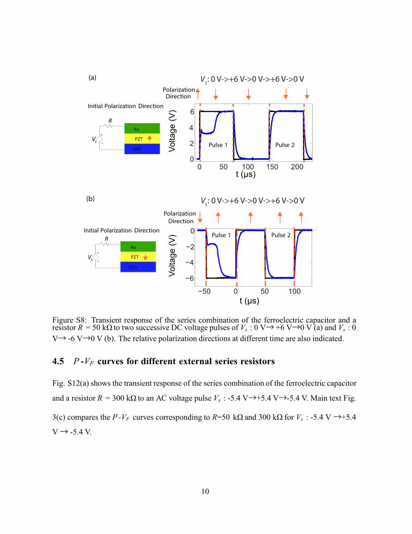
3. To further elucidate the point, we applied successive DC pulses on the PZT sample. In
Fig. S8(a), a large negative voltage pulse was first applied to align the polarization away
from the PZT/SRO interface and then two successive +6 V pulses were applied. We note
in Fig. S8(a) that during the 1st pulse, the switching of polarization occurs which results
in the characteristic negative capacitance transient of the ferroelectric voltage VF ; on the
other hand, during the 2nd pulse, the polarization does not switch since it had already been
aligned with the applied electric field in the previous pulse, and no negative capacitance
transient is observed in the VF waveform during the 2nd pulse. Similar experiment with

8
S
Volta
ge (V
) Vo
ltage
(V)
Volta
ge (V
) Vo
ltage
(V)
Volta
ge (V
) Vo
ltage
(V)
0
0 V
(a) VS: -1 V->+1 V->-1 V
2
1.5
1
0.5
R=50 kΩ 2
V S
V F V
S
V F
0
−0.5
−2 0 5 10 15 20
t (µs)
2
V S
V −1 0
F
(b)
−1.5 −2
0 5000 10000 t (µs)
V : -1.8 V->+1.8 V->-1.8 V
−2
5000 5005 5010 5015 5020 t (µs)
2
1.5
1
0.5
0
2
0 V S
V F
−2
0 5 10 15 20 t (µs)
−0.5
−1
−1.5
2
V S
V F
S
V F
R=50 kΩ −2
−2
0 5000 10000 t (µs)
5000 5005 5010 5015 5020 t (µs)
Figure S6: Transient response of the series combination of the ferroelectric capacitor and a resistor R = 50 kΩ to an AC voltage pulse Vs :-1 V→+1 V→-1 V (a) and Vs :-1.8 V→+1.8 V→-1.8 V (b).
two successive -6 V pulses is shown in Fig. S8(b).
This correlation between switching and the characteristic transients clearly shows that the
characteristic negative capacitance transients are due to the intrinsic ferroelectric switching dy-
namics and not because of any extrinsic defect dynamics.
9
Volta
ge (V
)
Volta
ge (V
) Vo
ltage
(V)
V : -3 V->+3 V->-3 V S
4
3 3
2 2.8
1
0
−1
−2
−3 V S
R=50 kΩ V F
2.6
0 100 200 300 t (µs)
−1.2 −1.4 −1.6
−4 0 200 400 600 800
t (µs)
−1.8 600 650 700
t (µs) Figure S7: Transient response of the series combination of the ferroelectric capacitor and a resistor R = 50 kΩ to an AC voltage pulse Vs :-3 V→+3 V→-3 V.
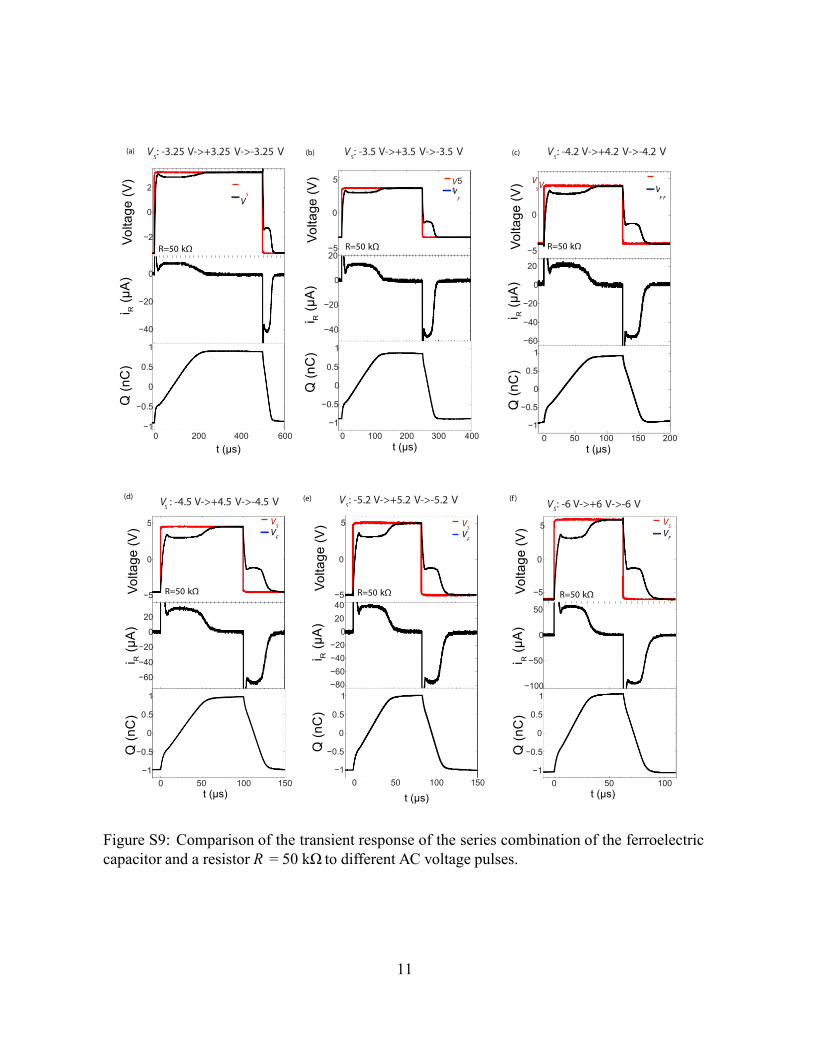
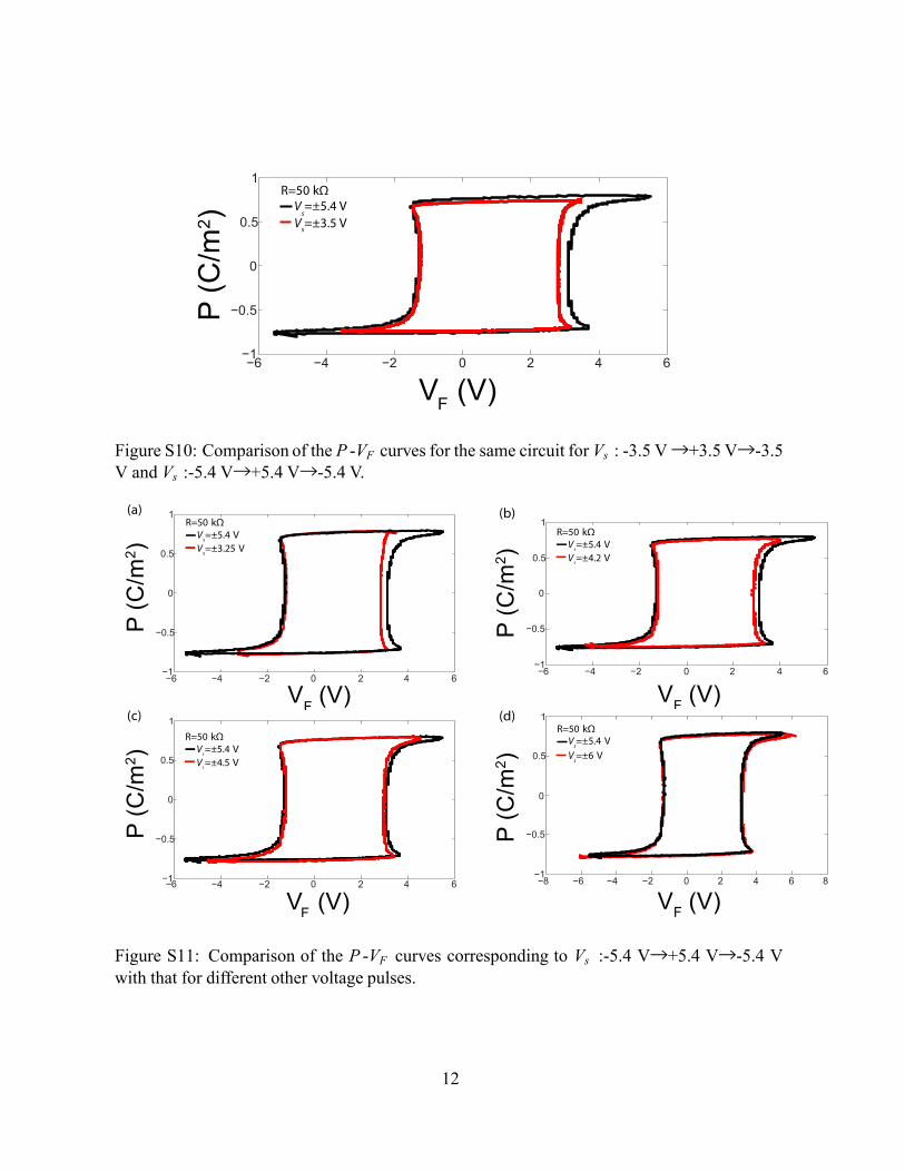
4.4 P -VF curves for different voltage amplitudes
Fig. S9(a,b,c,d,e) show the transient response of the series combination of the ferroelectric
capacitor and a resistor R = 50 kΩ to AC voltage pulses with amplitudes of 3.25 V, 3.5 V, 4.2 V,
4.5 V, 5.2 V and 6 V, respectively. Fig. S10 compares the P -VF curves of the same circuit for
Vs : -3.5 V →+3.5 V → -3.5 V and Vs :-5.4 V →+5.4 V →-5.4 V. Fig. S11 compares the P -VF
curve corresponding to Vs :-3.5 V→+3.5 V→-3.5 V with that for different other AC voltage
pulses. We note in Fig. S10 and S11 that for a larger peak voltage, the hysteresis window
is wider. This is due to the fact that for a larger peak voltage, a larger current flows into the
ferroelectric, thereby increasing the voltage drop across the internal resistance ρ.
10
S
S
Volta
ge (V
) Vo
ltage
(V)
(a) Polarization
Direction
V : 0 V->+6 V->0 V->+6 V->0 V
Initial Polarization Direction 6
R Au 4
+
V PZT S -
SRO
2 Pulse 1 Pulse 2 0
0 50 100 150 200 t (µs)
(b)
Initial Polarization Direction R
Au
Polarization
Direction
0
−2
V : 0 V->+6 V->0 V->+6 V->0 V
Pulse 1 Pulse 2
+
V PZT S -
SRO
−4 −6
−50 0 50 100 t (µs)
Figure S8: Transient response of the series combination of the ferroelectric capacitor and a resistor R = 50 kΩ to two successive DC voltage pulses of Vs : 0 V→ +6 V→0 V (a) and Vs : 0 V→ -6 V→0 V (b). The relative polarization directions at different time are also indicated.
4.5 P -VF curves for different external series resistors
Fig. S12(a) shows the transient response of the series combination of the ferroelectric capacitor
and a resistor R = 300 kΩ to an AC voltage pulse Vs : -5.4 V→+5.4 V→-5.4 V. Main text Fig.
3(c) compares the P -VF curves corresponding to R=50 kΩ and 300 kΩ for Vs : -5.4 V →+5.4
V → -5.4 V.
11
S S S
S S S
Q (n
C)
i (µ
A)
R
Volta
ge (V
) i
(µA
) R
Q
(nC
) Vo
ltage
(V)
i (µ
A)
R
Q (n
C)
Volta
ge (V
) Q
(nC
) i
(µA
) R
Vo
ltage
(V)
Q (n
C)
i (µ
A)
R
Volta
ge (V
) Q
(nC
) i
(µA
) Vo
ltage
(V)
R
2 V V
5
(a) V : -3.25 V->+3.25 V->-3.25 V (b) V : -3.5 V->+3.5 V->-3.5 V
(c) V : -4.2 V->+4.2 V->-4.2 V
5 V 5 V V S S
S
V F F F
0 0 0
−2
0
−20
R=50 kΩ
−5 20
0 −20
R=50 kΩ
−5
20
0 −20
R=50 kΩ
−40
1
0.5
0
−0.5
−1
0 200 400 600
t (µs)
−40
1
0.5
0 −0.5 −1
0 100 200 300 400
t (µs)
−40 −60
1
0.5
0 −0.5 −1
0 50 100 150 200
t (µs)
(d) V : -4.5 V->+4.5 V->-4.5 V
V S
V F
(e) V : -5.2 V->+5.2 V->-5.2 V 5 V
S
V F
(f )
V : -6 V->+6 V->-6 V
5 VS
V F
0 0 0
−5
20
0
−20
−40
−60
1
R=50 kΩ −5 40 20
0 −20 −40 −60 −80
1
R=50 kΩ −5
50
0
−50
−100
1
R=50 kΩ
0.5
0.5
0.5
0 0 0
−0.5
−0.5
−0.5
−1
0 50 100 150 t (µs)
−1
0 50 100 150
t (µs)
−1
0 50 100 t (µs)
Figure S9: Comparison of the transient response of the series combination of the ferroelectric capacitor and a resistor R = 50 kΩ to different AC voltage pulses.
12
s
s s
s
s
s
P (C
/m2 )
P
(C/m
2 )
P (C
/m2 )
P (C
/m2 )
P
(C/m
2 )
F
F F
F F
1
0.5
R=50 kΩ
V =±5.4 V s
V =±3.5 V s
0
−0.5
−1 −6 −4 −2 0 2 4 6
V (V) Figure S10: Comparison of the P -VF curves for the same circuit for Vs : -3.5 V →+3.5 V→-3.5 V and Vs :-5.4 V→+5.4 V→-5.4 V.
(a) 1
0.5
R=50 kΩ
V =±5.4 V V =±3.25 V
(b) 1
0.5
R=50 kΩ
V =±5.4 V V =±4.2 V
0 0
−0.5 −0.5
−1 −6 −4 −2 0 2 4 6
−1 −6 −4 −2 0 2 4 6
(c)
1 0.5
R=50 kΩ
V =±5.4 V V =±4.5 V
V (V) (d)
1 0.5
R=50 kΩ
Vs=±5.4 V Vs=±6 V
V (V)
0 0
−0.5 −0.5
−1 −6 −4 −2 0 2 4 6
−1 −8 −6 −4 −2 0 2 4 6 8
V (V) V (V) Figure S11: Comparison of the P -VF curves corresponding to Vs :-5.4 V→+5.4 V→-5.4 V with that for different other voltage pulses.

13
i (µ
A)
R
Q (n
C)
Volta
ge (
V)
V : -5.4 V->+5.4 V->-5.4 V S
5
0
−5 R=300 kΩ 10
0
−10
1
0
−1 0 200 400 600 800
t (µs) Figure S12: Transient response of the series combination of the ferroelectric capacitor and a resistor R = 300 kΩ to an AC voltage pulse Vs :-5.4 V→+5.4 V→-5.4 V. 5 Model 5.1 Anisotropy constants
For an applied electric field E across the ferroelectric capacitor, the per unit volume energy of
a ferroelectric Upu is given by
Upu = α1P 2 + α11 P 4 + α111 P 6 − P E (1)
where P is the surface charge density or the ferroelectric polarization and α1, α11 and α111 are
the anisotropy constants of the material. For a parallel plate capacitor of area A and thickness d,
the charge QF is given by QF = P A. The voltage across the ferroelectric capacitor VF = Ed
and the free energy of the capacitor U = Upu Ad. Hence the energy of the capacitor can be
14
1 A
Q Q Q
written as
U = Upu Ad
= {α ( QF
)2
+ α ( Q F )4
11 A
+ α ( QF
)6 111 A
QF − ( A )E}Ad
= dα1 2 A F
+
dα11 4 A3 F
+
dα111 6 A5 F
− QF VF (2)
Comparing equation (2) with the main text equation (1), the following relationships are
obtained.
α = dα1 A
β = dα11 A3
(3) (4)
γ = dα111 A5
(5)
The values of the anisotropy constants (α1, α11 and α111 ) are taken from Ref. (2).
5.2 Landau-Khalatnikov simulations
The circuit diagram for the simulation is shown in main text Fig. 4(a). A 60 nm PZT film
with square electrodes of area A= (30 µm)2 is taken as the ferroelectric capacitor. The parasitic
capacitance C =60 pF. ρ is taken as 50 kΩ. The remnant polarization corresponding to these
anisotropy constants is ~∼0.7 C/m2 and the coercive voltage is ±7.5 V.
The circuit shown in main text Fig. 4(a) is simulated by solving the following equations at
each time step.
0 = Vs (t) − iR (t)R − (iR (t) − iC (t))ρ − Vint (t) (6)

15
C
1 0 = Vint (t) + (iR (t) − iC (t))ρ − C
t
iC (t)dt (7)
QF (t) = QF (t = 0) + t=0
(iR (t) − iC (t))dt (8) QF (t) 3 5
Vint (t) =
CF (QF = 2αQF (t) + 4βQF + 6γQF (9)
(t))
VF (t) is calculated using the relation: VF (t) = Vint (t) + (iR (t) − iC (t))ρ.
Main text Fig. 4(b) shows the simulated transient response of the series combination of
the ferroelectric capacitor and a resistor R = 50 kΩ to an AC voltage pulse Vs : -14 V →+14
V → -14 V. The simulated transient response of the same circuit with R = 200 kΩ to an AC
voltage pulse Vs : -14 V →+14 V → -14 V is shown in Fig. S13. Main text Fig. 3(d) shows the
comparison between the simulated P − VF curves for R = 50 kΩ and 200 kΩ.
Although the model presented here describes a single domain scenario, the negative capac-
itance effect is equally applicable to ferroelectric switching that occurs through nucleation and
growth of domains. As long as there is a threshold and subsequent abrupt switching, a nega-
tive capacitance effect will ensue. The single domain picture tries to capture the threshold by
estimating it through a double-well energy profile and as such provides the mean value of the
microscopic parameters.
5.3 Estimation of ρ
The main text equation (2) can be rewritten as follows.
QF (t) VF (QF (t)) = F
(QF + ρiF (t) (10)
(t))
where iF = dQF /dt. Let us compare the dynamics of a ferroelectric capacitor for two different
resistors R1 and R2 for the same applied voltage pulse. Let t1 and t2 be the time variables for
these two cases, iF 1 and iF 2 be the corresponding currents through the ferroelectric capacitor
and VF 1 and VF 2 be the measured ferroelectric voltages for the resistors R1 and R2 respectively.

16
i (µ
A)
R
Q (n
C)
Volta
ge (V
)
10
0
−10 200
0
200
1
R=300 kΩ
0
−1
−2 0 200 400
t (µs) Figure S13: The simulated transient response of the series combination of the ferroelectric capacitor and a resistor R = 200 kΩ to an AC voltage pulse Vs :-14 V→+14 V→-14 V.
Hence,
QF 1 (t1) VF 1(QF 1(t1)) =
CF (QF 1 + ρiF 1(t1) (11)
(t1 )) QF 2 (t2) VF 2(QF 2(t2)) =
CF (QF 2 + ρiF 2(t2) (12)
(t2 ))
Let us assume that, in the first experiment with the resistor R1, QF 1 reaches a given value Q at t1 = τ1, and in the second experiment with R2 , QF 2 reaches Q at t2 = τ2 (i.e. QF 1 (t1 =
τ1) = QF 2 (t2 = τ2 ) = Q). Hence from equation (11) and (12), the following equation for ρ can

17
be derived.
ρ(Q) = VF 1(t1 = τ1) − VF 2(t2 = τ2) iF 1(t1 = τ1) − iF 2(t2 = τ2)
= VF 1 (Q) − VF 2(Q) iF 1 (Q) − iF 2(Q)
(13)
6 Dependence of ρ and the negative capacitance on the volt-
age amplitude
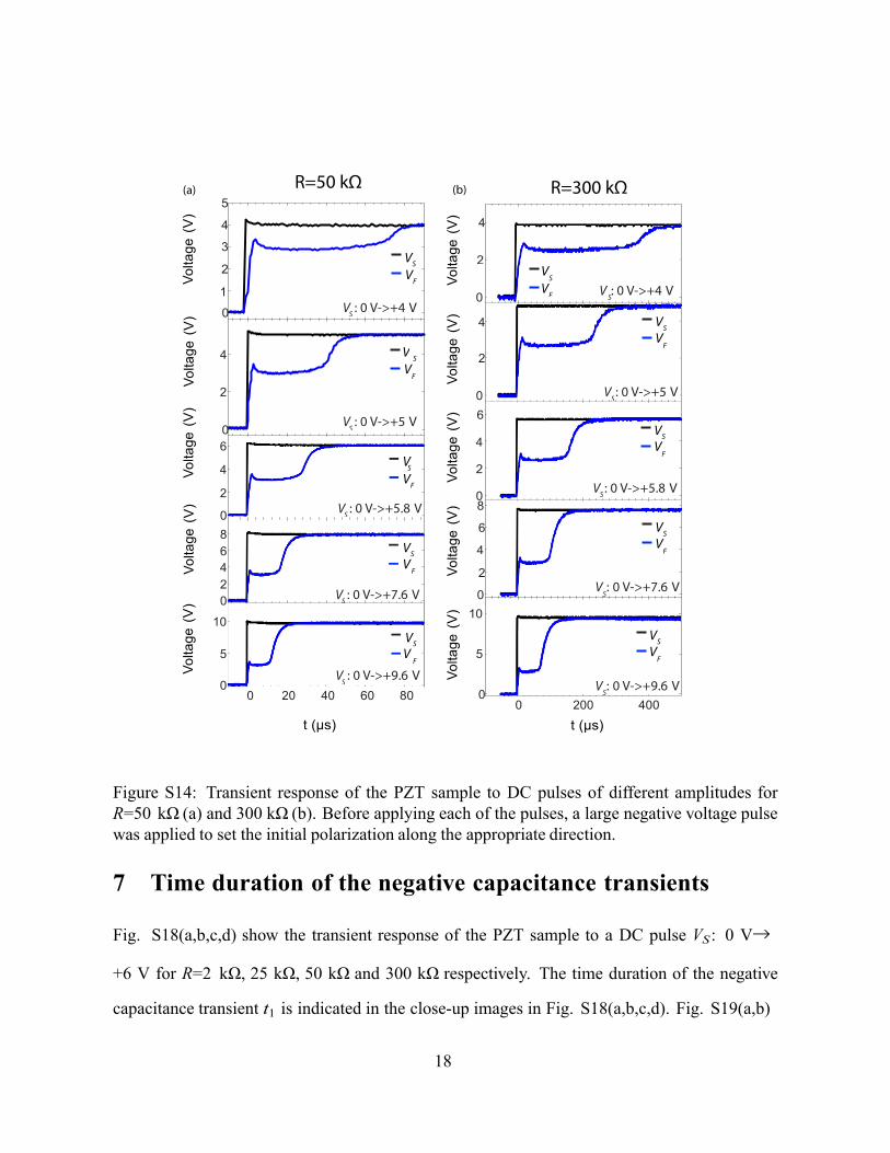
Fig. S14(a,b) show the transient response of the PZT sample to DC pulses of different applied
voltage amplitudes for R=50 kΩ and 300 kΩ respectively. Before applying each of the pulses
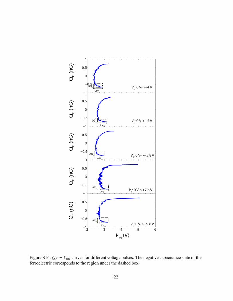
shown in Fig. S14, a large negative voltage pulse was applied to set the initial polarization along
the appropriate direction. Fig. S15(a,b) show the QF − VF and QF − iF curves respectively
for different applied voltage amplitudes with R= 50 kΩ and R= 300 kΩ. Fig. S15(c) shows
the value of ρ calculated using equation 13 as a function of QF for different voltage ampli-
tudes. Using the extracted value of ρ for a given voltage amplitude, the internal node voltage
Vint (QF (t)) = QF (t)/CF (QF (t)) = VF (QF (t)) − iF (QF (t)) × ρ is calculated. Fig. S16
shows the corresponding QF − Vint curves. In Fig. S16, the negative capacitance state of the
ferroelectric corresponds to the region under the dashed box. The average value of the negative
capacitance CF E is calculated using the equation: CF E = ∆QF /∆Vint , ∆QF and ∆Vint being
the changes in the ferroelectric charge and the internal ferroelectric node voltage in the negative
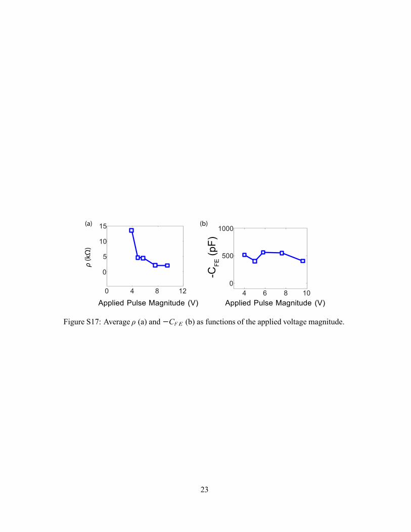
capacitance region, respectively. Fig. S17(a,b) plot the average ρ and −CF E respectively as
functions of the applied voltage amplitude. We note in fig. S17(a) that ρ decreases monoton-
ically with an increasing amplitude while CF E remains reasonably constant. Intuitively, in a
domain-mediated switching process, a larger input voltage results in more domains to nucleate
at the onset. The results show that this increase in number of initial domains lead to a smaller
ρ, while the negative capacitance remains fairly independent of it.
18
0 8 6 4 2
0
S
S
S
S
S
S
S
S
Volta
ge (
V)
Volta
ge (
V)
Volta
ge (
V)
Volta
ge (
V)
Volta
ge (
V)
Volta
ge (
V)
Volta
ge (
V)
Volta
ge (
V)
Volta
ge (
V)
Volta
ge (
V)
2
4 V
6
4
F
(a) 5
4
3
2
R=50 kΩ (b)
4
V
S
R=300 kΩ V
V
F
1 0 0 V : 0 V->+4 V
4
S 2
V F
2 0
0 V : 0 V->+5 V 6 4
V 4 S 2
V F
2 0 V : 0 V->+5.8 V 8
6 V
S
V F 2
V : 0 V->+7.6 V 0
10 10 V
S
5 V 5 F
V : 0 V->+9.6 V 0
0 20 40 60 80 0
S
V V : 0 V->+4 V
V S
V F
V : 0 V->+5 V
V S
V F
V : 0 V->+5.8 V
V
S
V F
V
S: 0 V->+7.6 V
V S
V F
V
S: 0 V->+9.6 V
t (µs)
0 200 400
t (µs) Figure S14: Transient response of the PZT sample to DC pulses of different amplitudes for R=50 kΩ (a) and 300 kΩ (b). Before applying each of the pulses, a large negative voltage pulse was applied to set the initial polarization along the appropriate direction.
7 Time duration of the negative capacitance transients
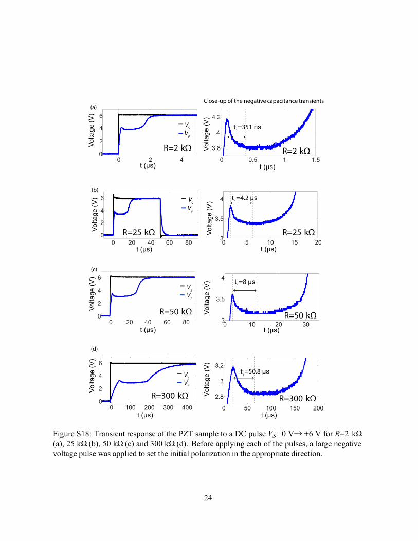
Fig. S18(a,b,c,d) show the transient response of the PZT sample to a DC pulse VS : 0 V→
+6 V for R=2 kΩ, 25 kΩ, 50 kΩ and 300 kΩ respectively. The time duration of the negative
capacitance transient t1 is indicated in the close-up images in Fig. S18(a,b,c,d). Fig. S19(a,b)

19
V :
V
V V
V V
V
V
V Q
(nC
) Q
(n
C)
Q
(nC
) Q
(n
C)
Q
(nC
) F
F F
F F
Q
(nC
) Q
(n
C)
Q
(nC
) Q
(n
C)
Q
(nC
) F
F F
F F
Q
(nC
) Q
(n
C)
Q
(nC
) Q
(n
C)
Q
(nC
) F
F F
F F
(a) 1
0.5
0
−0.5
R=300 kΩ R=50 kΩ V : 0 V->+4 V
(b) 1
0.5
0
−0.5
R=300 kΩ R=50 kΩ
VS
(c) 1
0.5
0
−0.5
V : 0 V->+4 V
−1
0.5
0
−0.5
−1
S
: 0 V->+5 V S
−1
0.5
0 −0.5 −1
: 0 V->+4 V VS 0 V->+5 V
−1
0.5
0 −0.5 −1
S
: 0 V->+5 V S
0.5
0.5
0.5
0
−0.5
−1
VS: 0 V->+5.8 V
0
−0.5 −1
: 0 V->+5.8 V S
0
−0.5 −1
: 0 V->+5.8 V S
0.5
0.5
0.5
0
−0.5
−1
0.5
0
−0.5
−1
: 0 V->+7.6 V S
VS: 0 V->+9.6 V
0
−0.5 −1
0.5
0
−0.5 −1
: 0 V->+7.6 V S
: 0 V->+9.6 V S
0
−0.5 −1
0.5
0
−0.5 −1
: 0 V->+7.6 V S
: 0 V->+9.6 V S
2 3 4 5 6 0 0.5 1 1.5 x 10⁻⁴
0 10 20 100
VF (V ) i
F (A) ρ (kΩ)
Figure S15: (a,b) QF − VF (a) and QF − iF (b) curves for different applied voltage amplitudes with R= 50 kΩ and R= 300 kΩ. (c) The value of ρ calculated using equation 13 as a function of QF for different voltage amplitudes.
plot t1 as a function of R in logarithmic and linear scale respectively. In fig. S19(a,b), we
observe a linear decrease of t1 down to ~∼350 ns as R is decreased to 2 kΩ. Fig. S19(c) shows
that the extrapolated t1 − R curve intersects the R = 0 line at t1=19.9 ns.
20
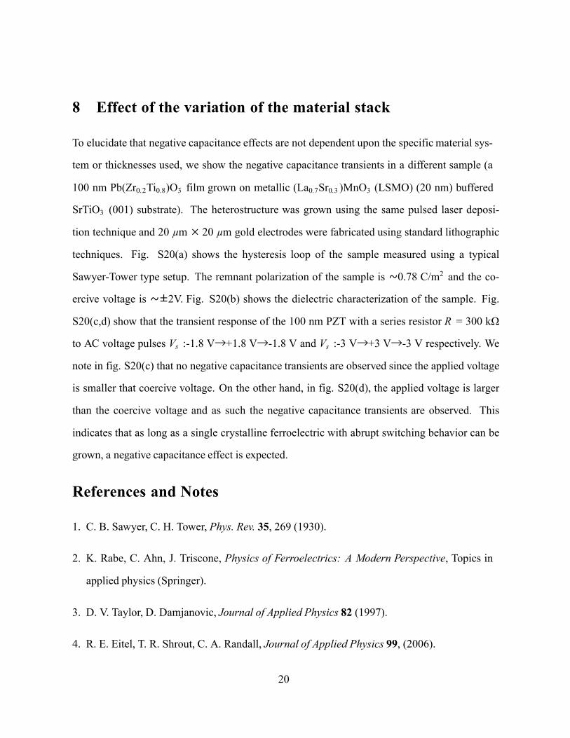
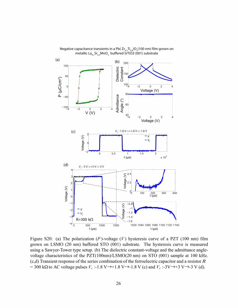
8 Effect of the variation of the material stack To elucidate that negative capacitance effects are not dependent upon the specific material sys-
tem or thicknesses used, we show the negative capacitance transients in a different sample (a
100 nm Pb(Zr0.2 Ti0.8)O3 film grown on metallic (La0.7Sr0.3 )MnO3 (LSMO) (20 nm) buffered
SrTiO3 (001) substrate). The heterostructure was grown using the same pulsed laser deposi-
tion technique and 20 µm × 20 µm gold electrodes were fabricated using standard lithographic
techniques. Fig. S20(a) shows the hysteresis loop of the sample measured using a typical
Sawyer-Tower type setup. The remnant polarization of the sample is ~∼0.78 C/m2 and the co-
ercive voltage is ~∼±2V. Fig. S20(b) shows the dielectric characterization of the sample. Fig.
S20(c,d) show that the transient response of the 100 nm PZT with a series resistor R = 300 kΩ
to AC voltage pulses Vs :-1.8 V→+1.8 V→-1.8 V and Vs :-3 V→+3 V→-3 V respectively. We
note in fig. S20(c) that no negative capacitance transients are observed since the applied voltage
is smaller that coercive voltage. On the other hand, in fig. S20(d), the applied voltage is larger
than the coercive voltage and as such the negative capacitance transients are observed. This
indicates that as long as a single crystalline ferroelectric with abrupt switching behavior can be
grown, a negative capacitance effect is expected.
References and Notes 1. C. B. Sawyer, C. H. Tower, Phys. Rev. 35, 269 (1930).
2. K. Rabe, C. Ahn, J. Triscone, Physics of Ferroelectrics: A Modern Perspective, Topics in
applied physics (Springer).
3. D. V. Taylor, D. Damjanovic, Journal of Applied Physics 82 (1997).
4. R. E. Eitel, T. R. Shrout, C. A. Randall, Journal of Applied Physics 99, (2006).

21
5. C. Pawlaczyk, et al., Integrated Ferroelectrics 9, 293 (1995).
22
ΔQ S
Δ
F S Δ
Δ
ΔQ S
ΔQ
Δ
ΔQ
−
V
Q
(nC
) Q
(n
C)
Q
(nC
) Q
(n
C)
Q
(nC
) F
F F
F F
V
−1
−1
1
0.5
0
−0.5 F
V : 0 V->+4 V
−1 int
0.5
0
−0.5
ΔQ V : 0 V->+5 V
V int
0.5
0
−0.5
−1
F
V int
V : 0 V->+5.8 V
0.5
0
−0.5
F
V : 0 V->+7.6 V
V S int
0.5
0
−0.5
F
V : 0 V->+9.6 V
1 ΔV S
int
2 3 4 5 6
int (V ) Figure S16: QF − Vint curves for different voltage pulses. The negative capacitance state of the ferroelectric corresponds to the region under the dashed box.
23
ρ (kΩ
)
-C
(pF)
FE
(a) 15
10
5
(b) 1000
500
0
0 4 8 12
0
4 6 8 10 Applied Pulse Magnitude (V) Applied Pulse Magnitude (V)
Figure S17: Average ρ (a) and −CF E (b) as functions of the applied voltage magnitude.
24
Volta
ge (V
) Vo
ltage
(V)
Volta
ge (V
) Vo
ltage
(V)
Volta
ge (V
) Vo
ltage
(V)
Volta
ge (V
) Vo
ltage
(V)
V
(a) 6
4
2
Close-up of the negative capacitance transients
4.2 V
S 4
t1=351 ns
F
R=2 kΩ 0
3.8 R=2 kΩ 0 2 4
t (µs) 0 0.5 1 1.5
t (µs)
(b) 6
4
2
0
R=25 kΩ
V 4
S
V F
3.5
3
t 1
=4.2 µs R=25 kΩ
0 20 40 60 80 t (µs)
0 5 10 15 20 t (µs)
(c) 6
4
2
0
V S
V F
R=50 kΩ
4
3.5
3
t
1=8 µs
R=50 kΩ
0 20 40 60 80 t (µs)
0 10 20 30 t (µs)
(d)
6
4
2
0
V S
V F
R=300 kΩ
3.2
3 2.8
t
1=50.8 µs
R=300 kΩ
0 100 200 300 400 0 50 100 150 200 t (µs) t (µs)
Figure S18: Transient response of the PZT sample to a DC pulse VS : 0 V→ +6 V for R=2 kΩ (a), 25 kΩ (b), 50 kΩ (c) and 300 kΩ (d). Before applying each of the pulses, a large negative voltage pulse was applied to set the initial polarization in the appropriate direction.

25
4
1
1
1
1
Tim
e sc
ale
for n
egat
ive
capa
cita
nce
trans
ient
t (
ns)
1
Tim
e sc
ale
for n
egat
ive
capa
cita
nce
trans
ient
t (
ns)
1
Tim
e sc
ale
for n
egat
ive
capa
cita
nce
trans
ient
t (
ns)
1
(a) 106
R=300 kΩ
(b)
6 x 10
R=300 kΩ
105
104
103
102
R=25 kΩ t1=4.2 µs
R=2 kΩ t =351 ns
t1=50.8 µs
R=50 kΩ t1=8 µs
5 R=25 kΩ t =50.8 µs t =4.2 µs
4 1
3
2
1
0
−1
R=50 kΩ t =8 µs
R=2 kΩ t1=351 ns
100 101 102
R (kΩ) 0 200 400
R (kΩ)
(c) 500
400
300
200
100
0
t =19.9 ns
−100 −10 −5 0 5 10
R (kΩ) Figure S19: (a,b) The time duration of the negative capacitance transient t1 as a function of R in logarithmic (a) and linear scale (b). (c) Extrapolation of t1 vs. R curve to R = 0.
26
S
P (µ
C/c
m2 )
Vo
ltage
(V)
Volta
ge (V
)
Adm
ittan
ce
Ang
le (0 )
Die
lect
ric
Con
stan
t Vo
ltage
(V)
Volta
ge (V
)
Negative capacitance transients in a Pb( Zr0.2Ti0.8)O3(100 nm) film grown on metallic La0.7Sr0.3MnO3 buffered SrTiO3 (001) substrate
(a) (b) 100
50
0
200 150 100 −4 −2 0 2 4
Voltage (V)
−50
−100 −4 −2 0 2 4
V (V)
(c) 2
0
90
60
30 −4 −2 0 2 4
Voltage (V) VS: -1.8 V->+1.8 V->-1.8 V
V V F
−2 0 0.5 1 1.5 2
t (µs)
x 104
(d)
4
3
V : -3 V->+3 V->-3 V
2.4
2 2.2
1 2
0 100 200 300 400 0 t (µs)
−1
−2 V V F
−3
−0.8 −1
−1.2 −1.4
R=300 kΩ −4 0 500 1000 1500
−1.6 1020 1040 1060 1080 1100 1120 1140
t (µs) t (µs) Figure S20: (a) The polarization (P )-voltage (V ) hysteresis curve of a PZT (100 nm) film grown on LSMO (20 nm) buffered STO (001) substrate. The hysteresis curve is measured using a Sawyer-Tower type setup. (b) The dielectric constant-voltage and the admittance angle- voltage characteristics of the PZT(100nm)/LSMO(20 nm) on STO (001) sample at 100 kHz. (c,d) Transient response of the series combination of the ferroelectric capacitor and a resistor R = 300 kΩ to AC voltage pulses Vs :-1.8 V→+1.8 V→-1.8 V (c) and Vs :-3V→+3 V→-3 V (d).