Embed Size (px)
Citation preview
IOP PUBLISHING NANOTECHNOLOGY
Nanotechnology 20 (2009) 115301 (7pp) doi:10.1088/0957-4484/20/11/115301
Nanoscale ripples on polymers created bya focused ion beamMyoung-Woon Moon1, Jun Hyun Han2, Ashkan Vaziri3,6,Eun Kyu Her4, Kyu Hwan Oh4, Kwang-Ryeol Lee1 andJohn W Hutchinson5,6
1 Future Fusion Technology Laboratory, Korea Institute of Science and Technology,Seoul 136-791, Republic of Korea2 Materials Science and Technology Research Division, Korea Institute of Science andTechnology, Seoul 136-791, Republic of Korea3 Department of Mechanical and Industrial Engineering, Northeastern University, Boston,MA 02115, USA4 Department of Materials Science and Engineering, Seoul National University,Seoul 151-744, Republic of Korea5 School of Engineering and Applied Sciences, Harvard University, Cambridge,MA 02138, USA
E-mail: [email protected] and [email protected]
Received 10 December 2008, in final form 12 January 2009Published 24 February 2009Online at stacks.iop.org/Nano/20/115301
AbstractWe show that focused ion beam irradiation results in the creation of peculiar one- andtwo-dimensional nanoscale features on the surface of polyimide—a common polymer inelectronics, large scale structures, and the automobile industry, as well as in biomedicalapplications. The role of ion beam incident angle, acceleration voltage, and fluence on themorphology of the structural features is systematically investigated, and insights into themechanisms of formation of these nanoscale features are provided. Moreover, by using themaskless patterning method of the focused ion beam system, we have developed a robusttechnique for controlled modification of the polymeric surface. The technique, which isanalogous to using a gray glass with varying darkness to control the radiation from the sun, butat a much smaller scale, enables the ion intensity and angle to be controlled at each surface pointof the polymer, giving rise to structural surface features with desired shape and morphology.
M This article features online multimedia enhancements
(Some figures in this article are in colour only in the electronic version)
1. Introduction
Ion beam irradiation has been used extensively for surfacemodification of polymers, glassy metals, and amorphous andcrystalline materials at micron and submicron scales [1–6].The surface structures created by exposure to an ion beamrange from dots, steps, and one-dimensional (1D) straightwrinkles to highly complex hierarchical undulations andripples [5–13]. In general, the morphology of these nanoscalefeatures can be selected by controlling the ion beam parameters(e.g. fluence and acceleration voltage), making ion beam
6 Authors to whom any correspondence should be addressed.
irradiation a promising method for the surface engineeringof materials. An example is the recent experiments onpolydimethalsiloxane (PDMS) [13–15], which have providednew avenues for controlled surface modification. Theirradiation of a Ga+ focused ion beam (FIB) on the surface ofa compliant polymer results in the formation of a wrinkled stiffskin on the polymer, with overall morphology and wavelengththat can be controlled by selecting the ion beam parameters.The capabilities of this technique have been recently extendedby using maskless patterning of the focused ion beamsystem [13–15]. This yields a robust technique for controlledsurface modification that can be used for a wide range of
0957-4484/09/115301+07$30.00 © 2009 IOP Publishing Ltd Printed in the UK1
Nanotechnology 20 (2009) 115301 M-W Moon et al
interdisciplinary applications including microfluidics, flexibleelectronics, biosensors, tissue engineering, and regenerativemedicine [16–18].
In this paper, we examine for the first time the effect offocused ion beam irradiation on a polyimide (PI) substrate—amuch stiffer polymer than PDMS, with an elastic modulus of1–10 GPa (compared to ∼1 MPa for PDMS [19]). Polyimide,due to its unique properties (e.g. high strength, and heatand chemical resistance) as well as its excellent biostabilityand biocompatibility properties, has become a very commonpolymer in electronics, large scale structures, and the carindustry, as well as in biomedical applications [20–25]. Weshow that ion beam irradiation leads to the formation of rippleson the PI surface, with morphology and direction that canbe controlled by the ion beam parameters. We provide someinsights into the mechanisms of formation of these peculiarstructural features by examining the chemical compositions ofthe polymer surface after irradiation.
In a second set of experiments, we have developed arobust technique for the creation of structural features onselected small surfaces of the polymer using the masklesspatterning method of a focused ion beam system. Examplesof the peculiar three-dimensional (3D) features created onthe PI surface using the technique are provided. The keyadvantages and some of the potential applications of theproposed technique are also highlighted briefly.
2. Experimental details
Polyimide (UPILEX-25S, JAPAN) coupons of size 20 mm ×20 mm × 0.1 mm were used in our experiment with anelastic modulus ∼ 9 GPa and density 1.47 g cm−3 (at roomtemperature). A field emission (FE)-SEM/FIB dual beamsystem (FE-SEM/FIB Dual Beam NOVA; FEI, Hillsboro, OR)was used for focused ion beam irradiation. The polyimidecoupons were placed in the high vacuum chamber under aworking pressure of ≈10−5 Pa. Prior to ion beam exposure,a 3 nm Au layer was deposited on the polyimide substrate toprevent the polymer surface from electron-charging.
The acceleration voltage and ion current were variedover the ranges 10–30 keV and 1–20 nA, respectively. Theirradiation angle, defined as the angle between the incomingbeam and the surface normal, was varied between 0◦ and∼90◦. The beam dwell time was kept at 3 μs in all theexperiments. The images in the exposed region were takenwith a built-in secondary electron microscope (SEM) in the FE-SEM/FIB system. The morphology of the surface structureswas examined using an atomic force microscope (AFM;Nanoscope III, Digital Instrument, NY) in the tapping modeat ambient conditions. In each experiment, the morphology ofthe surface patterns was typically measured on five differentsurface regions of the polymer.
The cross-sectional microstructure (prepared with theFE-SEM/FIB system) of the polymeric substrate near itssurfaces was explored with a high-resolution transmissionelectron microscope (TEM; JEM-3000F, JEOL). Moreover,the chemical composition of the surface layer through thedepth was analyzed using energy dispersive x-ray spectroscopy
(EDS, OXFORD). Electron energy loss spectroscopy (EELS),in conjunction with a high voltage electron microscope(HVEM, JEOL), was also employed to examine thecompositional change of the surface layer on the PI surfaceinduced by FIB irradiation.
The maskless patterning method of the FIB equipmentwas adopted for the creation of 3D morphologies guided bypredefined bitmap images. This method permits the accurateselection of the areas exposed to the FIB. Bitmap files of theexposure patterns were imported as a virtual mask in the FIBsystem. Then, the surface area of the PI substrate (20 μm ×20 μm) was subjected to the FIB irradiation.
3. Results and discussion
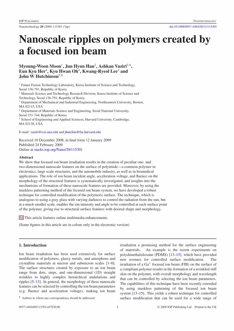
Figure 1(A) shows the schematics of the experiment, in which a10 μm × 10 μm surface area of the PI substrate was subjectedto the ion beam at a constant incident angle and accelerationvoltage. When the incident angle is normal to the surface,the exposure of the surface to the ion beam results in millingof the substrate with no surface undulation and instability. Asimilar set of experiments was performed on a Si substrate,leading to a similar outcome. The dependence of the millingdepth on the fluence and acceleration voltage of the ion beamis quantified for both PI and the Si substrate in figure 1(B).Here, the milling depth was measured by the SEM as theexposure time increased from 30 to 600 s (corresponding toan ion fluence of 4.6 × 10¹⁶ to 47 × 1016 ions cm−2) at twoion acceleration voltages. Interestingly, the milling rate is verysimilar for both PI and the Si substrate. Figures 1(C) showsthe patterns created by the FIB irradiation on the PI surface atincident angles of 45◦ and 85◦, and the evolution of the patternsas the exposure time and, therefore, ion fluence, increases.The ion beam irradiation leads to the creation of nanoscalestructural features on the polymeric surface, which manifestthemselves as nanoscale ripple morphologies. For the ionincident angle 45◦, the ripple vector was first created parallelto the projected ion beam (black arrow). With increasingexposure time, the amplitude of the ripples increases, while thewavelength of the ripples is almost constant, at 320 nm. For anion beam incident angle 85◦, the ripple structures appear as 1Dundulations but normal to the projected ion beam. Now withincreased exposure time, the 1D ripple morphology evolvesto complex 1D columnar patterns, while the amplitude ofthe patterns increases rapidly. The wavelength of the ripplesincreases slightly with the exposure duration from ∼300 to∼500 nm for 30 keV. The acceleration voltage and current ofthe ion beam in this set of experiments were 30 keV and 7 nA,respectively. The dependence of the amplitude and wavelengthof the morphologies will be taken up again in what follows.
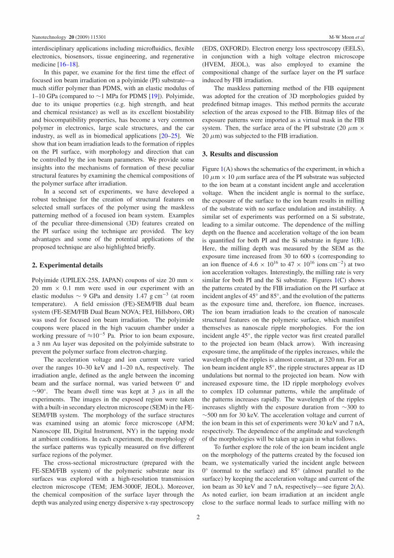
To further explore the role of the ion beam incident angleon the morphology of the patterns created by the focused ionbeam, we systematically varied the incident angle between0◦ (normal to the surface) and 85◦ (almost parallel to thesurface) by keeping the acceleration voltage and current of theion beam as 30 keV and 7 nA, respectively—see figure 2(A).As noted earlier, ion beam irradiation at an incident angleclose to the surface normal leads to surface milling with no
2
Nanotechnology 20 (2009) 115301 M-W Moon et al
Figure 1. Creation of ripples on the surface of polyimide by a focused ion beam. (A) Schematic of the experiment. (B) Milling depth versusion fluence for both PI and SI substrate subject to focused ion beam irradiation with incident angle 0◦ at two acceleration voltages, 10 and30 keV. (C) Evolution of the polyimide surface by exposure to ion beam at the incident angle (projection direction of ion beam, u) of 45◦ (leftpanels) and 85◦ (right panels). The acceleration voltage and ion current were 30 keV and 7 nA, respectively, for this set of experiments. Scalebar = 5 μm.
surface undulation and instability—as quantified in figure 1(B).With increasing incident angle, ripple morphologies appear ata critical angle of approximately 30◦ for this set of ion beamparameters. This is confirmed by examining the surface usingan atomic force microscope in the tapping mode at ambientconditions. The ripple patterns on the polymeric surfacecreated at the incident angle 30◦ have the wavevector alignedalong the ion beam projected direction. With further increasein the incident angle, the formation of two-dimensional (2D)columnar structures sets in, at the incident angle ∼55◦. Thiscritical incident angle is found not to be very sensitive to the
ion accelerating voltage in the range studied here (5–30 keV).A further increase in the incident angle (>80◦, where the ionbeam is approximately parallel to the polymer surface) leadsto the formation of 1D ripple morphologies but normal to thedirection of irradiation. The underlying mechanisms producingthese peculiar morphologies and their transitions tied to theincident beam angle are not understood. It is noteworthythat the peculiar transition in surface structure with changein the incident angle has been also observed in experimentson aluminum thin films [26] and Si/amorphous Si [8, 9]. Itwas suggested that once a ripple pattern forms by ion beam
3
Nanotechnology 20 (2009) 115301 M-W Moon et al
Figure 2. Ordered structural features created at different ion beam incident angles (θ). (A) The panels show the morphology of the patternscreated on the surface of originally flat polyimide substrate by 3 min exposure to the focused ion beam along the projection direction u. Theacceleration voltage and current density of the ion beam were 30 keV and 7 nA, respectively. Scale bar = 5 μm. (B) Amplitude andwavelength of ripple structures created by focused ion beam irradiation with incident angle 50◦, versus the exposure time. The accelerationvoltage and current density of the ion beam were 30 keV and 7 nA, respectively. (C) Role of ion beam incident angle on the wavelength ofcreated ordered structures for three acceleration voltages (5, 10, and 30 keV) at 5 min exposure time. The current density of the ion beam was7 nA.
irradiation, the erosion rate at the valley regions (concaveregion) of ripple patterns can be higher than that at the convexregion [1], which could lead to this transition from the step-like structure into 1D-like surface structures with increase ofion fluence or exposure time.
Figures 2(B) and (C) show the role of ion beam parameterson the morphology of the patterns. The wavelength andamplitude of patterns created at different acceleration voltage,incident angle, and ion fluence were measured using an AFM.The wavelength of the patterns is mainly controlled by theion beam acceleration voltage, while the amplitude is mainlydependent on the fluence or, equivalently, on the irradiationtime (see figure 2(B) for a set of results measured at theion incident angle 50◦ and acceleration voltage 30 keV). Thewavelength increases only slightly with the exposure time (inthe range 300–500 nm), while the amplitude is much moresensitive to this parameter. Figure 2(C) shows the dependence
of the wavelength and amplitude of the structural features onthe ion beam incident angle for three acceleration voltages: 5,10, and 30 keV. The wavelengths of the patterns increased from∼55 to ∼370 nm, while slightly depending on the incidentangle.
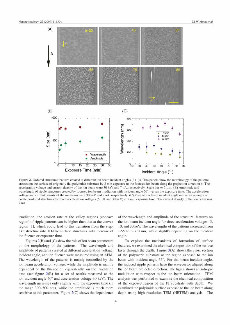
To explore the mechanisms of formation of surfacefeatures, we examined the chemical composition of the surfacelayer through the depth. Figure 3(A) shows the cross sectionof the polymeric substrate at the region exposed to the ionbeam with incident angle 55◦. For this beam incident angle,the induced ripple patterns have the wavevector aligned alongthe ion beam projected direction. The figure shows anisotropicundulation with respect to the ion beam orientation. TEManalysis was performed to examine the chemical compositionof the exposed region of the PI substrate with depth. Weexamined the polyimide surface exposed to the ion beam alongdepth using high resolution TEM (HRTEM) analysis. The
4
Nanotechnology 20 (2009) 115301 M-W Moon et al
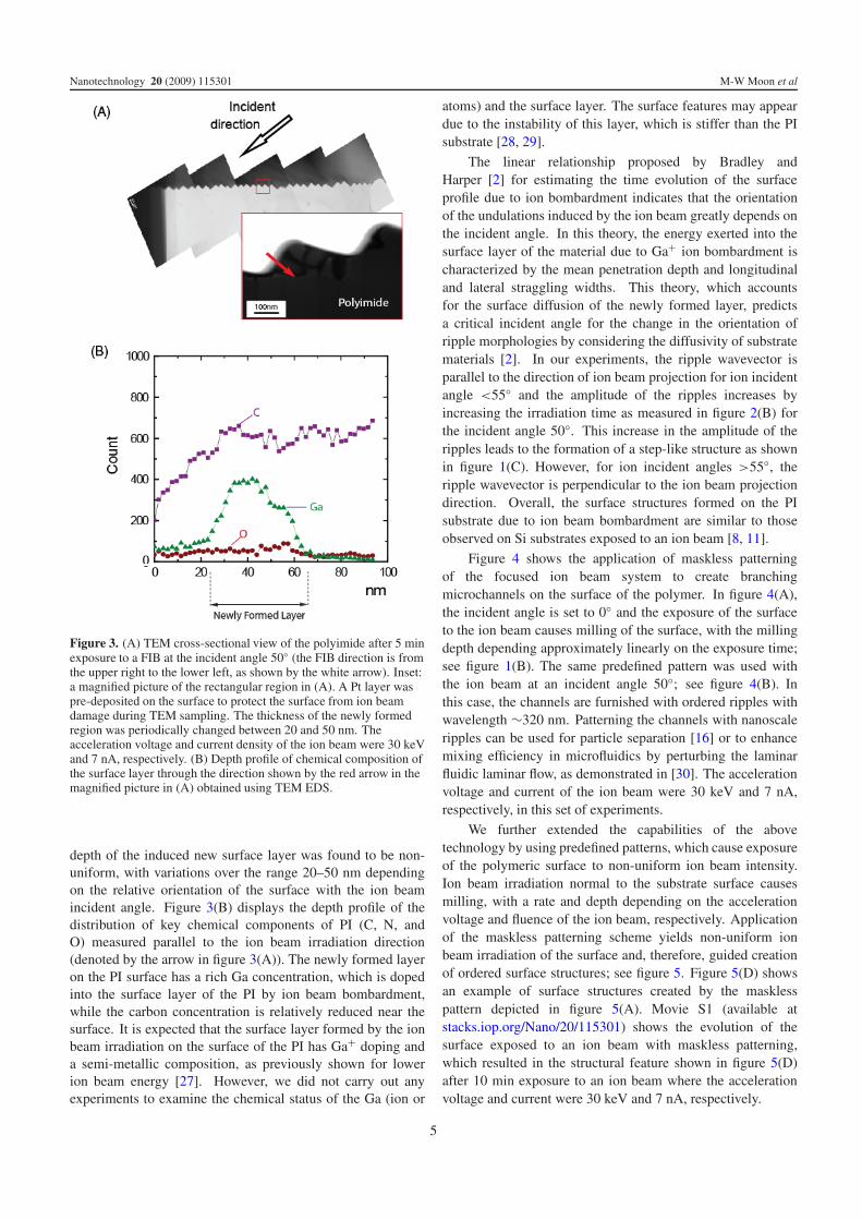
Figure 3. (A) TEM cross-sectional view of the polyimide after 5 minexposure to a FIB at the incident angle 50◦ (the FIB direction is fromthe upper right to the lower left, as shown by the white arrow). Inset:a magnified picture of the rectangular region in (A). A Pt layer waspre-deposited on the surface to protect the surface from ion beamdamage during TEM sampling. The thickness of the newly formedregion was periodically changed between 20 and 50 nm. Theacceleration voltage and current density of the ion beam were 30 keVand 7 nA, respectively. (B) Depth profile of chemical composition ofthe surface layer through the direction shown by the red arrow in themagnified picture in (A) obtained using TEM EDS.
depth of the induced new surface layer was found to be non-uniform, with variations over the range 20–50 nm dependingon the relative orientation of the surface with the ion beamincident angle. Figure 3(B) displays the depth profile of thedistribution of key chemical components of PI (C, N, andO) measured parallel to the ion beam irradiation direction(denoted by the arrow in figure 3(A)). The newly formed layeron the PI surface has a rich Ga concentration, which is dopedinto the surface layer of the PI by ion beam bombardment,while the carbon concentration is relatively reduced near thesurface. It is expected that the surface layer formed by the ionbeam irradiation on the surface of the PI has Ga+ doping anda semi-metallic composition, as previously shown for lowerion beam energy [27]. However, we did not carry out anyexperiments to examine the chemical status of the Ga (ion or
atoms) and the surface layer. The surface features may appeardue to the instability of this layer, which is stiffer than the PIsubstrate [28, 29].
The linear relationship proposed by Bradley andHarper [2] for estimating the time evolution of the surfaceprofile due to ion bombardment indicates that the orientationof the undulations induced by the ion beam greatly depends onthe incident angle. In this theory, the energy exerted into thesurface layer of the material due to Ga+ ion bombardment ischaracterized by the mean penetration depth and longitudinaland lateral straggling widths. This theory, which accountsfor the surface diffusion of the newly formed layer, predictsa critical incident angle for the change in the orientation ofripple morphologies by considering the diffusivity of substratematerials [2]. In our experiments, the ripple wavevector isparallel to the direction of ion beam projection for ion incidentangle <55◦ and the amplitude of the ripples increases byincreasing the irradiation time as measured in figure 2(B) forthe incident angle 50◦. This increase in the amplitude of theripples leads to the formation of a step-like structure as shownin figure 1(C). However, for ion incident angles >55◦, theripple wavevector is perpendicular to the ion beam projectiondirection. Overall, the surface structures formed on the PIsubstrate due to ion beam bombardment are similar to thoseobserved on Si substrates exposed to an ion beam [8, 11].
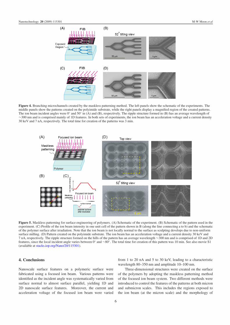
Figure 4 shows the application of maskless patterningof the focused ion beam system to create branchingmicrochannels on the surface of the polymer. In figure 4(A),the incident angle is set to 0◦ and the exposure of the surfaceto the ion beam causes milling of the surface, with the millingdepth depending approximately linearly on the exposure time;see figure 1(B). The same predefined pattern was used withthe ion beam at an incident angle 50◦; see figure 4(B). Inthis case, the channels are furnished with ordered ripples withwavelength ∼320 nm. Patterning the channels with nanoscaleripples can be used for particle separation [16] or to enhancemixing efficiency in microfluidics by perturbing the laminarfluidic laminar flow, as demonstrated in [30]. The accelerationvoltage and current of the ion beam were 30 keV and 7 nA,respectively, in this set of experiments.
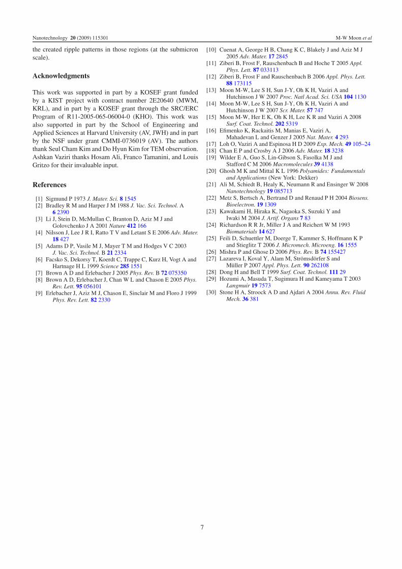
We further extended the capabilities of the abovetechnology by using predefined patterns, which cause exposureof the polymeric surface to non-uniform ion beam intensity.Ion beam irradiation normal to the substrate surface causesmilling, with a rate and depth depending on the accelerationvoltage and fluence of the ion beam, respectively. Applicationof the maskless patterning scheme yields non-uniform ionbeam irradiation of the surface and, therefore, guided creationof ordered surface structures; see figure 5. Figure 5(D) showsan example of surface structures created by the masklesspattern depicted in figure 5(A). Movie S1 (available atstacks.iop.org/Nano/20/115301) shows the evolution of thesurface exposed to an ion beam with maskless patterning,which resulted in the structural feature shown in figure 5(D)after 10 min exposure to an ion beam where the accelerationvoltage and current were 30 keV and 7 nA, respectively.
5
Nanotechnology 20 (2009) 115301 M-W Moon et al
Figure 4. Branching microchannels created by the maskless patterning method. The left panels show the schematic of the experiments. Themiddle panels show the patterns created on the polyimide substrate, while the right panels display a magnified region of the created patterns.The ion beam incident angles were 0◦ and 50◦ in (A) and (B), respectively. The ripple structure formed in (B) has an average wavelength of∼300 nm and is comprised mainly of 1D features. In both sets of experiments, the ion beam has an acceleration voltage and a current density30 keV and 7 nA, respectively. The total time for creation of the patterns was 3 min.
Figure 5. Maskless patterning for surface engineering of polymers. (A) Schematic of the experiment. (B) Schematic of the pattern used in theexperiment. (C) Profile of the ion beam intensity in one unit cell of the pattern shown in B (along the line connecting a to b) and the schematicof the polymer surface after irradiation. Note that the ion beam is not locally normal to the surface as sculpting develops due to non-uniformsurface milling. (D) Pattern created on the polyimide substrate. The ion beam has an acceleration voltage and a current density 30 keV and7 nA, respectively. The ripple structure formed on the hills of the pattern has an average wavelength ∼300 nm and is comprised of 1D and 2Dfeatures, since the local incident angle varies between 0◦ and ∼80◦. The total time for creation of this pattern was 10 min. See also movie S1(available at stacks.iop.org/Nano/20/115301).
4. Conclusions
Nanoscale surface features on a polymeric surface werefabricated using a focused ion beam. Various patterns wereidentified as the incident angle was systematically varied fromsurface normal to almost surface parallel, yielding 1D and2D nanoscale surface features. Moreover, the current andacceleration voltage of the focused ion beam were varied
from 1 to 20 nA and 5 to 30 keV, leading to a characteristicwavelength 80–350 nm and amplitude 10–100 nm.
Three-dimensional structures were created on the surfaceof the polymers by adopting the maskless patterning methodof the focused ion beam system. Two different methods wereintroduced to control the features of the patterns at both micronand submicron scales. This includes the regions exposed tothe ion beam (at the micron scale) and the morphology of
6
Nanotechnology 20 (2009) 115301 M-W Moon et al
the created ripple patterns in those regions (at the submicronscale).
Acknowledgments
This work was supported in part by a KOSEF grant fundedby a KIST project with contract number 2E20640 (MWM,KRL), and in part by a KOSEF grant through the SRC/ERCProgram of R11-2005-065-06004-0 (KHO). This work wasalso supported in part by the School of Engineering andApplied Sciences at Harvard University (AV, JWH) and in partby the NSF under grant CMMI-0736019 (AV). The authorsthank Seul Cham Kim and Do Hyun Kim for TEM observation.Ashkan Vaziri thanks Hosam Ali, Franco Tamanini, and LouisGritzo for their invaluable input.
References
[1] Sigmund P 1973 J. Mater. Sci. 8 1545[2] Bradley R M and Harper J M 1988 J. Vac. Sci. Technol. A
6 2390[3] Li J, Stein D, McMullan C, Branton D, Aziz M J and
Golovchenko J A 2001 Nature 412 166[4] Nilsson J, Lee J R I, Ratto T V and Letant S E 2006 Adv. Mater.
18 427[5] Adams D P, Vasile M J, Mayer T M and Hodges V C 2003
J. Vac. Sci. Technol. B 21 2334[6] Facsko S, Dekorsy T, Koerdt C, Trappe C, Kurz H, Vogt A and
Hartnage H L 1999 Science 285 1551[7] Brown A D and Erlebacher J 2005 Phys. Rev. B 72 075350[8] Brown A D, Erlebacher J, Chan W L and Chason E 2005 Phys.
Rev. Lett. 95 056101[9] Erlebacher J, Aziz M J, Chason E, Sinclair M and Floro J 1999
Phys. Rev. Lett. 82 2330
[10] Cuenat A, George H B, Chang K C, Blakely J and Aziz M J2005 Adv. Mater. 17 2845
[11] Ziberi B, Frost F, Rauschenbach B and Hoche T 2005 Appl.Phys. Lett. 87 033113
[12] Ziberi B, Frost F and Rauschenbach B 2006 Appl. Phys. Lett.88 173115
[13] Moon M-W, Lee S H, Sun J-Y, Oh K H, Vaziri A andHutchinson J W 2007 Proc. Natl Acad. Sci. USA 104 1130
[14] Moon M-W, Lee S H, Sun J-Y, Oh K H, Vaziri A andHutchinson J W 2007 Scr. Mater. 57 747
[15] Moon M-W, Her E K, Oh K H, Lee K R and Vaziri A 2008Surf. Coat. Technol. 202 5319
[16] Efimenko K, Rackaitis M, Manias E, Vaziri A,Mahadevan L and Genzer J 2005 Nat. Mater. 4 293
[17] Loh O, Vaziri A and Espinosa H D 2009 Exp. Mech. 49 105–24[18] Chan E P and Crosby A J 2006 Adv. Mater. 18 3238[19] Wilder E A, Guo S, Lin-Gibson S, Fasolka M J and
Stafford C M 2006 Macromolecules 39 4138[20] Ghosh M K and Mittal K L 1996 Polyamides: Fundamentals
and Applications (New York: Dekker)[21] Ali M, Schiedt B, Healy K, Neumann R and Ensinger W 2008
Nanotechnology 19 085713[22] Metz S, Bertsch A, Bertrand D and Renaud P H 2004 Biosens.
Bioelectron. 19 1309[23] Kawakami H, Hiraka K, Nagaoka S, Suzuki Y and
Iwaki M 2004 J. Artif. Organs 7 83[24] Richardson R R Jr, Miller J A and Reichert W M 1993
Biomaterials 14 627[25] Feili D, Schuettler M, Doerge T, Kammer S, Hoffmann K P
and Stieglitz T 2006 J. Micromech. Microeng. 16 1555[26] Mishra P and Ghose D 2006 Phys. Rev. B 74 155427[27] Lazareva I, Koval Y, Alam M, Stromsdorfer S and
Muller P 2007 Appl. Phys. Lett. 90 262108[28] Dong H and Bell T 1999 Surf. Coat. Technol. 111 29[29] Hozumi A, Masuda T, Sugimura H and Kameyama T 2003
Langmuir 19 7573[30] Stone H A, Stroock A D and Ajdari A 2004 Annu. Rev. Fluid
Mech. 36 381
7