Embed Size (px)
Citation preview
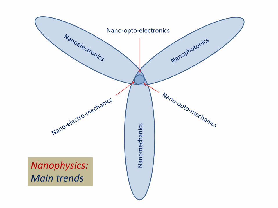
Nan
omec
hani
cs
Nano-opto-electronics
Nanophysics: Main trends
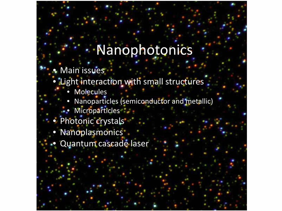
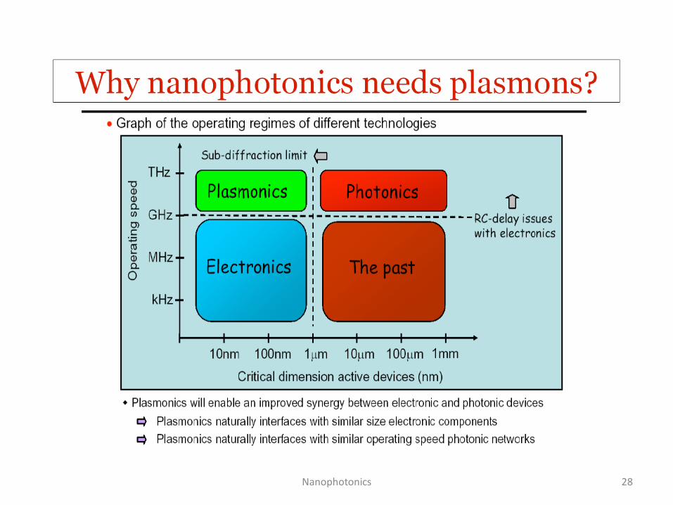
Nanophotonics • Main issues • Light interaction with small structures
• Molecules • Nanoparticles (semiconductor and metallic) • Microparticles
• Photonic crystals • Nanoplasmonics • Quantum cascade laser
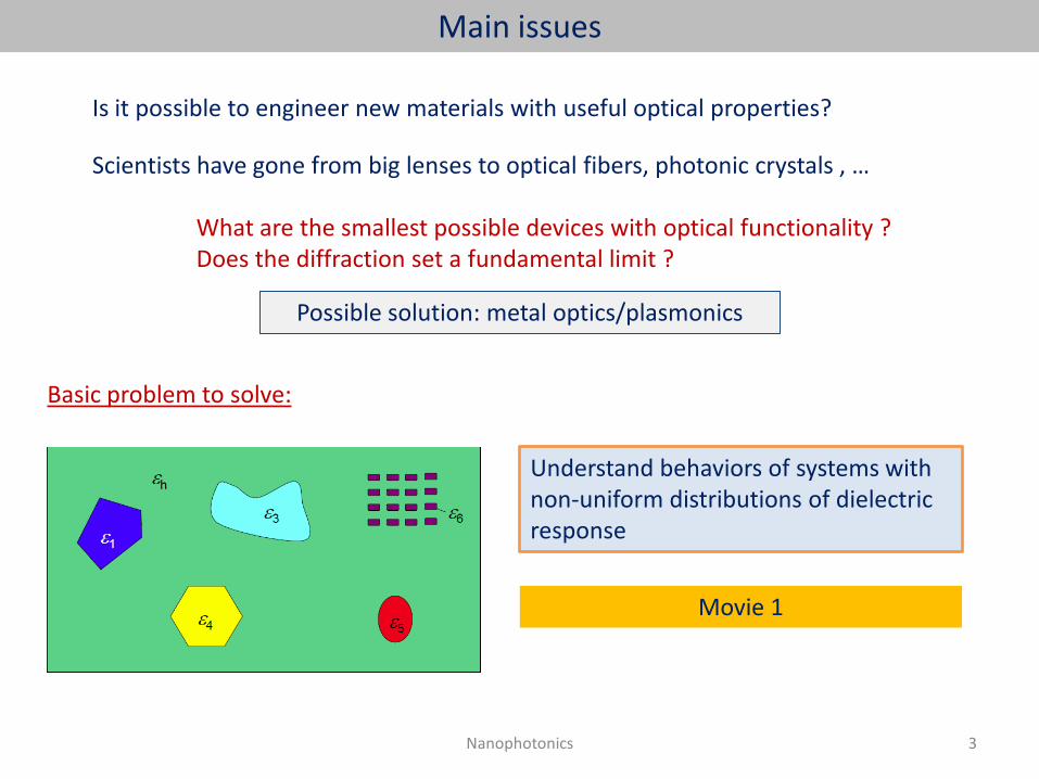
Is it possible to engineer new materials with useful optical properties?
Scientists have gone from big lenses to optical fibers, photonic crystals , … What are the smallest possible devices with optical functionality ? Does the diffraction set a fundamental limit ?
Possible solution: metal optics/plasmonics
Main issues
Basic problem to solve:
Understand behaviors of systems with non-uniform distributions of dielectric response
3 Nanophotonics
Movie 1
Light interaction with small structures
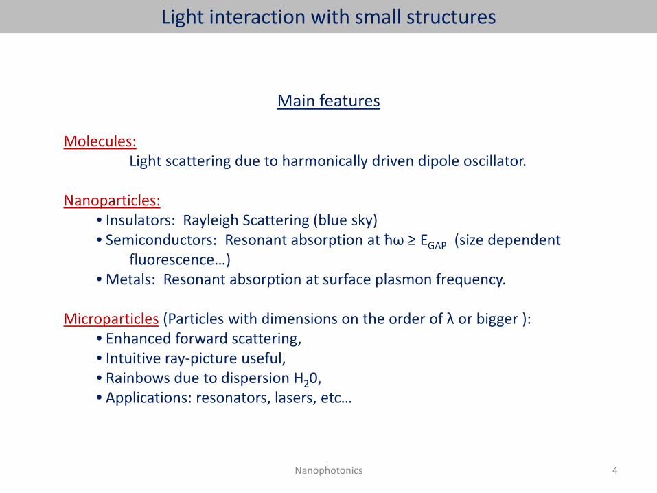
Main features Molecules: Light scattering due to harmonically driven dipole oscillator. Nanoparticles:
• Insulators: Rayleigh Scattering (blue sky) • Semiconductors: Resonant absorption at ħω ≥ EGAP (size dependent fluorescence…) • Metals: Resonant absorption at surface plasmon frequency.
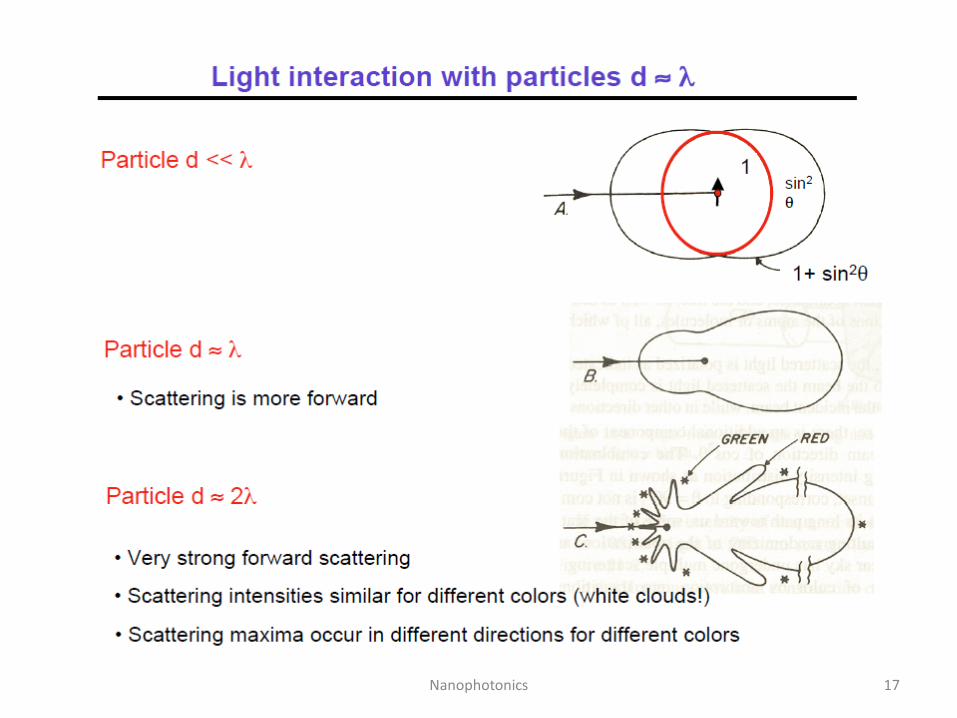
Microparticles (Particles with dimensions on the order of λ or bigger ): • Enhanced forward scattering, • Intuitive ray-picture useful, • Rainbows due to dispersion H20, • Applications: resonators, lasers, etc…
4 Nanophotonics
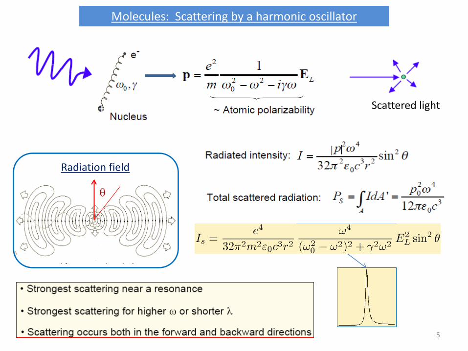
Scattered light
Molecules: Scattering by a harmonic oscillator
5 Nanophotonics
Radiation field
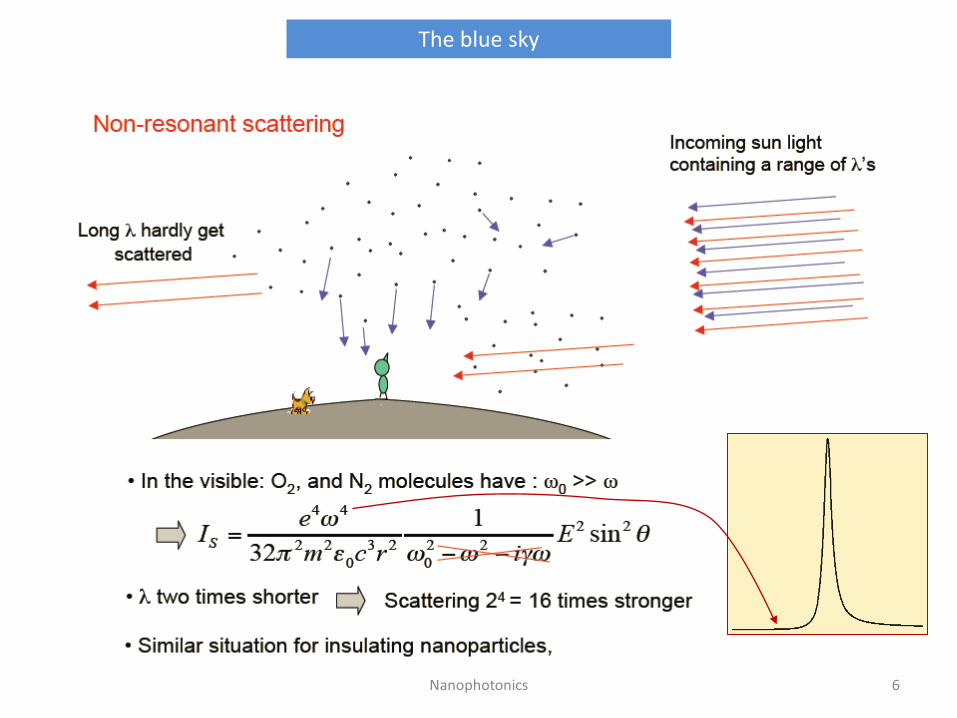
The blue sky
6 Nanophotonics
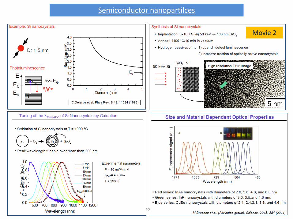
Semiconductor nanopartilces
7 Nanophotonics
Movie 2
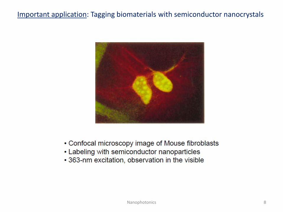
Important application: Tagging biomaterials with semiconductor nanocrystals
8 Nanophotonics
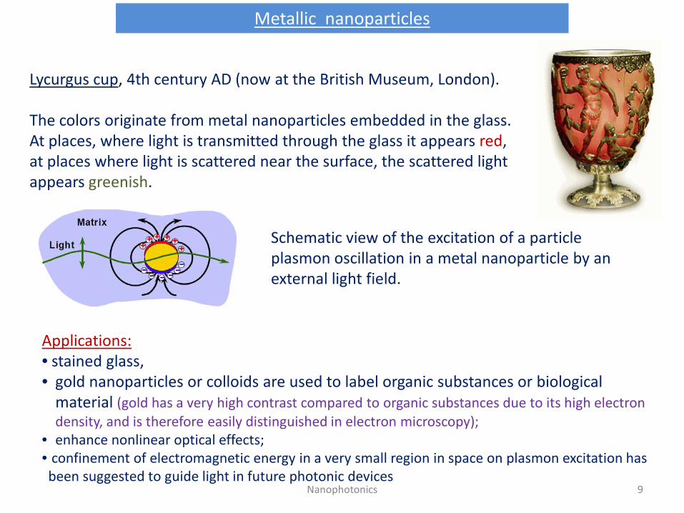
Metallic nanoparticles
Lycurgus cup, 4th century AD (now at the British Museum, London). The colors originate from metal nanoparticles embedded in the glass. At places, where light is transmitted through the glass it appears red, at places where light is scattered near the surface, the scattered light appears greenish.
Schematic view of the excitation of a particle plasmon oscillation in a metal nanoparticle by an external light field.
Applications: • stained glass, • gold nanoparticles or colloids are used to label organic substances or biological
material (gold has a very high contrast compared to organic substances due to its high electron density, and is therefore easily distinguished in electron microscopy);
• enhance nonlinear optical effects; • confinement of electromagnetic energy in a very small region in space on plasmon excitation has been suggested to guide light in future photonic devices
9 Nanophotonics
Nanophotonics 10
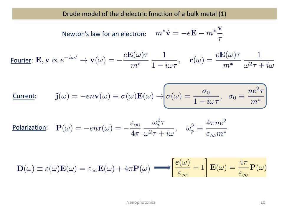
Drude model of the dielectric function of a bulk metal (1)
Newton’s law for an electron:
Fourier:
Current:
Polarization:
Nanophotonics 11
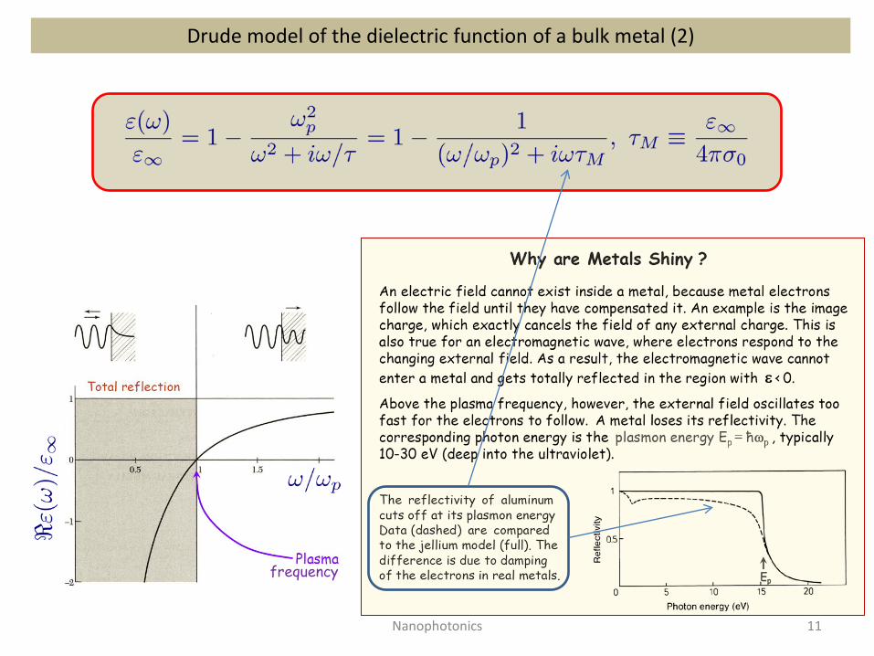
Drude model of the dielectric function of a bulk metal (2)
frequency
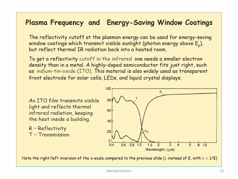
Nanophotonics 12
Nanophotonics 13
Nanophotonics 14
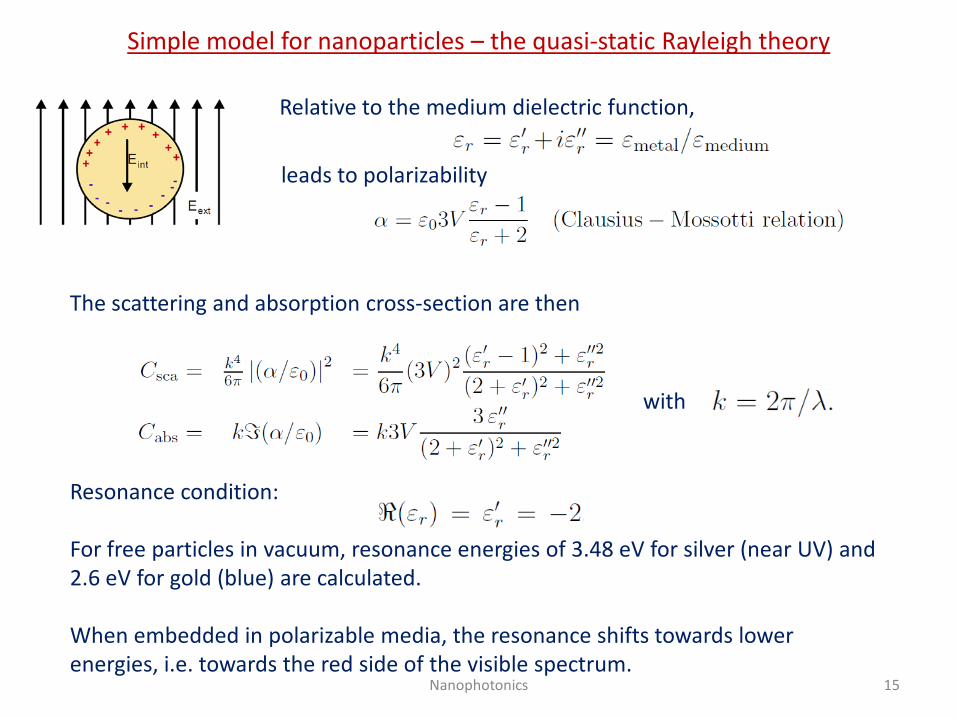
Simple model for nanoparticles – the quasi-static Rayleigh theory
Relative to the medium dielectric function,
leads to polarizability
The scattering and absorption cross-section are then
with
Resonance condition: For free particles in vacuum, resonance energies of 3.48 eV for silver (near UV) and 2.6 eV for gold (blue) are calculated. When embedded in polarizable media, the resonance shifts towards lower energies, i.e. towards the red side of the visible spectrum.
15 Nanophotonics
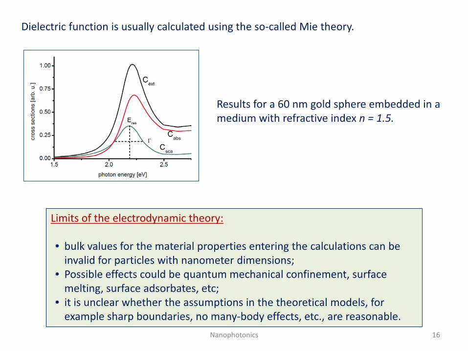
Dielectric function is usually calculated using the so-called Mie theory.
Results for a 60 nm gold sphere embedded in a medium with refractive index n = 1.5.
Limits of the electrodynamic theory: • bulk values for the material properties entering the calculations can be
invalid for particles with nanometer dimensions; • Possible effects could be quantum mechanical confinement, surface
melting, surface adsorbates, etc; • it is unclear whether the assumptions in the theoretical models, for
example sharp boundaries, no many-body effects, etc., are reasonable. 16 Nanophotonics
17 Nanophotonics
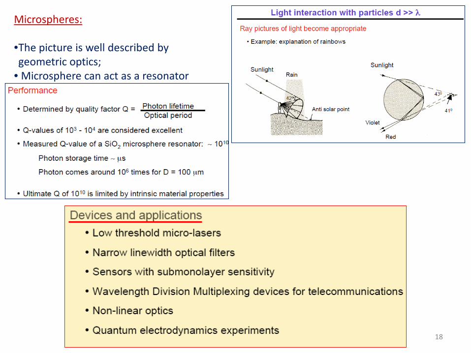
Microspheres: •The picture is well described by geometric optics;
• Microsphere can act as a resonator
18 Nanophotonics
Nanophotonics 19
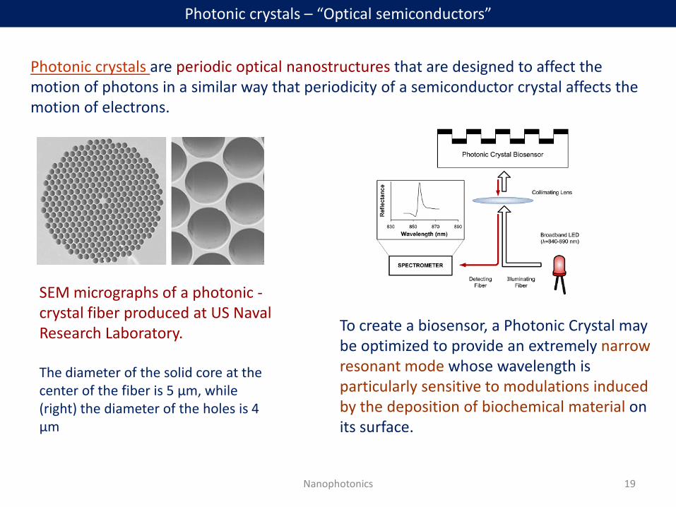
Photonic crystals – “Optical semiconductors”
Photonic crystals are periodic optical nanostructures that are designed to affect the motion of photons in a similar way that periodicity of a semiconductor crystal affects the motion of electrons.
SEM micrographs of a photonic -crystal fiber produced at US Naval Research Laboratory. The diameter of the solid core at the center of the fiber is 5 µm, while (right) the diameter of the holes is 4 µm
To create a biosensor, a Photonic Crystal may be optimized to provide an extremely narrow resonant mode whose wavelength is particularly sensitive to modulations induced by the deposition of biochemical material on its surface.
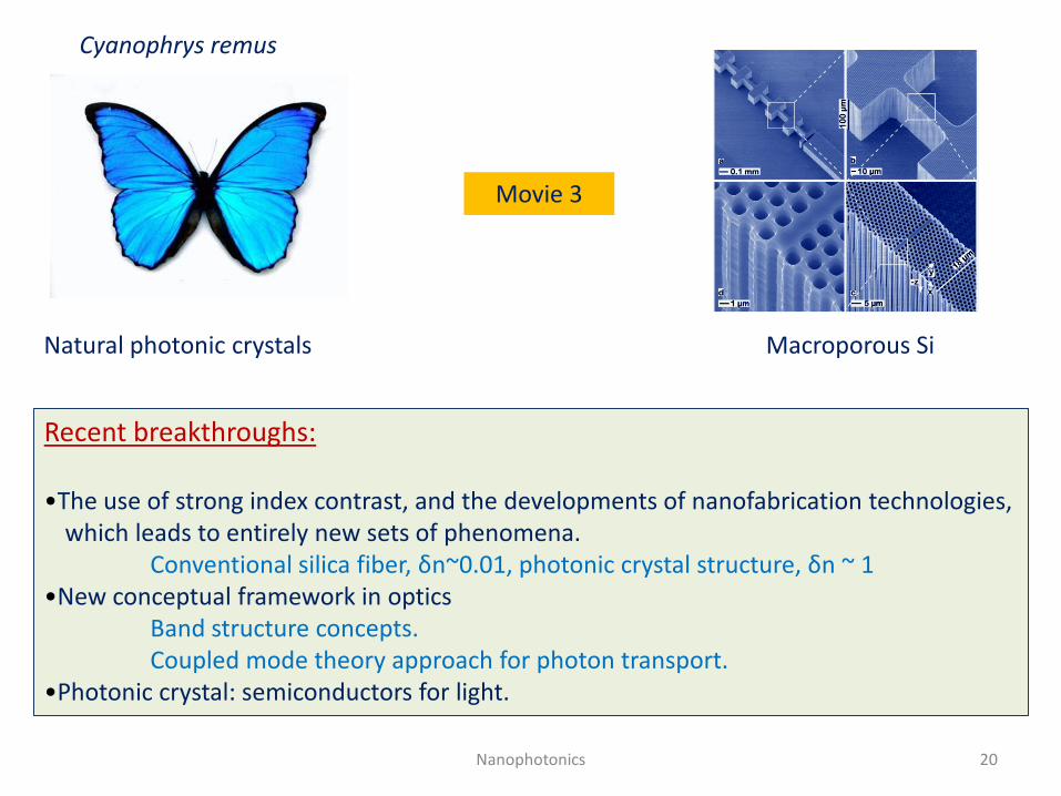
Natural photonic crystals
Cyanophrys remus
Macroporous Si
Recent breakthroughs: •The use of strong index contrast, and the developments of nanofabrication technologies,
which leads to entirely new sets of phenomena. Conventional silica fiber, δn~0.01, photonic crystal structure, δn ~ 1 •New conceptual framework in optics
Band structure concepts. Coupled mode theory approach for photon transport.
•Photonic crystal: semiconductors for light.
20 Nanophotonics
Movie 3
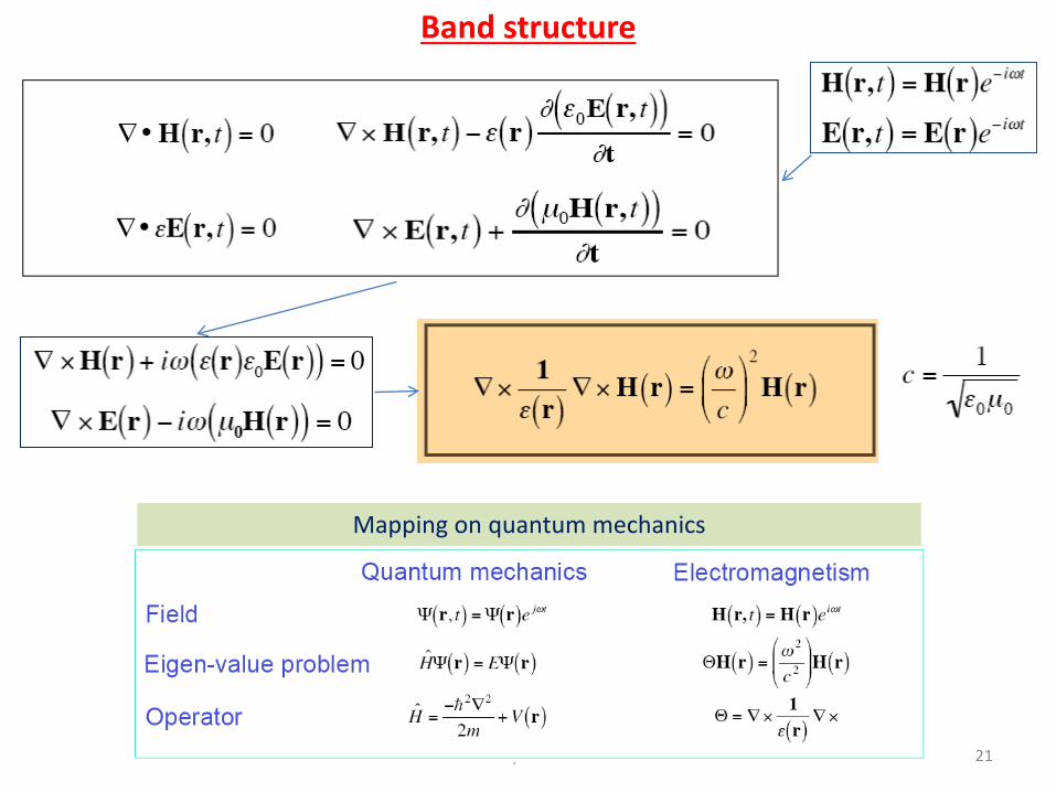
Band structure
21 Nanophotonics
Mapping on quantum mechanics
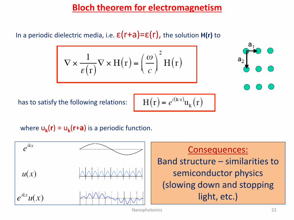
Bloch theorem for electromagnetism
In a periodic dielectric media, i.e. ε(r+a)=ε(r), the solution H(r) to
has to satisfy the following relations:
where uk(r) = uk(r+a) is a periodic function.
22 Nanophotonics
Consequences: Band structure – similarities to
semiconductor physics (slowing down and stopping
light, etc.)
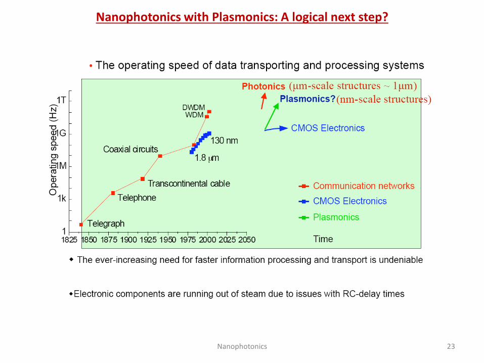
Nanophotonics with Plasmonics: A logical next step?
23 Nanophotonics
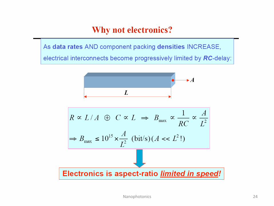
24 Nanophotonics
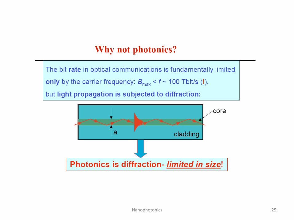
25 Nanophotonics
Nanophotonics 26
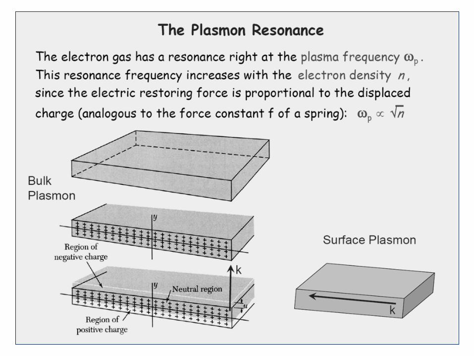
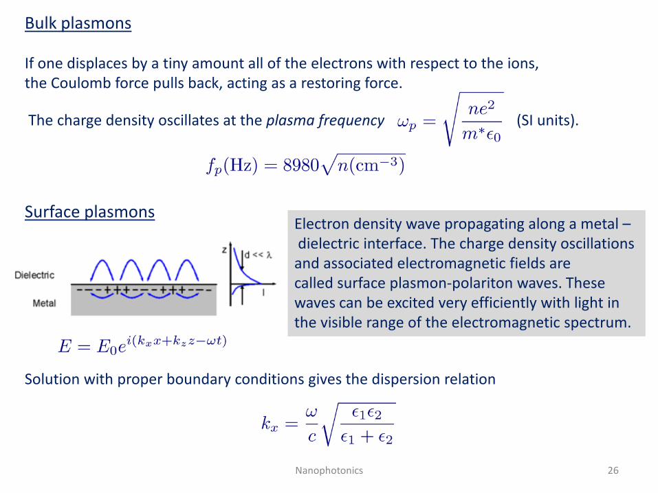
Bulk plasmons
If one displaces by a tiny amount all of the electrons with respect to the ions, the Coulomb force pulls back, acting as a restoring force.
The charge density oscillates at the plasma frequency (SI units).
Surface plasmons Electron density wave propagating along a metal – dielectric interface. The charge density oscillations and associated electromagnetic fields are called surface plasmon-polariton waves. These waves can be excited very efficiently with light in the visible range of the electromagnetic spectrum.
Solution with proper boundary conditions gives the dispersion relation
Nanophotonics 27
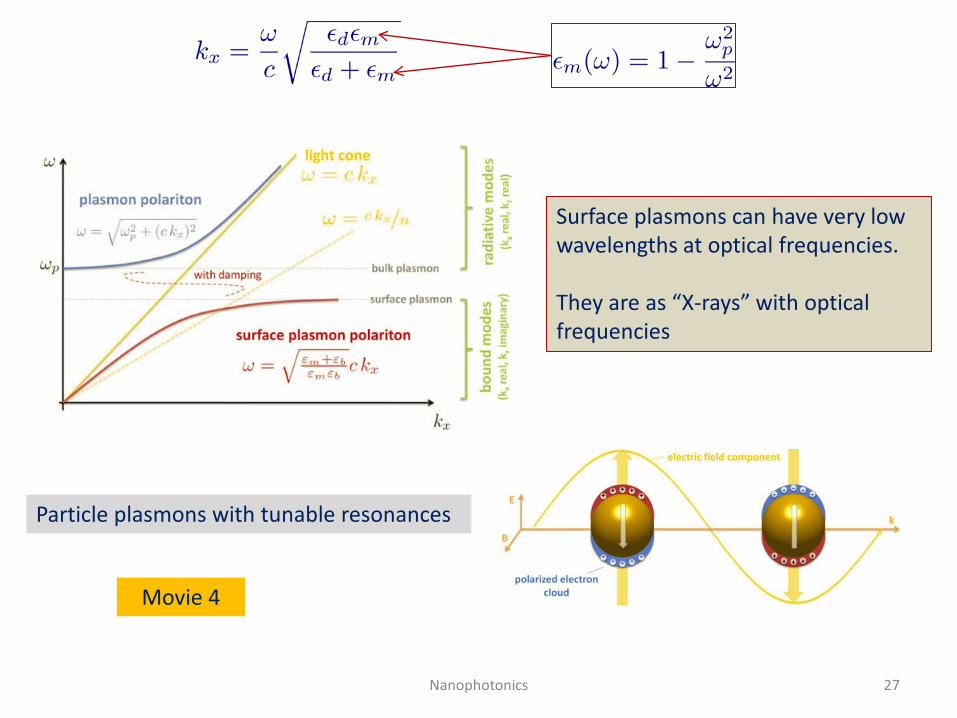
Surface plasmons can have very low wavelengths at optical frequencies. They are as “X-rays” with optical frequencies
Particle plasmons with tunable resonances
Movie 4
28 Nanophotonics
• Photonic crystals are attractive optical materials for controlling and manipulating the flow of light.
• One-dimensional photonic crystals are already in widespread use in the form of thin-film optics with applications ranging from low and high reflection coatings on lenses and mirrors to color changing paints and inks.
• Higher dimensional photonic crystals are of great interest for both fundamental and applied research, and the two dimensional ones are beginning to find commercial applications. The first commercial products involving two-dimensionally periodic photonic crystals are already available in the form of photonic-crystal fibers, which use a microscale structure to confine light with radically different characteristics compared to conventional optical fiber for applications in nonlinear devices and guiding exotic wavelengths.
• The three-dimensional counterparts are still far from commercialization but offer additional features possibly leading to new device concepts (e.g. optical computers), when some technological aspects such as manufacturability and principal difficulties such as disorder are under control.
Summary
29 Nanophotonics
and many other books
Very important new research area …
30 Nanophotonics
Movie 5
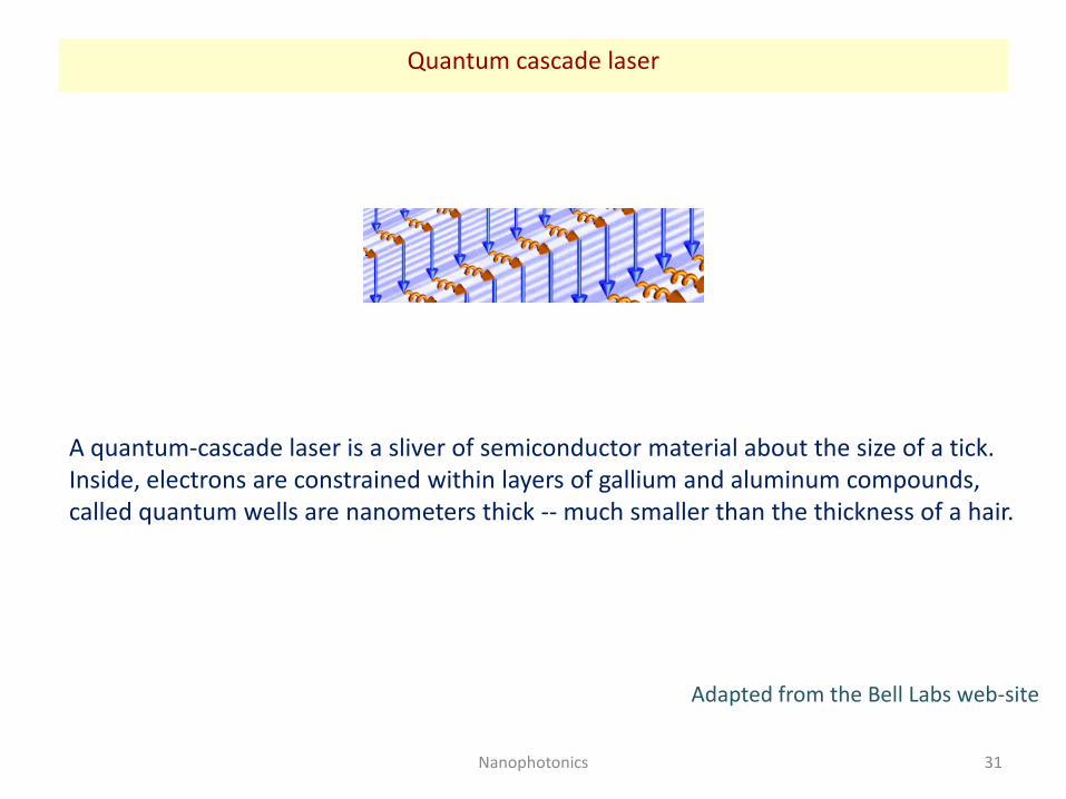
Quantum cascade laser
A quantum-cascade laser is a sliver of semiconductor material about the size of a tick. Inside, electrons are constrained within layers of gallium and aluminum compounds, called quantum wells are nanometers thick -- much smaller than the thickness of a hair.
Adapted from the Bell Labs web-site
31 Nanophotonics
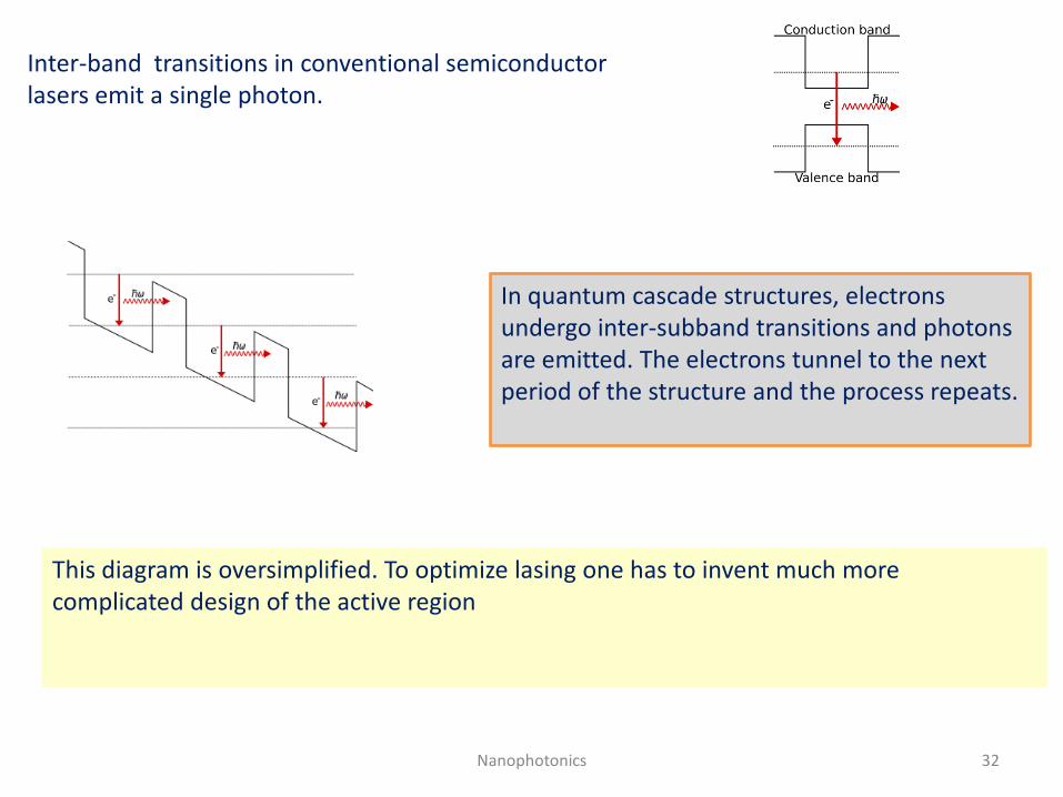
Inter-band transitions in conventional semiconductor lasers emit a single photon.
In quantum cascade structures, electrons undergo inter-subband transitions and photons are emitted. The electrons tunnel to the next period of the structure and the process repeats.
This diagram is oversimplified. To optimize lasing one has to invent much more complicated design of the active region
32 Nanophotonics
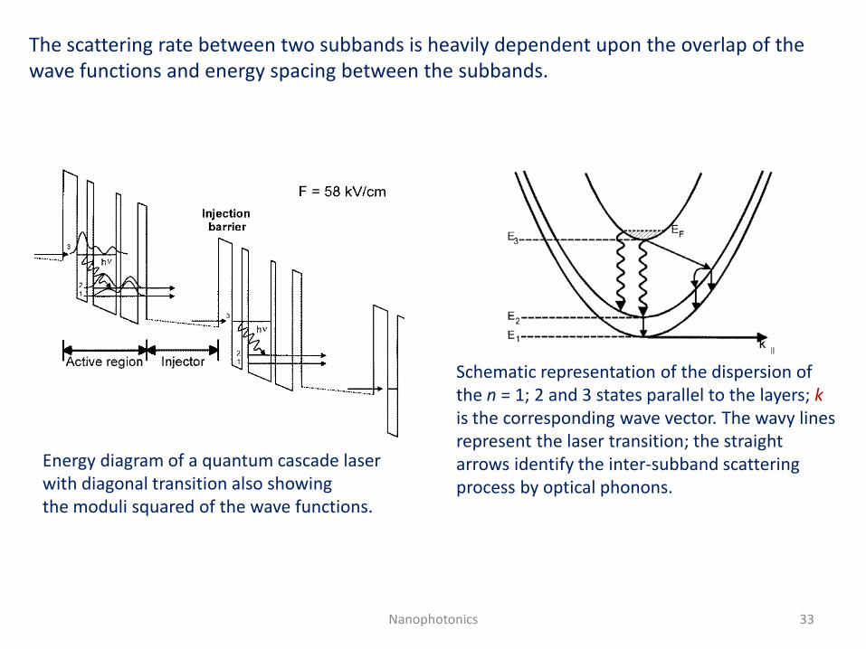
The scattering rate between two subbands is heavily dependent upon the overlap of the wave functions and energy spacing between the subbands.
Energy diagram of a quantum cascade laser with diagonal transition also showing the moduli squared of the wave functions.
Schematic representation of the dispersion of the n = 1; 2 and 3 states parallel to the layers; k is the corresponding wave vector. The wavy lines represent the laser transition; the straight arrows identify the inter-subband scattering process by optical phonons.
33 Nanophotonics
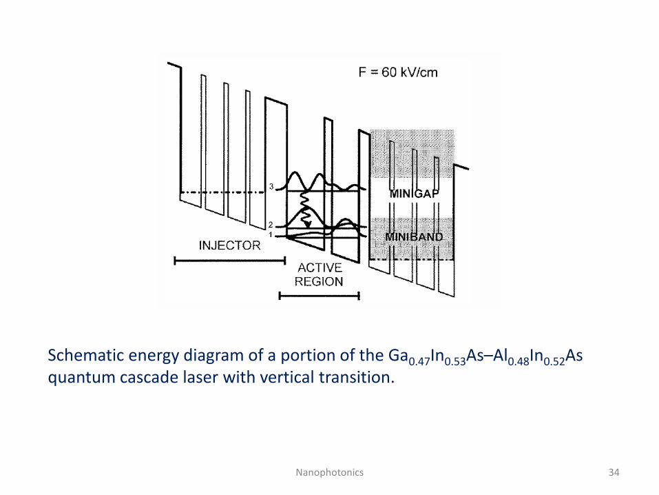
Schematic energy diagram of a portion of the Ga0.47In0.53As–Al0.48In0.52As quantum cascade laser with vertical transition.
34 Nanophotonics
35 Nanophotonics
“The quantum cascade (QC) laser is an excellent example of how quantum engineering can be used to design new laser materials and related light emitters in the mid-IR. The population inversion occurs between excited subbands of coupled quantum wells and is designed by tailoring the electron inter-subband scattering times. This tailoring adds an important dimension to the quantum engineering of heterostructures. The pumping mechanism is provided by injecting electrons into the upper state of the laser transition by resonant tunneling through a potential barrier.”
From Sirtori et al., 1998
36 Nanophotonics