Embed Size (px)
Citation preview

This article was downloaded by: 10.3.98.104On: 11 Feb 2022Access details: subscription numberPublisher: CRC PressInforma Ltd Registered in England and Wales Registered Number: 1072954 Registered office: 5 Howick Place, London SW1P 1WG, UK
6 Handbook of NanophysicsNano Electronics and NanophotonicsKlaus D. Sattler
Carbon Nanotube Memory Elements
Publication detailshttps://www.routledgehandbooks.com/doi/10.1201/9781420075519-5
Vincent. Meunier, Bobby. G. SumpterPublished online on: 17 Sep 2010
How to cite :- Vincent. Meunier, Bobby. G. Sumpter. 17 Sep 2010, Carbon Nanotube MemoryElements from: 6 Handbook of Nanophysics, Nano Electronics and Nanophotonics CRC PressAccessed on: 11 Feb 2022https://www.routledgehandbooks.com/doi/10.1201/9781420075519-5
PLEASE SCROLL DOWN FOR DOCUMENT
Full terms and conditions of use: https://www.routledgehandbooks.com/legal-notices/terms
This Document PDF may be used for research, teaching and private study purposes. Any substantial or systematic reproductions,re-distribution, re-selling, loan or sub-licensing, systematic supply or distribution in any form to anyone is expressly forbidden.
The publisher does not give any warranty express or implied or make any representation that the contents will be complete oraccurate or up to date. The publisher shall not be liable for an loss, actions, claims, proceedings, demand or costs or damageswhatsoever or howsoever caused arising directly or indirectly in connection with or arising out of the use of this material.

Dow
nloa
ded
By:
10.
3.98
.104
At:
16:2
3 11
Feb
202
2; F
or: 9
7814
2007
5519
, cha
pter
3, 1
0.12
01/9
7814
2007
5519
-5
3-1
3.1 Introduction
An incredibly rapid expansion in the demand of portable consumer electronics ranging from personal computers, cellu-lar phones, MP3 players, digital cameras, PDAs, USB memory sticks to applications in the networking arena continues to drive the pursuit for the development of higher density, faster, more efficient, and economical electronic memory devices (Scott 2004). Currently, most commercially available memory elements consist of dynamic random access memory (DRAM), static random access memory (SRAM), or flash memory (non-volatile memory). DRAM is considered to be very fast and cheap but its contents are lost when power is switched off (vola-tility). SRAM is much faster and needs less power but is far more expensive and also suffers from volatility. Flash memory is nonvolatile but currently operates at low write speed and thus has a slow random access. In addition, it is power-hungry and very expensive. In the past, incremental improvements in memory capacity and capability were primarily achieved by the simple scaling of the physical dimensions of the devices. However, the semiconductor industry is quickly reaching the fundamental limits on the miniaturization, encountering, for example, extreme difficulties due to short channel effects in the scaling of metal-oxide-semiconductor field-effect transistor
(MOSFET). This difficulty has stimulated an intense growth in research and development in the area of new technologies and materials that can overcome these limitations and deliver unprecedented capabilities for memory storage and access. Some promising new types of memory-storage devices include magnetoresistive RAM (MRAM), ferroelectric RAM (FRAM), phase-change memory (PRAM), and novel high speed–density nonvolatile memory (these are primarily based on carbon nanotubes [CNTs]) (Waser 2003).
CNT-based data-storage devices or memory elements offer high potential for considerable improvements compared to cur-rent memory paradigms (Bichoutskaia et al. 2008, Zhang 2006). First, CNTs are considerably smaller than conventional cells, e.g., each nanotube is less than 1/10,000th the width of a human hair, thus allowing an impressive density to be achieved in a modest space. The intrinsic structural, thermal, and mechanical stability of CNTs are expected to confer to these memory devices a very long lifetime while the power requirements for their operation should be considerably less than DRAM. In addition, CNTs are known to be radiation-resistant and nanotube-based memory elements are therefore expected to be robust in numer-ous types of environments. As such, these novel types of mem-ory elements have recently been touted as a “universal memory” (Bichoutskaia et al. 2008).
3Carbon Nanotube Memory Elements
3.1 Introduction .............................................................................................................................3-13.2 CNFET-Based Memory Elements .........................................................................................3-2
General Description of a CNFET • FET-Based Memory Elements: Pioneering Works • FET-Based Memory Elements: Further Improvements • FET-Based Memory Elements: Controlling Storage Nodes • FET-Based Memory Elements: Optoelectronic Memory • Redox Active Molecules as Storage Nodes • Two-Terminal Memory Devices • Using Nanotubes as Storage Nodes • Conclusions
3.3 NEMS-Based Memory ............................................................................................................3-9NEMS: Generalities • Carbon Nanotube Crossbars for Nonvolatile Random Access Memory Applications • Nanorelays • Feedback-Controlled Nanocantilevers • Data Storage Based on Vertically Aligned Carbon Nanotubes • Linear Bearing Nanoswitch • Conclusions
3.4 Electromigration CNT-Based Data Storage ...................................................................... 3-16A “Bucky Shuttle” Memory Element • Memory Elements Based on the “Bucky Shuttle” Concept • Conclusions
3.5 General Conclusions ............................................................................................................. 3-18Acknowledgments ............................................................................................................................. 3-18References ...........................................................................................................................................3-19
Vincent MeunierOakRidgeNationalLaboratory
Bobby G. SumpterOakRidgeNationalLaboratory
Dow
nloa
ded
By:
10.
3.98
.104
At:
16:2
3 11
Feb
202
2; F
or: 9
7814
2007
5519
, cha
pter
3, 1
0.12
01/9
7814
2007
5519
-53-2 HandbookofNanophysics:NanoelectronicsandNanophotonics
In this chapter, we review the developments in memory ele-ments that exploit the properties of CNTs. These nanoscale sys-tems fit into the realm of nanoelectronics and offer exceptional properties and well-characterized structures that have rapidly emerged as a viable route to satisfy the future requirements and needs for data-storage and memory devices. Given the difficulty in the integration of nanoscale systems, such as CNTs, into ade-quate arrangements for useful structures and devices, and the complexity in the assessment of the properties of the devices, a tremendous effort has been devoted in the past years toward the development of experimental and theoretical methods mak-ing it possible to creatively imagine, design, and test new sys-tems for desired and tailored characteristics. In this chapter, we review the different types of CNT-based memory devices, which include memory elements based on CNT field-effect transistors (CNFET) (Section 3.2), nanoelectromechanical systems (NEMS) (Section 3.3), and electromigration (Section 3.4). The fundamen-tal operational principles and characteristics of the different devices and concepts are examined in detail along with a discus-sion of the current status of experimental fabrication and practi-cal realization.
3.2 CNFEt-Based Memory Elements
A number of CNT memory elements have been developed from the functioning principle of CNFETs. The following section will be devoted to a description of a few of them. First, we will expose
the basic working principle of the CNFET before showing how CNFETs can be implemented for memory applications.
3.2.1 General Description of a CNFEt
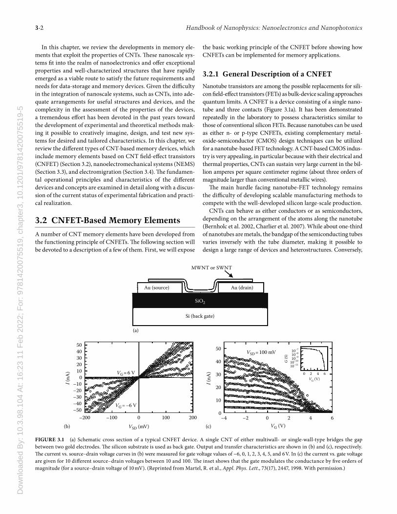
Nanotube transistors are among the possible replacements for sili-con field-effect transistors (FETs) as bulk-device scaling approaches quantum limits. A CNFET is a device consisting of a single nano-tube and three contacts (Figure 3.1a). It has been demonstrated repeatedly in the laboratory to possess characteristics similar to those of conventional silicon FETs. Because nanotubes can be used as either n- or p-type CNFETs, existing complementary metal-oxide-semiconductor (CMOS) design techniques can be utilized for a nanotube-based FET technology. A CNT-based CMOS indus-try is very appealing, in particular because with their electrical and thermal properties, CNTs can sustain very large current in the bil-lion amperes per square centimeter regime (about three orders of magnitude larger than conventional metallic wires).
The main hurdle facing nanotube-FET technology remains the difficulty of developing scalable manufacturing methods to compete with the well-developed silicon large-scale production.
CNTs can behave as either conductors or as semiconductors, depending on the arrangement of the atoms along the nanotube (Bernholc et al. 2002, Charlier et al. 2007). While about one-third of nanotubes are metals, the bandgap of the semiconducting tubes varies inversely with the tube diameter, making it possible to design a large range of devices and heterostructures. Conversely,
Si (back gate)
(a)
SiO2
Au (source) Au (drain)
MWNT or SWNT
5040302010
0
50
40
30
20
10–7
10–8
10–9
10–10
10–11
0 2VG (V)
G (S
)
4 6
10
0
–10–20–30–40–50
–200 –4 –2 0 2 4 6–100 0VSD (mV)(b) (c)
I (nA
)
I (nA
)
VG (V)
VSD = 100 mV
VG = –6 V
VG = 6 V
100 200
FIGURE 3.1 (a) Schematic cross section of a typical CNFET device. A single CNT of either multiwall- or single-wall-type bridges the gap between two gold electrodes. The silicon substrate is used as back gate. Output and transfer characteristics are shown in (b) and (c), respectively. The current vs. source–drain voltage curves in (b) were measured for gate voltage values of −6, 0, 1, 2, 3, 4, 5, and 6 V. In (c) the current vs. gate voltage are given for 10 different source–drain voltages between 10 and 100. The inset shows that the gate modulates the conductance by five orders of magnitude (for a source–drain voltage of 10 mV). (Reprinted from Martel, R. et al., Appl. Phys. Lett., 73(17), 2447, 1998. With permission.)
Dow
nloa
ded
By:
10.
3.98
.104
At:
16:2
3 11
Feb
202
2; F
or: 9
7814
2007
5519
, cha
pter
3, 1
0.12
01/9
7814
2007
5519
-5CarbonNanotubeMemoryElements 3-3
conducting nanotubes possess a very low resistance for electron flow (ballistic conductors) because the decoherence length of the nanotube wavefunctions is typically larger than practical nano-tube lengths. As long as the nanotube length is shorter than the decoherence length, the resistance will not depend upon the cyl-inder length. In that case, the only electrical resistance is at the contact points where the electrons enter and leave the tube. As shown below, it is precisely at the interface between the nanotube and the metallic electrodes that the physical processes responsible for the functioning of a nanotube transistor take place.
CNFETs can be fabricated with a structure very similar to silicon FETs. As shown in Figure 3.1a, such a device consists of a single-walled semiconducting nanotube whose ends are attached to two metallic contacts. In the terminology of transis-tors, the nanotube acts as the channel and the two contacts are the drain and the source, respectively. The device is completed by a gate electrode that is positioned somewhere between the source and the drain. There are a number of possible designs: the nanotube can be positioned above or under the metallic contacts and the gate can be placed as a back or front gate. For a transis-tor to work properly the semiconductor CNT must be doped. In air, at room temperature, the device behaves as a depletion mode p-FET (the I–V is typical of hole conduction, Figure 3.1b). The transistor action is due to the electric field around the gate modulating the Schottky barrier at the points where the source and drain terminals contact the nanotube. For reasonably short tubes (a few hundred nanometers or less), the effect of the gate voltage on channel resistance is minimal. Experimentally, the first-reported CNFETs were all p-type devices. This is because when exposed to air, nanotubes are p-doped due to the pres-ence of oxygen that shifts the Fermi level at the metal–nanotube interface toward the valence band, leading to a hole-conduction mechanism. When the same device is heated in a vacuum and allowed to outgas, the Fermi level shifts toward the conduction band, which leads to an electron-conduction mechanism, i.e., acts as an n-type FET. Different types of FETs can be obtained
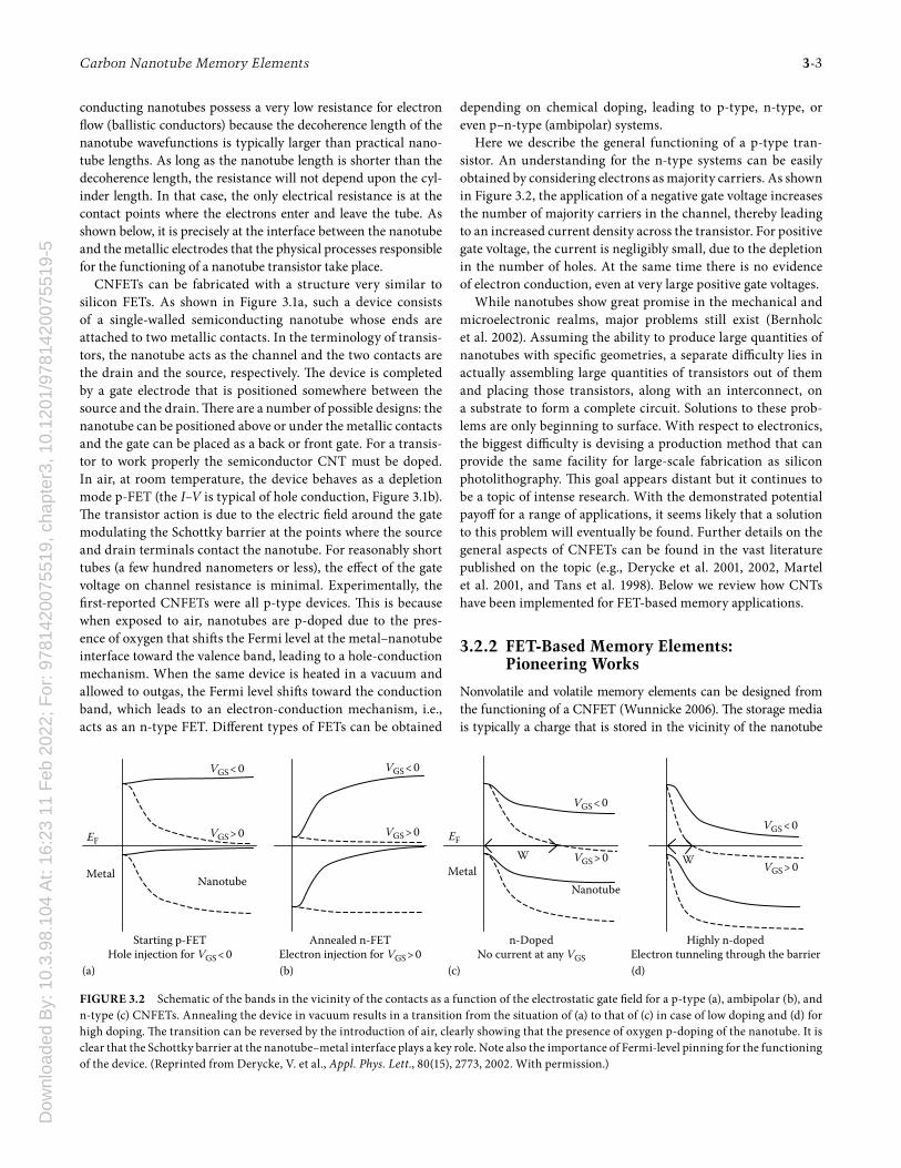
depending on chemical doping, leading to p-type, n-type, or even p–n-type (ambipolar) systems.
Here we describe the general functioning of a p-type tran-sistor. An understanding for the n-type systems can be easily obtained by considering electrons as majority carriers. As shown in Figure 3.2, the application of a negative gate voltage increases the number of majority carriers in the channel, thereby leading to an increased current density across the transistor. For positive gate voltage, the current is negligibly small, due to the depletion in the number of holes. At the same time there is no evidence of electron conduction, even at very large positive gate voltages.
While nanotubes show great promise in the mechanical and microelectronic realms, major problems still exist (Bernholc et al. 2002). Assuming the ability to produce large quantities of nanotubes with specific geometries, a separate difficulty lies in actually assembling large quantities of transistors out of them and placing those transistors, along with an interconnect, on a substrate to form a complete circuit. Solutions to these prob-lems are only beginning to surface. With respect to electronics, the biggest difficulty is devising a production method that can provide the same facility for large-scale fabrication as silicon photolithography. This goal appears distant but it continues to be a topic of intense research. With the demonstrated potential payoff for a range of applications, it seems likely that a solution to this problem will eventually be found. Further details on the general aspects of CNFETs can be found in the vast literature published on the topic (e.g., Derycke et al. 2001, 2002, Martel et al. 2001, and Tans et al. 1998). Below we review how CNTs have been implemented for FET-based memory applications.
3.2.2 FEt-Based Memory Elements: Pioneering Works
Nonvolatile and volatile memory elements can be designed from the functioning of a CNFET (Wunnicke 2006). The storage media is typically a charge that is stored in the vicinity of the nanotube
Metal
EF
VGS < 0
VGS > 0VGS > 0
Nanotube
(a) (b)
Starting p-FETHole injection for VGS < 0
Annealed n-FETElectron injection for VGS > 0
VGS < 0
EF
VGS > 0VGS > 0WW
VGS < 0
VGS < 0
Nanotube
n-DopedNo current at any VGS
Highly n-dopedElectron tunneling through the barrier(d)(c)
Metal
FIGURE 3.2 Schematic of the bands in the vicinity of the contacts as a function of the electrostatic gate field for a p-type (a), ambipolar (b), and n-type (c) CNFETs. Annealing the device in vacuum results in a transition from the situation of (a) to that of (c) in case of low doping and (d) for high doping. The transition can be reversed by the introduction of air, clearly showing that the presence of oxygen p-doping of the nanotube. It is clear that the Schottky barrier at the nanotube–metal interface plays a key role. Note also the importance of Fermi-level pinning for the functioning of the device. (Reprinted from Derycke, V. et al., Appl. Phys. Lett., 80(15), 2773, 2002. With permission.)

Dow
nloa
ded
By:
10.
3.98
.104
At:
16:2
3 11
Feb
202
2; F
or: 9
7814
2007
5519
, cha
pter
3, 1
0.12
01/9
7814
2007
5519
-53-4 HandbookofNanophysics:NanoelectronicsandNanophotonics
channel. The charge causes a threshold potential shift (the threshold potential is defined as the potential at which the majority carriers start flowing) of the nanotube FET. Because the nanotube has very high carrier mobility, the information can be stored in a few (as few as one) electrons configuration. The states can be reversibly written and erased. The reading mechanism is performed via a measure-ment of the source–drain current, while the writing mechanism is completed using a large bias voltage applied to the gate.
A number of groups have obtained convincing results on CNFET-based memory elements. How the information is stored and consequently under which conditions the memory is usable depends on the details of the manufacturing, particularly in the gating material. The first two examples of FET-memory ele-ments were proposed independently by Fuhrer et al. (2002) and Radosavljevic et al. (2002). The functioning of the devices hinges on the operation of a single-electron memory. In this case, the capacitance of the storage node must be small enough so that its Coulomb-charging energy is significantly larger than the thermal energy at the operating temperature, and the readout device must be sensitive enough to detect a single nearby electronic charge. In
Fuhrer’s device, the charge is reversibly injected and removed from the dielectric (placed between the tube and the gate electrode) by applying a moderate (10 V) bias between the nanotube and the substrate. The nanotube is ideal as a charge-detecting device due to its high carrier mobility, large geometrical capacitance, and its one-dimensional (1D) nature ensuring that local changes in charge affects the global conductance (due to slow screening). In Fuhrer’s pioneering work, for instance, discrete charge states cor-responding to differences of a single, or at most a few, stored elec-trons are observed. The device is based on the characteristics of a p-type FET (i.e., it conducts at negative gate voltage and becomes insulating at positive gate voltage) and can be operated at temper-atures up to 100 K. Properties relevant to memory operation are demonstrated by the large hysteresis I–Vg curve that is obtained by sweeping the gate voltage Vg between −10 and +10 V. As is shown in Figure 3.3, the threshold voltage is shifted by more than 6 V. The mechanism of charge storage is related to the rearrangement of charges in the dielectric or by the injection or removal of charges from the dielectric through the electrodes or the nanotube. Due to the geometry of the device, the electric field at the surface of the
2
1
08
0
–8
100 200 300Time (s)(c)
V g (V
)I sd
(μA
)
400 500
Erase
Read
Write0
1
3.0
2.5
2.0
1.5
1.0
0.5
0.0
Vg (V)(a) (b)
I sd (μ
A)
–10 –5 0 5 10
FIGURE 3.3 (a) Atomic force microscope topographic image of the nanotube device used in Fuhrer et al. (2002). The nanotube extends between the two dark blocks at the top and bottom of the image (i.e., the electrodes). The scale bar represents 1 μm. (b) Drain current as a function of gate voltage at room temperature and a source–drain bias of 500 mV. As the gate voltage is swept from positive to negative and back, a strong hysteresis is observed, as indicated by the arrows denoting the sweep direction. (c) Series of four read–write cycles of the nanotube memory at room tempera-ture. The upper panel shows the drain current at a source–drain bias of 500 mV, while the lower panel shows the gate voltage. The memory state was read at −1 V, and written with pulses of ±8 V. (Reprinted from Fuhrer, M.S. et al., Nano Lett., 2(7), 755, 2002. With permission.)
Dow
nloa
ded
By:
10.
3.98
.104
At:
16:2
3 11
Feb
202
2; F
or: 9
7814
2007
5519
, cha
pter
3, 1
0.12
01/9
7814
2007
5519
-5CarbonNanotubeMemoryElements 3-5
nanotube is very large, at least large enough to cause the move-ment of charge in the dielectric (Fuhrer et al. evaluated the field to be comparable to the breakdown field in SiO2). At these high fields the electrons are easily injected into the dielectric from the nanotube and remain trapped in metastable states until the polar-ity is reversed.
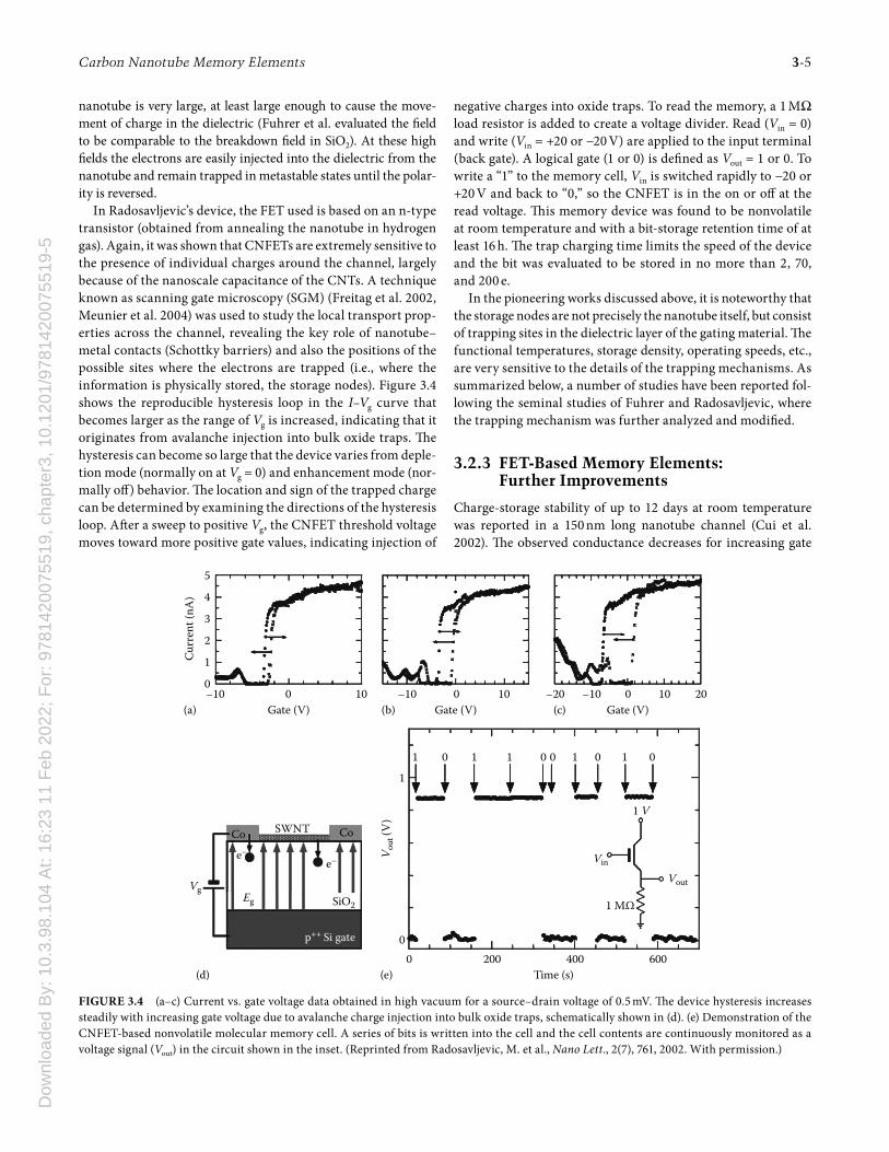
In Radosavljevic’s device, the FET used is based on an n-type transistor (obtained from annealing the nanotube in hydrogen gas). Again, it was shown that CNFETs are extremely sensitive to the presence of individual charges around the channel, largely because of the nanoscale capacitance of the CNTs. A technique known as scanning gate microscopy (SGM) (Freitag et al. 2002, Meunier et al. 2004) was used to study the local transport prop-erties across the channel, revealing the key role of nanotube–metal contacts (Schottky barriers) and also the positions of the possible sites where the electrons are trapped (i.e., where the information is physically stored, the storage nodes). Figure 3.4 shows the reproducible hysteresis loop in the I–Vg curve that becomes larger as the range of Vg is increased, indicating that it originates from avalanche injection into bulk oxide traps. The hysteresis can become so large that the device varies from deple-tion mode (normally on at Vg = 0) and enhancement mode (nor-mally off) behavior. The location and sign of the trapped charge can be determined by examining the directions of the hysteresis loop. After a sweep to positive Vg, the CNFET threshold voltage moves toward more positive gate values, indicating injection of
negative charges into oxide traps. To read the memory, a 1 MΩ load resistor is added to create a voltage divider. Read (Vin = 0) and write (Vin = +20 or −20 V) are applied to the input terminal (back gate). A logical gate (1 or 0) is defined as Vout = 1 or 0. To write a “1” to the memory cell, Vin is switched rapidly to −20 or +20 V and back to “0,” so the CNFET is in the on or off at the read voltage. This memory device was found to be nonvolatile at room temperature and with a bit-storage retention time of at least 16 h. The trap charging time limits the speed of the device and the bit was evaluated to be stored in no more than 2, 70, and 200 e.
In the pioneering works discussed above, it is noteworthy that the storage nodes are not precisely the nanotube itself, but consist of trapping sites in the dielectric layer of the gating material. The functional temperatures, storage density, operating speeds, etc., are very sensitive to the details of the trapping mechanisms. As summarized below, a number of studies have been reported fol-lowing the seminal studies of Fuhrer and Radosavljevic, where the trapping mechanism was further analyzed and modified.
3.2.3 FEt-Based Memory Elements: Further Improvements
Charge-storage stability of up to 12 days at room temperature was reported in a 150 nm long nanotube channel (Cui et al. 2002). The observed conductance decreases for increasing gate
1
0p++ Si gate
SiO2
SWNT
e–e–
EgVg
Co Co
0
1 0 0 0 0 01 1 1 1
1 V
Vin
Vout
1 MΩ
200 400Time (s)(e)(d)
V out
(V)
600
5
4
3
2
Curr
ent (
nA)
1
0–10 0
Gate (V)(a) (b) (c)Gate (V) Gate (V)10 –10 0 10 –10–20 0 10 20
FIGURE 3.4 (a–c) Current vs. gate voltage data obtained in high vacuum for a source–drain voltage of 0.5 mV. The device hysteresis increases steadily with increasing gate voltage due to avalanche charge injection into bulk oxide traps, schematically shown in (d). (e) Demonstration of the CNFET-based nonvolatile molecular memory cell. A series of bits is written into the cell and the cell contents are continuously monitored as a voltage signal (Vout) in the circuit shown in the inset. (Reprinted from Radosavljevic, M. et al., Nano Lett., 2(7), 761, 2002. With permission.)
Dow
nloa
ded
By:
10.
3.98
.104
At:
16:2
3 11
Feb
202
2; F
or: 9
7814
2007
5519
, cha
pter
3, 1
0.12
01/9
7814
2007
5519
-53-6 HandbookofNanophysics:NanoelectronicsandNanophotonics
potential, a normal feature of p-type, air-exposed single-wall carbon nanotubes (SWCNTs). The hysteresis loop is obtained by sweeping continuously the gate voltage from −3 to +3 V. This shows two conductance states at Vg = 0 differing by more than two orders of magnitude, associated with a threshold voltage of 1.25 V. The method used by Cui et al. is more technologically straightforward compared to the previously reported techniques, as it does not require separating SWCNT bundles into indi-vidual SWCNTs during sample preparation. The sample treat-ment is likely to be responsible for the modified type of trapping centers, compared to earlier similar devices. The heat treatment and exposure to oxygen plasma cause the metallic nanotubes present in the bundle to be preferentially oxidized, leading to increased gate dependence due to the remaining intact semicon-ducting tubes. In addition, oxidation-related defects are likely to be formed in the remaining amorphous carbon particles on the bundle surface or at the SiO2 interface. These defects act as charge-storage traps and their close proximity to the surface of the channel accounts for the large threshold voltage shifts.
Another type of charge trapping was presented by Kim et al. (2003). In that case, water molecules were shown to be responsi-ble for the hysteresis properties (i.e., responsible for the threshold potential shift) of the I–Vg curves. The water molecules contrib-uting to the trapping could be located on the nanotube surface or on the SiO2 close to the tube. Heating under dry conditions significantly reduces the hysteresis. A completely hysteresis-free CNFET was possible by passivation of the device using a polymer coating, clearly indicating that the storage nodes were removed by the treatment. This work also confirms the central role played by surface chemistry on the properties of the device and that truly robust passivation is needed in order to use CNT-based devices in practical electronic devices, unless it is simply used as a detection device (e.g., of humidity).
More recent work of Yang et al. confirmed the role of adsorbed (including water and alcohol) molecules for charge trapping, also showing charge retention of up to 7 days under ambient conditions (Yang et al. 2004).
3.2.4 FEt-Based Memory Elements: Controlling Storage Nodes
Soon after the publication of the pioneering works of 2002, a number of groups confirmed that the as-prepared nanotube FETs possessed intrinsic charge-trapping centers that were responsible for the shift in the threshold voltage measured in the hysteresis loop of the I–Vg characteristics. As discussed briefly above, the trapping centers can be defects in the SiO2, water, or alcohol molecules adsorbed on the tube or the dielectric, or oxi-dized amorphous carbon. It was soon understood that a better control of the storage medium was required in order to harness the full potential of CNFET-based memory elements.
In 2003, Choi et al. proposed a SWCNT nonvolatile mem-ory device using SiO2-Si3N4-SiO2 (ONO) layers as the storage node (Choi et al. 2003). In that device, the top gate structure is placed above the ONO layer, which is positioned directly above
a few-nanometers-long channel. Charges can tunnel from the CNT surface into the traps present in the ONO layers. The stored charges impose a threshold voltage shift of 60 mV, which is independent of charging time, suggesting that the ONO traps present a quasi-quantized state. The choice of SiO2-Si3N4-SiO2 is motivated by the fact that it presents a high breakdown volt-age, low defect density, and high charge-retention capability (Bachhofer et al. 2001).
Another type of device was demonstrated experimentally in 2005 (Ganguly et al. 2005). In this case, the charge-storage nodes consist of gold nanocrystals placed on the top gate above the nano-tube channel. The device was found to have a large memory win-dow with low voltage operations and single-electron-controlled drain currents. The device is based on a Coulomb blockade behavior, in other words on the difficulty of adding supplemen-tary electrons due to the large charging effect of the system with large capacitance and Coulomb repulsion. The Coulomb block-ade in the nanocrystals, along with the single-charge sensitivity of the nanotube FET, is suggested to allow for multilevel opera-tions. In this device, the reported retention is rather modest: 6200 s at 10 K and only 800 s at room temperature. Better dielec-tric and preprocessing should improve these low retention times.
More recently, Sakurai et al. proposed a modified design where the dielectric insulator was made up of a ferroelectric thin film (Sakurai et al. 2006). The experimental results show that the car-riers in the CNTs are controlled by the spontaneous polarization of the ferroelectric films. Ferroelectric-gate FETs offer potential advantages as nonvolatile memory elements, such as low power consumption, the capability of high-density integration, and nondestructive readable operation. So far, the use of ferroelec-tric thin films in conventional Si-based FETs for memory appli-cations has been complicated because of the extreme difficulty of fabricating the ferroelectric/Si structure with good interface properties due to the chemical reaction and interdiffusion of Si and ferroelectrics. It was suggested that this problem could be resolved by inserting an insulating layer between the ferroelec-tric and the semiconductor layers, but at the cost of increased voltage operation and depolarization field. Another method was to use an oxide semiconductor, such as indium tin oxide. However, even though this system also shows good memory operation, the carrier mobility is much lower than in Si, causing problems that are unacceptable for high-performance nonvola-tile memory elements. The use of a semiconducting tube as the conducting channel and a ferroelectric as a gate insulator allevi-ates all of these problems: the new design allows the carriers in the channel to be controlled by the spontaneous polarization of the ferroelectric film, while keeping the high-conduction char-acteristics of CNTs. In the demonstrated prototypical device, a 400 nm thick PZT (PbZr0.5TiO5O3) film was used. The threshold voltage was found to be shifted in the positive direction when Vg was swept from negative to positive bias and was shifted in the negative direction when Vg was swept from positive to negative. This gave a clear hysteresis loop and bistable current values at Vg = 0, due to the spontaneous polarization of the electric field (the effects of charge trapping in the dielectric was found to be
Dow
nloa
ded
By:
10.
3.98
.104
At:
16:2
3 11
Feb
202
2; F
or: 9
7814
2007
5519
, cha
pter
3, 1
0.12
01/9
7814
2007
5519
-5CarbonNanotubeMemoryElements 3-7
negligible compared to the effects due to the ferroelectric, at least for small sweeping range of Vg).
3.2.5 FEt-Based Memory Elements: Optoelectronic Memory
In all of the CNFET-based memory devices mentioned thus far in this chapter, the information is stored by applying a large enough gate voltage to store or remove the charge in, or from, the traps (for the ferroelectric-based FET, the gate is used to flip the polarization field). In Star’s CNFET-memory (p-type) device, the information is still stored as electric charges (Star et al. 2004), however, it differs in that the writing mechanism relies on the use of optical illumination of a photosensitive polymer (which is part of the gate electrode) that converts photons into electric charge stored in the vicinity of the channel. The infor-mation is read by measuring the source–drain current, while it is erased (the charge is removed) using a large gate voltage. In other words, this optoelectronic memory is written optically and read and erased electrically. The threshold voltage change com-pared to the non-illuminated system was measured to be as large as +2 V after optical excitation, suggesting a charge transfer of about 300 electrons per micron in the tube.
3.2.6 redox active Molecules as Storage Nodes
In this experimentally built system, the overall configuration and operating principle consists of a nanotube or nanowire FET functionalized with redox active molecules, where an applied
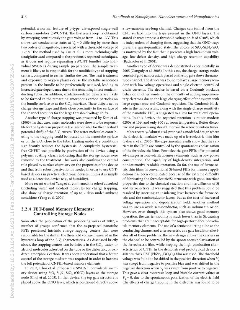
gate voltage or source–drain voltage pulse is used to inject net positive or negative charge into the molecular layer (Duan et al. 2002). The oxide layer, on the surface of the channel, serves as a barrier to reduce charge leakage between the molecules and the channel, and thus maintains the charge state of the redox mol-ecules, thereby guaranteeing nonvolatility. The charged redox molecules gate the FET to a logic on state with higher channel conductance or the off state with lower channel conductance. Positive charges in the redox material act just like a positive gate, leading to an accumulation of electrons and an on state in n-type semiconducting nanowire-based FETs. For p-type FETs, the same effect is obtained with negative charges in the redox layer, which cause an increase in majority carrier density, in this case holes, in the channel (Figure 3.5). Mannick et al. also described a similar device, using SWCNTs as channels, where the conduc-tance is switched on or off, guided by chemical reactivity of a CNT in H2SO4 (Goldsmith et al. 2007, Mannik et al. 2006).
3.2.7 two-terminal Memory Devices
Transistor devices consist of three electrodes: a source, a drain, and a gate terminal. The source and the drain are good met-als (Au, Pt, Co, etc.) and the gate terminal is typically made up of a dielectric layer (e.g., SiO2) sandwiched between the channel and a heavily doped Si-wafer, which is hooked up to the gate battery. The present authors have theoretically pro-posed a modified version of the FET memory device where the physical gate is replaced by a virtual electrode. The role of the
Source Drain
“Write 1”
NanowireRedox molecules
n-Type on
n-Type off
+ + + + + + + + + + + +
+ + + + + + + + + + + +
– – – – – – – – – – – –
– – – – – – – – – – – –
1 μm
“Write 0”
Silicon oxide
Silicon back gate
Semiconductor
Oxide
FIGURE 3.5 Nanowire-based nonvolatile devices. The devices consist of a semiconductor nanowire (NW) configured as a FET with the oxide surface functionalized with redox active molecules. The top-middle inset shows a scanning electron microscope (SEM) image of a device, and the lower circular inset shows a TEM image of an InP NW highlighting the crystalline core and surface oxide. Positive or negative charges are injected into, and stored in, the redox molecules with an applied gate or bias voltage pulse. In an n-type NW, positive charges create an on or logic “1” state, while negative charges produce an off or logic “0” state. (Reprinted from Duan, X.F. et al., Nano Lett., 2(5), 487, 2002. With permission.)
Dow
nloa
ded
By:
10.
3.98
.104
At:
16:2
3 11
Feb
202
2; F
or: 9
7814
2007
5519
, cha
pter
3, 1
0.12
01/9
7814
2007
5519
-53-8 HandbookofNanophysics:NanoelectronicsandNanophotonics
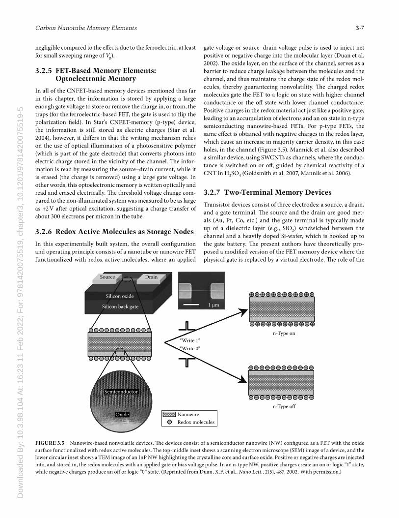
gate is filled by a single donor or acceptor molecule embedded inside a metallic nanotube channel (Meunier and Sumpter 2007, Meunier et al. 2007) (Figure 3.6). The resulting device is a two-terminal system where the conduction properties can be turned on and off by modifying the position of the donor (or acceptor) molecule relative to the nanotube inner core. The intrinsic gating effect works for any nanotube-molecule couple, as long as the molecule possess two stable positions corresponding to a different interacting scheme with the nanotube host (bistability). The gating mechanism works as follows: In one orientation, charge transfer between the mol-ecule and the nanotube imposes a suppression of the current. In another orientation, when the interaction is not only purely electrostatic (charge transfer), but also includes significant directional binding, the gating effect is suppressed and current flow is allowed. It was proposed that the molecule’s orientation can be modified by imposing a lateral stress to the nanotube, changing the local atomic arrangement around the molecule, which in turn results in its flipping. Other optional writing mechanisms include the use of a magnetic field, optoelectron-ics, etc. This example underlines the importance of developing a memory device with a well-defined and well-characterized storage node (here the storage node is a single molecule). It is also a memory device that lies at the boundary of FET-type system and NEMS device, as it involves both transistor-like technology and “moving parts,” on which NEMS are based, as shown in Section 3.3.
Tour and coworkers proposed a memory element, not based on FET operation, but relying on the conformation of a molecule as the storage media (He et al. 2006). The idea is based on the development of a metal-free silicon-molecule-nanotube test bed for exploring the electrical properties of single molecules that demonstrated a useful hysteresis I–V loop for memory storage.
(a)
V
(b)
FIGURE 3.6 (a) Schematic representation of the typical setup used to probe the information stored in the nonvolatile memory element based on the encapsulation of a donor–acceptor molecule inside a metal-lic nanotube. In (a) the system is made up a tetrafluorotetracyano-p-quinodimethane molecule encapsulated inside a (10, 10) armchair nanotube. (b) Examples of bistable orientations of the C=C bond of tetracyanoethylene (TCNE) inside a (9, 0) zigzag CNT. (Reprinted from Meunier, V. and Sumpter, B.G., Nanotechnology, 18(42), 424032, 2007. With permission.)
Metal gate Metal gate
Control oxide (High-k HfAlO dielectric)
Tunneling oxide (High-k HfAlO dielectric)
Si substrate Si substrate
(b)(a)
5 nm
Epoxy
HfAlO
HfAlO
CNT
CNT CNT CNT CNT Interfacial layer
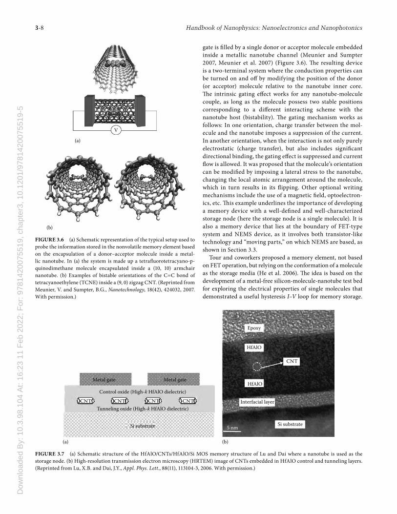
FIGURE 3.7 (a) Schematic structure of the HfAlO/CNTs/HfAlO/Si MOS memory structure of Lu and Dai where a nanotube is used as the storage node. (b) High-resolution transmission electron microscopy (HRTEM) image of CNTs embedded in HfAlO control and tunneling layers. (Reprinted from Lu, X.B. and Dai, J.Y., Appl. Phys. Lett., 88(11), 113104-3, 2006. With permission.)
Dow
nloa
ded
By:
10.
3.98
.104
At:
16:2
3 11
Feb
202
2; F
or: 9
7814
2007
5519
, cha
pter
3, 1
0.12
01/9
7814
2007
5519
-5CarbonNanotubeMemoryElements 3-9
Nonvolatile memory for more than 3 days with cyclability of greater than 1000 read and write–erase operations was obtained for a molecular interface between the Si and SWCNTs consisting of π-conjugated organic molecules. In this case, the hysteresis in the I–V curve resulted from a conductivity change at high-voltage bias. The conduction state could be easily switched from high to low conductivity, by using a +5 V pulse, and makes it possible for the Si-molecule–SWCNT junction to be used as a nonvolatile memory element. The underlying mechanism for the switch-ing was examined and it was concluded that it was not due to a thermoionic process but likely from a tunneling process across the molecule. Akdim and Pachter suggested that the switching in the device may be driven by conformational changes in the molecule upon the application of an electric field and that the nature of the contact at the interface of the SWCNT mat plays an important role in the switching (Akdim and Pachter 2008).
3.2.8 Using Nanotubes as Storage Nodes
Some authors have reported CNFETs, where nanotubes were used as the storage node. Yoneya et al. proposed a 40 K device with a crossed nanotube junction where one of the tubes is used as channel and the other one is used as floating gate (memory-storage node) (Yoneya et al. 2002). In this case it is the large capac-itance property of the nanotube that is exploited. The floating gate is charged and discharged using a back gate. The main dis-advantage of this approach is the requirement of a low operating temperature. Other reports have focused on room-temperature use of CNTs as storage nodes. Most notably, Lu et al. developed FET-based memory elements (Chakraborty et al. 2008, Lu and Dai 2006) in which the nanotubes are embedded inside the gate oxide in the metal oxide semiconductor structures. The memory structure is made up of an HfAlO/CNTs/HfAlO/Si structure. HfAlO was chosen as the tunneling and control oxides in the memory structures because of its promising performance for high-k gate dielectric applications and floating device appli-cations. The schematic structure of a floating-gate memory device using CNTS as the floating gate is shown in Figure 3.7. The p-type substrate is designed as the current channel and the CNTs are designed to be embedded in the HfAlO film and act as the charge-storage nodes. Excellent long-term charge reten-tion characteristics are expected for the memory structure using CNTs as a floating gate due to their hole-trapping characteris-tics, as is demonstrated in Lu and Dai’s papers. While short-term charge retention was not found to be excellent in their prototype device, the memory window was found to remain at a reasonably large value over the long term.
3.2.9 Conclusions
CNFET-based devices for memory applications have received tremendous interest as is witnessed by the numerous published works outlined above. In all the examples presented, the working principle is that the channel of the transistor consists of a doped semiconducting CNT. For all the examples presented above,
with the exception of those shown in Section 3.2.8, the storage node is usually located close to the channel but is not the channel itself, and depends dramatically on the surface chemistry of the dielectric, nanotube, and dielectric–nanotube interface. In those cases, it is the charge injection into the defects or charge traps in the dielectrics or interface responsible for the bistability and the memory properties.
3.3 NEMS-Based Memory
3.3.1 NEMS: Generalities
NEMS are made of electromechanical devices that have critical dimensions from hundreds to few nanometers (Ke and Espinosa 2006a,b). By exploiting nanoscale effects, NEMS offer a number of unique properties, which in some cases can differ significantly from those of the conventional microelectromechanical systems (MEMS). Those properties pave the way to applications such as force sensors, chemical sensors, and ultrahigh frequency resona-tors. For instance, NEMS operate in the microwave range and have a mechanical quality that allows low-energy dissipation, active mass in the femtogram range, unprecedented sensitiv-ity (forces in the attonewton range, mass up to attograms, heat capacities below yoctocalories), power consumption on the order of 10 attowatts, and high integration levels (Ke and Espinosa 2006a,b). The most interesting properties of NEMS arise from the behavior of the active parts, which is typically in the form of cantilevers or doubly clamped beams with nanoscale dimen-sions. In NEMS, the charge controls the mechanical motion, and vice versa. The presence of mechanical motion demands that the moving element to possess high-quality mechanical properties, including high strengths, high Young’s moduli, and low density. While limitations in strength and flexibility compromise the performance of Si-based NEMS actuators, CNTs are better can-didates to realize the full potential of NEMS, in part due to their one-dimensional structure, high aspect ratio, perfect terminated surfaces, and exceptional electronic and mechanical properties. These properties, now complemented by significant advances in growth and manipulation techniques, make CNTs the most promising building blocks for next-generation NEMS (Bernholc et al. 2002, Chakraborty et al. 2007, and Yousif et al. 2008).
A majority of CNT-based NEMS devices exploit the specific propensity of CNTs to respond efficiently to capacitive forces. Capacitive forces can develop between a nanotube and a gate electrode when the presence of a gate potential induces the rear-rangement of a net charge on the nanotube’s surface, which in turn causes the appearance of a capacitance force between the nanotube and the gate. Because the nanotube is very flex-ible, the capacitance force bends the nanotube toward the gate electrode. This phenomenon hinges on two key proper-ties of the nanotube: a large capacitance due to its shape and size and its exceptional mechanical flexibility. In addition to capacitance forces, other forces play a role in nanotube-based NEMS: elastic, van der Waals (vdW), and short-range forces. It is the delicate balance between those forces that makes the

Dow
nloa
ded
By:
10.
3.98
.104
At:
16:2
3 11
Feb
202
2; F
or: 9
7814
2007
5519
, cha
pter
3, 1
0.12
01/9
7814
2007
5519
-53-10 HandbookofNanophysics:NanoelectronicsandNanophotonics
functioning of nanotube-based NEMS possible. Here we review a few examples of NEMS implementation for memory applica-tions. We will discuss crossbar nonvolatile RAM, nano-relays, feedback- controlled nano- cantilevers, electro-actuated multi-walled nanotubes, linear-bearing nano-switches, and telescop-ing nanotube devices.
3.3.2 Carbon Nanotube Crossbars for Nonvolatile random access Memory applications
Rueckes et al. proposed one of the most promising applications of CNTs for memory applications (Rueckes et al. 2000). The device exploits a suspended SWCNT crossbar array for both I/O and switchable bistable elements with well-defined on and off states. The crossbar consists of a set of parallel SWCNTs on a substrate and a set of parallel SWCNTs that are suspended on a periodic array of supports (Figure 3.8). The storage node is found at each place where two nanotubes cross. The bistability is obtained from a balance between the elastic energy (correspond-ing to the bending energy of the tube, having a minimum for a non-bent tube), and the attractive vdW energy (which creates a minimum corresponding to a situation where the upper nano-tube is deflected downward into contact with the lower nano-tube), as shown qualitatively in Figure 3.9. Since one minimum corresponds to a large vertical distance between the two mutu-ally perpendicular arrays (defined roughly by the height of the supports), it corresponds to a situation where no current can flow between the two wires (this is the off state). At the second minimum (roughly 0.34 nm, the distance between two tubes in a bundle), tunneling current is possible as the tube–tube distance is small enough to allow wave-function overlap between the two tubes. The “bent” geometry therefore corresponds to the on state.
The device can be switched between the on and off situation by transiently charging the nanotubes to produce attractive or repulsive electrostatic forces. In the integrated system, electrical contacts are made only at one end of each of the lower and upper sets of the nanoscale wires in the crossbar array, which makes it possible to address many device elements from a limited number of contacts. It was found that there is a wide range of parameters that yield a bistable potential for the proposed device configura-tion. The robustness of the two states suggests: this architecture is tolerant to variations in the structure. The other important feature of this device is the large difference in resistance between the two states (this is the key property of electron tunneling: the
FIGURE 3.8 NRAM device made from a suspended nanotube device architecture with a three-dimensional view of a suspended crossbar array showing four junctions with two elements in the on state and two elements in the off state. The on state corresponds to nanotubes in con-tact and the off state to nanotubes separated. The substrate consists of a conducting layer (dark gray) that terminates in a thin dielectric layer (light gray). The lower nanotubes are supported directly on the dielec-tric film, whereas the upper nanotubes are suspended by periodic inor-ganic or organic supports (gray blocks). A metal electrode, represented by yellow blocks, contacts each nanotube. (Reprinted from Rueckes, T. et al., Science, 289(5476), 94, 2000. With permission.)
(a)
(b) Tube-tube distance
Tube-tube distance
Pote
ntia
l ene
rgy
Pote
ntia
l ene
rgy
Tube deformation energy
van der Waals interaction
(c) Tube-tube distance
Pote
ntia
l ene
rgy
Total energy
Bistability
FIGURE 3.9 Interaction energies between two SWCNTs (one top and one bottom) in the device shown in Figure 3.8. (a) Mechanical strain in the top nanotube and (b) attractive van der Waals interac-tion, showing a minimum at the nanotube–nanotube distance of about 0.34 nm. Plot in (c) shows the resulting bi-stable potential well used for storing information. The first minimum is in the on state (con-tact) and the second minimum is the off state (physical separation). The existence of the energy barrier between the two minima ensures nonvolatility.
Dow
nloa
ded
By:
10.
3.98
.104
At:
16:2
3 11
Feb
202
2; F
or: 9
7814
2007
5519
, cha
pter
3, 1
0.12
01/9
7814
2007
5519
-5CarbonNanotubeMemoryElements 3-11
tunneling resistance decreases exponentially with the separa-tion), which makes the device operation very reliable. The main drawback of the proposed geometry remains however, that at such small dimensions, the junction gap size imposes significant challenges in the nanofabrication of parallel device arrays.
The concept proposed by Rueckes et al. was further devel-oped by the Nantero company, which has devoted a particu-lar important effort toward integrating nanotube array-based memory devices for practical applications. In an IEEE com-munication in 2004, Ward and coworkers improved the initial device by proposing a novel technique to overcome the hurdle of manipulating individual nanotube structures at the molecu-lar level (Ward et al. 2004). This technique allows CNT-based NEMS devices to be fabricated directly on existing production CMOS fabrication lines. The approach relies on the deposition and lithographic patterning of a 1–2 nm thick fabric of nano-tubes, which retain their molecular-scale electromechanical characteristics, even when patterned with 80 nm feature sizes. Because the nonvolatile memory elements are created in an all-thin-film process, it can be monolithically integrated directly within existing CMOS circuitry to facilitate addressing and readout. The transfer of the NRAM fabrication process to a commercial CMOS foundry is ongoing, and, when commer-cialized, will be the first actual application of CNTs for their unique electronic properties.
A modified NEMS switch using a suspended CNT was stud-ied by Cha et al. (2005). In that memory element, the device has a triode structure and is designed so that a suspended CNT is mechanically switched to one of two self-aligned elec-trodes by repulsive electrostatic forces between the tube and the other self-aligned nanotube electrodes. One of the self-aligned electrodes is set as the source electrode and the third is the gate electrode. The nanotube is suspended between the two other electrodes (acting as a drain electrode). As the gate bias increases, the force between the gate and the drain elec-trode deflects the suspended CNT toward the source electrode and establishes electric contact, which results in current flow between the source and the drain electrodes. The electrical measurements show well defined on and off states that can be changed with the application of the gate voltage.
Dujardin et al. exposed another type of memory device based on suspended nanotubes. In their NEMS, multiwall carbon nanotubes (MWCNTs) are suspended across metallic trenches at an adjustable height above the bottom electrode (Dujardin et al. 2005). When a voltage is applied between the nanotube and the bottom electrode, the nanotube switches between conduct-ing and nonconducting states by physically getting closer or far-ther from the bottom electrode. The device acts as a very efficient electrical switch and can be improved by surface functionaliz-ing the bottom electrode with a self-assembled monolayer. The nanotube bridge was also experimentally studied by Kang et al. who highlighted the importance of the interatomic interactions between the CNT bridge and the substrate and the damping rate on the operation of the NEM memory device as a nonvolatile memory (Kang et al. 2005).
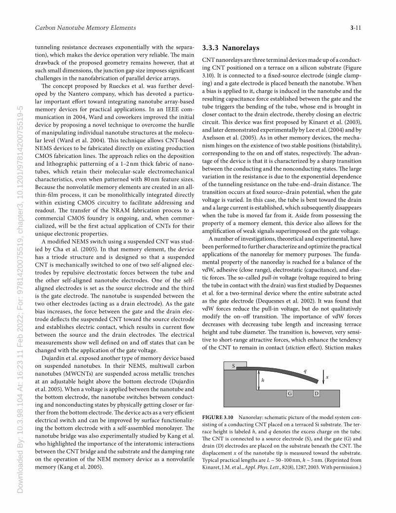
3.3.3 Nanorelays
CNT nanorelays are three terminal devices made up of a conduct-ing CNT positioned on a terrace on a silicon substrate (Figure 3.10). It is connected to a fixed-source electrode (single clamp-ing) and a gate electrode is placed beneath the nanotube. When a bias is applied to it, charge is induced in the nanotube and the resulting capacitance force established between the gate and the tube triggers the bending of the tube, whose end is brought in closer contact to the drain electrode, thereby closing an electric circuit. This device was first proposed by Kinaret et al. (2003), and later demonstrated experimentally by Lee et al. (2004) and by Axelsson et al. (2005). As in other memory devices, the mecha-nism hinges on the existence of two stable positions (bistability), corresponding to the on and off states, respectively. The advan-tage of the device is that it is characterized by a sharp transition between the conducting and the nonconducting states. The large variation in the resistance is due to the exponential dependence of the tunneling resistance on the tube-end–drain distance. The transition occurs at fixed source–drain potential, when the gate voltage is varied. In this case, the tube is bent toward the drain and a large current is established, which subsequently disappears when the tube is moved far from it. Aside from possessing the property of a memory element, this device also allows for the amplification of weak signals superimposed on the gate voltage.
A number of investigations, theoretical and experimental, have been performed to further characterize and optimize the practical applications of the nanorelay for memory purposes. The funda-mental property of the nanorelay is reached for a balance of the vdW, adhesive (close range), electrostatic (capacitance), and elas-tic forces. The so-called pull-in voltage (voltage required to bring the tube in contact with the drain) was first studied by Dequesnes et al. for a two-terminal device where the entire substrate acted as the gate electrode (Dequesnes et al. 2002). It was found that vdW forces reduce the pull-in voltage, but do not qualitatively modify the on–off transition. The importance of vdW forces decreases with decreasing tube length and increasing terrace height and tube diameter. The transition is, however, very sensi-tive to short-range attractive forces, which enhance the tendency of the CNT to remain in contact (stiction effect). Stiction makes
S
G D
h
qx
FIGURE 3.10 Nanorelay: schematic picture of the model system con-sisting of a conducting CNT placed on a terraced Si substrate. The ter-race height is labeled h, and q denotes the excess charge on the tube. The CNT is connected to a source electrode (S), and the gate (G) and drain (D) electrodes are placed on the substrate beneath the CNT. The displacement x of the nanotube tip is measured toward the substrate. Typical practical lengths are L ~ 50–100 nm, h ~ 5 nm. (Reprinted from Kinaret, J.M. et al., Appl. Phys. Lett., 82(8), 1287, 2003. With permission.)

Dow
nloa
ded
By:
10.
3.98
.104
At:
16:2
3 11
Feb
202
2; F
or: 9
7814
2007
5519
, cha
pter
3, 1
0.12
01/9
7814
2007
5519
-53-12 HandbookofNanophysics:NanoelectronicsandNanophotonics
the device unusable as it remains stuck in the on position (Jonsson et al. 2004a,b). The effect of the surface forces can be visualized by means of a stability diagram, which reveals the existence and positions of zero net force (local minima) on the cantilever as a function of gate voltage and tube deflection. A typical curve was computed by Jonsson et al. and is reproduced in Figure 3.11. A sta-bility diagram with more than one local equilibrium for a specific voltage results in a hysteretic behavior in the I–Vg characteristics (more than one position of zero net force means that there actu-ally are three such positions, one of which is not stable). The net force is positive to the right of the curve and negative to the left of the curve, so that, when lowering the voltage for a tube in contact with the drain electrode, it will not release until there is no stable position at the surface. The surface forces exacerbate this effect. The stiction problem corresponds to a stable nanotube position at the surface that can no longer be modified by the application of a gate voltage. The stiction problem is a general issue encountered in many nanotube-based devices. The problem of stiction hin-ders the use of SWNTs (because they are too flexible) as a bistable NEMS switch. MWNT and SWNT bundles are better candidates for bistable switching (Yousif et al. 2008). This problem can be alleviated, for example, by using stiffer (by avoiding total collapse
of the tube, e.g., by using MWCNTs) or shorter tubes. It can also be avoided by applying a layer of adsorbates.
Fujita et al. suggested a very different approach with a modi-fied device design. They proposed using a floating gate that is built between a bundle of CNTs and electrically isolated from the input and output electrodes. The bundle of CNTs is, therefore, bent by the electrostatic force between the floating and control gate, thereby allowing the on–off threshold voltage to be controlled by changing the back-gate voltage, similar to silicon MOSFET (Fujita et al. 2007). A consequence of reducing the possibility of stiction is that a higher pull-in voltage is required, and field emission from the end of the tip can be important. Field emission will become important when the effective potential at the tube end is equal or larger to the work function of the nanotube (i.e., about 4.5 V). For a set of design parameters, field emission can be deliberately sought after (noncontact mode). In the contact mode described above, tunneling current passes from the tube to the drain elec-trode. In the noncontact mode, the device is designed (short tube) in such a way that the tube is never in physical contact with the drain electrodes. In that case, an electron flow is established via a field emission mechanism. The field emission current onsets with a sufficiently large source–drain voltage and then increases nonlinearly as the source–drain voltage (i.e., the applied field) is further increased. The nanotube can be switched very quickly between the on and off states, and the nanorelay operation was evaluated to work in the gigahertz regime (Jonsson et al. 2004a).
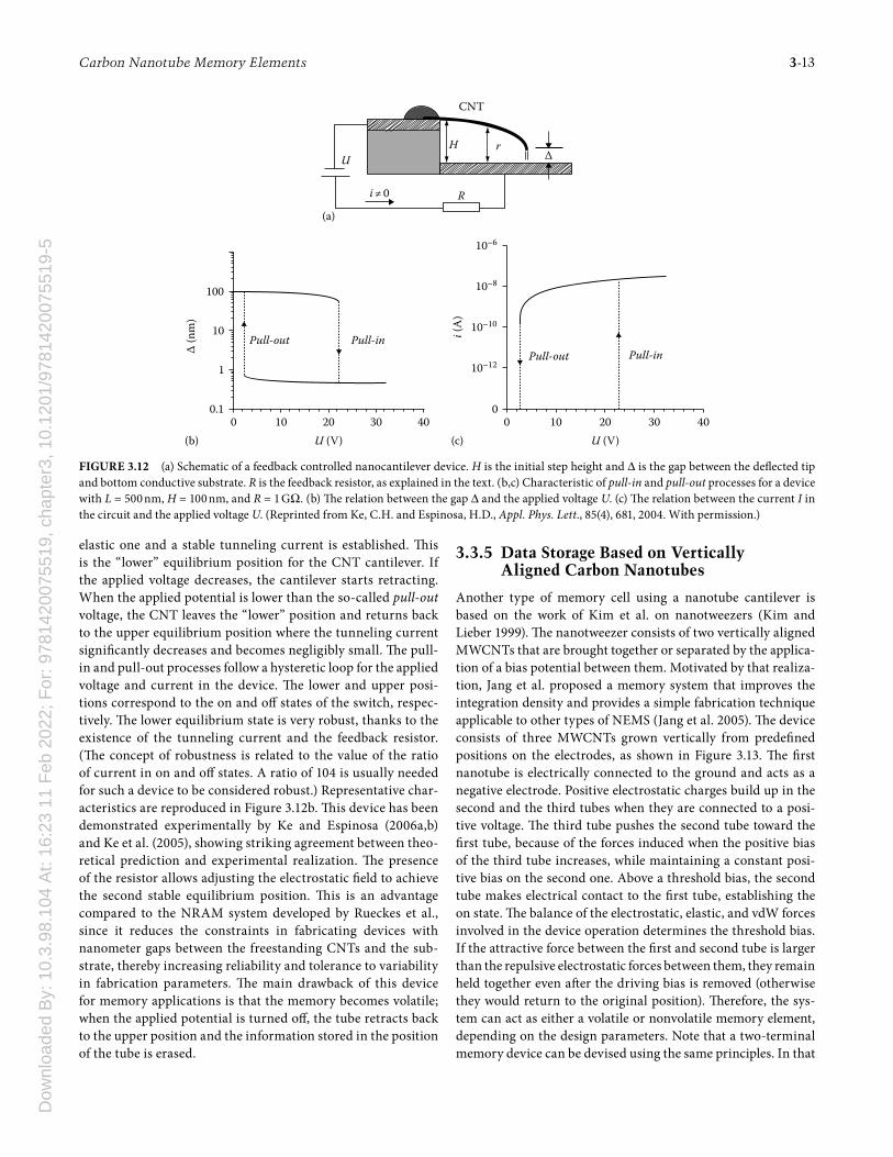
3.3.4 Feedback-Controlled Nanocantilevers
A variation of the nanorelay device presented in the previous section was proposed (Ke and Espinosa 2004), as shown in Figure 3.12a. It is made of an MWCNT placed as a cantilever over a micro-fabricated step. A bottom electrode, a resistor, and a power supply complete the device circuit. Compared to the nanorelay, this is a two-terminal device, providing more flex-ibility in terms of device realization and control. When the applied potential difference between the tube and the bottom electrode exceeds a certain potential, the tube becomes unsta-ble and collapses onto the electrode. The potential that causes the tube to collapse is defined as the pull-in voltage, already encountered above (Dequesnes et al. 2002). Above the pull-in voltage, the electrostatic force becomes larger than the elastic forces and the CNT accelerates toward the electrode. At small nanotube-tip electrode distance (of the order of 0.3–1.0 nm), substantial tunneling current passes between the tip of the tube and the bottom electrode. The main difference with the nanore-lay design is the presence of a resistance R placed in the circuit; with the increase in the current, the voltage drop at R increases, which causes a decrease in the effective tube-electrode poten-tial and the tube moves away from the electrode. It follows that the current decreases and a new equilibrium is reached. Without damping in the system, the cantilever would keep on oscillating at high frequency. However, damping is usually present, and the kinetic energy of the CNT dissipates. The tip ends up at a position where the electrostatic force is equal to the
00 1 2 3
Vg (V)
x (h
)
4 5 6 7
0.2
0.4
0.6
0.8
1B
With surfaceforces
Without surfaceforces
C A
FIGURE 3.11 Nanorelay stability diagram with and without surface forces computed with parameters given in Jonsson et al. (2004b). The curve shows the positions of zero net force on the tube (or local min-ima) as functions of gate voltage (at constant source voltage = 0.01 V) and deflection x (in units of h, see Figure 3.10). The large arrows show the direction of the force on each side of the curves, indicating that one local equilibrium state is unstable. The required voltage for pulling the tube to the surface (pull-in voltage) is given by A (~6.73 V). A tube at the surface will not leave the surface until the voltage is lower than the “release voltage,” B and C in the figure. Note that A > B, C, which indicates a hysteretic behavior in the current-gate voltage character-istics, a feature significantly enhanced by surface forces. (Reprinted from Jonsson, L.M. et al., Nanotechnology, 15(11), 1497, 2004a. With permission.)
Dow
nloa
ded
By:
10.
3.98
.104
At:
16:2
3 11
Feb
202
2; F
or: 9
7814
2007
5519
, cha
pter
3, 1
0.12
01/9
7814
2007
5519
-5CarbonNanotubeMemoryElements 3-13
elastic one and a stable tunneling current is established. This is the “lower” equilibrium position for the CNT cantilever. If the applied voltage decreases, the cantilever starts retracting. When the applied potential is lower than the so-called pull-out voltage, the CNT leaves the “lower” position and returns back to the upper equilibrium position where the tunneling current significantly decreases and becomes negligibly small. The pull-in and pull-out processes follow a hysteretic loop for the applied voltage and current in the device. The lower and upper posi-tions correspond to the on and off states of the switch, respec-tively. The lower equilibrium state is very robust, thanks to the existence of the tunneling current and the feedback resistor. (The concept of robustness is related to the value of the ratio of current in on and off states. A ratio of 104 is usually needed for such a device to be considered robust.) Representative char-acteristics are reproduced in Figure 3.12b. This device has been demonstrated experimentally by Ke and Espinosa (2006a,b) and Ke et al. (2005), showing striking agreement between theo-retical prediction and experimental realization. The presence of the resistor allows adjusting the electrostatic field to achieve the second stable equilibrium position. This is an advantage compared to the NRAM system developed by Rueckes et al., since it reduces the constraints in fabricating devices with nanometer gaps between the freestanding CNTs and the sub-strate, thereby increasing reliability and tolerance to variability in fabrication parameters. The main drawback of this device for memory applications is that the memory becomes volatile; when the applied potential is turned off, the tube retracts back to the upper position and the information stored in the position of the tube is erased.
3.3.5 Data Storage Based on Vertically aligned Carbon Nanotubes
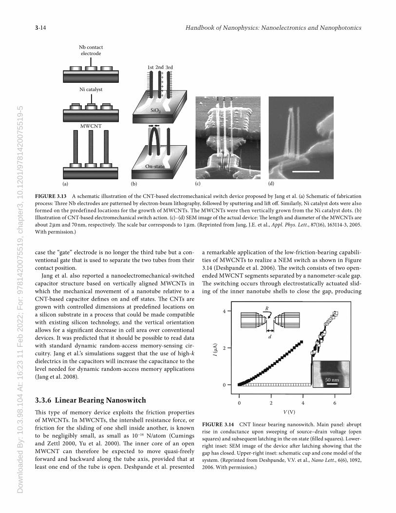
Another type of memory cell using a nanotube cantilever is based on the work of Kim et al. on nanotweezers (Kim and Lieber 1999). The nanotweezer consists of two vertically aligned MWCNTs that are brought together or separated by the applica-tion of a bias potential between them. Motivated by that realiza-tion, Jang et al. proposed a memory system that improves the integration density and provides a simple fabrication technique applicable to other types of NEMS (Jang et al. 2005). The device consists of three MWCNTs grown vertically from predefined positions on the electrodes, as shown in Figure 3.13. The first nanotube is electrically connected to the ground and acts as a negative electrode. Positive electrostatic charges build up in the second and the third tubes when they are connected to a posi-tive voltage. The third tube pushes the second tube toward the first tube, because of the forces induced when the positive bias of the third tube increases, while maintaining a constant posi-tive bias on the second one. Above a threshold bias, the second tube makes electrical contact to the first tube, establishing the on state. The balance of the electrostatic, elastic, and vdW forces involved in the device operation determines the threshold bias. If the attractive force between the first and second tube is larger than the repulsive electrostatic forces between them, they remain held together even after the driving bias is removed (otherwise they would return to the original position). Therefore, the sys-tem can act as either a volatile or nonvolatile memory element, depending on the design parameters. Note that a two-terminal memory device can be devised using the same principles. In that
(c)(b)
100
10Pull-out
Pull-outPull-in
Pull-in1
0.1 0
10–12
10–10
i (A
)
10–8
10–6
0 10 20U (V)
Δ (n
m)
30 40 0 10 20U (V)
30 40
(a)
U
R
H rΔ
CNT
i ≠ 0
FIGURE 3.12 (a) Schematic of a feedback controlled nanocantilever device. H is the initial step height and Δ is the gap between the deflected tip and bottom conductive substrate. R is the feedback resistor, as explained in the text. (b,c) Characteristic of pull-in and pull-out processes for a device with L = 500 nm, H = 100 nm, and R = 1 GΩ. (b) The relation between the gap Δ and the applied voltage U. (c) The relation between the current I in the circuit and the applied voltage U. (Reprinted from Ke, C.H. and Espinosa, H.D., Appl. Phys. Lett., 85(4), 681, 2004. With permission.)
Dow
nloa
ded
By:
10.
3.98
.104
At:
16:2
3 11
Feb
202
2; F
or: 9
7814
2007
5519
, cha
pter
3, 1
0.12
01/9
7814
2007
5519
-53-14 HandbookofNanophysics:NanoelectronicsandNanophotonics
case the “gate” electrode is no longer the third tube but a con-ventional gate that is used to separate the two tubes from their contact position.
Jang et al. also reported a nanoelectromechanical-switched capacitor structure based on vertically aligned MWCNTs in which the mechanical movement of a nanotube relative to a CNT-based capacitor defines on and off states. The CNTs are grown with controlled dimensions at predefined locations on a silicon substrate in a process that could be made compatible with existing silicon technology, and the vertical orientation allows for a significant decrease in cell area over conventional devices. It was predicted that it should be possible to read data with standard dynamic random-access memory-sensing cir-cuitry. Jang et al.’s simulations suggest that the use of high-k dielectrics in the capacitors will increase the capacitance to the level needed for dynamic random-access memory applications (Jang et al. 2008).
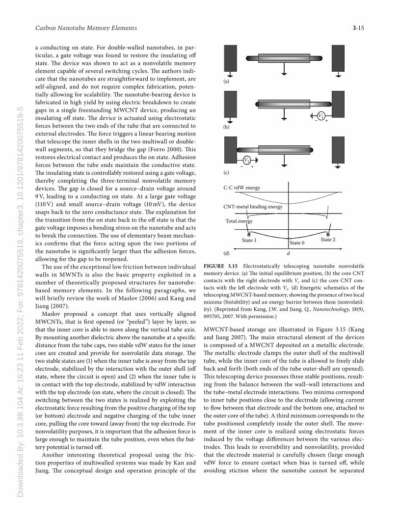
3.3.6 Linear Bearing Nanoswitch
This type of memory device exploits the friction properties of MWCNTs. In MWCNTs, the intershell resistance force, or friction for the sliding of one shell inside another, is known to be negligibly small, as small as 10−14 N/atom (Cumings and Zettl 2000, Yu et al. 2000). The inner core of an open MWCNT can therefore be expected to move quasi-freely forward and backward along the tube axis, provided that at least one end of the tube is open. Deshpande et al. presented
a remarkable application of the low-friction-bearing capabili-ties of MWCNTs to realize a NEM switch as shown in Figure 3.14 (Deshpande et al. 2006). The switch consists of two open-ended MWCNT segments separated by a nanometer-scale gap. The switching occurs through electrostatically actuated slid-ing of the inner nanotube shells to close the gap, producing
4
2
0
0 2 4 6
V (V)
50 nm
I (μA
)
R
d
FIGURE 3.14 CNT linear bearing nanoswitch. Main panel: abrupt rise in conductance upon sweeping of source–drain voltage (open squares) and subsequent latching in the on state (filled squares). Lower-right inset: SEM image of the device after latching showing that the gap has closed. Upper-right inset: schematic cup and cone model of the system. (Reprinted from Deshpande, V.V. et al., Nano Lett., 6(6), 1092, 2006. With permission.)
(a)
1 2 3
Nb contactelectrode
Ni catalyst
MWCNT
1st
SiO2
On-state
2nd 3rd+––––––––––––––
+++++++++++++
++++
(b) (c) (d)
FIGURE 3.13 A schematic illustration of the CNT-based electromechanical switch device proposed by Jang et al. (a) Schematic of fabrication process: Three Nb electrodes are patterned by electron-beam lithography, followed by sputtering and lift off. Similarly, Ni catalyst dots were also formed on the predefined locations for the growth of MWCNTs. The MWCNTs were then vertically grown from the Ni catalyst dots. (b) Illustration of CNT-based electromechanical switch action. (c)–(d) SEM image of the actual device: The length and diameter of the MWCNTs are about 2 μm and 70 nm, respectively. The scale bar corresponds to 1 μm. (Reprinted from Jang, J.E. et al., Appl. Phys. Lett., 87(16), 163114-3, 2005. With permission.)
Dow
nloa
ded
By:
10.
3.98
.104
At:
16:2
3 11
Feb
202
2; F
or: 9
7814
2007
5519
, cha
pter
3, 1
0.12
01/9
7814
2007
5519
-5CarbonNanotubeMemoryElements 3-15
a conducting on state. For double-walled nanotubes, in par-ticular, a gate voltage was found to restore the insulating off state. The device was shown to act as a nonvolatile memory element capable of several switching cycles. The authors indi-cate that the nanotubes are straightforward to implement, are self-aligned, and do not require complex fabrication, poten-tially allowing for scalability. The nanotube-bearing device is fabricated in high yield by using electric breakdown to create gaps in a single freestanding MWCNT device, producing an insulating off state. The device is actuated using electrostatic forces between the two ends of the tube that are connected to external electrodes. The force triggers a linear bearing motion that telescope the inner shells in the two multiwall or double-wall segments, so that they bridge the gap (Forro 2000). This restores electrical contact and produces the on state. Adhesion forces between the tube ends maintain the conductive state. The insulating state is controllably restored using a gate voltage, thereby completing the three-terminal nonvolatile memory devices. The gap is closed for a source–drain voltage around 9 V, leading to a conducting on state. At a large gate voltage (110 V) and small source–drain voltage (10 mV), the device snaps back to the zero conductance state. The explanation for the transition from the on state back to the off state is that the gate voltage imposes a bending stress on the nanotube and acts to break the connection. The use of elementary beam mechan-ics confirms that the force acting upon the two portions of the nanotube is significantly larger than the adhesion forces, allowing for the gap to be reopened.
The use of the exceptional low friction between individual walls in MWNTs is also the basic property exploited in a number of theoretically proposed structures for nanotube-based memory elements. In the following paragraphs, we will brief ly review the work of Maslov (2006) and Kang and Jiang (2007).
Maslov proposed a concept that uses vertically aligned MWCNTs, that is first opened (or “peeled”) layer by layer, so that the inner core is able to move along the vertical tube axis. By mounting another dielectric above the nanotube at a specific distance from the tube caps, two stable vdW states for the inner core are created and provide for nonvolatile data storage. The two stable states are (1) when the inner tube is away from the top electrode, stabilized by the interaction with the outer shell (off state, where the circuit is open) and (2) when the inner tube is in contact with the top electrode, stabilized by vdW interaction with the top electrode (on state, where the circuit is closed). The switching between the two states is realized by exploiting the electrostatic force resulting from the positive charging of the top (or bottom) electrode and negative charging of the tube inner core, pulling the core toward (away from) the top electrode. For nonvolatility purposes, it is important that the adhesion force is large enough to maintain the tube position, even when the bat-tery potential is turned off.
Another interesting theoretical proposal using the fric-tion properties of multiwalled systems was made by Kan and Jiang. The conceptual design and operation principle of the
MWCNT-based storage are illustrated in Figure 3.15 (Kang and Jiang 2007). The main structural element of the devices is composed of a MWCNT deposited on a metallic electrode. The metallic electrode clamps the outer shell of the multiwall tube, while the inner core of the tube is allowed to freely slide back and forth (both ends of the tube outer-shell are opened). This telescoping device possesses three stable positions, result-ing from the balance between the wall–wall interactions and the tube–metal electrode interactions. Two minima correspond to inner tube positions close to the electrode (allowing current to flow between that electrode and the bottom one, attached to the outer core of the tube). A third minimum corresponds to the tube positioned completely inside the outer shell. The move-ment of the inner core is realized using electrostatic forces induced by the voltage differences between the various elec-trodes. This leads to reversibility and nonvolatility, provided that the electrode material is carefully chosen (large enough vdW force to ensure contact when bias is turned off, while avoiding stiction where the nanotube cannot be separated
(a)
(b)
(c)
V2
V1
–
–
+
+
C-C vdW energy
CNT-metal binding energy
Total energy
State 1 State 0 State 2
d(d)
FIGURE 3.15 Electrostatically telescoping nanotube nonvolatile memory device. (a) The initial equilibrium position, (b) the core CNT contacts with the right electrode with V1 and (c) the core CNT con-tacts with the left electrode with V2. (d) Energetic schematics of the telescoping MWCNT-based memory, showing the presence of two local minima (bistability) and an energy barrier between them (nonvolatil-ity). (Reprinted from Kang, J.W. and Jiang, Q., Nanotechnology, 18(9), 095705, 2007. With permission.)
Dow
nloa
ded
By:
10.
3.98
.104
At:
16:2
3 11
Feb
202
2; F
or: 9
7814
2007
5519
, cha
pter
3, 1
0.12
01/9
7814
2007
5519
-53-16 HandbookofNanophysics:NanoelectronicsandNanophotonics
from the electrode anymore due to small range forces, as illus-trated in Figure 3.15b).
3.3.7 Conclusions
In this section, we have presented the state of the art of fundamen-tal research of the use of CNTs NEMS for memory applications. The CNT-NEMS are particularly interesting because they exploit the two most remarkable properties of CNTs, namely, their elec-tronic and mechanical properties. The viability of CNT-based NEMS switches and their comparison with their CMOS equiva-lents was recently presented by Yousif et al. (2008). A detailed analysis of performance metrics regarding threshold voltage control, static and dynamic power dissipation, and speed and integration density revealed that apart from packaging and reli-ability issues (which are the subject of intense current research), nanotube-based switches are competitive in low power, particu-larly low-standby power, logic, and memory applications.
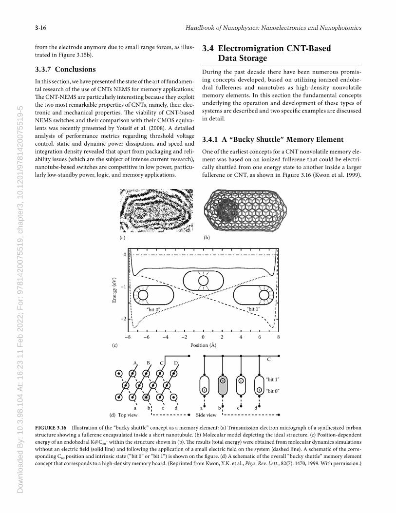
3.4 Electromigration CNt-Based Data Storage
During the past decade there have been numerous promis-ing concepts developed, based on utilizing ionized endohe-dral fullerenes and nanotubes as high-density nonvolatile memory elements. In this section the fundamental concepts underlying the operation and development of these types of systems are described and two specific examples are discussed in detail.
3.4.1 a “Bucky Shuttle” Memory Element
One of the earliest concepts for a CNT nonvolatile memory ele-ment was based on an ionized fullerene that could be electri-cally shuttled from one energy state to another inside a larger fullerene or CNT, as shown in Figure 3.16 (Kwon et al. 1999).
(a) (b)
(c)
0
–1
–2
–8 –6 –4
A
a ab bc c
C
dSide view
“bit 0”
“bit 1”
d
+
++
+
B C D
Top view
–2
“bit 0” “bit 1”
0Position (Å)
Ener
gy (e
V)
2 4 6 8
(d)
FIGURE 3.16 Illustration of the “bucky shuttle” concept as a memory element: (a) Transmission electron micrograph of a synthesized carbon structure showing a fullerene encapsulated inside a short nanotubule. (b) Molecular model depicting the ideal structure. (c) Position-dependent energy of an endohedral K@C60
+ within the structure shown in (b). The results (total energy) were obtained from molecular dynamics simulations without an electric field (solid line) and following the application of a small electric field on the system (dashed line). A schematic of the corre-sponding C60 position and intrinsic state (“bit 0” or “bit 1”) is shown on the figure. (d) A schematic of the overall “bucky shuttle” memory element concept that corresponds to a high-density memory board. (Reprinted from Kwon, Y.K. et al., Phys. Rev. Lett., 82(7), 1470, 1999. With permission.)
Dow
nloa
ded
By:
10.
3.98
.104
At:
16:2
3 11
Feb
202
2; F
or: 9
7814
2007
5519
, cha
pter
3, 1
0.12
01/9
7814
2007
5519
-5CarbonNanotubeMemoryElements 3-17
One advantage of this concept was an appropriate material could be self-assembled from elemental carbon via thermal treatment of diamond power. A unique geometry of a nano-tube encapsulating a fullerene, where a small fullerene struc-ture could reside at one of the two ends of a capped nanotube or larger fullerene was experimentally identified (Figure 3.16a), and this structural arrangement became the basis for the original concept of a “bucky shuttle” memory element. In this system the on (bit 1) and off (bit 0) states correspond to the two ends of the nanotube that are local minima in the energy landscape of the endohedral fullerene (Figure 3.16c). The position of the ionized endohedral fullerene (obtained by doping with potassium, e.g., K+@C60) can be manipulated by applying a bias voltage across the ends of the nanotube. The energetics of a switching field of 0.1 V/Å generated by apply-ing a voltage of 1.5 V is shown in Figure 3.16c. With such a small electric field, integrity problems are not expected since graphitic structures are known not to degrade under fields of <3 V/Å. The overall thermal stability and nonvolatility of the system directly depends on the relative depth of the energy minima for the two states. Molecular dynamics simulations were used to explore the functional operation regime for the “bucky shuttle” and also to perform detailed performance analyses. Those calculations successfully demonstrated that information stored would be thermally stable well beyond room temperature, requiring temperatures above 3000 K to be destroyed. In addition, the results indicated that the “bucky shuttle” can be switched between the two states on a very fast timescale, ∼10 ps, by applying a small electric field. This opera-tion regime would allow for memory-switching access of close to 0.1 THz, giving a data throughput rate of 10 Gbyte/s in its simplest serial mode. Parallel arrays of the “bucky shuttles” could be envisioned from ordered close-packed nanotube arrays and such an assembly could potentially provide unprec-edented memory storage (Figure 3.16d). This ideal system would offer a nonvolatile memory device with a combination of high switching speed and high density.
3.4.2 Memory Elements Based on the “Bucky Shuttle” Concept
While the “bucky shuttle” concept provides a relatively simple mechanism for storing information at the nanoscale, and it is strongly supported by molecular dynamics simulations that have solidified its theoretical operation, a practical measure-ment of the intrinsic on and off states is not clear. Also, the experimental production, although shown possible using self-assembly, is not able to exclusively produce the required “bucky shuttle” structures and would require novel separation and sorting techniques to facilitate their practical use. These short-comings stimulated the development of a number of related concepts that have continued to evolve, such as a “nanotube shuttle” employing a transition from single-walled to double-walled nanotube for detection of the “shuttle” position (Kang
and Hwang 2004c, 2005a), multi-endo-fullerenes- or peapod-based shuttles (Kang and Hwang 2004c, 2005b), and variations of these including boron nitride nanotubes (Choi et al. 2004, Hwang et al. 2005b), bipolar endo-fullerenes (Hwang et al. 2005a), metallofullerenes (Byun et al. 2004), and ionic fluidic media (Kang and Hwang 2004b). Again, the basic underly-ing concept relies on the electromigration of an encapsulated architecture(s) from one local energy minimum to another. The “nanotube shuttle,” for example (see Figure 3.17), is based on the use of a capped peapod (nanotube with multiple endo-hedral C60s, see Figure 3.17a), which is subjected to thermal and e-beam treatment (Figure 3.17b) that subsequently causes coalescence of the encapsulated C60s to form an inner tubule. This is a well-known experimental process and one of the pri-mary methods used for producing high-quality double-walled CNTs. The capped double-walled carbon nanotube (DWCNT) is then cut using lithography and etching technology in order to produce two aligned open ends with the inner tubule ini-tially residing within one end (Figure 3.17c through e). The shuttle mechanism allows the inner tubule to move from one tube end across the gap into the other tube (Figure 3.17f). The separation of the two open ends is required in order to have two independent nanotube structures, which is critical for detect-ing the state that the overall system is in. The separation must be large enough to preempt strong interactions between the two nanotube structures (the two ends need to be independent in order for the electronic structure to allow unique detection) but small enough so as to prevent the shuttling inner tubule from completely escaping. For such an ideal system, the position of the inner tubule could in principle be measured by detecting the electronic structure of one of the ends since it will change from that corresponding to a single-walled to a double-walled nanotube (Lee et al. 2002).
3.4.3 Conclusions
The general “bucky shuttle” concept relies on utilizing the basic principle of electromigration in a two-level system defined by an ionized encapsulated fullerene-based structure. Its operation has been demonstrated to be very efficient (very short switch-ing times) and is in general highly robust in regard to thermal and electrical stability. In addition, the possibility of assembling very high density architectures promises to allow construction of memory elements with high switching speed, high density, and nonvolatile storage of data. Unfortunately, despite the tre-mendous interest in the fundamentally simple and attractive systems underlying the use of CNT-based electromigration for memory elements, experimental realization has been difficult. This is because of the complexities in practical fabrication of the required structures and for making appropriate electrical con-tacts with them. As such, these types of systems have remained as conceptual ideas, to date, relying on the proof-of-principles results primarily obtained from classical molecular dynamics simulations.
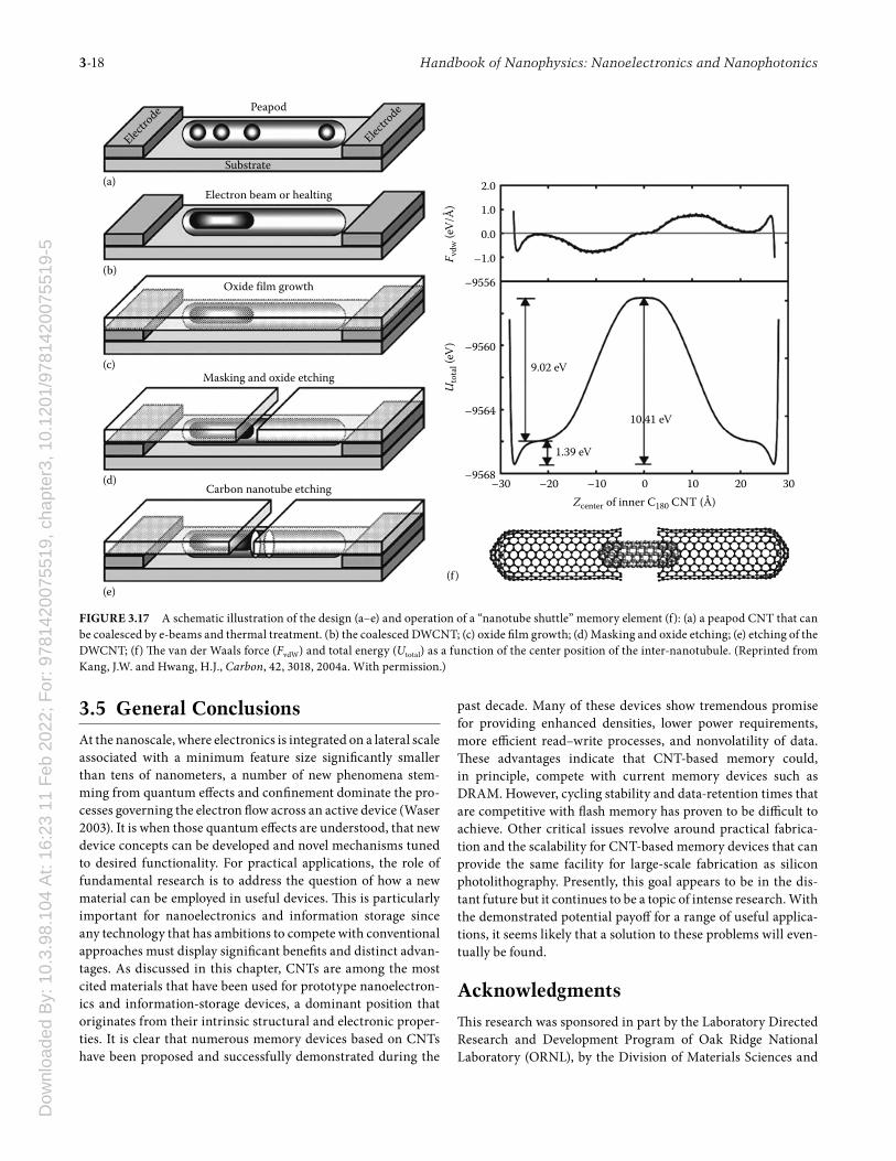
Dow
nloa
ded
By:
10.
3.98
.104
At:
16:2
3 11
Feb
202
2; F
or: 9
7814
2007
5519
, cha
pter
3, 1
0.12
01/9
7814
2007
5519
-53-18 HandbookofNanophysics:NanoelectronicsandNanophotonics
3.5 General Conclusions
At the nanoscale, where electronics is integrated on a lateral scale associated with a minimum feature size significantly smaller than tens of nanometers, a number of new phenomena stem-ming from quantum effects and confinement dominate the pro-cesses governing the electron flow across an active device (Waser 2003). It is when those quantum effects are understood, that new device concepts can be developed and novel mechanisms tuned to desired functionality. For practical applications, the role of fundamental research is to address the question of how a new material can be employed in useful devices. This is particularly important for nanoelectronics and information storage since any technology that has ambitions to compete with conventional approaches must display significant benefits and distinct advan-tages. As discussed in this chapter, CNTs are among the most cited materials that have been used for prototype nanoelectron-ics and information-storage devices, a dominant position that originates from their intrinsic structural and electronic proper-ties. It is clear that numerous memory devices based on CNTs have been proposed and successfully demonstrated during the
past decade. Many of these devices show tremendous promise for providing enhanced densities, lower power requirements, more efficient read–write processes, and nonvolatility of data. These advantages indicate that CNT-based memory could, in principle, compete with current memory devices such as DRAM. However, cycling stability and data-retention times that are competitive with flash memory has proven to be difficult to achieve. Other critical issues revolve around practical fabrica-tion and the scalability for CNT-based memory devices that can provide the same facility for large-scale fabrication as silicon photolithography. Presently, this goal appears to be in the dis-tant future but it continues to be a topic of intense research. With the demonstrated potential payoff for a range of useful applica-tions, it seems likely that a solution to these problems will even-tually be found.
acknowledgments
This research was sponsored in part by the Laboratory Directed Research and Development Program of Oak Ridge National Laboratory (ORNL), by the Division of Materials Sciences and
(f )
(a)
Peapod
Substrate
Electron beam or healting
Oxide film growth
Masking and oxide etching
Carbon nanotube etching
2.0
1.0
0.0
–1.0
–9556
F vdw
(eV/
Å)
Uto
tal (
eV) –9560
9.02 eV
1.39 eV
10.41 eV–9564
–9568–30 –20 –10 0
Zcenter of inner C180 CNT (Å)10 20 30
Electro
de
Electro
de
(b)
(c)
(d)
(e)
FIGURE 3.17 A schematic illustration of the design (a–e) and operation of a “nanotube shuttle” memory element (f): (a) a peapod CNT that can be coalesced by e-beams and thermal treatment. (b) the coalesced DWCNT; (c) oxide film growth; (d) Masking and oxide etching; (e) etching of the DWCNT; (f) The van der Waals force (FvdW) and total energy (Utotal) as a function of the center position of the inter-nanotubule. (Reprinted from Kang, J.W. and Hwang, H.J., Carbon, 42, 3018, 2004a. With permission.)
Dow
nloa
ded
By:
10.
3.98
.104
At:
16:2
3 11
Feb
202
2; F
or: 9
7814
2007
5519
, cha
pter
3, 1
0.12
01/9
7814
2007
5519
-5CarbonNanotubeMemoryElements 3-19
Engineering, and by the Center of Nanophase Materials Science, U.S. Department of Energy under Contract No. DEAC05-00OR22725 with UT-Battelle, LLC at ORNL.
references
Akdim, B. and Pachter, R., Switching behavior in pi-conjugated molecules bridging nonmetallic electrodes: A density func-tional theory study, Journal of Physical Chemistry C 112(9), 3170–3174, 2008.
Axelsson, S., Campbell, E. E. B., Jonsson, L. M. et al., Theoretical and experimental investigations of three-terminal carbon nanotube relays, New Journal of Physics 7, 245, 2005.
Bachhofer, H., Reisinger, H., Bertagnolli, E., and von Philipsborn, H., Transient conduction in multidielectric silicon-oxide-nitride-oxide semiconductor structures, Journal of Applied Physics 89(5), 2791–2800, 2001.
Bernholc, J., Brenner, D., Nardelli, M. B., Meunier, V., and Roland, C., Mechanical and electrical properties of nanotubes, Annual Review of Materials Research 32, 347–375, 2002.
Bichoutskaia, E., Popov, A. M., and Lozovik, Y. E., Nanotube-based data storage devices, Materials Today 11(6), 38–43, 2008.
Byun, K. R., Kang, J. W., and Hwang, H. J., Nanoscale data storage device of metallofullerene peapods, Journal of the Korean Physical Society 45(2), 416–422, 2004.
Cha, S. N., Jang, J. E., Choi, Y. et al., Fabrication of a nanoelec-tromechanical switch using a suspended carbon nanotube, Applied Physics Letters 86(8), 083105-3, 2005.
Chakraborty, R. S., Narasimhan, S., and Bhunia, S., Hybridization of CMOS with CNT-based nano-electromechanical switch for low leakage and robust circuit design, IEEE Transactions on Circuits and Systems I—Regular Papers 54(11), 2480–2488, 2007.
Chakraborty, G., Sarkar, C. K., Lu, X. B., and Dai, J. Y., Study of the tunnelling initiated leakage current through the carbon nanotube embedded gate oxide in metal oxide semiconduc-tor structures, Nanotechnology 19(25), 255401, 2008.
Charlier, J. C., Blase, X., and Roche, S., Electronic and transport properties of nanotubes, Reviews of Modern Physics 79(2), 677–732, 2007.
Choi, W. B., Chae, S., Bae, E. et al., Carbon-nanotube-based nonvolatile memory with oxide-nitride-oxide film and nanoscale channel, Applied Physics Letters 82(2), 275–277, 2003.
Choi, W. Y., Kang, J. W., and Hwang, H. J., Bucky shuttle mem-ory system based on boron-nitride nanopeapod, Physica E—Low-Dimensional Systems & Nanostructures 23(1–2), 135–140, 2004.
Cui, J. B., Sordan, R., Burghard, M., and Kern, K., Carbon nano-tube memory devices of high charge storage stability, Applied Physics Letters 81(17), 3260–3262, 2002.
Cumings, J. and Zettl, A., Low-friction nanoscale linear bear-ing realized from multiwall carbon nanotubes, Science 289(5479), 602–604, 2000.
Dequesnes, M., Rotkin, S. V., and Aluru, N. R., Calculation of pull-in voltages for carbon-nanotube-based nanoelectro-mechanical switches, Nanotechnology 13(1), 120–131, 2002.
Derycke, V., Martel, R., Appenzeller, J., and Avouris, P., Carbon nanotube inter- and intramolecular logic gates, Nano Letters 1(9), 453–456, 2001.
Derycke, V., Martel, R., Appenzeller, J., and Avouris, P., Controlling doping and carrier injection in carbon nanotube transis-tors, Applied Physics Letters 80(15), 2773–2775, 2002.
Deshpande, V. V., Chiu, H. Y., Postma, H. W. C. et al., Carbon nanotube linear bearing nanoswitches, Nano Letters 6(6), 1092–1095, 2006.
Duan, X. F., Huang, Y., and Lieber, C. M., Nonvolatile memory and programmable logic from molecule-gated nanowires, Nano Letters 2(5), 487–490, 2002.
Dujardin, E., Derycke, V., Goffman, M. F., Lefevre, R., and Bourgoin, J. P., Self-assembled switches based on electro-actuated multiwalled nanotubes, Applied Physics Letters 87(19), 193107-3, 2005.
Forro, L., Nanotechnology: Beyond Gedanken experiments, Science 289(5479), 560–561, 2000.
Freitag, M., Johnson, A. T., Kalinin, S. V., and Bonnell, D. A., Role of single defects in electronic transport through carbon nanotube field-effect transistors, Physical Review Letters 89(21), 216801, 2002.
Fuhrer, M. S., Kim, B. M., Durkop, T., and Brintlinger, T., High-mobility nanotube transistor memory, Nano Letters 2(7), 755–759, 2002.
Fujita, S., Nomura, K., Abe, K., and Lee, T. H., 3-d nanoarchi-tectures with carbon nanotube mechanical switches for future on-chip network beyond CMOS architecture, IEEE Transactions on Circuits and Systems I—Regular Papers 54(11), 2472–2479, 2007.
Ganguly, U., Kan, E. C., and Zhang, Y., Carbon nanotube-based nonvolatile memory with charge storage in metal nanocrys-tals, Applied Physics Letters 87(4), 043108-3, 2005.
Goldsmith, B. R., Coroneus, J. G., Khalap, V. R. et al., Conductance-controlled point functionalization of single-walled carbon nanotubes, Science 315(5808), 77–81, 2007.
He, J. L., Chen, B., Flatt, A. K. et al., Metal-free silicon-molecule-nanotube testbed and memory device, Nature Materials 5(1), 63–68, 2006.
Hwang, H. J., Byun, K. R., Lee, J. Y., and Kang, J. W., A nanoscale field effect data storage of bipolar endo-fullerenes shuttle device, Current Applied Physics 5(6), 609–614, 2005a.
Hwang, H. J., Choi, W. Y., and Kang, J. W., Molecular dynam-ics simulations of nanomemory element based on boron-nitride nanotube-to-peapod transition, Computational Materials Science 33(1–3), 317–324, 2005b.
Jang, J. E., Cha, S. N., Choi, Y. et al., Nanoelectromechanical switches with vertically aligned carbon nanotubes, Applied Physics Letters 87(16), 163114-3, 2005.
Jang, J. E., Cha, S. N., Choi, Y. J. et al., Nanoscale memory cell based on a nanoelectromechanical switched capacitor, Nature Nanotechnology 3(1), 26–30, 2008.
Dow
nloa
ded
By:
10.
3.98
.104
At:
16:2
3 11
Feb
202
2; F
or: 9
7814
2007
5519
, cha
pter
3, 1
0.12
01/9
7814
2007
5519
-53-20 HandbookofNanophysics:NanoelectronicsandNanophotonics
Jonsson, L. M., Axelsson, S., Nord, T., Viefers, S., and Kinaret, J. M., High frequency properties of a CNT-based nanorelay, Nanotechnology 15(11), 1497–1502, 2004a.
Jonsson, L. M., Nord, T., Kinaret, J. M., and Viefers, S., Effects of surface forces and phonon dissipation in a three-terminal nanorelay, Journal of Applied Physics 96(1), 629–635, 2004b.
Kang, J. W. and Hwang, H. J., Carbon nanotube shuttle’ memory device, Carbon 42, 3018–3021, 2004a.
Kang, J. W. and Hwang, H. J., Nano-memory-element applica-tions of carbon nanocapsule encapsulating potassium ions: Molecular dynamics study, Journal of the Korean Physical Society 44(4), 879–883, 2004b.
Kang, J. W. and Hwang, H. J., Schematics and atomistic simula-tions of nanomemory element based on carbon tube-to-peapod transition, Japanese Journal of Applied Physics Part 1—Regular Papers Short Notes & Review Papers 43(7A), 4447–4452, 2004c.
Kang, J. W. and Hwang, H. J., Carbon nanotube shuttle memory device based on singlewall-to-doublewall carbon nanotube transition, Computational Materials Science 33(1–3), 338–345, 2005a.
Kang, J. W. and Hwang, H. J., Schematics and simulations of nanomemory device based on nanopeapods, Materials Science & Engineering C—Biomimetic and Supramolecular Systems 25(5–8), 843–847, 2005b.
Kang, J. W. and Jiang, Q., Electrostatically telescoping nanotube nonvolatile memory device, Nanotechnology 18(9), 095705, 2007.
Kang, J. W., Lee, J. H., Lee, H. J., and Hwang, H. J., A study on car-bon nanotube bridge as a electromechanical memory device, Physica E: Low-Dimensional Systems and Nanostructures 27(3), 332–340, 2005.
Ke, C. H. and Espinosa, H. D., Feedback controlled nanocanti-lever device, Applied Physics Letters 85(4), 681–683, 2004.
Ke, C.-H. and Espinosa, H. D., Nanoelectromechanical sys-tems and modeling, in Handbook of Theoretical and Computational Nanotechnology American Scientific Publishers, Valencia, CA, 2006a.
Ke, C. H. and Espinosa, H. D., In situ electron microscopy elec-tromechanical characterization of a bistable NEMS device, Small 2(12), 1484–1489, 2006b.
Ke, C. H., Pugno, N., Peng, B., and Espinosa, H. D., Experiments and modeling of carbon nanotube-based NEMS devices, Journal of the Mechanics and Physics of Solids 53(6), 1314–1333, 2005.
Kim, P. and Lieber, C. M., Nanotube nanotweezers, Science 286(5447), 2148–2150, 1999.
Kim, W., Javey, A., Vermesh, O. et al., Hysteresis caused by water molecules in carbon nanotube field-effect transistors, Nano Letters 3(2), 193–198, 2003.
Kinaret, J. M., Nord, T., and Viefers, S., A carbon-nanotube-based nanorelay, Applied Physics Letters 82(8), 1287–1289, 2003.
Kwon, Y. K., Tomanek, D., and Iijima, S., “Bucky shuttle” memory device: Synthetic approach and molecular dynamics simu-lations, Physical Review Letters 82(7), 1470–1473, 1999.
Lee, J., Kim, H., Kahng, S.-J. et al., Bandgap modulation of carbon nanotubes by encapsulated metallofullerenes, Nature 415, 1005–1008, 2002.
Lee, S. W., Lee, D. S., Morjan, R. E. et al., A three-terminal carbon nanorelay, Nano Letters 4(10), 2027–2030, 2004.
Lu, X. B. and Dai, J. Y., Memory effects of carbon nanotubes as charge storage nodes for floating gate memory applications, Applied Physics Letters 88(11), 113104-3, 2006.
Mannik, J., Goldsmith, B. R., Kane, A., and Collins, P. G., Chemically induced conductance switching in carbon nanotube circuits, Physical Review Letters 97(1), 016601, 2006.
Martel, R., Schmidt, T., Shea, H. R., Hertel, T., and Avouris, P., Single- and multi-wall carbon nanotube field-effect transis-tors, Applied Physics Letters 73(17), 2447–2449, 1998.
Martel, R., Derycke, V., Lavoie, C. et al., Ambipolar electrical transport in semiconducting single-wall carbon nanotubes, Physical Review Letters 87(25), 256805, 2001.
Maslov, L., Concept of nonvolatile memory based on multiwall carbon nanotubes, Nanotechnology 17(10), 2475–2482, 2006.
Meunier, V. and Sumpter, B. G., Tuning the conductance of carbon nanotubes with encapsulated molecules, Nanotechnology 18(42), 424032, 2007.
Meunier, V., Kalinin, S. V., Shin, J., Baddorf, A. P., and Harrison, R. J., Quantitative analysis of electronic properties of carbon nanotubes by scanning probe microscopy: From atomic to mesoscopic length scales, Physical Review Letters 93(24), 246801, 2004.
Meunier, V., Kalinin, S. V., and Sumpter, B. G., Nonvolatile memory elements based on the intercalation of organic molecules inside carbon nanotubes, Physical Review Letters 98(5), 056401, 2007.
Radosavljevic, M., Freitag, M., Thadani, K. V., and Johnson, A. T., Nonvolatile molecular memory elements based on ambi-polar nanotube field effect transistors, Nano Letters 2(7), 761–764, 2002.
Rueckes, T., Kim, K., Joselevich, E. et al., Carbon nanotube-based nonvolatile random access memory for molecular comput-ing, Science 289(5476), 94–97, 2000.
Sakurai, T., Yoshimura, T., Akita, S., Fujimura, N., and Nakayama, Y., Single-wall carbon nanotube field effect transistors with non-volatile memory operation, Japanese Journal of Applied Physics Part 2—Letters & Express Letters 45(37–41), L1036–L1038, 2006.
Scott, J. C., Materials science: Is there an immortal memory? Science 304(5667), 62–63, 2004.
Star, A., Lu, Y., Bradley, K., and Gruner, G., Nanotube optoelec-tronic memory devices, Nano Letters 4(9), 1587–1591, 2004.
Tans, S. J., Verschueren, A. R. M., and Dekker, C., Room-temperature transistor based on a single carbon nanotube, Nature 393(6680), 49–52, 1998.
Ward, J. W., Meinhold, M., Segal, B. M. et al., A nonvolatile nanoelectromechanical memory element utilizing a fabric of carbon nanotubes, in Non-Volatile Memory Technology Symposium, Orlando, FL, 2004, pp. 34–38.
Dow
nloa
ded
By:
10.
3.98
.104
At:
16:2
3 11
Feb
202
2; F
or: 9
7814
2007
5519
, cha
pter
3, 1
0.12
01/9
7814
2007
5519
-5CarbonNanotubeMemoryElements 3-21
Waser, R., Nanoelectronics and Information Technology: Advanced Electronic Materials and Novel Devices, Wiley-VCH, Weinheim, Germany, 2003.
Wunnicke, O., Gate capacitance of back-gated nanowire field-effect transistors, Applied Physics Letters 89(8), 083102, 2006.
Yang, D. J., Zhang, Q., Wang, S. G., and Zhong, G. F., Memory effects of carbon nanotube-based field effect transistors, Diamond and Related Materials 13(11–12), 1967–1970, 2004.
Yoneya, N., Tsukagoshi, K., and Aoyagi, Y., Charge transfer con-trol by gate voltage in crossed nanotube junction, Applied Physics Letters 81(12), 2250–2252, 2002.
Yousif, M. Y. A., Lundgren, P., Ghavanini, F., Enoksson, P., and Bengtsson, S., CMOS considerations in nanoelectrome-chanical carbon nanotube-based switches, Nanotechnology 19(28), 285204, 2008.
Yu, M. F., Yakobson, B. I., and Ruoff, R. S., Controlled sliding and pullout of nested shells in individual multiwalled carbon nanotubes, Journal of Physical Chemistry B 104(37), 8764–8767, 2000.
Zhang, Y., Carbon nanotube based nonvolatile memory devices, International Journal of High Speed Electronics and Systems 16(4), 959–975, 2006.

Dow
nloa
ded
By:
10.
3.98
.104
At:
16:2
3 11
Feb
202
2; F
or: 9
7814
2007
5519
, cha
pter
3, 1
0.12
01/9
7814
2007
5519
-5


![[Sattler K.D. (Ed.)] Handbook of Nanophysics Nano(BookFi.org)](https://img.pdfslide.us/doc/110x75/55cf98ca550346d03399aebe/sattler-kd-ed-handbook-of-nanophysics-nanobookfiorg.jpg)