Embed Size (px)
Citation preview
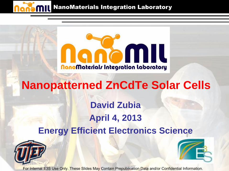
NanoMaterials Integration Laboratory
Nanopatterned ZnCdTe Solar Cells
David Zubia
April 4, 2013
Energy Efficient Electronics Science
For Internal E3S Use Only. These Slides May Contain Prepublication Data and/or Confidential Information.
NanoMaterials Integration Laboratory
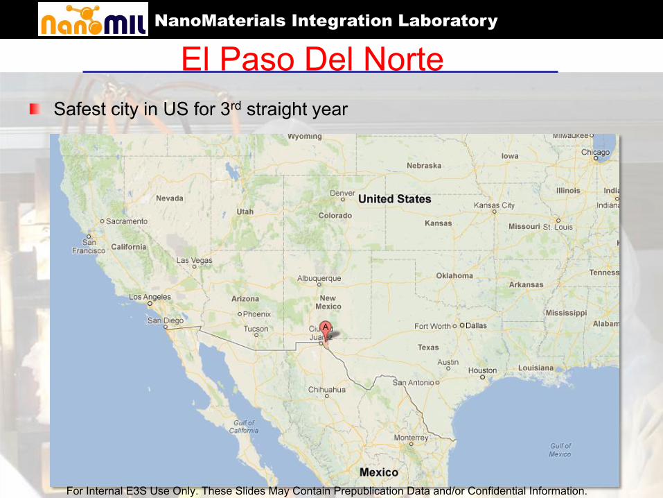
El Paso Del Norte Safest city in US for 3rd straight year
For Internal E3S Use Only. These Slides May Contain Prepublication Data and/or Confidential Information.
NanoMaterials Integration Laboratory
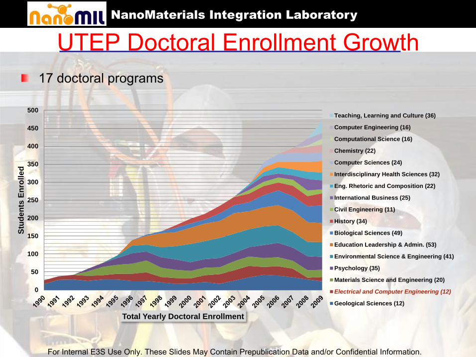
UTEP Doctoral Enrollment Growth 17 doctoral programs
0
50
100
150
200
250
300
350
400
450
500
Stu
den
ts E
nro
lle
d
Total Yearly Doctoral Enrollment
Teaching, Learning and Culture (36)
Computer Engineering (16)
Computational Science (16)
Chemistry (22)
Computer Sciences (24)
Interdisciplinary Health Sciences (32)
Eng. Rhetoric and Composition (22)
International Business (25)
Civil Engineering (11)
History (34)
Biological Sciences (49)
Education Leadership & Admin. (53)
Environmental Science & Engineering (41)
Psychology (35)
Materials Science and Engineering (20)
Electrical and Computer Engineering (12)
Geological Sciences (12)
For Internal E3S Use Only. These Slides May Contain Prepublication Data and/or Confidential Information.
NanoMaterials Integration Laboratory
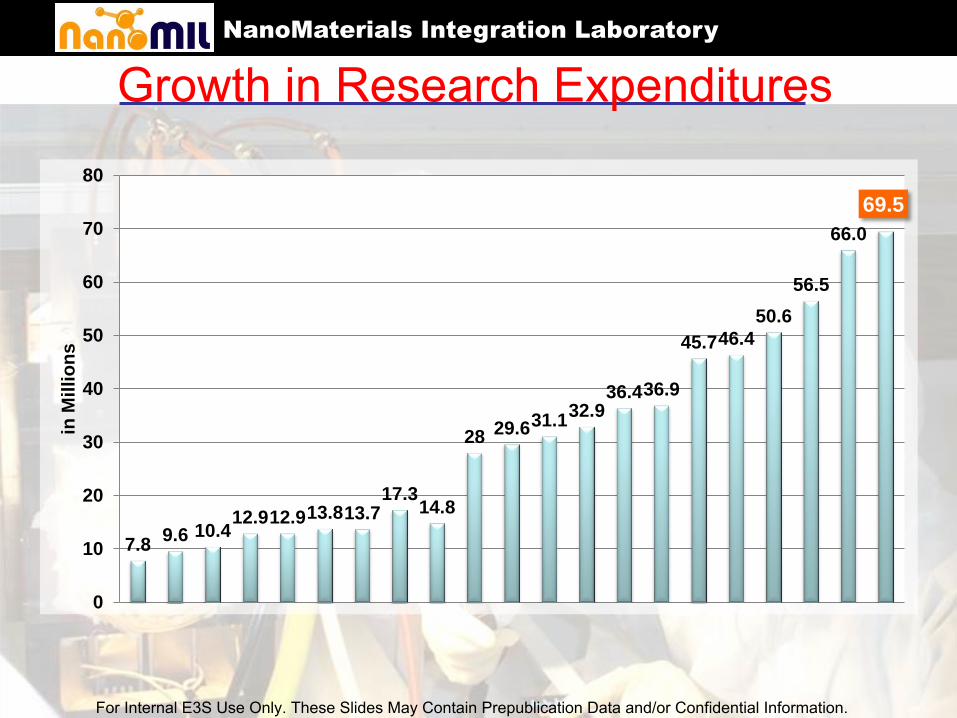
Growth in Research Expenditures
7.8 9.6 10.4
12.9 12.9 13.8 13.7 17.3
14.8
28 29.6 31.1 32.9
36.4 36.9
45.7 46.4
50.6
56.5
66.0
69.5
0
10
20
30
40
50
60
70
80
in M
illio
ns
For Internal E3S Use Only. These Slides May Contain Prepublication Data and/or Confidential Information.
NanoMaterials Integration Laboratory
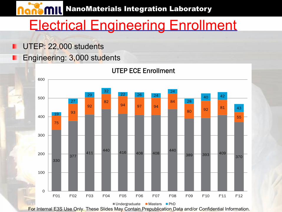
Electrical Engineering Enrollment UTEP: 22,000 students Engineering: 3,000 students
330
377 411
440 416 408 408
440
389 393 409 370
75
93
92
82 94 97 94
84
80 92
81
55 19
27
29 32
22 26 24 24
28 40 42
43
0
100
200
300
400
500
600
F'01 F'02 F'03 F'04 F'05 F'06 F'07 F'08 F'09 F'10 F'11 F'12
UTEP ECE Enrollment
Undergraduate Masters PhD
For Internal E3S Use Only. These Slides May Contain Prepublication Data and/or Confidential Information.
NanoMaterials Integration Laboratory
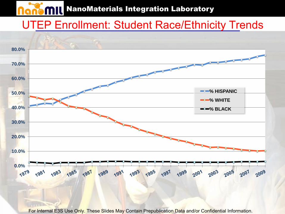
UTEP Enrollment: Student Race/Ethnicity Trends
0.0%
10.0%
20.0%
30.0%
40.0%
50.0%
60.0%
70.0%
80.0%
% HISPANIC
% WHITE
% BLACK
For Internal E3S Use Only. These Slides May Contain Prepublication Data and/or Confidential Information.
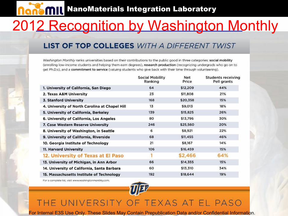
NanoMaterials Integration Laboratory
2012 Recognition by Washington Monthly
For Internal E3S Use Only. These Slides May Contain Prepublication Data and/or Confidential Information.
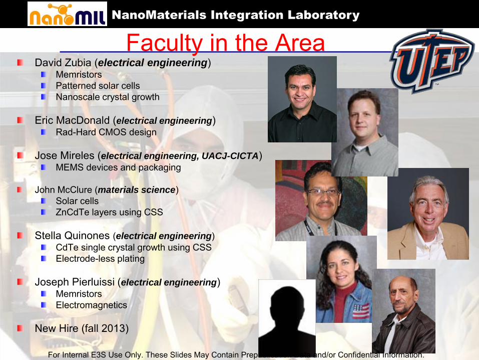
NanoMaterials Integration Laboratory
Faculty in the Area David Zubia (electrical engineering)
Memristors Patterned solar cells Nanoscale crystal growth
Eric MacDonald (electrical engineering) Rad-Hard CMOS design
Jose Mireles (electrical engineering, UACJ-CICTA)
MEMS devices and packaging
John McClure (materials science) Solar cells ZnCdTe layers using CSS
Stella Quinones (electrical engineering)
CdTe single crystal growth using CSS Electrode-less plating
Joseph Pierluissi (electrical engineering) Memristors Electromagnetics
New Hire (fall 2013)
For Internal E3S Use Only. These Slides May Contain Prepublication Data and/or Confidential Information.

NanoMaterials Integration Laboratory
Facilities
Science and Engineering Neighborhood
Campus Transformation
For Internal E3S Use Only. These Slides May Contain Prepublication Data and/or Confidential Information.

NanoMaterials Integration Laboratory
NanoFabrication Facility ~$5.0M investment
6,000 SF total, 2,500 SF clean
Class-100 & Class-1000
23 Major pieces of equipment
Teaching
Research
BS, MS, Ph. D. For Internal E3S Use Only. These Slides May Contain Prepublication Data and/or Confidential Information.

NanoMaterials Integration Laboratory
Research Lines Total Funding ~$5.3M
SnO2-based Memristors CdTe-based Solar Cells NSF, DOE, NINE
SiO2
~100 nmZnxCd(1-x)Te
Cadmium sulfide substrate
CdTe
Memristor Array Solar Cell Array
For Internal E3S Use Only. These Slides May Contain Prepublication Data and/or Confidential Information.
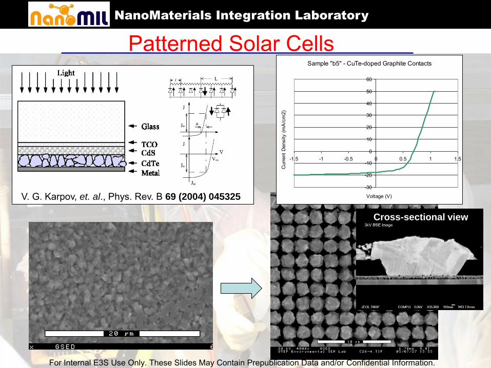
NanoMaterials Integration Laboratory
Patterned Solar Cells
V. G. Karpov, et. al., Phys. Rev. B 69 (2004) 045325
Sample "b5" - CuTe-doped Graphite Contacts
-30
-20
-10
0
10
20
30
40
50
60
-1.5 -1 -0.5 0 0.5 1 1.5
Voltage (V)
Cur
rent
Den
sity
(mA
/cm
2)
Cross-sectional view
For Internal E3S Use Only. These Slides May Contain Prepublication Data and/or Confidential Information.
NanoMaterials Integration Laboratory
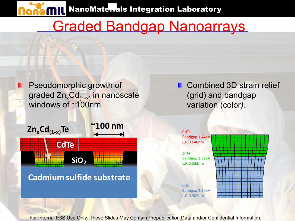
Graded Bandgap Nanoarrays
Pseudomorphic growth of graded ZnxCd(1-x) in nanoscale windows of ~100nm
SiO2
~100 nmZnxCd(1-x)Te
Cadmium sulfide substrate
CdTe
CdSBandgap 2.50eVL.P. 0.582nm
ZnTeBandgap 2.39eVL.P. 0.582nm
CdTeBandgap 1.44eVL.P. 0.648nm
c
Combined 3D strain relief (grid) and bandgap variation (color).
For Internal E3S Use Only. These Slides May Contain Prepublication Data and/or Confidential Information.
NanoMaterials Integration Laboratory
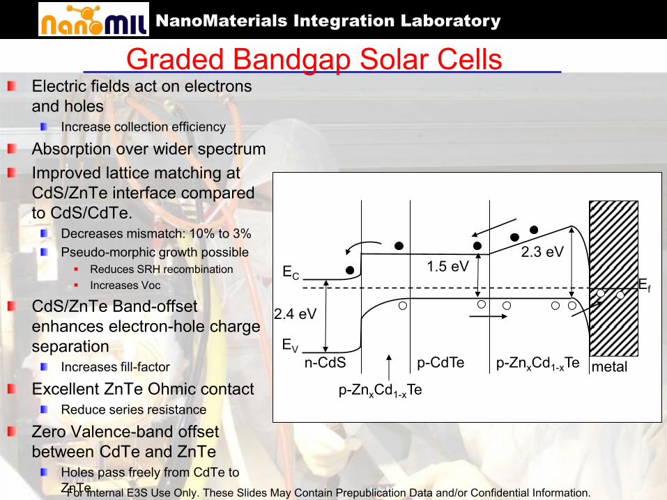
Graded Bandgap Solar Cells
Electric fields act on electrons and holes
Increase collection efficiency
Absorption over wider spectrum Improved lattice matching at CdS/ZnTe interface compared to CdS/CdTe.
Decreases mismatch: 10% to 3% Pseudo-morphic growth possible
Reduces SRH recombination Increases Voc
CdS/ZnTe Band-offset enhances electron-hole charge separation
Increases fill-factor
Excellent ZnTe Ohmic contact Reduce series resistance
Zero Valence-band offset between CdTe and ZnTe
Holes pass freely from CdTe to ZnTe
p-CdTe
p-ZnxCd1-xTe
p-ZnxCd1-xTe n-CdS
2.4 eV
1.5 eV 2.3 eV
Ef EC
EV metal
For Internal E3S Use Only. These Slides May Contain Prepublication Data and/or Confidential Information.

NanoMaterials Integration Laboratory
Experimental/Computational Collaboration
For Internal E3S Use Only. These Slides May Contain Prepublication Data and/or Confidential Information.
NanoMaterials Integration Laboratory
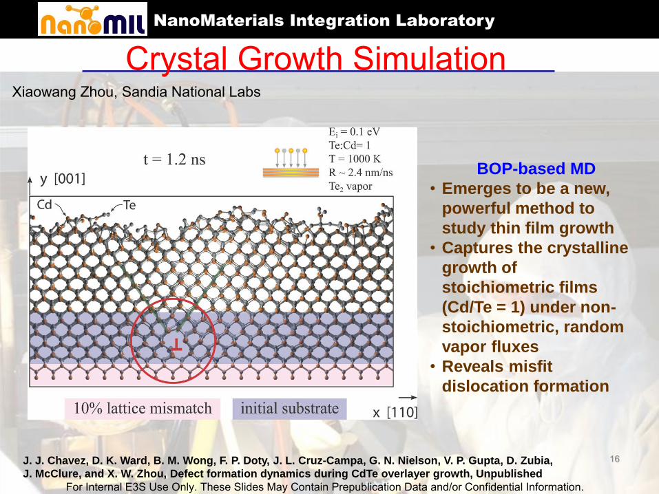
16
BOP-based MD
• Emerges to be a new,
powerful method to
study thin film growth
• Captures the crystalline
growth of
stoichiometric films
(Cd/Te = 1) under non-
stoichiometric, random
vapor fluxes
• Reveals misfit
dislocation formation
J. J. Chavez, D. K. Ward, B. M. Wong, F. P. Doty, J. L. Cruz-Campa, G. N. Nielson, V. P. Gupta, D. Zubia,
J. McClure, and X. W. Zhou, Defect formation dynamics during CdTe overlayer growth, Unpublished
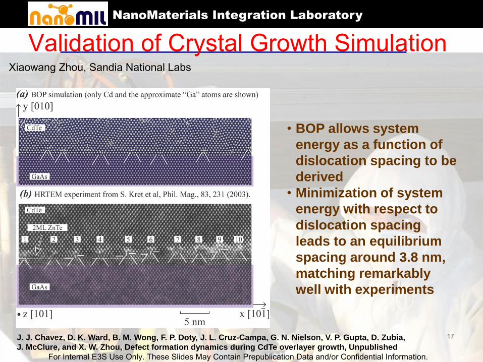
Crystal Growth Simulation Xiaowang Zhou, Sandia National Labs
For Internal E3S Use Only. These Slides May Contain Prepublication Data and/or Confidential Information.
NanoMaterials Integration Laboratory
17
• BOP allows system
energy as a function of
dislocation spacing to be
derived
• Minimization of system
energy with respect to
dislocation spacing
leads to an equilibrium
spacing around 3.8 nm,
matching remarkably
well with experiments
J. J. Chavez, D. K. Ward, B. M. Wong, F. P. Doty, J. L. Cruz-Campa, G. N. Nielson, V. P. Gupta, D. Zubia,
J. McClure, and X. W. Zhou, Defect formation dynamics during CdTe overlayer growth, Unpublished
Validation of Crystal Growth Simulation Xiaowang Zhou, Sandia National Labs
For Internal E3S Use Only. These Slides May Contain Prepublication Data and/or Confidential Information.
NanoMaterials Integration Laboratory
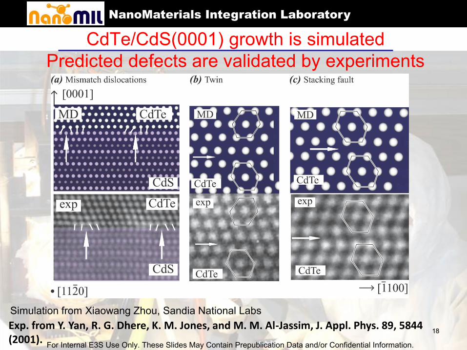
CdTe/CdS(0001) growth is simulated Predicted defects are validated by experiments
18 Exp. from Y. Yan, R. G. Dhere, K. M. Jones, and M. M. Al-Jassim, J. Appl. Phys. 89, 5844
(2001).
Simulation from Xiaowang Zhou, Sandia National Labs
For Internal E3S Use Only. These Slides May Contain Prepublication Data and/or Confidential Information.
NanoMaterials Integration Laboratory
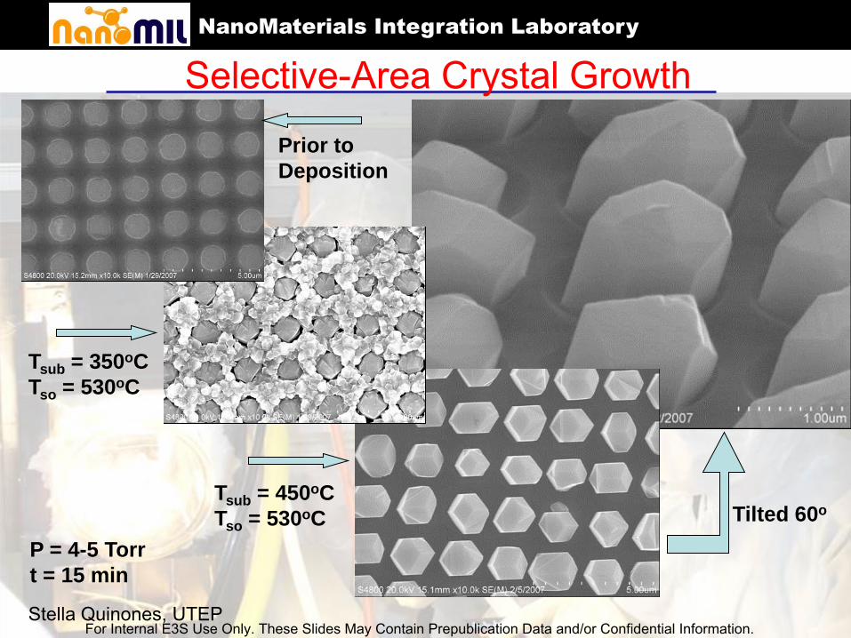
Selective-Area Crystal Growth
Tilted 60o
Prior to
Deposition
Tsub = 350oC
Tso = 530oC
Tsub = 450oC
Tso = 530oC
P = 4-5 Torr
t = 15 min
Stella Quinones, UTEP For Internal E3S Use Only. These Slides May Contain Prepublication Data and/or Confidential Information.
NanoMaterials Integration Laboratory
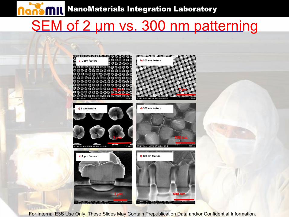
SEM of 2 µm vs. 300 nm patterning
2 𝝁m
b) 300 nm feature
20 𝝁m
a) 2 𝝁m feature
5 𝝁m 500 nm
400 nm 1 𝝁m
d) 300 nm feature c) 2 𝝁m feature
f) 300 nm feature e) 2 𝝁m feature
For Internal E3S Use Only. These Slides May Contain Prepublication Data and/or Confidential Information.

NanoMaterials Integration Laboratory
Diminishing the window size reduces the number of grains grown per window
21
Cross-section SEM View 1 𝝁m window size 130 nm window size
1 𝝁m 1 𝝁m Single crystal CdS
SiO2
SiO2
CdTe CdTe
Single crystal CdS
Multiple CdTe grains
Single CdTe seed?
21
Using a precision cutting tool ( Focused Ion beam or FIB)
and a SEM, we were able to see the difference in growth
using different window sizes of the nanopattern. Smaller
sizes are preferred For Internal E3S Use Only. These Slides May Contain Prepublication Data and/or Confidential Information.

NanoMaterials Integration Laboratory
EBSD indicates single domain in windows
Not patterned
22
50 µm
50 µm
2 µm
50 µm
50 µm
2 µm
(a) (b)
(c)
(e) (f)
(d)
2 µm pattern
300 nm pattern
For Internal E3S Use Only. These Slides May Contain Prepublication Data and/or Confidential Information.
NanoMaterials Integration Laboratory
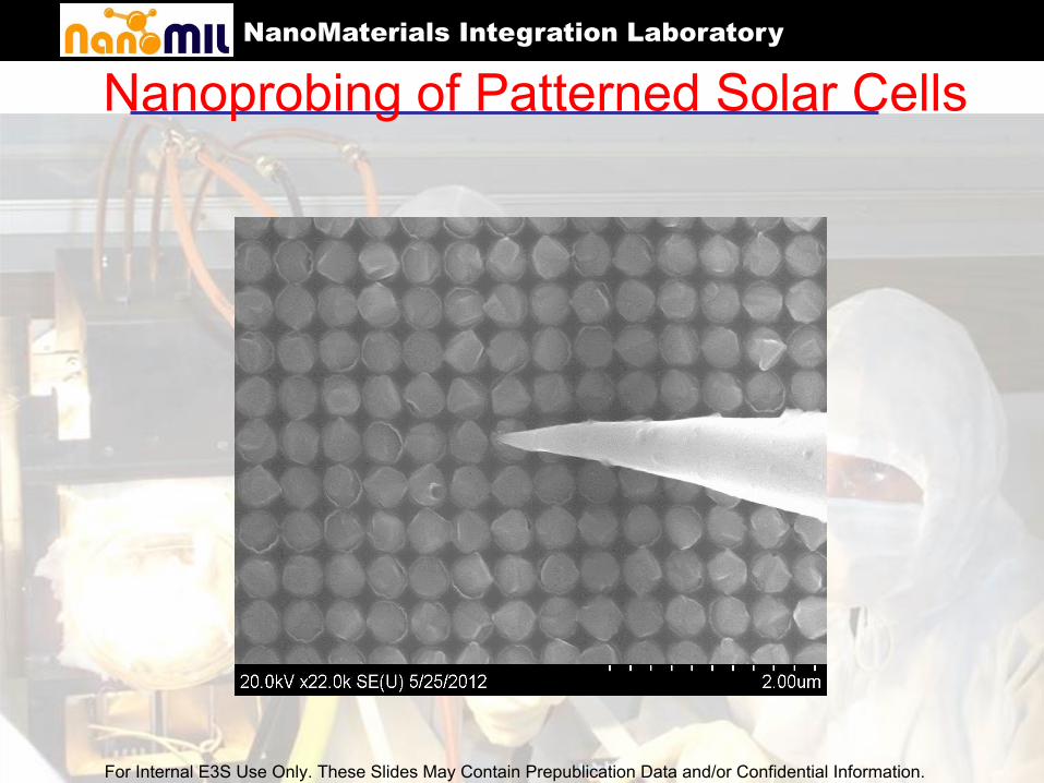
Nanoprobing of Patterned Solar Cells
For Internal E3S Use Only. These Slides May Contain Prepublication Data and/or Confidential Information.

NanoMaterials Integration Laboratory
Topology images and electric current maps can be obtained using conductive scanning AFM in contact mode
Area A
Area B
Area C
AFM Current Map
SiO2
CdTe
CdTe SiO2
AFM Voltage amplitude
image SEM Image AFM deflection
image
Shaved
Unshaved 24
For Internal E3S Use Only. These Slides May Contain Prepublication Data and/or Confidential Information.

NanoMaterials Integration Laboratory
IV data using conductive scanning AFM
IV on CdTe island IV on SiO2
- Zoom-in option in AFM system can be used to analyze individual CdTe islands. - Bright color denotes an area with high electric current (center image)
CdTe
SiO2
For Internal E3S Use Only. These Slides May Contain Prepublication Data and/or Confidential Information.
NanoMaterials Integration Laboratory
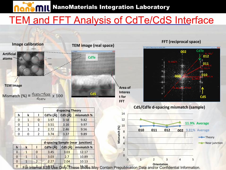
TEM and FFT Analysis of CdTe/CdS Interface
d-spacing Theory
h k l CdTe (Å) CdS (Å) mismatch %
0 1 0 3.97 3.58 9.82
0 1 1 3.51 3.16 9.97
0 1 2 2.72 2.46 9.56
0 0 2 3.74 3.37 9.89
d-spacing Sample (near junction)
h k l CdTe (Å) CdS (Å) mismatch %
0 1 0 3.45 3.03 12.17
0 1 1 3.03 2.7 10.89
0 1 2 2.27 2.04 10.13
0 0 2 3.13 2.78 11.18
0
2
4
6
8
10
12
14
0 1 2 3 4 5
Mis
mat
ch (
%)
Orientation
CdS/CdTe d-spacing mismatch (sample)
Theory
Near junction
010 011 012 002 9.81% Average
TEM image (real space) FFT (reciprocal space)
CdS
CdTe
CdS
CdTe
11.9% Average
TEM Image
Artificial atoms
Image calibration
Area of Interest for FFT
010
011
012 002
000
For Internal E3S Use Only. These Slides May Contain Prepublication Data and/or Confidential Information.
NanoMaterials Integration Laboratory
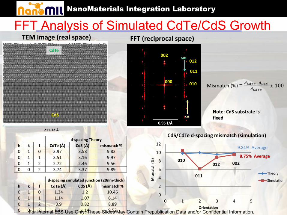
FFT Analysis of Simulated CdTe/CdS Growth
d-spacing Theory
h k l CdTe (Å) CdS (Å) mismatch %
0 1 0 3.97 3.58 9.82
0 1 1 3.51 3.16 9.97
0 1 2 2.72 2.46 9.56
0 0 2 3.74 3.37 9.89
d-spacing simulated junction (20nm-thick)
h k l CdTe (Å) CdS (Å) mismatch %
0 1 0 1.34 1.2 10.45
0 1 1 1.14 1.07 6.14
0 1 2 0.9 0.82 8.89
0 0 2 1.26 1.14 9.52
0
2
4
6
8
10
12
0 1 2 3 4 5
Mis
mat
ch (
%)
Orientation
CdS/CdTe d-spacing mismatch (simulation)
Theory
Simulation
010
011
012 002
9.81% Average
CdS
CdTe
211.32 Å
TEM image (real space) FFT (reciprocal space)
Note: CdS substrate is fixed
8.75% Average
010
011
012 002
000
For Internal E3S Use Only. These Slides May Contain Prepublication Data and/or Confidential Information.
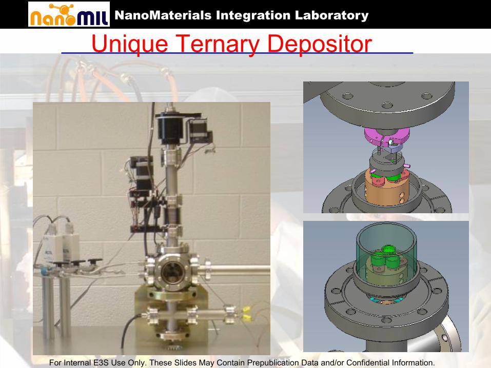
NanoMaterials Integration Laboratory
Unique Ternary Depositor
For Internal E3S Use Only. These Slides May Contain Prepublication Data and/or Confidential Information.
NanoMaterials Integration Laboratory
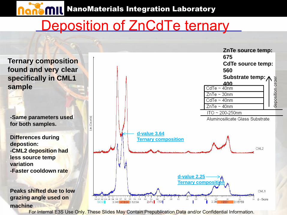
Deposition of ZnCdTe ternary
-Same parameters used
for both samples.
Differences during
depostion:
-CML2 deposition had
less source temp
variation
-Faster cooldown rate
Peaks shifted due to low
grazing angle used on
machine
d-value 3.64
Ternary composition
ZnTe source temp:
675
CdTe source temp:
560
Substrate temp:
400
Ternary composition
found and very clear
specifically in CML1
sample
d-value 2.25
Ternary composition
For Internal E3S Use Only. These Slides May Contain Prepublication Data and/or Confidential Information.
NanoMaterials Integration Laboratory
Acknowledgements Jose Cruz-Campa, Sandia National Labs Xiaowang Zhou, Sandia National Labs Doug Pete, Center for Integrated Nanotechnologies John McClure, UTEP Stella Quinones, UTEP Brandon Aguirre, UTEP Jose Chavez, UTEP Damian Marrufo, UTEP Abraham Alvarez, UTEP Francisco Alvarado, UTEP
For Internal E3S Use Only. These Slides May Contain Prepublication Data and/or Confidential Information.
NanoMaterials Integration Laboratory
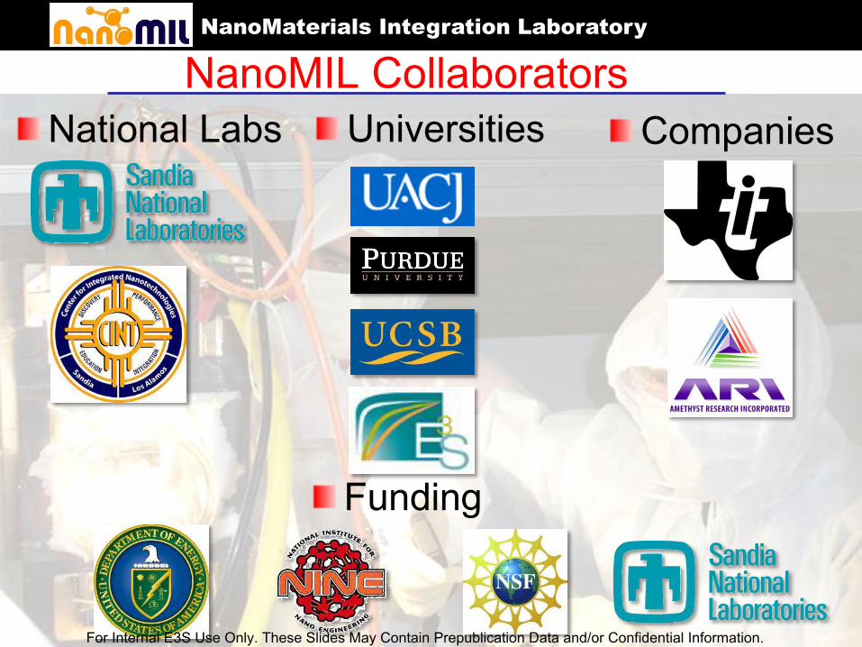
NanoMIL Collaborators Universities
National Labs
Funding
Companies
For Internal E3S Use Only. These Slides May Contain Prepublication Data and/or Confidential Information.
NanoMaterials Integration Laboratory
Thank you!
For Internal E3S Use Only. These Slides May Contain Prepublication Data and/or Confidential Information.