Embed Size (px)
Citation preview

Nanostructures Research GroupCENTER FOR SOLID STATE ELECTRONICS RESEARCH
Nanomanufacturing in Semiconductor Microelectronics
David K. FerryDepartment of Electrical Engineering and Center for Solid State Electronics Research
Arizona State University, Tempe, AZ
Second U.S.-Korea Forum on NanotechnologyFebruary 17-18, 2005, Los Angelos, CA

Nanostructures Research GroupCENTER FOR SOLID STATE ELECTRONICS RESEARCH
In 1954, a popular magazine asked “What would a home computer look like 50 years later, in 2004. Remember, there were very few computers of any kind at this time.

Nanostructures Research GroupCENTER FOR SOLID STATE ELECTRONICS RESEARCH
The new technology that revolutionized the computer, and the entire information processing world, was the creation by Texas Instruments and Intel of the microprocessor.
Intel 4004 microprocessor
Jack St. Clair KilbyNobel Prize 2000
Invention of the integrated circuit
T.I.s first integrated circuit

Nanostructures Research GroupCENTER FOR SOLID STATE ELECTRONICS RESEARCH
As integrated circuits became more dense and had smaller featuresizes, it was already clear that manufacturing was a problem:
Indeed, reduction in the theoretical minimum feature size has barely kept ahead of the research chips!
“…fabrication methods are limited by the general uncertainty relation, by scattering or by minimum size of photoresist molecules, …considerations of statistical doping fluctuations, …increases the minimum (feature) size to about 10 µm for a very complex (105 elements) circuit…”
J. T. Wallmark, Inst. Phys. Conf. Ser. 25, 133 (1975).

Nanostructures Research GroupCENTER FOR SOLID STATE ELECTRONICS RESEARCH
P. Gardini, Intel
Today’s production and pre-production

Nanostructures Research GroupCENTER FOR SOLID STATE ELECTRONICS RESEARCH
P. Gardini, Intel
Severe problems are already becoming apparent, and new concepts are needed

Nanostructures Research GroupCENTER FOR SOLID STATE ELECTRONICS RESEARCH
Manufacturing in the Si semiconductor industry is based upon one key technology, and that is the process of lithography and pattern transfer.
Lithography is essentially a photographic process, in which a pattern present in a mask is transferred to a photosensive material (the photo-resist) on the surface of the wafer.
Source
Lens
Lens
Mask
Wafer
This process is carried out by machines called “steppers” as they step across the wafer doing multiple exposures.
As much as 70% of the cost of a fab is lithography tools!
Nanostructures Research GroupCENTER FOR SOLID STATE ELECTRONICS RESEARCH
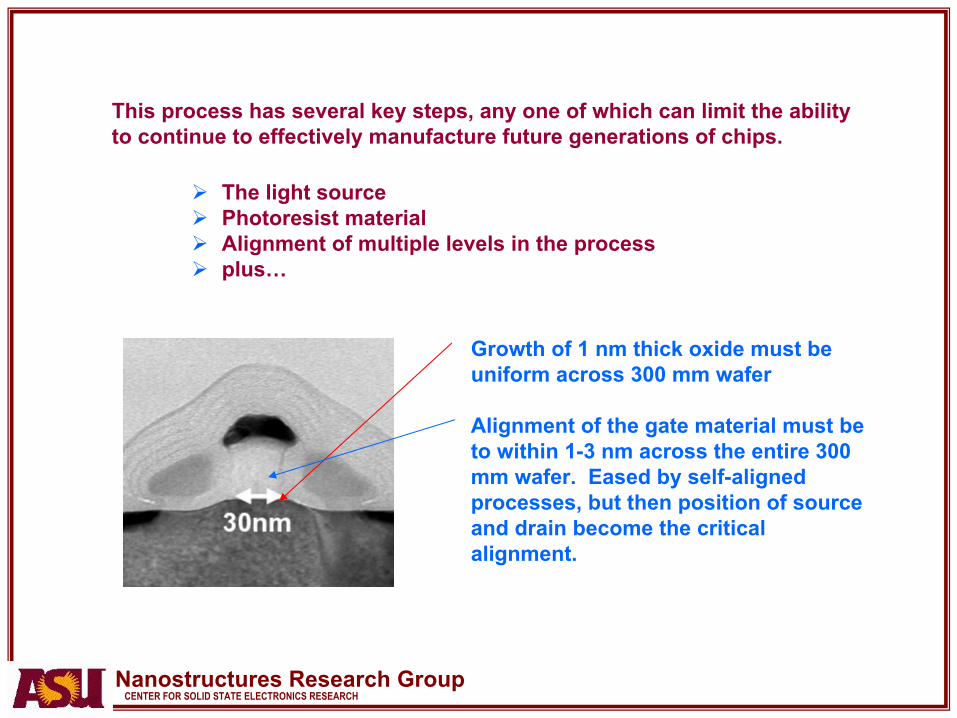
This process has several key steps, any one of which can limit the ability to continue to effectively manufacture future generations of chips.
The light sourcePhotoresist materialAlignment of multiple levels in the processplus…
Growth of 1 nm thick oxide must be uniform across 300 mm wafer
Alignment of the gate material must be to within 1-3 nm across the entire 300 mm wafer. Eased by self-aligned processes, but then position of source and drain become the critical alignment.

Nanostructures Research GroupCENTER FOR SOLID STATE ELECTRONICS RESEARCH
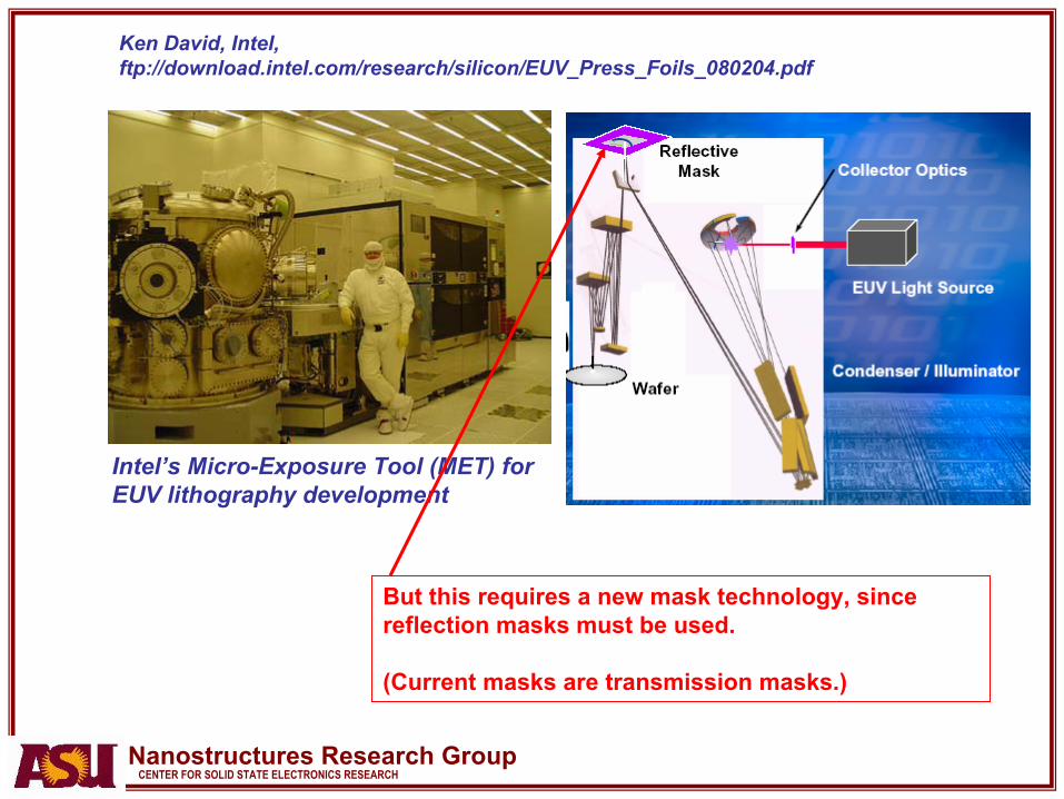
As we move beyond critical dimensions of 30 nm in today’s devices, new exposure tools will be required—use of 193 nm wave length light in air will no longer produce the resolution required.
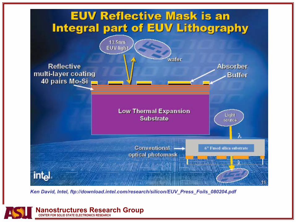
One new approach is with Extreme Ultra-Violet (EUV) with 13.5 nm wavelength.
Ken David, Intel, ftp://download.intel.com/research/silicon/EUV_Press_Foils_080204.pdf
Nanostructures Research GroupCENTER FOR SOLID STATE ELECTRONICS RESEARCH
Intel’s Micro-Exposure Tool (MET) for EUV lithography development
But this requires a new mask technology, since reflection masks must be used.
(Current masks are transmission masks.)
Ken David, Intel, ftp://download.intel.com/research/silicon/EUV_Press_Foils_080204.pdf
Nanostructures Research GroupCENTER FOR SOLID STATE ELECTRONICS RESEARCH
Ken David, Intel, ftp://download.intel.com/research/silicon/EUV_Press_Foils_080204.pdf

Nanostructures Research GroupCENTER FOR SOLID STATE ELECTRONICS RESEARCH
We also need to develop new or improved resists, as resist development is definitely hindered by exposure tool resolution and by process variability. We need both: better resolution and controlled processing.
Small lines (≥6 nm) obtained in PMMA
M. Khoury and D. K. Ferry, JVST B 14, 75 (1996).
But, PMMA (the highest resolution resist) is generally thought to be too slow for industrial use.

Nanostructures Research GroupCENTER FOR SOLID STATE ELECTRONICS RESEARCH
At ASU, we are also pursuing studies of ZEP-520, a faster high resolution resist, in our JEOL 6000 e-beam system for ultra-high resolution (approaching that of PMMA).This resist should also be usable by EUV tools.

Nanostructures Research GroupCENTER FOR SOLID STATE ELECTRONICS RESEARCH
The process of nanofabrication is expected to get much more detailed in coming years. This is not just because of reduced dimensions and constraints on lithography.
Device structures will get more complicated.
Intel Tri-gate structureR. Chau, Intel
Semiconductornanowires
Gated vertical CNT concept (Siemens)

Nanostructures Research GroupCENTER FOR SOLID STATE ELECTRONICS RESEARCH
Low-K dielectric
Metal(copper)
The idea of using vertical devices, either at the Sisurface, or in the interconnect layers, opens the door to novel new reconfigurable logic circuits.
Cross-section of Intel Pentium metallization layers.

Nanostructures Research GroupCENTER FOR SOLID STATE ELECTRONICS RESEARCH
ZnO Nanowire MOS Transistors
Ng et al., Nanolett. 4, 1247 (2004).
Nanostructures Research GroupCENTER FOR SOLID STATE ELECTRONICS RESEARCH
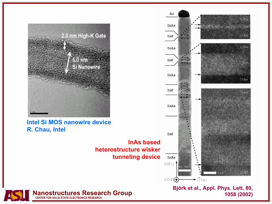
Intel Si MOS nanowire deviceR. Chau, Intel
InAs based heterostructure wisker
tunneling device
Björk et al., Appl. Phys. Lett. 80, 1058 (2002)

Nanostructures Research GroupCENTER FOR SOLID STATE ELECTRONICS RESEARCH
One important question is: Will device operation change at these small sizes? That is, will the physics of the device limit how small we can make transistors?
This question has been addressed for as many decades as we have been making integrated circuits.
As pointed out earlier, the theoretical limiting size has been going down continuously with the device scaling.
Can we address this question in a better manner?

Nanostructures Research GroupCENTER FOR SOLID STATE ELECTRONICS RESEARCH
Semi-classical modeling of semiconductor devices has proceeded to where we have very efficient ensemble Monte Carlo techniques which caninvestigate detailed many-body effects in small devices, as well as surface-roughness, discrete doping, random potentials, etc.
On the other hand, device down-scaling is approaching a size which is comparable to the carrier coherence length, and within an order of magnitude or so of the de Broglie thermal wavelength.
Many approximate techniques for first-order quantum corrections have been proposed: density gradient, effective potential, etc. These are not adequate on this size scale.
This means that new, fully quantum mechanical approaches are needed to study the coherent quantum behavior in these devices.
Ours is not the first such simulation, and others have used direct solutions of the Schrödinger equation, Green’s functions, quantum hydrodynamic equations, etc. We feel that our approach is better, and allows us to incorporate scattering effectively, while being more computationally efficient than e.g. Green’s functions.

Nanostructures Research GroupCENTER FOR SOLID STATE ELECTRONICS RESEARCH
For our systems, we can generate a relatively straight-forward loop to find the solutions:
Solve for ψ(x,y,z) with recursive scattering
matrix from bothright and left
Find ρ
Solve forV(x,y,z)
Correct forExchange,
Correlation, etc.
Often requires the Fermi energy to be adjusted to keep density constant.

Nanostructures Research GroupCENTER FOR SOLID STATE ELECTRONICS RESEARCH
36.93 nmSource
20.64 nm
Drain
20.64 nmChannel
Oxide
Oxide
19.55 nm
19.55 nm
Y
X 60.83 nm
We initially consider a relative large cross-section device, whose properties are nearly bulk-like. Impurities are considered exactly within the Poisson equation.

Nanostructures Research GroupCENTER FOR SOLID STATE ELECTRONICS RESEARCH
0
200
400
600
800
1000
1200
1400
1016 1017 1018 1019 1020 1021
µ n(cm
2 /Vs)
Doping Concentration (cm-3)
Closed symbols are the calculated mobility, limited by impurity and phonon scattering.
Open symbols are experimental
results taken from the literature.

Nanostructures Research GroupCENTER FOR SOLID STATE ELECTRONICS RESEARCH
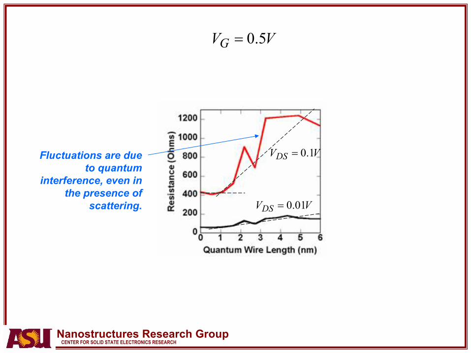
Then we go to a smaller device, and vary the channel length. For devices, in which phonon and impurity scattering dominate ballistic transport, the resistance will increase with the length of the channel.
GL
Nanostructures Research GroupCENTER FOR SOLID STATE ELECTRONICS RESEARCH
VVG 5.0=
VVDS 1.0=
VVDS 01.0=
Fluctuations are due to quantum
interference, even in the presence of
scattering.
Nanostructures Research GroupCENTER FOR SOLID STATE ELECTRONICS RESEARCH
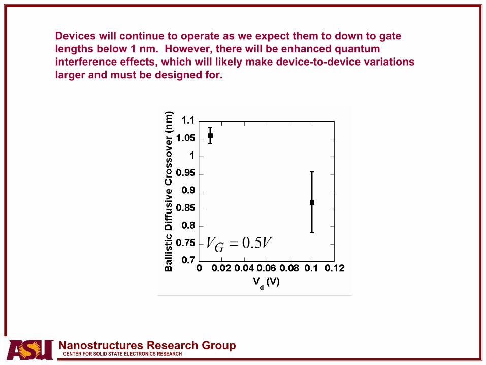
VVG 5.0=
Devices will continue to operate as we expect them to down to gate lengths below 1 nm. However, there will be enhanced quantum interference effects, which will likely make device-to-device variations larger and must be designed for.

Nanostructures Research GroupCENTER FOR SOLID STATE ELECTRONICS RESEARCH
Manufacturing is a major part of the scaling of integrated circuits to ever smaller dimensions.
One key ingredient in integrated circuits is lithography, and new tools are continuing to be developed each year. The requirements, in terms of resolution and alignment, continue to become more exacting with parts per billion expected today and exponentially more exacting factors expected in the future.
Nevertheless, we see no physical limitations on the performance of today’s FETs for several generations into the future.