Embed Size (px)
Citation preview

Nanoelectronics in Indian Academia: Present and Future:
a policy & implementation perspective
Udayan GangulyJune 10, 2014
Collated based on discussions with Saurabh Lodha, Swaroop Ganguly, Bipin Rajendran, Souvik Mahapatra, Anil Kottantharayil, V Ramgopal Rao, Juzer Vasi
U Ganguly Assocham 2014 2
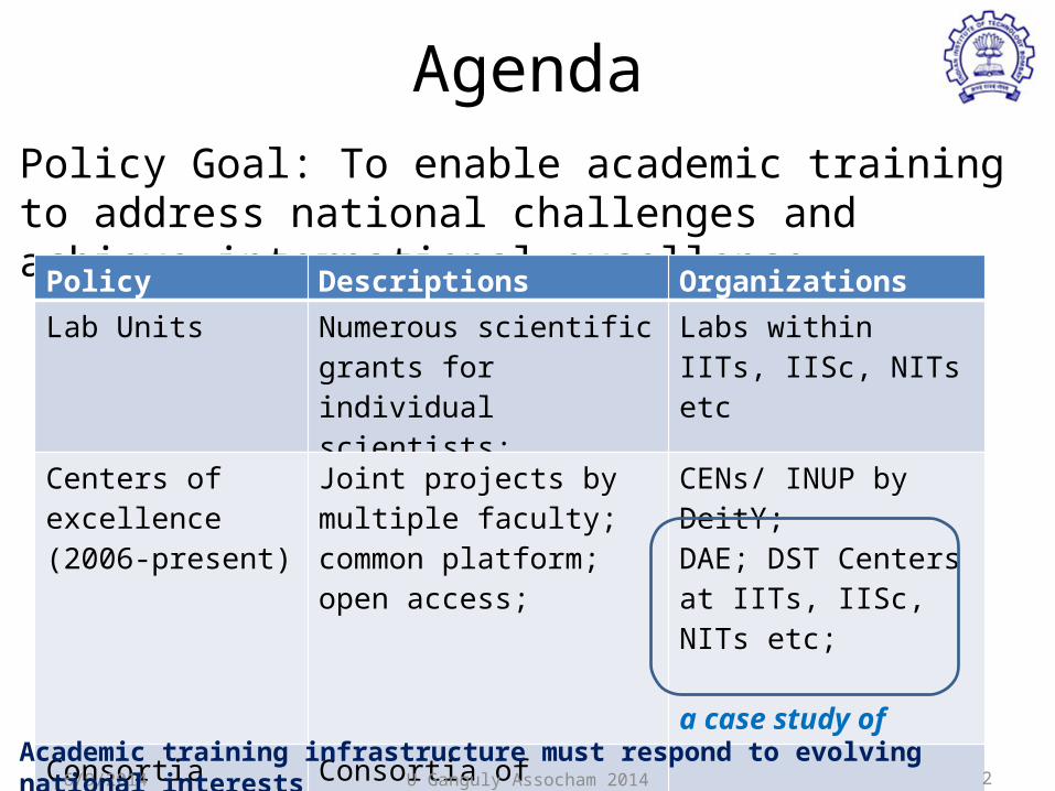
AgendaPolicy Goal: To enable academic training to address national challenges and achieve international excellence
Policy Descriptions Organizations
Lab Units Numerous scientific grants for individual scientists;
Labs within IITs, IISc, NITs etc
Centers of excellence (2006-present)
Joint projects by multiple faculty; common platform; open access;
CENs/ INUP by DeitY;DAE; DST Centers at IITs, IISc, NITs etc;
a case study of IITBNF
Consortia (2014 …) Consortia of academia/industry for prototyping, incubation & training;
A proposal for future
6/9/2014Academic training infrastructure must respond to evolving national interests

U Ganguly Assocham 2014 3
• Mission and Vision
• Nanoelectronics Research Evolution @ IITBNF
• Key Achievements
• IITBNF Organization and Operational Highlights
• Future of Nanotechnology @ IITB – A Proposal
Outline
6/9/2014

IIT Bombay Nanofabrication Facility
250 Crores ($ 50M) facility More than 300 researcher students & 66 faculty members
“I have been extremely impressed … one of the leading universities in the world in the field of technology” - Mr. Joe Biden, July 2013
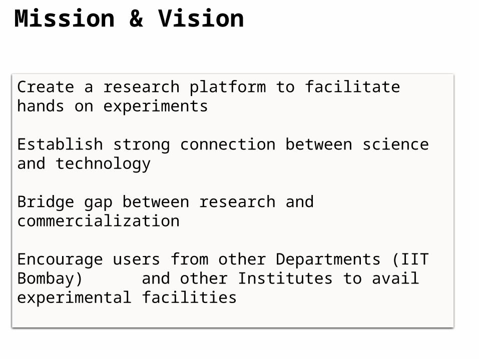
Mission & Vision
Create a research platform to facilitate hands on experiments
Establish strong connection between science and technology
Bridge gap between research and commercialization
Encourage users from other Departments (IIT Bombay) and other Institutes to avail experimental facilities
U Ganguly Assocham 2014 6
IITBNF
National Tech
Education (NPE)
GoI PolicyIncubation
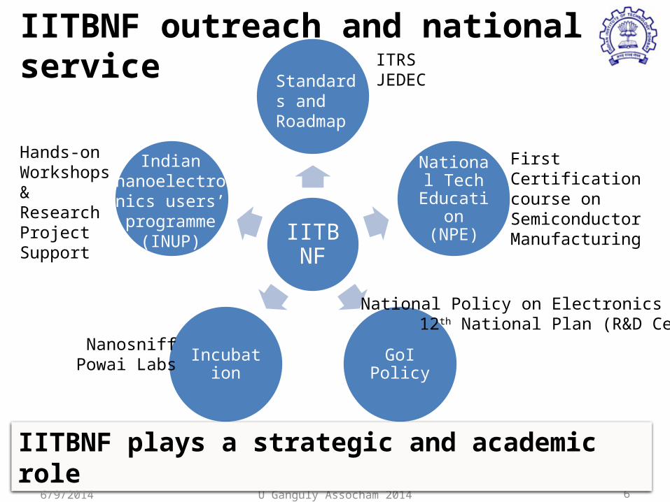
IITBNF outreach and national service
National Policy on Electronics (NPE)12th National Plan (R&D Center)
NanosniffPowai Labs
ITRS JEDEC
First Certification course on Semiconductor Manufacturing
Hands-on Workshops& Research Project Support
IITBNF plays a strategic and academic role
Standards and Roadmap
Indian nanoelectronics
users’ programme
(INUP)
6/9/2014

U Ganguly Assocham 2014 7
Timeline & Funding of IITBNF
2006 2007 2008 2009 2010 2011 2012 2013
Centre for Excellence in Nanoelectronics (CEN), DeitY, 50 Cr
Equipment donation - Nanomanufacturing Lab, CLEAN Lab (~ 32 Cr AMAT)Sponsored projects (7.5 Cr AMAT)
INUP DeitY, 12 Cr
Sponsored projects - R&D Organizations (~ 58 Cr)
NCPRE MNRE, 45 Cr
Infrastructure - IITB, 15 Cr
Industry partners (Intel, TSMC, IBM, TI, Micron, Synopsys, Maxim, Renesas, 7.5 Cr)
CEN, DeitY, 80Cr
INUP 35 Cr
6/9/2014
U Ganguly Assocham 2014 88
2006 2007 2008 2009 2010 2011 2012 2013
CEN, DIT, $10M
IITB, $ 3M
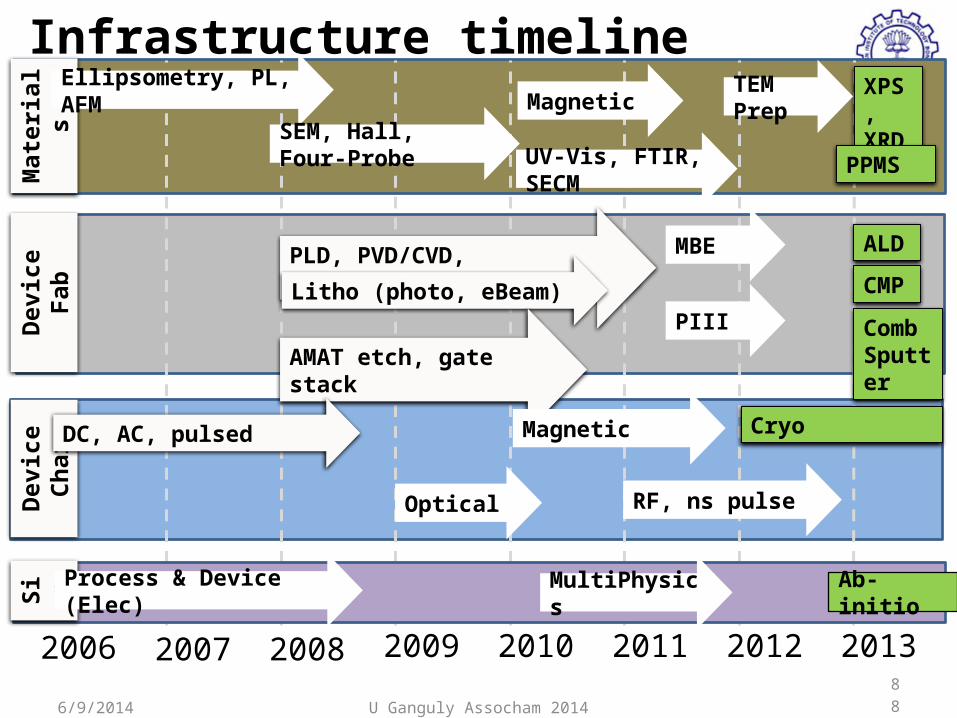
Infrastructure timelineM
ater
ials
Dev
ice
Fab
Dev
ice
Char
XPS, XRD
ALD
CMP
Comb Sputter
Cryo
Sim
Ellipsometry, PL, AFM
SEM, Hall, Four-Probe
Magnetic
PLD, PVD/CVD, Evaporation, Sputter
Litho (photo, eBeam)
AMAT etch, gate stack
MBE
PIII
DC, AC, pulsed Magnetic
Optical RF, ns pulse
Ab-initioMultiPhysicsProcess & Device (Elec)
PPMSUV-Vis, FTIR, SECM
TEM Prep
6/9/2014
U Ganguly Assocham 2014 99
2006 2007 2008 2009 2010 2011 2012 2013
CEN, DIT, $10M
IITB, $ 3M
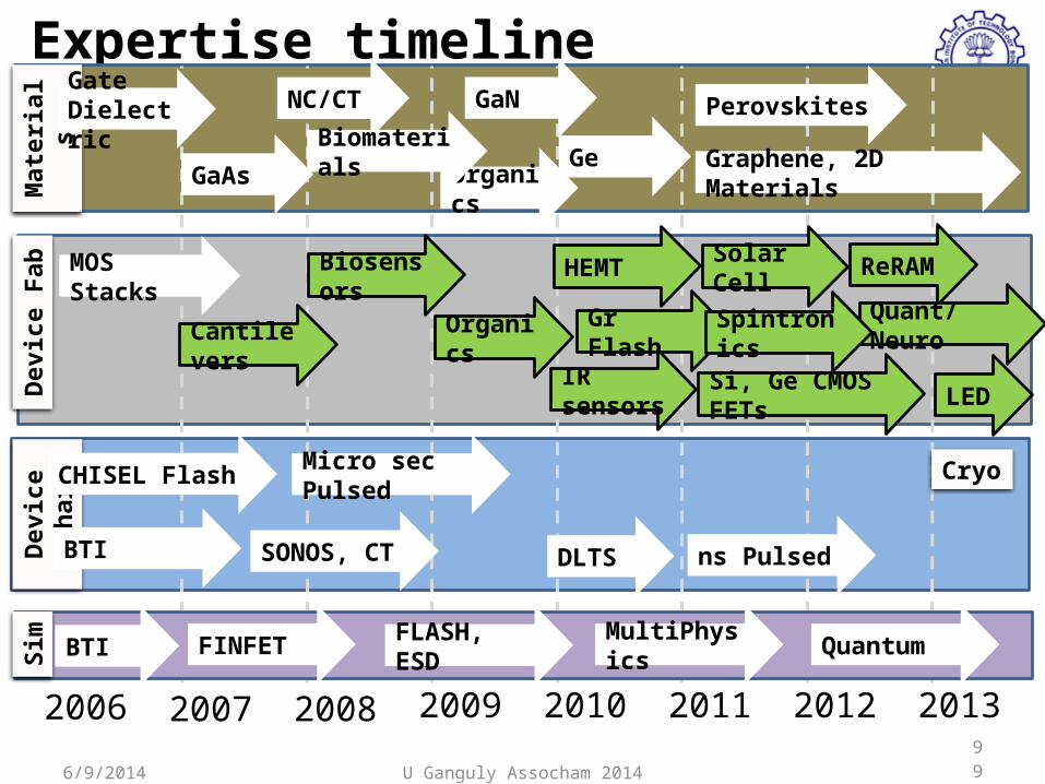
Expertise timelineM
ater
ials
Dev
ice
Fab
Dev
ice
Char
Sim
Graphene, 2D Materials
Perovskites
Ge
GaN
GaAs
Gate Dielectric
NC/CT
MOS Stacks HEMT ReRAM
Si, Ge CMOS FETs
Gr Flash
CHISEL Flash
DLTS
Micro sec Pulsed
ns PulsedSONOS, CTBTI
BTI FLASH, ESD MultiPhysics Quantum
Cryo
Quant/Neuro
IR sensors LED
Cantilevers
Biosensors
Organics
Solar Cell
OrganicsBiomaterials
Spintronics
FINFET
6/9/2014
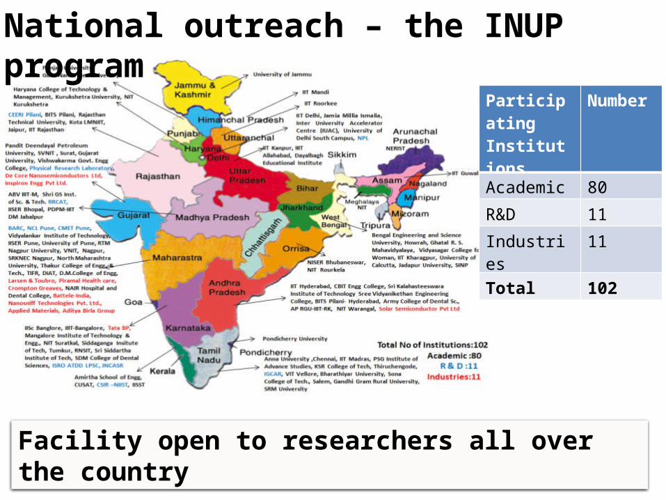
National outreach – the INUP program
Facility open to researchers all over the country
Participating Institutions
Number
Academic 80
R&D 11
Industries 11
Total 102

U Ganguly Assocham 2014 11
Research Output and Achievements
• Papers in High Impact Journals (2006-2013): >200– IEEE Transactions on ED,
Nanotechnology, IM– IEEE EDL– AIP APL, JAP– ACS Nano– J-MEMS– Organic Electronics– IOP Nanotechnology
• Presence in top international conferences– Logic and Memory Devices– Photovoltaics– Spintronics – MEMS– Material Growth
IRPSIED
M DRCIM
W
ESSD
ERC
VLSI Te
ch SISC
SISPAD
PVSC
MMM/Inter
magMEM
SMRS
NAMBEISC
S
Euro
MBE
0
2
4
6
8
10
12
14
16
18
20Key Conference Publications (2006-2013)
Logic and Memory Devices
Materials Growth
PV
Simulation
Spin
MEMS
IITBNF enables high impact research in diverse areas
6/9/2014
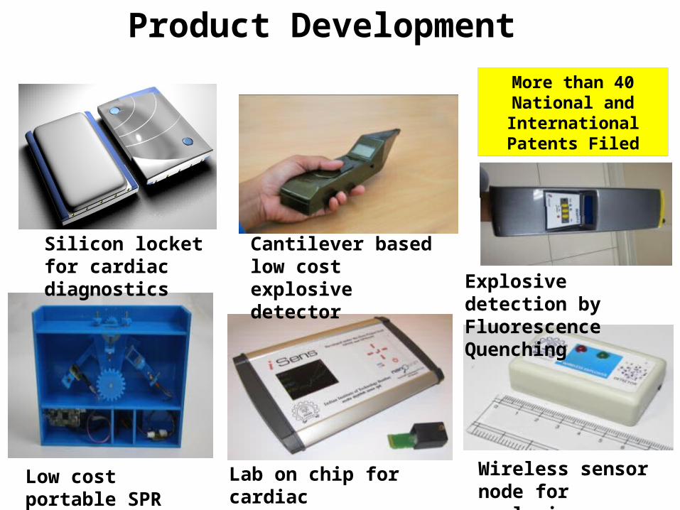
Product Development
Wireless sensor node for explosive detection
Lab on chip for cardiac diagnostics
Low cost portable SPR
Silicon locket for cardiac diagnostics
Cantilever based low cost explosive detector
Explosive detection by Fluorescence Quenching
More than 40 National and International
Patents Filed

U Ganguly Assocham 2014 13
IITBNF Organizational Structure
FOC [Facility Oversight committee, 24F + 41S]Faculty [F] : Making Rules/Policies
Staff [S]: Implementing Policies
Equipment Operations Committe
e[3F + 14S]
Equipment Maintenanc
e Committee [3F + 3S]
Public Relations Committee [2F + 3S]
Inventory
Committe
e[2F + 3S]
HR Committe
e[2F + 2S]
Admin
Committe
e[3F + 15S]
IT Committe
e[3F + 4S]
Disciplinary Committe
e[5F + 2S]
Safety Committe
e[3F+ 8S]
Facility
Committe
e[3F+ 8S]
Professionally run national facility with 24x7 operation19
21
2
EEPhysicsEnergy SciencesBiosciences
Dept NumberEE 19
Physics 2Energy Sciences 1
Biosciences 2Total 24
6/9/2014
U Ganguly Assocham 2014 14
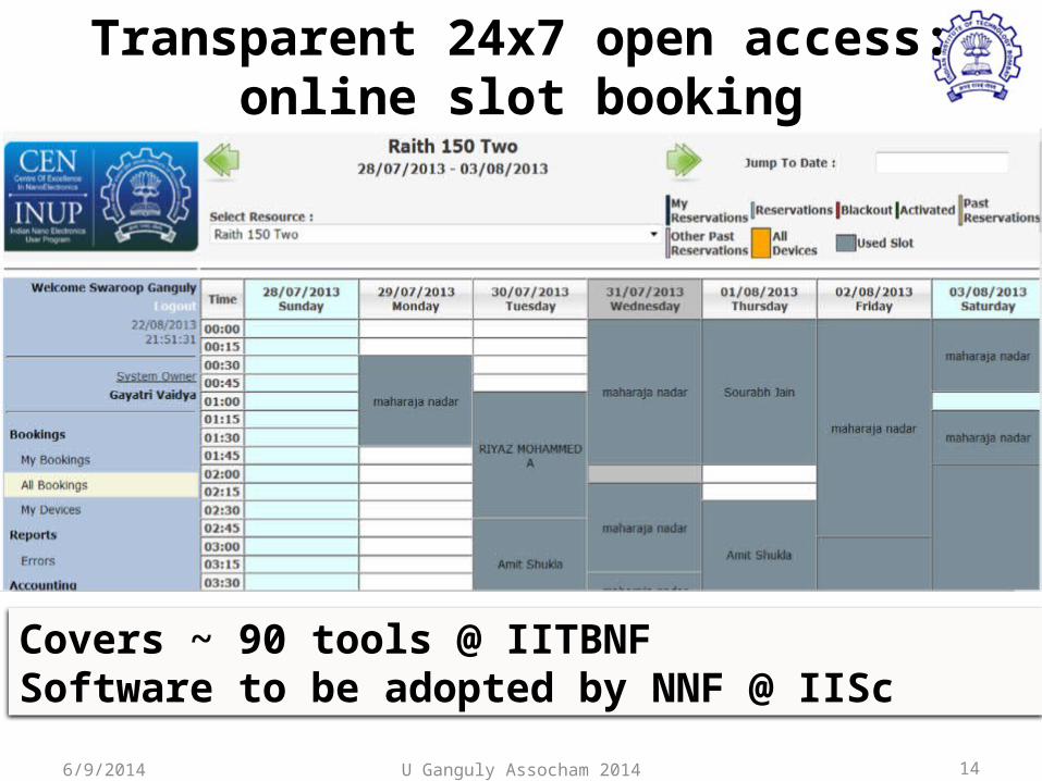
Transparent 24x7 open access: online slot booking
Covers ~ 90 tools @ IITBNFSoftware to be adopted by NNF @ IISc
6/9/2014
U Ganguly Assocham 2014 15
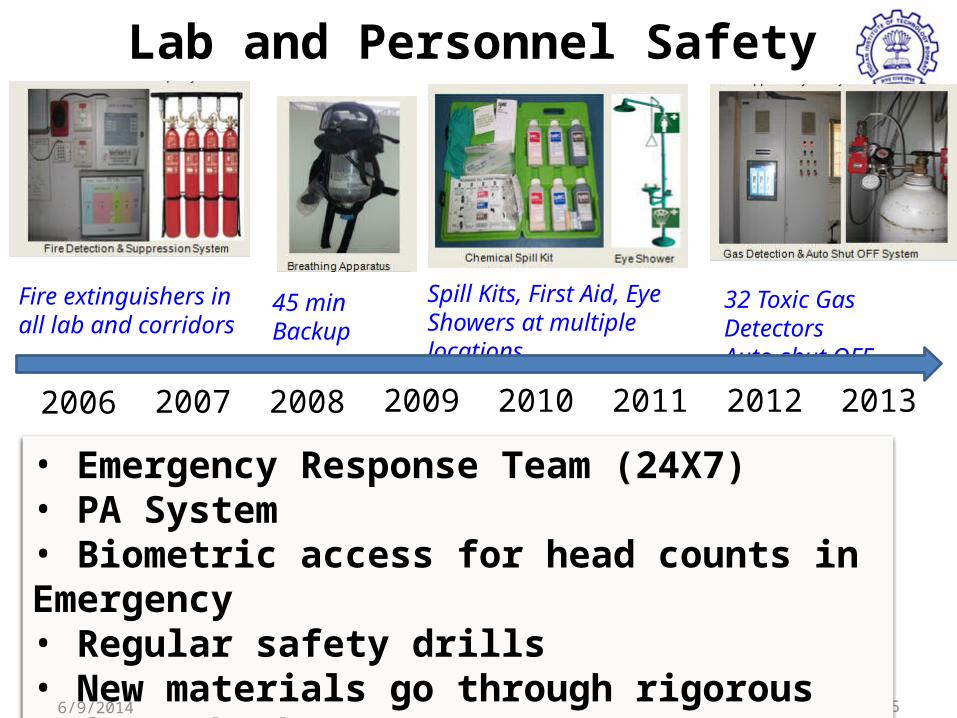
Lab and Personnel Safety
32 Toxic Gas DetectorsAuto-shut OFF
Fire extinguishers in all lab and corridors
45 min Backup Spill Kits, First Aid, Eye Showers at multiple locations
• Emergency Response Team (24X7)• PA System• Biometric access for head counts in Emergency• Regular safety drills • New materials go through rigorous safety checks
2006 2007 2008 2009 2010 2011 2012 2013
6/9/2014
U Ganguly Assocham 2014 16
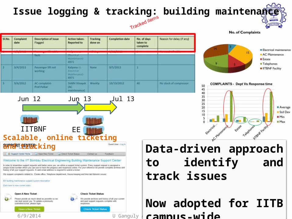
Issue logging & tracking: building maintenance
Data-driven approach to identify and track issues Now adopted for IITB campus-wide maintenance
Scalable, online ticketing and tracking
Jun 12 Jun 13 Jul 13
IITBNF EE
6/9/2014
U Ganguly Assocham 2014 17
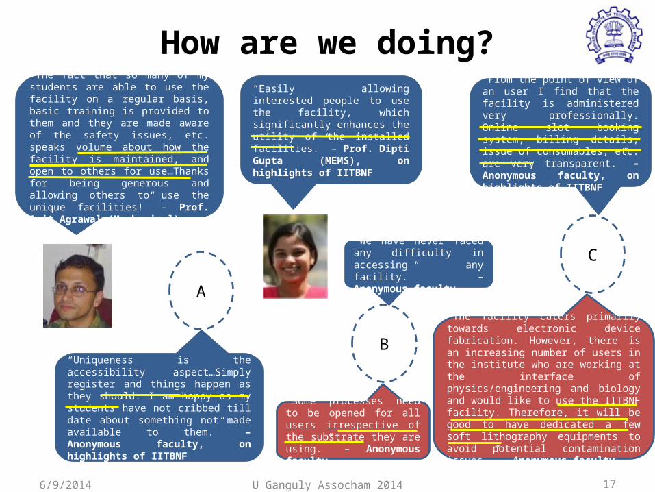
“The fact that so many of my students are able to use the facility on a regular basis, basic training is provided to them and they are made aware of the safety issues, etc. speaks volume about how the facility is maintained, and open to others for use…Thanks for being generous and allowing others to use the unique facilities!” – Prof. Amit Agrawal (Mechanical)
“Easily allowing interested people to use the facility, which significantly enhances the utility of the installed facilities.” – Prof. Dipti Gupta (MEMS), on highlights of IITBNF
How are we doing?
“Uniqueness is the accessibility aspect…Simply register and things happen as they should. I am happy as my students have not cribbed till date about something not made available to them.” – Anonymous faculty, on highlights of IITBNF
“The facility caters primarily towards electronic device fabrication. However, there is an increasing number of users in the institute who are working at the interface of physics/engineering and biology and would like to use the IITBNF facility. Therefore, it will be good to have dedicated a few soft lithography equipments to avoid potential contamination issues.” – Anonymous faculty
C“We have never faced any difficulty in accessing any facility.” – Anonymous faculty
“Some processes need to be opened for all users irrespective of the substrate they are using.” – Anonymous faculty
B
A
“From the point of view of an user I find that the facility is administered very professionally. Online slot booking system, billing details, issue of consumables, etc. are very transparent.” – Anonymous faculty, on highlights of IITBNF
6/9/2014

U Ganguly Assocham 2014 18
Faculty and Student Participation
biosciences8%
energy11%
chemical6%
chemistry3%
electrical30%
mechanical6%
metallurgical15%
physics21%
Facultybiosciences
6% chemical1%
chemistry2%
crnts8%
electrical32%
energy11%environmental
1%
mechanical5%
metallurgical15%
physics19%
PhD Students
biosciences 10chemical 2chemistry 3crnts 13electrical 51energy 17environmental 1mechanical 8metallurgical 24physics 30
159
Strong inter-disciplinary focus and open access
6/9/2014
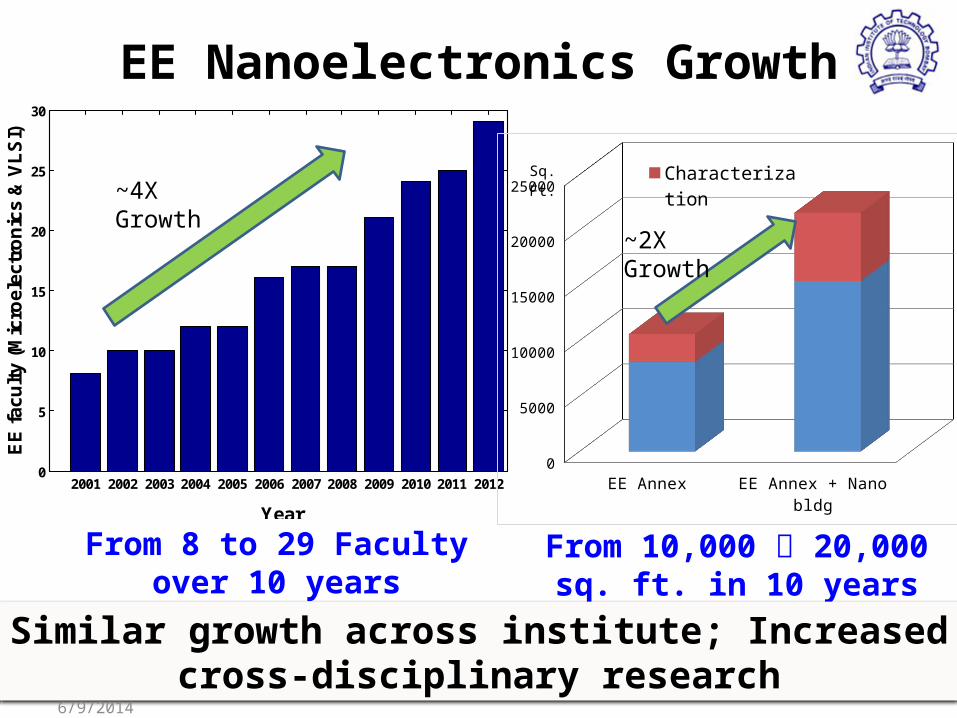
EE Nanoelectronics Growth
U Ganguly Assocham 2014 19
2001 2002 2003 2004 2005 2006 2007 2008 2009 2010 2011 20120
5
10
15
20
25
30
Year
EE
fac
ult
y (M
icro
elec
tro
nic
s &
VL
SI)
~4X Growth
From 8 to 29 Faculty over 10 years
EE Annex EE Annex + Nano bldg0
5000
10000
15000
20000
25000CharacterizationFabrication
Sq. Ft.
~2X Growth
From 10,000 20,000 sq. ft. in 10 years
Similar growth across institute; Increased cross-disciplinary research
6/9/2014
U Ganguly Assocham 2014 20
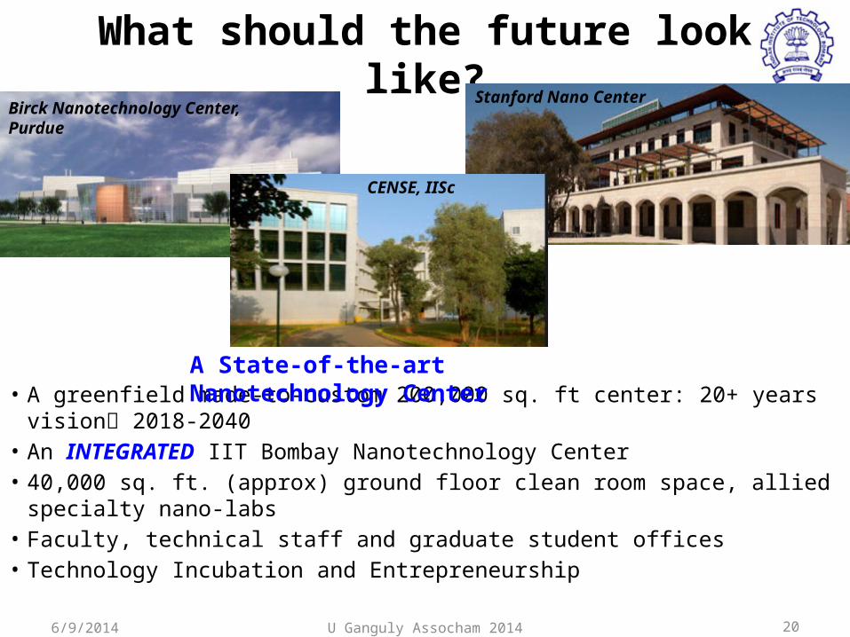
What should the future look like?
• A greenfield made-to-custom 200,000 sq. ft center: 20+ years vision 2018-2040• An INTEGRATED IIT Bombay Nanotechnology Center• 40,000 sq. ft. (approx) ground floor clean room space, allied specialty nano-labs • Faculty, technical staff and graduate student offices• Technology Incubation and Entrepreneurship
Birck Nanotechnology Center, PurdueStanford Nano Center
CENSE, IISc
A State-of-the-art Nanotechnology Center
6/9/2014

U Ganguly Assocham 2014 21
India’s Need for Semiconductor Manufacturing
Electronics production value chain
Strong need for semiconductor manufacturing to increase electronic production
Source: Applied Materials
Design + Manufacturing = Products
• Semiconductors are the basic building block for all electronics products– 25-30% of product value (even higher for PDA, Tablets, Mobile Phone etc.)
• Semiconductor fabs are a catalyst for development of large number of downstream electronics industries– Significant driver for employment growth
6/9/2014
Two India Fabs approved by
union cabinet in 2013;

U Ganguly Assocham 2014 22
R&D Foundry
Incubation of
technology start-ups
Training on
production tools
Prototyping of new
technology
Sustaining a Semiconductor Ecosystem -Role of Academia
Training & R&D are two key areas where academic institutions and industry have a major role to play
R&D Foundry
Incubation of technology start-ups
Training on production tools
Prototyping of new technology
1,500 specialists & 10,000related skilled jobs/fab
Source: Applied Materials, CP presentation 2012
Example: Semiconductor Tech & Manuf. Course
Example: IMEC (Belgium), ITRI (Taiwan)
6/9/2014

U Ganguly Assocham 2014 23
R&D Organization Value: ITRIInitiation: In 1973, three R&D institutes form a private company Industrial Taiwan Research Institute
Technology core: 1976 RCA tech transfer and training
Corporations Incubated: 163 UMC (1980); TSMC (1987)- Largest foundryTaiwan Mask Corp (1989);Mirle Automation (1989) Epistar Corp (1996): supply chainPhalanx Biotech (2002); Del Solar (2004); Daily Care Biomed (2004);
Products: 14000 PatentIBM compatible PC (1983); Carbon Fibre Bicycle, rackets (1985); TFT Display; CD ROM; Std First common car engine, WiMAX, FlexUPD;
Standard Labs: National Measurements Lab; Fire and Explosion LabWorld Leader by 2010Top 100 world R&D awards: 4Wall Street Journal Technology Innovation: 3
1973
-78
1978
-83
1983
-88
1988
-93
1993
-98
1998
-03
2003
-08
2008
-13
0
2
4
6
8
10
12
14
Year
Mile
ston
es
Acqu
ired
4” te
chno
logy
Indi
geno
us 8
” te
ch.
& M
irle
Aut
omati
on
TSM
C
UM
C
Long time horizons > 10 yearsITRI has played a vital role in transforming Taiwan’s economy from a labor-intensive industry to a high-tech industry.
Imported Tech/knowledge Do It Yourself Innovation: Culture of Leadership;
Gro
wth
in v
ario
us c
ore/
non
cor
e se
gmen
tshttp://www.itri.org.tw/eng/econtent/about/about05.aspx
Del
Sol
ar
Epi S
tar S
uppl
y Ch
ain
Time horizons > 10 years
6/9/2014

U Ganguly Assocham 2014 24
R&D Centers History and GeographyYear Org Univ partner Corporate1967 LETI Univ of Grenoble, France IBM, ST Micro, Soitec1973 ITRI Multiple TSMC, UMC etc
1982 IMEC KU Leuven , Belgium Intel IBM TSMC, Samsung, Micron, TEL etc
1986 Sematech UT Austin, USA Intel, IBM, Micron, TI etc1988 ISRC Seoul National Univ, Korea Samsung, Hynix, LG 1991 IME Nat. U Singapore Intel, Applied Materials, etc2001 SMC U Edinburgh, Scotland Intel, Logitech, Synopsis
2001 Albany Nanotech SUNY Albany, USA IBM Global Foundries, Toshiba, Applied, TEL
2002 NCRC U Tokyo Toshiba, NEC, Hitachi, Fujitsu2010 MCCI U Limerick, Tyndall Nat. Insti., Ireland Intel Analog, Xylinx TI etc Recent Intel Ireland fab
Drivers for Corporations - Corporate Research is expensive:- Hedge against low probability disruptive technologies- Pre-competitive research cost sharing- Human Resource development – “A company is as good as its employees”
Drivers for R&D Center- Corporation provide mid term technology vision & highlight opportunities- Ensure quality of research- Provides consistent cost sharing (vis a vis start ups)- Future employment path to trainees- Funds/support for disruptive tech incubation
Major corporations strongly partner with multiple University lead prototyping
R&D Center “canopy” is essential for sustainable Fab/Semiconductors ecosystem
6/9/2014
U Ganguly Assocham 2014 25
1984
1985
1986
1987
1988
1989
1990
1991
1992
1993
1994
1995
1996
1997
1998
1999
2000
2001
2002
2003
2004
2005
2006
2007
0
50
100
150
200
250
300Revenue
Grant
1984
1986
1988
1990
1992
1994
1996
1998
2000
2002
2004
2006
0%
10%
20%
30%
40%
50%
60%
70%
80%
90%
100%
% of grant
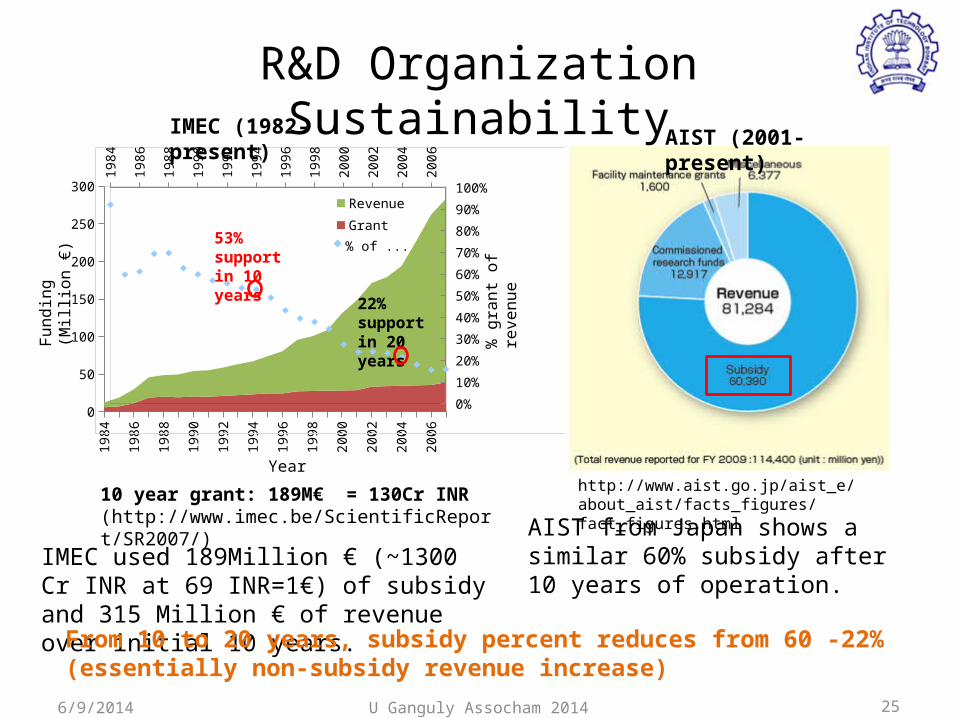
R&D Organization Sustainability
% g
rant
of r
even
ue
Fund
ing
(Mill
ion
€)
Year
53% support in 10 years
IMEC (1982- present) AIST (2001-present)
10 year grant: 189M€ = 130Cr INR (http://www.imec.be/ScientificReport/SR2007/)
http://www.aist.go.jp/aist_e/about_aist/facts_figures/fact_figures.html
IMEC used 189Million € (~1300 Cr INR at 69 INR=1€) of subsidy and 315 Million € of revenue over initial 10 years.
22% support in 20 years
AIST from Japan shows a similar 60% subsidy after 10 years of operation.
From 10 to 20 years, subsidy percent reduces from 60 -22% (essentially non-subsidy revenue increase)
6/9/2014
U Ganguly Assocham 2014
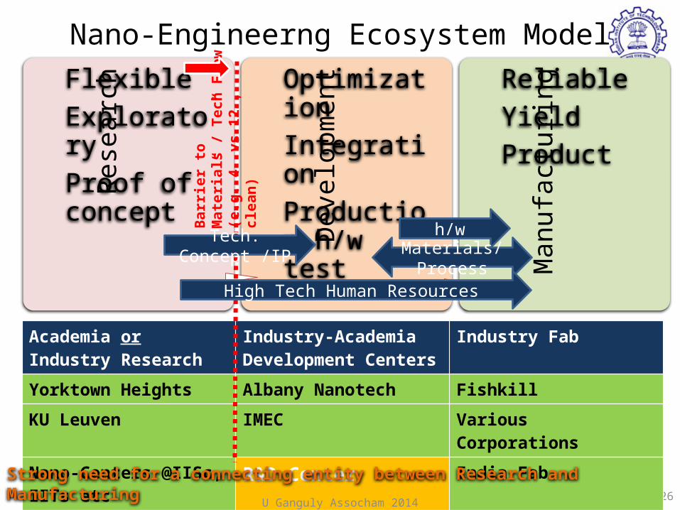
Nano-Engineerng Ecosystem Model
6/9/2014 P 26
Rese
arch Flexible
ExploratoryProof of concept
Dev
elop
men
t OptimizationIntegrationProduction h/w test
Man
ufac
turin
g Reliable YieldProduct
Academia or Industry Research
Industry-Academia Development Centers
Industry Fab
Yorktown Heights Albany Nanotech Fishkill
KU Leuven IMEC Various Corporations
Nano-Centers @IISc, IITs etc R&D Center India Fab
Strong need for a connecting entity between Research and Manufacturing
Barr
ier t
o M
ater
ials
/ T
ech
Flow
(e.g
. 4”
vs 1
2”, c
lean
)h/w
Tech. Concept /IPMaterials/Process
High Tech Human Resources
U Ganguly Assocham 2014 27
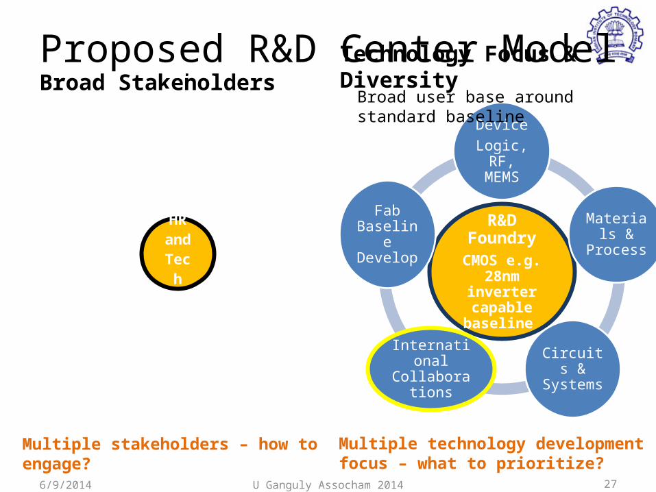
Proposed R&D Center ModelBroad Stakeholders
R&D Foundry
“Skilled HR and Tech for
Electronics ecosystem
”
Technology Focus & Diversity
R&D FoundryCMOS e.g.
28nm inverter capable baseline
DeviceLogic, RF,
MEMS
Materials & Process
Circuits & Systems
International Collaborations
Fab Baseline Develop
Broad user base around standard baseline
Multiple stakeholders – how to engage? Multiple technology development focus – what to prioritize?
6/9/2014

U Ganguly Assocham 2014 28
Board Representing Major
Stakeholders e.g.CEO, President
DeitYFab
DRDO/ISRO/DAEIndustry
Academia
6/9/2014
Organizational Structure
CEO, President
Fab &Industry Assignees Staff University
ResearchersTemporaryTemporary Permanent
CEO must have international experience in managing large R&D Labs/CentersStaff preferably have strong background in semiconductor industry or large R&D labs
R&D Center must be autonomously & professionally managed with vision from stakeholders
U Ganguly Assocham 2014 29
Prologue
SEMI and IESA industry forum to develop ecosystem consensus with GoI Leadership
6/9/2014
A globally time-tested R&D model needs to be implemented to support the bold vision of Indian semiconductor manufacturing and innovations