Embed Size (px)
Citation preview

Nanocrystallization of Steels by Severe Plastic Deformation
Minoru Umemoto
Department of Production Systems Engineering, Toyohashi University of Technology, Toyohashi 441-8580, Japan
The formation of nanocrystalline structure (NS) in steels by various severe plastic deformation processes, such as ball milling, a ball droptest, particle impact deformation and air blast shot peening are demonstrated. Layered or equiaxed nanograined region appeared near thespecimen surface and dislocated cell structured region appeared interior of specimens. These regions are separated with clearly definedboundaries. The deformation induced nanograined regions have the following common specific characteristics: 1) with grains smaller than100 nm and low dislocation density interior of grains, 2) extremely high hardness, 3) dissolution of cementite when it exist and 4) norecrystallization and slow grain growth by annealing. The deformation conditions to produce NS was discussed based on the available data inliteratures. It was suggested that the most important condition is to impose a strain larger than about 7. High strain rates, low deformationtemperature, multidirectional deformation, hydrostatic pressure are considered to be favorable conditions to produce NS. Introducing alloyingelements, precipitates and second phase also enhance nanocrystallization by suppressing recovery. The mechanisms of the formation of sharplydefined boundaries which separate nanograined structure region from dislocated cell structured region were discussed with respect to impurities,martensitic transformation and deformation. It was suggested several mechanisms may operate simultaneously in the formation of the clearboundaries.
(Received May 30, 2003; Accepted July 24, 2003)
Keywords: ball mill, ball drop, shot peening, nanocrystallne, microstructure, severe deformation, steel
1. Introduction
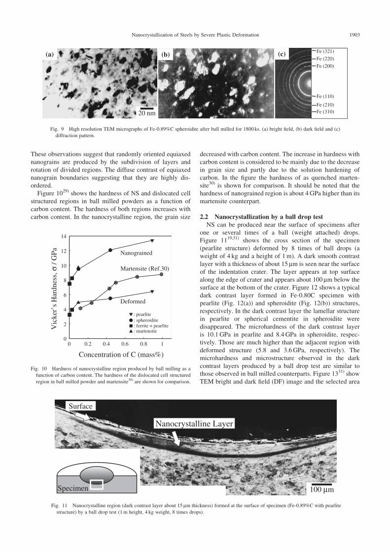
Large efforts have been devoted to refine grains ofmaterials since it enhances both strength and toughness.Figure 1 shows various processes to produce fine grainedmaterials of respective grain size ranges. In steel industry,thermomechanical control processing (TMCP),1) which con-sists of controlled hot rolling and accelerated cooling, hasbeen developed to produce fine grained materials with grainsize down to around 5 mm. In order to obtain the finer grainsup to 1 mm extended TMCP processes have been developed.2)
In such processes, diffusional transformation and/or recrys-tallization were mainly utilized to refine grains. In theconventional deformation processes such as rolling, drawing,extrusion, further refinement of grains to less than 1 mm isquite difficult since the final product size limits the maximumamount of strain introduced. To eliminate the strain limitarising from the materials size reduction, new deformationprocesses such as Equal channel angular pressing (ECAP)3–5)
or accumulative roll bonding (ARB)6,7) have been developed.
In ECAP process, pure shear deformation is repeatedlyimposed in materials without changing the cross-sectionaldimensions of the workpiece. Bulk rod-like specimens withsubmicron size grains has been obtained. In ARB, two piecesof sheet specimen were stacked and rolled to 50% reduction.The obtained roll-bonded sheet was cut into half length andrepeated such procedure by several cycles. Bulk sheet formspecimens with submicron grains has been obtained.
To obtain nanograined materials (grain size smaller than100 nm), various methods such as consolidation of ultrafinepowders,8) electron beam deposition,9) electrodeposition,10)
crystallization of amorphous phase,11) severe plastic defor-mation12–24) etc. have been developed. Figure 2 showsrepresentative severe plastic deformation processes to pro-duce nanocrystalline structure (NS): ball milling,12–15) highpressure torsion,16,17) sliding wear,18) a ball drop test,19,20)
ultrasonic shot peening21) and air blast shot peening.22–24)
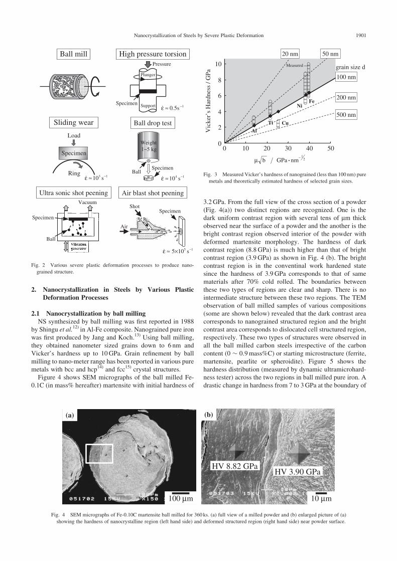
Figure 3 shows the reported Vicker’s hardness ranges ofvarious pure metals (includes specimens with a small amountof alloying elements) of nanometer sized grain (smaller than100 nm, called nanograin hereafter) produced by variousmethods.25,26) In the figure theoretically estimated hardnessof selected grain sizes are also shown. The theoreticalhardness value was calculated from Hall-Petch relationshipusing the equation HV ¼ HV0 þ 1:5�ðb=dÞ1=2 (where � isthe shear modulus, b the Bergers vector and d the graindiameter). As is seen, the reported hardness of Al, Ti, Ni andFe exceed the expected hardness of respective metals with100 nm grain size except Cu.
In the present review the microstructure evolutions insteels by ball milling, a ball drop test, particle impact test andair blast shot peening are presented. Focusing on iron andsteels, previous studies on the microstructural evolutionduring heavy deformation were reviewed. The amount ofstrain, strain rate and other favorable conditions to produceNS are discussed.
Grain size10 µm 1µm 100 nm 10 nm 1 nm
Nanocrystal
0.1 nm
Poly-crystal Amorphous
Consolidation of ultra fine particlesElectrodepositionCrystallization of amorphousSevere plastic deformation
Sintering of MA powderECAP, ARB
Super metal project, STX-21
TMCP
Conventional structural metals
Fe atomic diameter (0.248 nm)
Fig. 1 Production methods of fine grained materials for respective grain
size range.
Materials Transactions, Vol. 44, No. 10 (2003) pp. 1900 to 1911Special Issue on Nano-Hetero Structures in Advanced Metallic Materials#2003 The Japan Institute of MetalsOVERVIEW
2. Nanocrystallization in Steels by Various PlasticDeformation Processes
2.1 Nanocrystallization by ball millingNS synthesized by ball milling was first reported in 1988
by Shingu et al.12) in Al-Fe composite. Nanograined pure ironwas first produced by Jang and Koch.13) Using ball milling,they obtained nanometer sized grains down to 6 nm andVicker’s hardness up to 10GPa. Grain refinement by ballmilling to nano-meter range has been reported in various puremetals with bcc and hcp14) and fcc15) crystal structures.
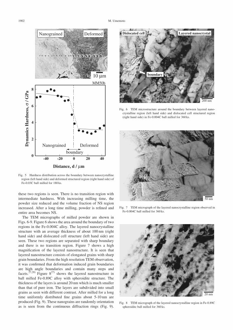
Figure 4 shows SEM micrographs of the ball milled Fe-0.1C (in mass% hereafter) martensite with initial hardness of
3.2GPa. From the full view of the cross section of a powder(Fig. 4(a)) two distinct regions are recognized. One is thedark uniform contrast region with several tens of mm thickobserved near the surface of a powder and the another is thebright contrast region observed interior of the powder withdeformed martensite morphology. The hardness of darkcontrast region (8.8GPa) is much higher than that of brightcontrast region (3.9GPa) as shown in Fig. 4 (b). The brightcontrast region is in the conventinal work hardened statesince the hardness of 3.9 GPa corresponds to that of samematerials after 70% cold rolled. The boundaries betweenthese two types of regions are clear and sharp. There is nointermediate structure between these two regions. The TEMobservation of ball milled samples of various compositions(some are shown below) revealed that the dark contrast areacorresponds to nanograined structured region and the brightcontrast area corresponds to dislocated cell structured region,respectively. These two types of structures were observed inall the ball milled carbon steels irrespective of the carboncontent (0 � 0:9mass%C) or starting microstructure (ferrite,martensite, pearlite or spheroidite). Figure 5 shows thehardness distribution (measured by dynamic ultramicrohard-ness tester) across the two regions in ball milled pure iron. Adrastic change in hardness from 7 to 3GPa at the boundary of
Ball mill
Vacuum
Specimen
Ball
Sliding wear
Specimen
Plunger
Support
Pressure
High pressure torsion
Air blast shot peening
Ball drop test
Air
Shot
Ring
Load
Ultra sonic shot peening
Specimen
Specimen
Ball
0.5s −1≈ε
3 s10 −1≈ε 4 s10 −1≈ε
5 s5×10 −1≈ε
Specimen
Weight1~5 kg
Fig. 2 Various severe plastic deformation processes to produce nano-
grained structure.
0
2
4
6
8
10
0 10 20 30 40 50
Ti
NiFe
21
GPa . nmbµ −
Vic
ker’
s H
ardn
ess
/ GPa
Measured
Cu
Al
50 nm20 nm
200 nm
500 nm
100 nm
grain size d
Fig. 3 Measured Vicker’s hardness of nanograined (less than 100 nm) pure
metals and theoretically estimated hardness of selected grain sizes.
HV 8.82 GPaHV 3.90 GPa
(a)
100 µm 10 µm
(b)
Fig. 4 SEM micrographs of Fe-0.10C martensite ball milled for 360 ks. (a) full view of a milled powder and (b) enlarged picture of (a)
showing the hardness of nanocrystalline region (left hand side) and deformed structured region (right hand side) near powder surface.
Nanocrystallization of Steels by Severe Plastic Deformation 1901
these two regions is seen. There is no transition region withintermediate hardness. With increasing milling time, thepowder size reduced and the volume fraction of NS regionincreased. After a long time milling, powder is refined andentire area becomes NS.
The TEM micrographs of milled powder are shown inFigs. 6-9. Figure 6 shows the area around the boundary of tworegions in the Fe-0.004C alloy. The layered nanocrystallinestructure with an average thickness of about 100 nm (righthand side) and dislocated cell structure (left hand side) areseen. These two regions are separated with sharp boundaryand there is no transition region. Figure 7 shows a highmagnification of the layered nanostructure. It is seen thatlayered nanostructure consists of elongated grains with sharpgrain boundaries. From the high resolution TEM observation,it was confirmed that deformation induced grain boundariesare high angle boundaries and contain many steps andfacets.27,28) Figure 827) shows the layered nanostructure inball milled Fe-0.89C alloy with spheroidite structure. Thethickness of the layers is around 20 nm which is much smallerthan that of pure iron. The layers are subdivided into smallgrains as seen with different contrast. After milled for a longtime uniformly distributed fine grains about 5-10 nm areproduced (Fig. 9). These nanograins are randomly orientationas is seen from the continuous diffraction rings (Fig. 9).
0
2
4
6
8
-40 -20 0 20 40
Distance, d / µm
Nanograined Deformed
MM50h
boundary
Dyn
amic
s H
ardn
ess,
σ /
GP
a
Nanograined
10 µm
Deformed
Fig. 5 Hardness distribution across the boundary between nanocrystalline
region (left hand side) and deformed structured region (right hand side) of
Fe-0.03C ball milled for 180 ks.
Layered nanocrystal
boundary
Dislocated cell
200 nm
Fig. 6 TEM microstructure around the boundary between layered nano-
crystalline region (left hand side) and dislocated cell structured region
(right hand side) in Fe-0.004C ball milled for 360 ks.
50 nm
Fig. 7 TEM micrograph of the layered nanocrystalline region observed in
Fe-0.004C ball milled for 360 ks.
20 nm
Fig. 8 TEM micrograph of the layered nanocrystalline region in Fe-0.89C
spheroidite ball milled for 360 ks.
1902 M. Umemoto
These observations suggest that randomly oriented equiaxednanograins are produced by the subdivision of layers androtation of divided regions. The diffuse contrast of equiaxednanograin boundaries suggesting that they are highly dis-ordered.
Figure 1029) shows the hardness of NS and dislocated cellstructured regions in ball milled powders as a function ofcarbon content. The hardness of both regions increases withcarbon content. In the nanocrystalline region, the grain size
decreased with carbon content. The increase in hardness withcarbon content is considered to be mainly due to the decreasein grain size and partly due to the solution hardening ofcarbon. In the figure the hardness of as quenched marten-site30) is shown for comparison. It should be noted that thehardness of nanograined region is about 4GPa higher than itsmartensite counterpart.
2.2 Nanocrystallization by a ball drop testNS can be produced near the surface of specimens after
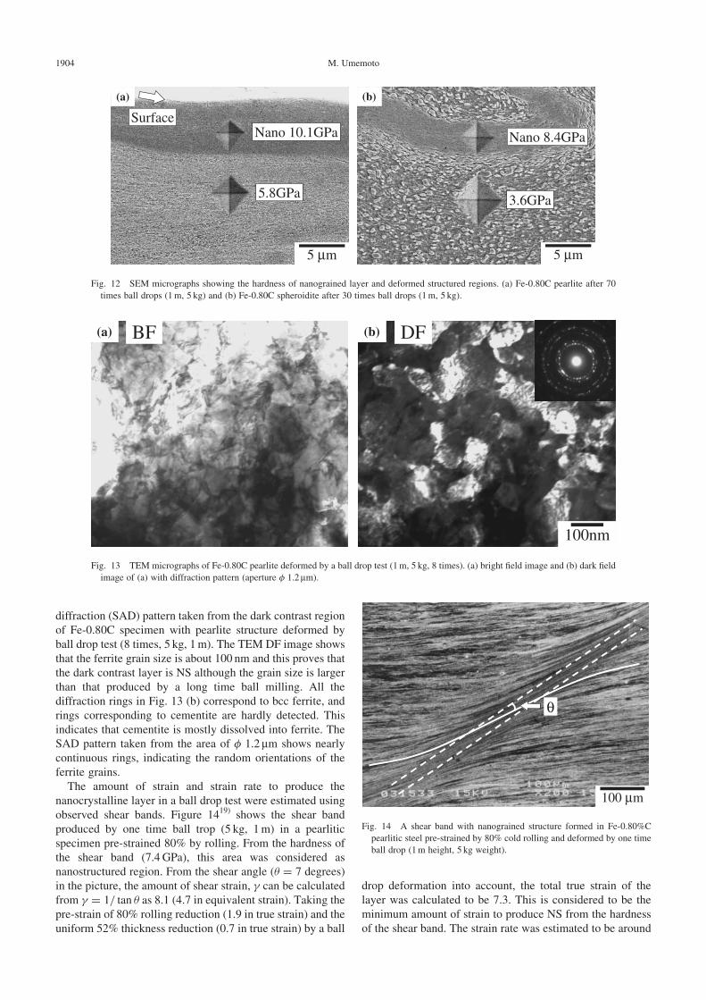
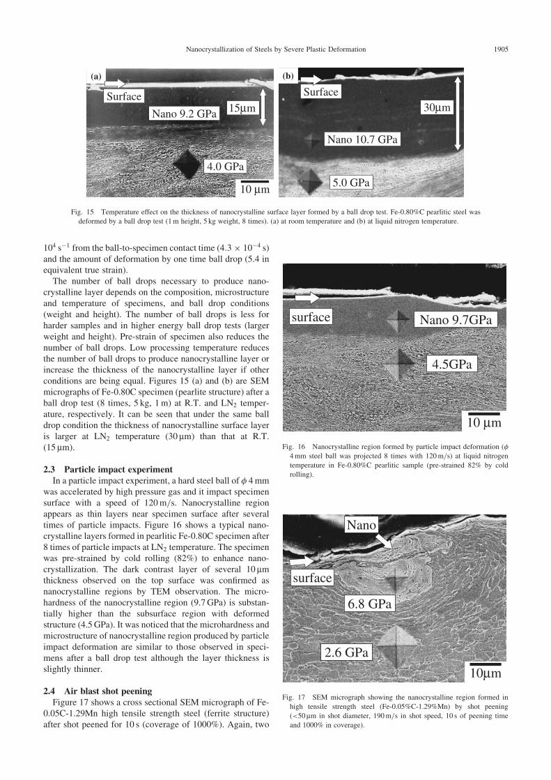
one or several times of a ball (weight attached) drops.Figure 1119,31) shows the cross section of the specimen(pearlite structure) deformed by 8 times of ball drops (aweight of 4 kg and a height of 1m). A dark smooth contrastlayer with a thickness of about 15 mm is seen near the surfaceof the indentation crater. The layer appears at top surfacealong the edge of crater and appears about 100 mm below thesurface at the bottom of the crater. Figure 12 shows a typicaldark contrast layer formed in Fe-0.80C specimen withpearlite (Fig. 12(a)) and spheroidite (Fig. 12(b)) structures,respectively. In the dark contrast layer the lamellar structurein pearlite or spherical cementite in spheroidite weredisappeared. The microhardness of the dark contrast layeris 10.1GPa in pearlite and 8.4GPa in spheroidite, respec-tively. Those are much higher than the adjacent region withdeformed structure (5.8 and 3.6GPa, respectively). Themicrohardness and microstructure observed in the darkcontrast layers produced by a ball drop test are similar tothose observed in ball milled counterparts. Figure 1331) showTEM bright and dark field (DF) image and the selected area
Fe (110)
Fe (210)Fe (310)
Fe (200)
Fe (220)
Fe (321)(a) (b)
20 nm
(c)
Fig. 9 High resolution TEM micrographs of Fe-0.89%C spheroidite after ball milled for 1800 ks. (a) bright field, (b) dark field and (c)
diffraction pattern.
0
2
4
6
8
10
12
14
0 0.2 0.4 0.6 0.8 1
Concentration of C (mass%)
Nanograined
Deformed
Vic
ker’
s H
ardn
ess,
σ /
GPa
Martensite (Ref.30)
: ferrite + pearlite: martensite
: pearlite: spheroidite
Fig. 10 Hardness of nanocrystalline region produced by ball milling as a
function of carbon content. The hardness of the dislocated cell structured
region in ball milled powder and martensite30) are shown for comparison.
Surface
Specimen
Nanocrystalline Layer
100 µm
Fig. 11 Nanocrystalline region (dark contrast layer about 15 mm thickness) formed at the surface of specimen (Fe-0.89%C with pearlite
structure) by a ball drop test (1m height, 4 kg weight, 8 times drops).
Nanocrystallization of Steels by Severe Plastic Deformation 1903
diffraction (SAD) pattern taken from the dark contrast regionof Fe-0.80C specimen with pearlite structure deformed byball drop test (8 times, 5 kg, 1m). The TEM DF image showsthat the ferrite grain size is about 100 nm and this proves thatthe dark contrast layer is NS although the grain size is largerthan that produced by a long time ball milling. All thediffraction rings in Fig. 13 (b) correspond to bcc ferrite, andrings corresponding to cementite are hardly detected. Thisindicates that cementite is mostly dissolved into ferrite. TheSAD pattern taken from the area of � 1.2 mm shows nearlycontinuous rings, indicating the random orientations of theferrite grains.
The amount of strain and strain rate to produce thenanocrystalline layer in a ball drop test were estimated usingobserved shear bands. Figure 1419) shows the shear bandproduced by one time ball trop (5 kg, 1m) in a pearliticspecimen pre-strained 80% by rolling. From the hardness ofthe shear band (7.4 GPa), this area was considered asnanostructured region. From the shear angle (� ¼ 7 degrees)in the picture, the amount of shear strain, � can be calculatedfrom � ¼ 1= tan � as 8.1 (4.7 in equivalent strain). Taking thepre-strain of 80% rolling reduction (1.9 in true strain) and theuniform 52% thickness reduction (0.7 in true strain) by a ball
drop deformation into account, the total true strain of thelayer was calculated to be 7.3. This is considered to be theminimum amount of strain to produce NS from the hardnessof the shear band. The strain rate was estimated to be around
3.6GPa
Nano 8.4GPaNano 10.1GPa
5.8GPa
Surface
(a) (b)
5 µm 5 µm
Fig. 12 SEM micrographs showing the hardness of nanograined layer and deformed structured regions. (a) Fe-0.80C pearlite after 70
times ball drops (1m, 5 kg) and (b) Fe-0.80C spheroidite after 30 times ball drops (1m, 5 kg).
DFBF
100nm
(a) (b)
Fig. 13 TEM micrographs of Fe-0.80C pearlite deformed by a ball drop test (1m, 5 kg, 8 times). (a) bright field image and (b) dark field
image of (a) with diffraction pattern (aperture � 1.2mm).
θ
100 µm
Fig. 14 A shear band with nanograined structure formed in Fe-0.80%C
pearlitic steel pre-strained by 80% cold rolling and deformed by one time
ball drop (1m height, 5 kg weight).
1904 M. Umemoto
104 s�1 from the ball-to-specimen contact time (4:3� 10�4 s)and the amount of deformation by one time ball drop (5.4 inequivalent true strain).
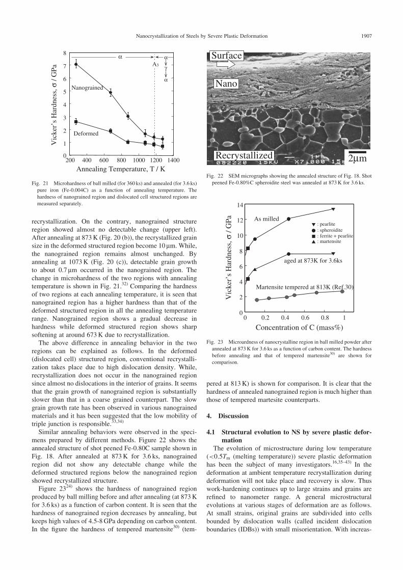
The number of ball drops necessary to produce nano-crystalline layer depends on the composition, microstructureand temperature of specimens, and ball drop conditions(weight and height). The number of ball drops is less forharder samples and in higher energy ball drop tests (largerweight and height). Pre-strain of specimen also reduces thenumber of ball drops. Low processing temperature reducesthe number of ball drops to produce nanocrystalline layer orincrease the thickness of the nanocrystalline layer if otherconditions are being equal. Figures 15 (a) and (b) are SEMmicrographs of Fe-0.80C specimen (pearlite structure) after aball drop test (8 times, 5 kg, 1m) at R.T. and LN2 temper-ature, respectively. It can be seen that under the same balldrop condition the thickness of nanocrystalline surface layeris larger at LN2 temperature (30 mm) than that at R.T.(15 mm).
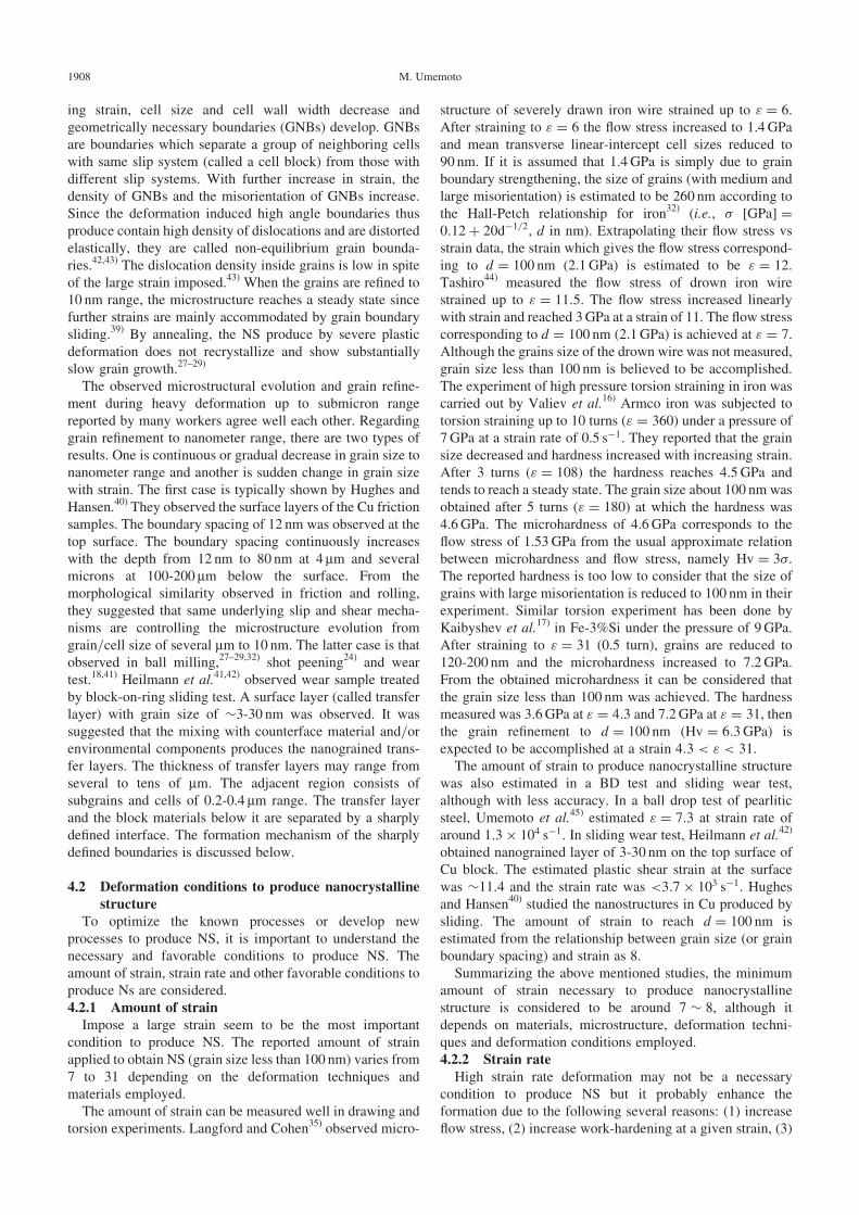
2.3 Particle impact experimentIn a particle impact experiment, a hard steel ball of � 4mm
was accelerated by high pressure gas and it impact specimensurface with a speed of 120m/s. Nanocrystalline regionappears as thin layers near specimen surface after severaltimes of particle impacts. Figure 16 shows a typical nano-crystalline layers formed in pearlitic Fe-0.80C specimen after8 times of particle impacts at LN2 temperature. The specimenwas pre-strained by cold rolling (82%) to enhance nano-crystallization. The dark contrast layer of several 10 mmthickness observed on the top surface was confirmed asnanocrystalline regions by TEM observation. The micro-hardness of the nanocrystalline region (9.7GPa) is substan-tially higher than the subsurface region with deformedstructure (4.5GPa). It was noticed that the microhardness andmicrostructure of nanocrystalline region produced by particleimpact deformation are similar to those observed in speci-mens after a ball drop test although the layer thickness isslightly thinner.
2.4 Air blast shot peeningFigure 17 shows a cross sectional SEM micrograph of Fe-
0.05C-1.29Mn high tensile strength steel (ferrite structure)after shot peened for 10 s (coverage of 1000%). Again, two
Surface 30µm
Nano 10.7 GPa
5.0 GPa
15µm
4.0 GPa
Nano 9.2 GPa
10 µm
(a)
Surface
(b)
Fig. 15 Temperature effect on the thickness of nanocrystalline surface layer formed by a ball drop test. Fe-0.80%C pearlitic steel was
deformed by a ball drop test (1m height, 5 kg weight, 8 times). (a) at room temperature and (b) at liquid nitrogen temperature.
Nano 9.7GPa
4.5GPa
surface
10 µm
Fig. 16 Nanocrystalline region formed by particle impact deformation (�
4mm steel ball was projected 8 times with 120m/s) at liquid nitrogen
temperature in Fe-0.80%C pearlitic sample (pre-strained 82% by cold
rolling).
6.8 GPa
2.6 GPa
surface
Nano
10µm
Fig. 17 SEM micrograph showing the nanocrystalline region formed in
high tensile strength steel (Fe-0.05%C-1.29%Mn) by shot peening
(<50mm in shot diameter, 190m/s in shot speed, 10 s of peening time
and 1000% in coverage).
Nanocrystallization of Steels by Severe Plastic Deformation 1905

distinctive regions can be seen. One is the smooth contrast(nanocrystalline) region near surface with the hardness of6.8GPa. Another is the deformed structured region observedat subsurface with the hardness of 2.6GPa. Figure 18 showscross section of near surface area of shot peened Fe-0.8Cspecimen (spheroidite structure pre-strained 84% by coldrolling) after shot peening. Nanocrystalline layer with 5 mmthickness is produced at the top surface. Before shot peening,the spherical cementite particles with diameter about 0.5 mmwere uniformly distributed in the ferrite matrix. After shot
peening, cementite particles are not visible in the nano-crystalline surface layer. This indicating that the dissolutionof cementite takes place in the nanocrystalline layer similarto that observed in ball milled or ball dropped specimens.Figure 19(a) shows nanocrystalline region formed in Fe-3.29Si specimen by 10 s of shot peening (coverage of1000%). The sharp boundaries are seen between the topsurface nanocrystalline layer and subsurface deformedstructured region. Figure 19(b) is the TEM dark field (DF)image and selected area diffraction (SAD) pattern of the topsurface region of Fe-3.29Si specimen shot peened for 60 s(coverage 6000%). The DF image shows that the ferrite grainsize is less than 20 nm, and the SAD pattern indicates that theferrite grains are randomly orientated.
The production of nanocrystalline surface layer by air blastshot peening has considerable industrial importance since airblast shot peening is a popular process in industries and it canproduce nanostructured surface layer with a high productiv-ity. Industrial application of this new technology is expectedespecially to upgrade the traditional engineering materials.
3. Annealing Behavior of Nanocrystalline Region
The annealing behaviors of nanograined region are quitedifferent from those of the deformed structured region.Figure 20 shows the microstructural change with annealingtemperature (annealed for 3.6 ks) in ball milled pure iron (Fe-0.004C). By annealed at 673K (Fig. 20 (a)), the deformedstructured region (lower right) becomes equiaxed grainedstructure with an average grain size of about 0.5 mm by
2 µm
Surface Nano
Deformed
Fig. 18 SEM micrographs showing the nanograined region formed in Fe-
0.80%C steel with spheroidite structure (84% cold rolled before shot
peening) by shot peening (<50mm in shot diameter, 190m/s in shot speed,
10 s in peening time and 1000% in coverage).
Surface
Nano
2 µm 100 nm
(a) (b)
Fig. 19 Micrographs of shot peened (<50 mm in shot diameter, 190m/s in shot speed) Fe-3.29Si steel. (a) SEM after peened 10 s (1000%
in coverage) and (b) TEM (dark field) after peened for 60 s (6000% in coverage). The aperture size of diffraction was � 1.2mm.
(a) 673 K
Nano
(b) 873 K (c) 1073 K
2µm
Fig. 20 SEM micrographs of ball milled (for 360 ks) and annealed (for 3.6 ks) pure iron (Fe-0.004C). (a) at 673K, (b) at 873K and (c) at
1073K.
1906 M. Umemoto
recrystallization. On the contrary, nanograined structureregion showed almost no detectable change (upper left).After annealing at 873K (Fig. 20 (b)), the recrystallized grainsize in the deformed structured region become 10 mm. While,the nanograined region remains almost unchanged. Byannealing at 1073K (Fig. 20 (c)), detectable grain growthto about 0.7 mm occurred in the nanograined region. Thechange in microhardness of the two regions with annealingtemperature is shown in Fig. 21.32) Comparing the hardnessof two regions at each annealing temperature, it is seen thatnanograined region has a higher hardness than that of thedeformed structured region in all the annealing temperaturerange. Nanograined region shows a gradual decrease inhardness while deformed structured region shows sharpsoftening at around 673K due to recrystallization.
The above difference in annealing behavior in the tworegions can be explained as follows. In the deformed(dislocated cell) structured region, conventional recrystalli-zation takes place due to high dislocation density. While,recrystallization does not occur in the nanograined regionsince almost no dislocations in the interior of grains. It seemsthat the grain growth of nanograined region is substantiallyslower than that in a coarse grained counterpart. The slowgrain growth rate has been observed in various nanograinedmaterials and it has been suggested that the low mobility oftriple junction is responsible.33,34)
Similar annealing behaviors were observed in the speci-mens prepared by different methods. Figure 22 shows theannealed structure of shot peened Fe-0.80C sample shown inFig. 18. After annealed at 873K for 3.6 ks, nanograinedregion did not show any detectable change while thedeformed structured regions below the nanograined regionshowed recrystallized structure.
Figure 2324) shows the hardness of nanograined regionproduced by ball milling before and after annealing (at 873Kfor 3.6 ks) as a function of carbon content. It is seen that thehardness of nanograined region decreases by annealing, butkeeps high values of 4.5-8GPa depending on carbon content.In the figure the hardness of tempered martensite30) (tem-
pered at 813K) is shown for comparison. It is clear that thehardness of annealed nanograined region is much higher thanthose of tempered martesite counterparts.
4. Discussion
4.1 Structural evolution to NS by severe plastic defor-mation
The evolution of microstructure during low temperature(<0:5Tm (melting temperature)) severe plastic deformationhas been the subject of many investigators.16,35–43) In thedeformation at ambient temperature recrystallization duringdeformation will not take place and recovery is slow. Thuswork-hardening continues up to large strains and grains arerefined to nanometer range. A general microstructuralevolutions at various stages of deformation are as follows.At small strains, original grains are subdivided into cellsbounded by dislocation walls (called incident dislocationboundaries (IDBs)) with small misorientation. With increas-
0
1
2
3
4
5
6
7
8
200 400 600 800 1000 1200 1400
Annealing Temperature, T / K
Nanograined
Deformed
A3
α
α
α
γ
Vic
ker’
s H
ardn
ess,
σ /
GPa
Fig. 21 Microhardness of ball milled (for 360 ks) and annealed (for 3.6 ks)
pure iron (Fe-0.004C) as a function of annealing temperature. The
hardness of nanograined region and dislocated cell structured regions are
measured separately.
2µm
Surface
Recrystallized
Nano
Fig. 22 SEM micrographs showing the annealed structure of Fig. 18. Shot
peened Fe-0.80%C spheroidite steel was annealed at 873K for 3.6 ks.
0
2
4
6
8
10
12
14
0 0.2 0.4 0.6 0.8 1
Concentration of C (mass%)
As milled
Martensite tempered at 813K (Ref.30)
aged at 873K for 3.6ks
: ferrite + pearlite: martensite
: pearlite: spheroidite
Vic
ker’
s H
ardn
ess,
σ /
GPa
Fig. 23 Microardness of nanocrystalline region in ball milled powder after
annealed at 873K for 3.6 ks as a function of carbon content. The hardness
before annealing and that of tempered martensite30) are shown for
comparison.
Nanocrystallization of Steels by Severe Plastic Deformation 1907
ing strain, cell size and cell wall width decrease andgeometrically necessary boundaries (GNBs) develop. GNBsare boundaries which separate a group of neighboring cellswith same slip system (called a cell block) from those withdifferent slip systems. With further increase in strain, thedensity of GNBs and the misorientation of GNBs increase.Since the deformation induced high angle boundaries thusproduce contain high density of dislocations and are distortedelastically, they are called non-equilibrium grain bounda-ries.42,43) The dislocation density inside grains is low in spiteof the large strain imposed.43) When the grains are refined to10 nm range, the microstructure reaches a steady state sincefurther strains are mainly accommodated by grain boundarysliding.39) By annealing, the NS produce by severe plasticdeformation does not recrystallize and show substantiallyslow grain growth.27–29)
The observed microstructural evolution and grain refine-ment during heavy deformation up to submicron rangereported by many workers agree well each other. Regardinggrain refinement to nanometer range, there are two types ofresults. One is continuous or gradual decrease in grain size tonanometer range and another is sudden change in grain sizewith strain. The first case is typically shown by Hughes andHansen.40) They observed the surface layers of the Cu frictionsamples. The boundary spacing of 12 nm was observed at thetop surface. The boundary spacing continuously increaseswith the depth from 12 nm to 80 nm at 4 mm and severalmicrons at 100-200 mm below the surface. From themorphological similarity observed in friction and rolling,they suggested that same underlying slip and shear mecha-nisms are controlling the microstructure evolution fromgrain/cell size of several mm to 10 nm. The latter case is thatobserved in ball milling,27–29,32) shot peening24) and weartest.18,41) Heilmann et al.41,42) observed wear sample treatedby block-on-ring sliding test. A surface layer (called transferlayer) with grain size of �3-30 nm was observed. It wassuggested that the mixing with counterface material and/orenvironmental components produces the nanograined trans-fer layers. The thickness of transfer layers may range fromseveral to tens of mm. The adjacent region consists ofsubgrains and cells of 0.2-0.4 mm range. The transfer layerand the block materials below it are separated by a sharplydefined interface. The formation mechanism of the sharplydefined boundaries is discussed below.
4.2 Deformation conditions to produce nanocrystallinestructure
To optimize the known processes or develop newprocesses to produce NS, it is important to understand thenecessary and favorable conditions to produce NS. Theamount of strain, strain rate and other favorable conditions toproduce Ns are considered.4.2.1 Amount of strain
Impose a large strain seem to be the most importantcondition to produce NS. The reported amount of strainapplied to obtain NS (grain size less than 100 nm) varies from7 to 31 depending on the deformation techniques andmaterials employed.
The amount of strain can be measured well in drawing andtorsion experiments. Langford and Cohen35) observed micro-
structure of severely drawn iron wire strained up to " ¼ 6.After straining to " ¼ 6 the flow stress increased to 1.4GPaand mean transverse linear-intercept cell sizes reduced to90 nm. If it is assumed that 1.4 GPa is simply due to grainboundary strengthening, the size of grains (with medium andlarge misorientation) is estimated to be 260 nm according tothe Hall-Petch relationship for iron32) (i.e., � ½GPa� ¼0:12þ 20d�1=2, d in nm). Extrapolating their flow stress vsstrain data, the strain which gives the flow stress correspond-ing to d ¼ 100 nm (2.1GPa) is estimated to be " ¼ 12.Tashiro44) measured the flow stress of drown iron wirestrained up to " ¼ 11:5. The flow stress increased linearlywith strain and reached 3GPa at a strain of 11. The flow stresscorresponding to d ¼ 100 nm (2.1GPa) is achieved at " ¼ 7.Although the grains size of the drown wire was not measured,grain size less than 100 nm is believed to be accomplished.The experiment of high pressure torsion straining in iron wascarried out by Valiev et al.16) Armco iron was subjected totorsion straining up to 10 turns (" ¼ 360) under a pressure of7GPa at a strain rate of 0.5 s�1. They reported that the grainsize decreased and hardness increased with increasing strain.After 3 turns (" ¼ 108) the hardness reaches 4.5 GPa andtends to reach a steady state. The grain size about 100 nm wasobtained after 5 turns (" ¼ 180) at which the hardness was4.6GPa. The microhardness of 4.6 GPa corresponds to theflow stress of 1.53GPa from the usual approximate relationbetween microhardness and flow stress, namely Hv ¼ 3�.The reported hardness is too low to consider that the size ofgrains with large misorientation is reduced to 100 nm in theirexperiment. Similar torsion experiment has been done byKaibyshev et al.17) in Fe-3%Si under the pressure of 9GPa.After straining to " ¼ 31 (0.5 turn), grains are reduced to120-200 nm and the microhardness increased to 7.2GPa.From the obtained microhardness it can be considered thatthe grain size less than 100 nm was achieved. The hardnessmeasured was 3.6GPa at " ¼ 4:3 and 7.2GPa at " ¼ 31, thenthe grain refinement to d ¼ 100 nm (Hv ¼ 6:3GPa) isexpected to be accomplished at a strain 4:3 < " < 31.
The amount of strain to produce nanocrystalline structurewas also estimated in a BD test and sliding wear test,although with less accuracy. In a ball drop test of pearliticsteel, Umemoto et al.45) estimated " ¼ 7:3 at strain rate ofaround 1:3� 104 s�1. In sliding wear test, Heilmann et al.42)
obtained nanograined layer of 3-30 nm on the top surface ofCu block. The estimated plastic shear strain at the surfacewas �11:4 and the strain rate was <3:7� 103 s�1. Hughesand Hansen40) studied the nanostructures in Cu produced bysliding. The amount of strain to reach d ¼ 100 nm isestimated from the relationship between grain size (or grainboundary spacing) and strain as 8.
Summarizing the above mentioned studies, the minimumamount of strain necessary to produce nanocrystallinestructure is considered to be around 7 � 8, although itdepends on materials, microstructure, deformation techni-ques and deformation conditions employed.4.2.2 Strain rate
High strain rate deformation may not be a necessarycondition to produce NS but it probably enhance theformation due to the following several reasons: (1) increaseflow stress, (2) increase work-hardening at a given strain, (3)
1908 M. Umemoto
increase dislocation multiplication rate, and (4) promotelattice rotation and increase misorientation angle.
It has been well known that flow stress of metals increasewith strain rate.46) Higher flow stresses activate a largernumber of slip systems and promote grain subdivision andsubgrain rotation. Greater hardening has been observed inmetals strained at higher strain rates when compared at equalstrain. The iron samples subjected to high-intensity shockwaves of explosive origin (strain rate �106 s�1) showedmuch greater hardening than those deformed by rolling.47)
Thus it is expected that high strain rate deformation reducethe necessary amount of strain to produce NS. High strainrate deformation promote smaller cells or subgrains due tohigher dislocation multiplication rate and hence higherdislocation density than those deformed at low strain rates.The rotation of cells or grains is induced by the deformationof different slip systems in adjacent cells or grains. Since highstrain rate deformation activate more slip systems due to highflow stress, high strain rates are favorable to obtain randomlyoriented fine grains with large misorientation.
As the strain rate is increased the deformation tends moreand more towards an adiabatic state. The generated heat risethe temperature of sample and accelerates recovery and graingrowth. In an extreme case the increase in strain rate resultsin the increase in grain size.48) Thus to obtain grainrefinement by high strain rate deformation, care should betaken for cooling during and post deformation so that thetemperature of the specimen will not rise so much.4.2.3 Other deformation factors
Other favorable conditions for the formation of NS areconsidered as follows; (1) low temperature deformation, (2)hydrostatic pressure, (3) repetitive or cyclic deformation, (4)multidirectional deformation, (5) impurities, alloying ele-ments and second phase.
The suppression of recovery by preventing dislocationmotion favors the formation of NS. Low deformationtemperature and hydrostatic pressure slow down self-diffu-sion and, consequently, delay recovery kinetics. Applying alarge accumulative strain by cyclic or repetitive deformationwith a small strain at each time is effective to suppressrecovery since specimens are cooled during each straininterval. Multidirectional deformation activates multi slipsystems and increases dislocation interaction frequencieswhich leads to the development of fine cells. Impurities,alloying elements, precipitates and second phase disturbdislocation motion and suppress recovery.
4.3 Clear boundaries separate nanograined regionClear boundaries which separate nanograined region from
deformed structured region shown typically in Fig. 4 werecommonly observed in ball milling, a ball drop test, particleimpact experiment and shot peening. However, in most of theprevious studies, clear boundaries have not been observedand the refinement of cells or grains by deformation has beenconsidered to be a continuous process. The possible causes ofthe formation of sharply defined boundaries are; (1) impur-ities, (2) martensitic transformation, (3) unique deformationmode, (4) common phenomena in deformation. The effect ofimpurity has been discussed regarding the sharp boundariesobserved in ball milled powder.32) In ball milling contami-
nation from balls, vials and environmental gases occurs. Thepowder surface with higher impurity concentration becomesNS and interior of powder with lower impurity contentremains as deformed cell structure and clear boundariesappear between them. Impurities retards dislocation motionand certain elements segregate to grain boundaries, reducegrain boundary energy and promote nanocrystallization.However, clear boundaries were observed in specimenstreated by a ball drop test or shot peening where contami-nation is hard to occur. Thus it is considered that impurityalone cannot be a reason of the clear boundaries although itmight help. The second possible reason of the formation ofclear boundaries is martensitic transformation. This idea isthat nanograined region formed by martensitic transforma-tion is separated with clear boundary from the deformedstructured region without martensitic transformation. Whenspecimens received large strains at high strain rates, thetemperature of the specimen rise substantially. If the temper-ature rises above A1 or A3 point, the transformation toaustenite phase can occurs. During unloading, the temper-ature of austenite area decreases rapidly and transforms tomartensite. The martensitic transformation during cooling ofthe adiabatically deformed materials have been observed onthe rail surface and called ‘‘white etching layer’’.49) However,the nanograined regions produced in carbon steels exhibitmuch higher hardness than that of martensite with samecarbon content. Furthermore, as observed in a ball drop testwhen specimens are deformed at liquid nitrogen temperature,the nanograined layer thickness become larger than thatproduced at room temperature. Nanograined region alsoforms in Fe-3%Si alloy where the bcc phase is stable up to itsmelting temperature. From those reasons, it is hard to acceptthat thermally induced fcc to bcc martensitic transformationis responsible for the observed clear boundaries. Anotherpossible martensitic transformation is bcc to hcp trans-formation by hydrostatic pressure. In iron, bcc to hcptransformation takes place around 11.0-11.5GPa at roomtemperature.50) According to the Hertzian elastic contacttheory,51) when a spherical particle impact a semi-infinitespecimen with the speed of 100m/s, the maximum pressureis 15GPa. Thus in steels pressure induced martensitictransformation from bcc to hcp can occur when a highvelocity particle impact a specimen. During unloading, thehcp structure re-transform to bcc martensitically. Althoughmartensitic transformation alone cannot produce nanocrys-tallization but martensitic transformation produces irrever-sible lattice defects and reduce the amount of strain to reachnanocrystalline state. The unique deformation mode can beanother reason of clear boundaries. In ball milling, a ball droptest, particle impact deformation or shot peening, the strain ishighly concentrated near specimen surface. The amount ofstrain and strain rate is a strong function of depth from thesurface. Thus it can be considered that the clear boundarymay corresponds to drastic change in the strain or strain rate.However, strain or strain rate in a material changescontinuously with distance and hard to consider they changesuch abruptly. Furthermore various amount of strains aregiven at various strain rates in the processes studied butintermediate structure between nanocrystalline and dislocat-ed cell structures has never been observed. The last proposed
Nanocrystallization of Steels by Severe Plastic Deformation 1909

idea is to consider that the sharp transition from dislocatedcell to nanocrystalline structure is common phenomena indeformation and this occurs irrespective of materials or modeof deformation. However, gradual change in grain size tonanometer range has been observed40) and it is hard to acceptthat sharp change is a common behavior of deformedmaterial. From the above discussion on the formationmechanisms of the clear boundaries between nanograinedand dislocated cell structures, it is suggested that severalreasons may contribute simultaneously. The real mechanismis still not clear and further investigations are needed.
5. Summary and Conclusions
In the present paper, the formation of nanograinedstructure by various severe plastic deformation were dem-onstrated. The general microstructural changes during severedeformation observed were reviewed. The conditions toproduce nanograined structure were discussed. The maincontents are summarized as follows.(1) In ball milling, nanograined structure was obtained insteels irrespective of the carbon content and starting micro-structure. The nanograined regions appear near the surface ofpowder and are separated from the interior deformedstructured region with sharp boundaries. The hardness ofnanograined region is extremely high and increases withcarbon content from 7 to 13GPa. The cementite (eitherlamellar or spherical) dissolves completely by ball millingwhen the nanocrystallization of ferrite matrix starts.(2) In a ball drop test and particle impact deformation, similarnanograined structure was obtained in the surface layer afterseveral times of impact. Deformation at liquid nitrogentemperature enhanced the formation of nanograined region.(3) In air blast shot peening, nanograined structure isproduced when larger coverage (>1000%) and higher shotspeed (>100m/s) than conventional operation are applied.(4) By annealing, nanograined structured region showedsubstantially slow grain growth without recrystallization.(5) The microstructure change from dislocated cell tonanograined structure during severe plastic deformationoccurs either gradually or discontinuously depending on aprocess employed.(6) To produce nanograined structure by deformation, themost important condition is to impose a large strain (largerthan about 7). High strain rates, low temperature deforma-tion, multidirectional deformation, hydrostatic pressure areconsidered to be favorable conditions to produce nanograinedstructure.(7) The mechanisms of the formation of sharply definedboundaries which separate nanograined region from dislo-cated cell structured region were discussed with respect toimpurities, martensitic transformation and deformationmode. It was suggested several mechanisms may operatesimultaneously in the formation of the clear boundaries.
Acknowledgements
This work is partly supported by the Grant-in-Aid by theJapan Society for the Promotion of Science. The authorthanks Dr. K. Tsuchiya, Dr. Y. Todaka for their involvement.
REFERENCES
1) I. Tamura, H. Sekine, T. Tanaka and C. Ouchi: Thermomechanical
Processing of High-strength Low-alloy Steels, (Butterworths, 1988).
2) M. Niikura, Y. Hagiwara, K. Nagai, K. Tsuzaki and S. Takaki: Proc. of
Int. Symp. on Ultrafine Grained Steels, (The Iron and Steel Inst. of
Japan, 2001) 26-33.
3) V. M. Segal, V. I. Reznikov, A. D. Drobyshevskiy and V. I. Kopylov:
Russ. Metall. 1 (1981) 99-105.
4) R. Z. Valiev, N. A. Krasilnikov and N. K. Tsenev: Mater. Sci. Eng. A
137 (1991) 35-40.
5) R. Z. Valiev, A. V. Korznikov and R. R. Mulyukov: Phys. Met. Metall.
73 (1992) 373-383.
6) Y. Saito, N. Tsuji, H. Utsunomiya, T. Sakai and R. G. Hong: Scr.
Mater. 39 (1998) 1221-1227.
7) Y. Saito, H. Utsunomiya, N. Tsuji and T. Sakai: Acta Mater. 47 (1999)
579-583.
8) H. Gleiter: 2nd Riso Int. Symp. Metall. and Mat. Sci., eds. N. Hansen,
A. Horsewell and H. Lilholt (Riso National Laboratory, Denmark,
1981) 15-21.
9) L. Lu, M. L. Sui and K. Lu: Science 287 (2000) 1463-1466.
10) G. Plumbo, S. J. Thorpe and K. T. Aust: Scr. Metall. Mater. 24 (1990)
1347-1350.
11) Y. Yoshizawa, S. Oguma and K. J. Yamaguchi: J. Appl. Phys. 64
(1988) 6044-6046.
12) P. H. Shingu, B. Huang, S. R. Nishitani and S. Nasu: Proc. of JIMIS-5,
Non-Equilibrium Solid Phases of Metals and Alloys 29 (1988) 3-10.
13) J. S. C. Jang and C. C. Koch: Sri. Metal. 24 (1990) 1599-1604.
14) H. J. Fecht, E. Hellstern, Z. Fu and W. L. Johnson: Metall. Trans. 21A
(1990) 2333-2337.
15) J. Eckert, J. C. Holzer, C. E. Krill, III and W. L. Johnson: J. Mater. Res.
7 (1992) 1751-1761.
16) R. Z. Valiev, Y. V. Ivanisenko, E. F. Rauch and B. Baudelet: Acta
Mater. 44 (1996) 4705-4712.
17) R. Kaibyshev, I. Kazakulov, T. Sakai and A. Belyakov: Proc. of Int.
Symp. on Ultrafine Grained Steels, (The Iron and Steel Inst. of Japan,
2001) 152-155.
18) P. Heilmann, W. A. T. Clark and D. A. Rigney: Acta Metall. 31 (1983)
1293-1305.
19) M. Umemoto, B. Haung, K. Tsuchiya and N. Suzuki: Scr. Mater. 46
(2002) 383-388.
20) M. Umemoto, X. J. Hao, T. Yasuda and K. Tsuchiya: Mater. Trans. 43
(2002) 2536-2542.
21) N. R. Tao, M. L. Sui, J. Ku and K. Lu: NanoStructured Mater. 11 (1999)
433-440.
22) I. Altenberger, B. Scholtes, U. Martin and H. Oettel: Mater. Sci. Eng. A
264 (1999) 1-16.
23) X. Y. Wang and D. Y. Li: Wear (2003) 255 (2003) 836-845.
24) M. Umemoto, Y. Todaka and K. Tsuchiya: Mater. Trans. 44 (2003)
1488-1493.
25) D. A. Konstantinidis and E. C. Aifantis: NanoStructured Mater. 10
(1998) 1111-1118.
26) C. K. Rhee, G. H. Lee, W. W. Kim, V. V. Ivanov, S. V. Zajats and A. I.
Medvedev: J. of Metastable and Nanocrystalline Mater. 15-16 (2003)
401-406.
27) Y. Xu, Z. G. Liu, M. Umemoto and K. Tsuchiya: Metall. Mater. Trans.
33A (2002) 2195-2203.
28) Y. Xu, M. Umemoto and K. Tsuchiya: Mater. Trans. 43 (2002) 2205-
2212.
29) M. Umemoto, Z. G. Liu, K. Masuyama, X. J. Hao and K. Tsuchiya: Scr.
Mater. 44 (2001) 1741-1745.
30) G. Krauss: Steel: Heat Treatment and Processing Principles, (ASM
Int., 1990).
31) Y. Todaka, M. Umemoto and K. Tsuchiya: ISIJ Int. 42 (2002) 1430-
1437.
32) J. Yin, M. Umemoto, Z. G. Liu and K. Tsuchiya: ISIJ Int. 41 (2001)
1391-1398.
33) C. H. Moelle and H. J. Fecht: Nanostruct. Mater. 6 (1995) 421-424.
34) T. R. Marlow and C. C. Koch: Acta Mater. 45 (1997) 2177-2186.
35) G. Langford and M. Cohen: Trans. ASM 62 (1969) 623-638.
36) D. A. Hughes and N. Hansen: Acta Mater. 48 (2000) 2985-3004.
1910 M. Umemoto

37) N. Tsuji, R. Ueji, Y. Ito and Y. Saito: Riso Int. Symp. (2000) 607-616.
38) A. Belyakov, T. Sakai, H. Miura and R. Kaibyshev: Philos. Mag. Lett. 8
(2000) 711-718.
39) K. Lu and J. Lu: Mater. Sci. Eng. A (2003) in press.
40) D. A. Hughes and N. Hansen: Phys. Rev. Lett. 87 (2001) 135503-1-
131550-04.
41) P. Heilmann, J. Don, T. C. Sun and D. A. Rigney: Wear 91 (1983) 171-
190.
42) R. Z. Valiev: Proc. of Int. Symp. on Ultrafine Grained Steels, (The Iron
and Steel Inst. of Japan, 2001) 52-57.
43) R. Z. Valiev, R. K. Islamgaliev and I. V. Alexandrov: Mater. Sci. 45
(2000) 103-189.
44) H. Tashiro: Doctor thesis at Tohoku Univ. (1992).
45) M. Umemoto, Y. Todaka and K. Tsuchiya: Mater. Sci. Eng. A (2003) in
press.
46) J. D. Campbell and W. G. Ferguson: Philos. Mag. 21 (1970) 63-82.
47) G. E. Dieter: Response of metals to high velocity deformation, eds. P. G.
Shewman and V. F. Zackay, (Interscience, New York, 1961) 409-445.
48) N. Tsuji, T. Toyoda, Y. Minamino, Y. Koizumi, T. Yamane, M.
Komatsu and M. Kiritani: Mater. Sci. Eng. A (2003) in press.
49) W. Osterle, H. Rooch, A. Pyzalla and L. Wang: Mater. Sci. Eng. A 303
(2001) 150-157.
50) H. G. Drickamer: Rev. Sci. Instrum. 41 (1970) 1667-1668.
51) S. T. S. Al-Hassani: Proc. 1st Int. Conf. on Shot Peening, (Paris, 1981)
583-602.
Nanocrystallization of Steels by Severe Plastic Deformation 1911