Embed Size (px)
Citation preview
Chapter 6
Nanocrystalline Mn and Fe Doped ZnO Thin FilmsPrepared Using SILAR Method for Dilute MagneticSemiconductor Application
Rathinam Chandramohan,Jagannathan Thirumalai andThirukonda Anandhamoorthy Vijayan
Additional information is available at the end of the chapter
http://dx.doi.org/10.5772/54327
1. Introduction
Zinc oxide (ZnO) is a versatile material of compound semiconductors with excellent proper‐ties and extensive applications in electronics, optoelectronics, sensors, and catalyses (Das etal, 2007). ZnO thin films have attracted considerable attention because they can be tailoredto possess high electrical conductivity, high infrared reflectance and high visible transmit‐tance by different coating technique (Ryu et al, 2000). Some of the remarkable properties ofZnO are its wide direct-band gap of 3.37 eV, the binding energy of the exciton of ZnO (60meV) which makes it an excellent material for excitonic devices (Wang et al, 2003). Otherfavourable aspects of ZnO include its broad chemistry leading to many opportunities forwet chemical etching, low power threshold for optical pumping, radiation hardness and bio‐compatibility. Together, these properties of ZnO make it an ideal candidate for a variety ofdevices ranging from sensors through to ultra-violet laser devices and nanotechnologybased devices such as displays. As fervent research into ZnO continues, difficulties such asthe fabrication of p-type ZnO that have so far stated that the development of devices hadovercome (Yang etal, 2008). Mitra et al (1998) has prepared Zinc Oxide thin films usingchemical deposition technique. The structural, morphological properties of the preparedfilms are characterized using X-ray diffraction and scanning electron microscope. They haveused Zn salts as precursor and successfully synthesized ZnO films. The growth of highlytextured Zinc oxide (ZnO) thin films with a preferred (101) orientation has been prepared by
© 2013 Chandramohan et al.; licensee InTech. This is an open access article distributed under the terms of theCreative Commons Attribution License (http://creativecommons.org/licenses/by/3.0), which permitsunrestricted use, distribution, and reproduction in any medium, provided the original work is properly cited.

employing chemical bath deposition using a sodium zincate bath on glass substrates hasbeen reported by (Ramamoorthy et al, 2004).
(Natsume et al, 2000) have studied the d.c electrical conductivity and optical properties ofzinc oxide film prepared by a sol-gel spin coating technique. The temperature dependenceof the conductivity indicated that electron transport in the conduction band was due to ther‐mal execution of donor electrons for temperatures from 250 to 300 K. (Chapparro et al, 2003)have proposed the spontaneous growth of ZnO thin films from aqueous solutions. An elec‐troless – chemical process is proposed, consisting in the formation of the super oxide radical(O2
-) followed by chemical reaction of two O2- with Zn (NH3)4
2+ cations. (Wellings et al, 2008)have deposited ZnO thin films from aqueous zinc nitrate solution at 80ºC onto fluorine dop‐ed tin oxide (FTO) coated glass substrates. Structural analysis, surface morphology, opticalstudies and electrical conductivity were studied and thickness of the ZnO films was foundto be 0.40 μm. (Walter et al, 2007) have studied the characterization of strontium doped ZnOthin films on love wave filter applications. X-ray diffraction, scanning electron microscopyand atomic force microscopy studied the crystalline structure and surface morphology offilms. The electrochemical coupling coefficient, dielectric constant, and temperature coeffi‐cient of frequency of filters were then determined using a network analyzer. (Vijayan et al,2008, a, b; Chandramohan et al, 2010) have reported the preparation conditions for undopedZnO using double dip technique and used them for gas sensor applications. They have alsoreported the synthesis of Sr doped ZnO using double dip technique and used them for gassensor applications. Recently (Chandramohan et al, 2010) have synthesized Mg doped ZnOthin films using double dip chemical growth and reported the ferromagnetic properties ofthe films. Saeed et al. (1995) have deposited thin films of mono phase crystalline hexagonalZnO from solutions of zinc acetate in the presence of ethylenediamine and sodium hydrox‐ide on to glass microscope studies. Two distinct morphologies of ZnO were observed byscanning electron microscopy. The deposited films were specular and adherent. (Cheng et al2006) have fabricated thin films transistors (TFTs) with active channel layers of zinc oxideusing a low – temperature chemical bath deposition. Current voltage (I-V) properties meas‐ured through the gate reveal that the ZnO channel is n-type. (Sadrnezhaad et al 2006) havestudied the effect of addition of Tiron as a surfactant on the microstructure of chemically de‐posited zinc oxide. Addition of tiron charges the surface morphology and causes to form thefine – grained structure. The obtained results indicate that increasing the number of dippingcarves to progress the deposition process. (Piticescu, et al 2007) have studied the influence ofthe synthesis parameters on the chemical and microstructural characteristics of nanophasessynthesized in the two methods. ‘Al’ doping tends to a lower material density and to asmaller gown size. Zhou et al (2007) have studied microstructure electrical and optical prop‐erties of aluminium doped zinc oxide films. The ZnO:Al thin films are transparent (~ 90%) innear ultraviolet and visible region A. with the annealing temperature increasing from 300ºCto 500ºC. The film was oriented more preferentially along the (002) direction, the grain sizeof the film increased, the transmittance also became higher and the electrical resistivity de‐creased. Bulk ZnO is quite expensive and unavailable in large wafers. So, for the time being,thin films of ZnO are relatively a good choice. Usually, the doped ZnO films with optimumproperties (perfect crystalline structure, good conducting properties, high transparency,
Materials Science - Advanced Topics130

high intensity of luminescence) are obtained when they are grown on heated substrates andannealed after deposition at high temperature in oxygen atmosphere (Peiro et al, 2005 Lo‐khande et al, 2000; Srinivasan et al, 2006; Chou et al, 2005). However, for an extensive use inthe commercial applications pure and doped ZnO films must be prepared at much lowersubstrate temperatures. Therefore, it is necessary to develop a low-temperature depositiontechnology for the growth of ZnO films. Many works are seen in the low temperaturegrowth of this interesting ZnO system both undoped and metal doped (Tang et al, 1998,Cracium et al, 1994; Gorla et al, 1999; Kotlyarchuk et al, 2005) thin films and nano thin films.
Fe addition is expected to enhance the sensing ability of this system. When sensing of 300ppm ethanol, the in situ extended X-ray absorption fine structure (EXAFS) spectra indicatethat the bond distances of Zn-O and Fe-O are 1.90 and 1.98 Å, respectively and restored to1.91 and 1.97 Å in the absence of ethanol (Hsu et al., 2007). The single-phase Fe-doped ZnOfilms (x≤0.04) exhibit ferromagnetism above room temperature (Wei et al., 2006). TheFe/ZnO composites display photoluminescence properties different from those of the ZnOentities generated similarly but in the absence of Fe powder: (i) a UV emission band is ob‐served over the latter but not over the former, and (ii) the former shows an emission peakaround 583 nm (wavelength) with intensity significantly stronger than that of the latter. Be‐cause of the encapsulation of the Fe nanoparticles, the Fe/ZnO composites are highly stablein air and high magnetization (Yang et al., 2009). Room temperature ferromagnetic Fe:ZnOfilm was prepared by chemical deposition of ZnO film and chemical introduction of Fe im‐purity in aqueous solutions. (Nielsen, et al., 2008) have reported on Magnetization meas‐urements show clear ferromagnetic behavior of the magnetite layers with a saturationmagnetization of 3.2μB/f.u. at 300 K. Their results demonstrate that the Fe3O4/ZnO systemis an intriguing and promising candidate for the realization of multifunctional heterostruc‐tures. During recent years different techniques such as chemical vapor deposition (Hu, etal., 1991), magnetron sputtering (Jiang, et al., 2003), spray pyrolysis (Pawar, etal., 2005), sol–gel (Cheong et al., 2002), and molecular beam epitaxy (Kato et. al., 2002), have been usedfor deposition of zinc oxide films on various substrates. The ease with which the deposi‐tion can be made and the reproducibility of the method to produce doped oxide films inany laboratory make this method quite attractive (Kato et. al., 2002) (Vijayan et al, 2008, a,b) (Chandramohan et al, 2010). While the sol-gel method with double dipping has pro‐duced highly oriented thin films of Li, Mg doped ZnO thin films by (Liu et al., 2005), theyhave introduced a spin in the dipped films using spin coating set up to spread the filmsover substrate. In the method used in this work no spinning is required as the dehydrogen‐ation of the films is done using a dip in hot water. The magnetic properties of the metaldoped ZnO thin films grown by such a method has not been presented in detail to ourknowledge. Nanostructured ZnO not only possesses high surface area, nontoxicity, goodbio-compatibility and chemical stability, but also shows biomimeticand high electron com‐munication features. A reagentless uric acid biosensor based on ZnO nanorodes can be syn‐thesized from SILAR synthesized ZnO thin films. The enzyme is immobilized on ZnOnanocombs and nanorods to construct an amperometric biosensor for glucose biosensing.Besides such systems have prospective applications in Dye-sensitized solar cells (DSSCs),Sensor, optoelectronic devices, UV detector, Spintronics, Dilute Magnetic Semiconductor
Nanocrystalline Mn and Fe Doped ZnO Thin Films Prepared Using…http://dx.doi.org/10.5772/54327
131
devices etc. SILAR is a modification of the chemical bath deposition technique. In CBD thesolution is in contact with a substrate for a longer period and the reaction is slow and theformation is good (Hodes et. al., 2002). Accelerated by Bath temperature, agitation or bathconditions. The film formation results when ionic product exceeds solubility product. In SI‐LAR originally called as multiple dip method by (Ristov, et al., 1987) and named SILAR(Nicolau, et al., 1988) the reaction Cationic and anionic precursor solutions separated for re‐action at chosen conditions like temperature, pH, dipping rate, waiting time, number ofdipping cycles. Time is important in ionic layer formations. Since deposition is in air toomany microstructural variations are possible. The aim of this work is to investigate the in‐fluence of the preparation conditions on structural, optical and electrical properties of ZnOand incorporate magnetic properties by doping Mn/Fe leading to dilute magnetic semi con‐ducting system using CBD method. Advantages are effectiveness and simplicity of the dep‐osition equipment, high deposition rates, wide spectrum of deposition parameters for thecontrol and the optimization of film properties, and film thickness. The sum of all thesespecial features enables the growth of oxide thin films at low temperature substrates withperfect crystallinity. The present work is a preparation and characterization of undopedZnO, Mn- doped ZnO (MZO) and Fe- doped ZnO (FZO) thin films by chemical depositiontechnique. In which the influence of solution concentration, solution pH value, film thick‐enss, annealing temperature and concentration of strontium and aluminium atoms of thegrown films are investigated. In addition it demonstrates that any dopant can be used inprinciple along with the precursor to enable them to be included in the system. The techni‐que can be tuned to get the desired morphology and nanocrystallites of desired sizes dis‐tributed over any type of substrate for various applications.
2. Synthesis, structure and morphology of the ZnO thin films
2.1. Synthesis
ZnO thin films were grown using a two-step chemical bath deposition technique using a sol‐ution comprising 0.1 M Zinc Sulphate ( 99% emerk), 0.2 M sodium hydroxide with a pH val‐ue of 9±0.2 deposited at bath temperature of 90 ºC under optimized condition. For Mgdoped ZnO (MZO) thin films Fe(SO4)3 was used at a concentration of 0.1mM. Before deposi‐tion, the glass substrates were cleaned by chromic acid followed by cleaning with acetone.The well-cleaned substrates were immersed in the chemical bath for a known standardizedtime followed by immersion in hot water for the same time for hydrogenation. The processof solution dip (step 1) followed by hot water dipping (step 2) is repeated for known num‐ber of times. The cleaned substrate was alternatively dipped for a predetermined period insodium zincate bath and water bath kept at room temperature and near boiling point, re‐spectively. According to the following equation, the complex layer deposited on the sub‐strate during the dipping in sodium zincate bath will be decomposed to ZnO due to dippingin hot water. The proposed reaction mechanism is according to the following equations (Vi‐jayan et al, 2008, a, b) (Chandramohan et al, 2010).
Materials Science - Advanced Topics132
ZnSO4+ 2 NaOH→Na2ZnO2+ H2SO4 ↑
Na2ZnO2+ H2O→ZnO + 2 NaOH
Part of the ZnO so formed was deposited onto the substrate as a strongly adherent film andthe remainder formed as a precipitate. The addition of MSO4 in the ratio of Zn:M as 100:1 inthe first dip solution leads to the formation of Mg/Fe doped zinc oxide nano thin filmswhere M stands for Mg/Fe.
2.2. Structural analysis
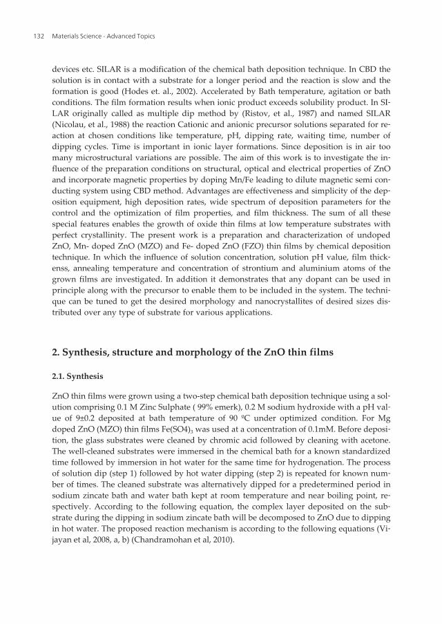
The crystallographic structure of the films has been studied by X-ray diffraction (XRD). Fig.1 shows the XRD spectrum of ZnO, MZO and FZO films deposited on the glass substrateunder optimized condition. It can be seen from the XRD data, that all samples are polycrys‐talline and exhibit the single-phase ZnO hexagonal wurtzite structure [JCPDS (36–1451)]. Allpeaks in recorded range were identified.
ZnO:Mn
(100
)(0
02)
(101
)
(102
)
(103
)(1
10)
(200
)
Figure 1. Typical XRD patterns of doped and undoped ZnO thin films
The XRD pattern clearly showed the polycrystalline nature of the ZnO, MZO and FZO films,whose c-axis was preferentially oriented normal to the glass substrate. In other words, thosegrains of undoped and doped films are mainly grown with c-axis vertical to the glass sub‐strate. Hence, the multiple-coating or the piling up of each film was considered not to dis‐turb the overall growth of the films with c-axis orientation. Therefore, the c-axis orientationmay be a common phenomenon in the ZnO film deposition by the chemical process usingorgano-zinc compounds. Such preferred basal orientation is typically observed also in metaldoped ZnO films (Vijayan et al, 2008, a, b) (Chandramohan et al, 2010). Moreover, from therecorded spectrums the minor diffraction peaks of (102) and (103) are approved of randomlyoriented of the ZnO film (Roy, at al., 2004). The crystallite size was estimated to be 80 nm forundoped film, 26 nm for MZO and 20 nm for FZO films from the Debye Scherrer formula.
Nanocrystalline Mn and Fe Doped ZnO Thin Films Prepared Using…http://dx.doi.org/10.5772/54327
133
2.3. Morphological studies
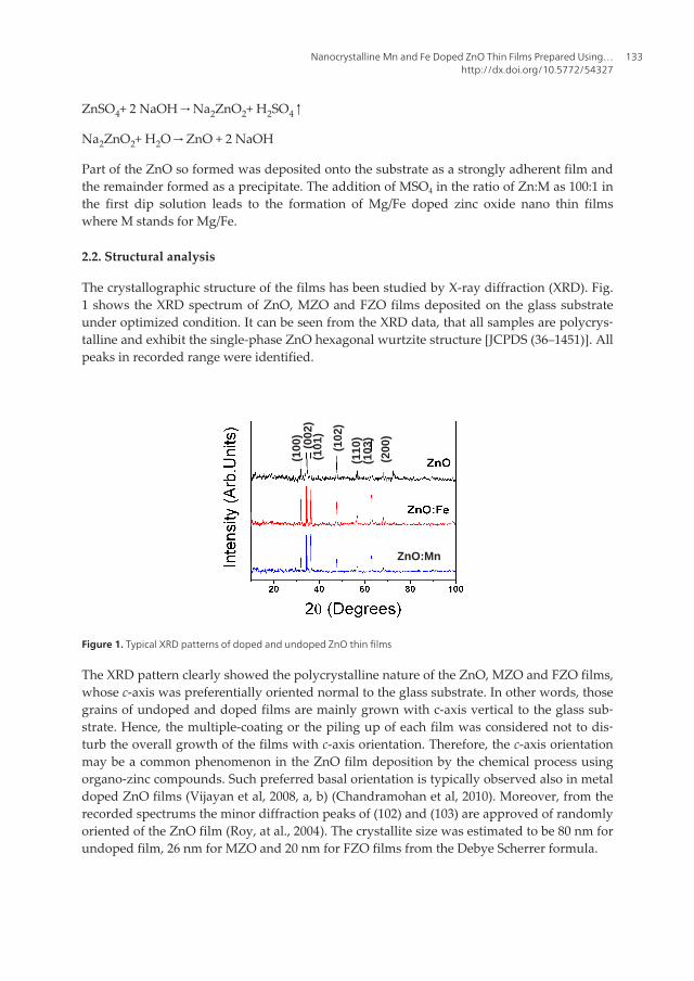
Figures 2(a, b, c) shows the scanning electron micrograph (SEM) of ZnO, MZO and FZOfilms deposited at room temperature. The SEM micrograph of MZO thin film show the uni‐form polycrystalline surface of the film with a hexagonal morphology consistent with XRDresult of P63mc crystal-structure with an average grain size of 300 nm. They are found to besingle-crystalline in nature. It can be seen that, films grown at room temperature by varyingMn and Fe concentration consist of slightly agglomerated particles with less voids in thesurface of the film with average grains 200 nm for undoped and 300 nm for doped ZnOfilms (Fig. 2(b)). This result confirmed that Mn and Fe doped into ZnO lattice and in goodagreement line with XRD result.
(a) (b)
(c)
Figure 2. (a,b,c,) Typical SEM micrographs obtained for (a) undoped ZnO thin films and (b) Mn (2%), (c) Fe (2%) dopedthin films prepared by SILAR
3. Optical properties of undoped and Fe doped ZnO thin films
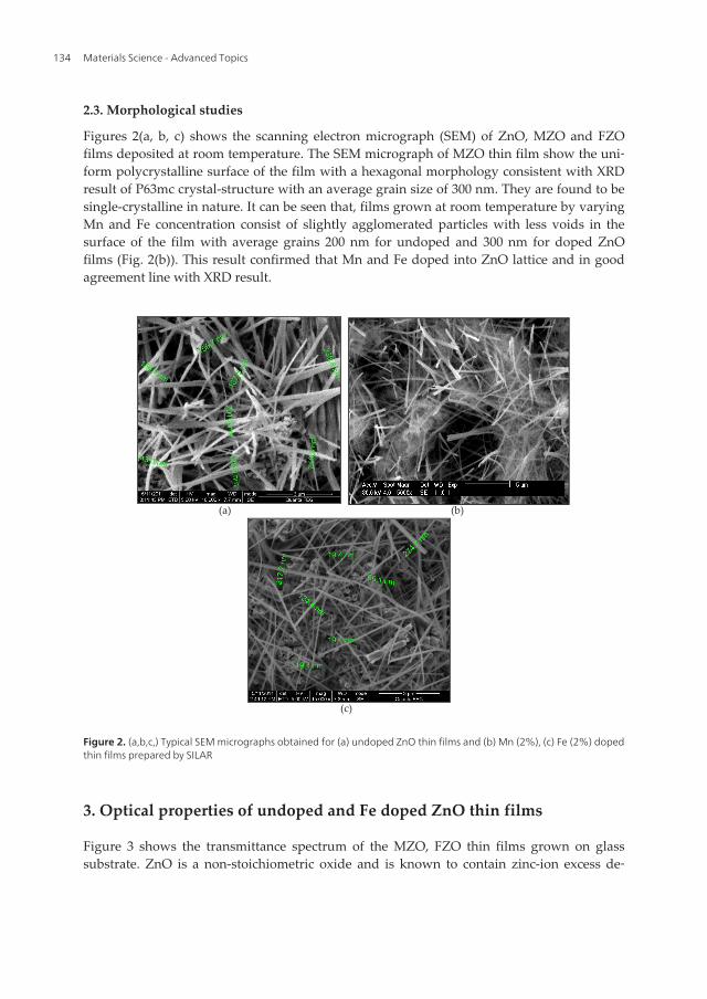
Figure 3 shows the transmittance spectrum of the MZO, FZO thin films grown on glasssubstrate. ZnO is a non-stoichiometric oxide and is known to contain zinc-ion excess de‐
Materials Science - Advanced Topics134
fects based on the presence of either zinc interstitial or oxygen vacancies. The films haveexcellent transmittance and very low absorption and reflectance. The optical band gap ofthe FZO and MZO thin films has decreased on Fe and Mn doping, respectively. Assumingdoping levels are well below Mott’s critical density, the change in optical band gap can beexplained in terms of Burstein–Moss band gap widening and band gap narrowing due tothe electron–electron and electron–impurity scattering. At high doping concentrations, fer‐mi level lifts into the conduction band. Due to filling of the conduction band, absorptiontransitions occurs between valance band and fermi level in the conduction band instead ofvalance band and bottom of the conduction band. This change in the absorption energylevels shifts the absorption edge to higher energies (blue shift) and leads to the energyband broadening. While on Mn and Fe doping into the ZnO matrix can explain the in‐crease in shift in the band gap value indicating that either it may due to any charged de‐fects or the charged defects formed had been neutralized by other defects. Hence, the blueshift in the band gap value by Mn and Fe doping suggest an increase in the n-type carrierconcentration, most of the Fe ions must be incorporated as interstitial donors into the struc‐ture rather than substitution of acceptors.
Figure 3. Optical transmittance of typical doped and undoped ZnO thin films
4. Magnetic properties of undoped and Mn, doped ZnO thin films
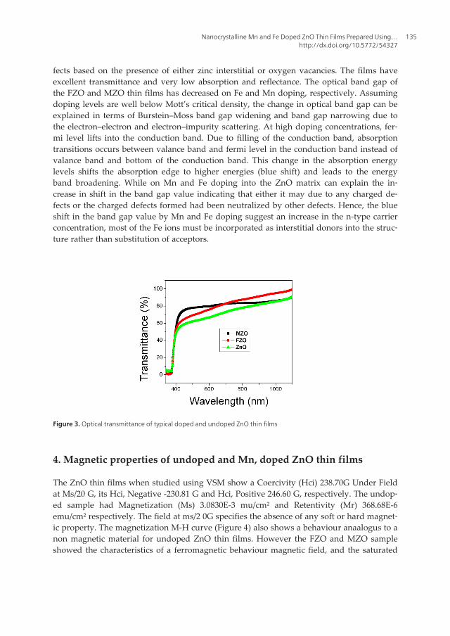
The ZnO thin films when studied using VSM show a Coercivity (Hci) 238.70G Under Fieldat Ms/20 G, its Hci, Negative -230.81 G and Hci, Positive 246.60 G, respectively. The undop‐ed sample had Magnetization (Ms) 3.0830E-3 mu/cm² and Retentivity (Mr) 368.68E-6emu/cm² respectively. The field at ms/2 0G specifies the absence of any soft or hard magnet‐ic property. The magnetization M-H curve (Figure 4) also shows a behaviour anaalogus to anon magnetic material for undoped ZnO thin films. However the FZO and MZO sampleshowed the characteristics of a ferromagnetic behaviour magnetic field, and the saturated
Nanocrystalline Mn and Fe Doped ZnO Thin Films Prepared Using…http://dx.doi.org/10.5772/54327
135
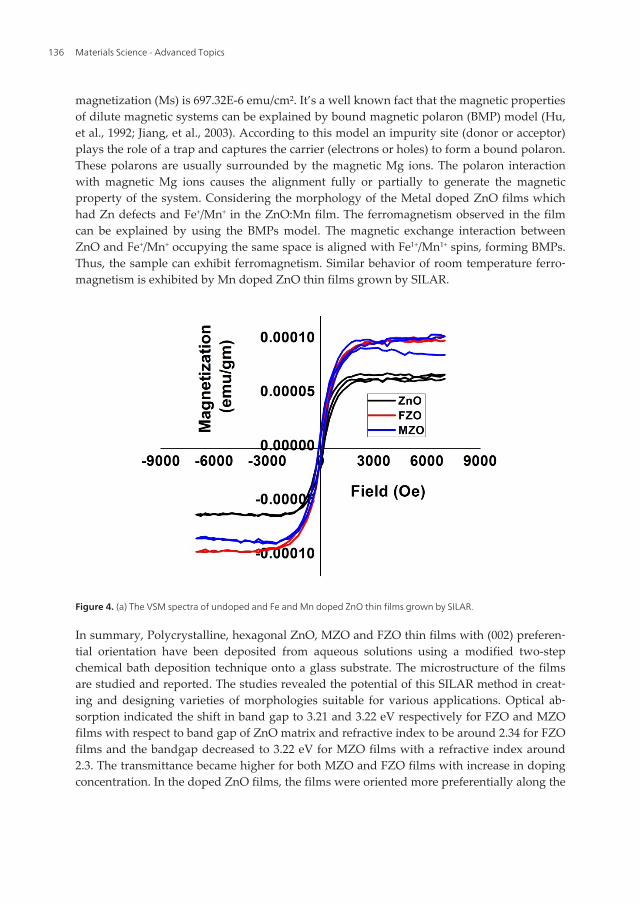
magnetization (Ms) is 697.32E-6 emu/cm². It’s a well known fact that the magnetic propertiesof dilute magnetic systems can be explained by bound magnetic polaron (BMP) model (Hu,et al., 1992; Jiang, et al., 2003). According to this model an impurity site (donor or acceptor)plays the role of a trap and captures the carrier (electrons or holes) to form a bound polaron.These polarons are usually surrounded by the magnetic Mg ions. The polaron interactionwith magnetic Mg ions causes the alignment fully or partially to generate the magneticproperty of the system. Considering the morphology of the Metal doped ZnO films whichhad Zn defects and Fe+/Mn+ in the ZnO:Mn film. The ferromagnetism observed in the filmcan be explained by using the BMPs model. The magnetic exchange interaction betweenZnO and Fe+/Mn+ occupying the same space is aligned with Fe1+/Mn1+ spins, forming BMPs.Thus, the sample can exhibit ferromagnetism. Similar behavior of room temperature ferro‐magnetism is exhibited by Mn doped ZnO thin films grown by SILAR.
Figure 4. (a) The VSM spectra of undoped and Fe and Mn doped ZnO thin films grown by SILAR.
In summary, Polycrystalline, hexagonal ZnO, MZO and FZO thin films with (002) preferen‐tial orientation have been deposited from aqueous solutions using a modified two-stepchemical bath deposition technique onto a glass substrate. The microstructure of the filmsare studied and reported. The studies revealed the potential of this SILAR method in creat‐ing and designing varieties of morphologies suitable for various applications. Optical ab‐sorption indicated the shift in band gap to 3.21 and 3.22 eV respectively for FZO and MZOfilms with respect to band gap of ZnO matrix and refractive index to be around 2.34 for FZOfilms and the bandgap decreased to 3.22 eV for MZO films with a refractive index around2.3. The transmittance became higher for both MZO and FZO films with increase in dopingconcentration. In the doped ZnO films, the films were oriented more preferentially along the
Materials Science - Advanced Topics136
(002) direction, the grain size of the films decreased, the transmittance also became higherand the electrical resistivities decreased. It is shown that doped ZnO thin films depositedwith a CBD technique can have high temperature ferromagnetic property and this transitionmay be explained by the BMP model. Extensive characterizations on the structure, micro‐structure optical and electrical properties have been made and the exotic choice available inthis simple method has paved way for the synthesis of many similar systems by our grouplike Fe, Mg and Mn doped ZnO thin films and other TCO systems like CdO, etc. Also theproperties of these thin film nanocrystallites can be tailored to suit variety of applicationslike, phosphors, display panels, thermal conduction and opto electronic devices. The techni‐que is easy for automation and anticorrosive coatings can be coated employing doped ZnOsystems on to various mechanical spares. The potential of this technique is yet to be exploit‐ed in full by the industrial community. The crystallite shape and size control is also feasiblein this excellent method.
Acknowledgements
Dr.R.C. Thanks UGC, New Delhi for supporting part of this work through a major researchproject. Also Dr. R.C thanks Dr. P. Parameshwaran PMD, MSG, IGCAR, Kalpakkam Indiaand C. Gopalakrishnan, Department of Nanotechnolgy, SRM University, Chennai extendingSEM facilities.
Author details
Rathinam Chandramohan1, Jagannathan Thirumalai2 andThirukonda Anandhamoorthy Vijayan2
1 Department of Physics,Sree Sevugan Annamalai College,Devakottai, Tamil Nadu, India
2 Department of Physics, B.S. Abdur Rahman University, Vandalur, Chennai, Tamil Nadu,India
References
[1] Chandramohan, R.; Thirumalai, J.; Vijayan, T. A.; ElhilVizhian, S.; Srikanth, S.; Val‐anarasu, S. & Swaminathan, V. (2010). Nanocrystalline Mg Doped ZnO Dilute Mag‐netic Semiconductor Prepared by Chemical Route. Adv. Sci. Lett. 3., 3., (September &2010) 319-322, ISSN: 1936-6612.
[2] Chapparro, M.; Maffiotte, C.; Gutierrez, M.T. & Herrero, J. (2003). Study of the spon‐taneous growth of ZnO thin films from aqueous solutions.Thin solid films., 431., 1.,(May & 2003) 373-377, ISSN: 0040-6090.
Nanocrystalline Mn and Fe Doped ZnO Thin Films Prepared Using…http://dx.doi.org/10.5772/54327
137
[3] Cheong, K.Y.; Muti, N.; Ramanan, S.R. (2002). Electrical and optical studies ofZnO:Ga thin films fabricated via the sol–gel technique. Thin Solid Films. 410., 1-2.,(May 2002), 142-146., ISSN: 0040-6090.
[4] Chou, T– L.; Ting, & J– M. (2005). Deposition and characterization of a novel integrat‐ed ZnO nanorods/thin film structure. Thin solid films. 494., 1-2., (January & 2006)291-295, ISSN: 0040-6090.
[5] Cracium, V.; Elders, J.; Gardeniers, J.G.E. & Boyd, L. W. (1994). Characteristics ofhigh quality ZnO thin films deposited by pulsed laser deposition. Appl. Phys. Lett.,65., 23., (October & 1994) 2963-2965., ISSN: 0003-6951.
[6] Das, S.; Chaudhuri, S. (2007). Mg2+ substitutions in ZnO–Al2O3 thin films and its ef‐fect on the optical absorption spectra of the nanocomposite. Appl. Surf. Sci., 253., 21.,8661-8668., ISSN: 0169-4332.
[7] Feng, Z–C.; Chen, C–F.; Kuo, C-T; Williams, K.; Shan, W. The 3rd Asian Conferenceon Chemical Vapor Deposition (3rd Asian-CVD), Taipei, Taiwan, November 12–14,2004. Thin solid films., 498., 1-2., (March & 2006) 1, ISSN: 0040-6090.
[8] Gorla, C.R.; Emanetoglu, N.W.; Liang, S.; Mayo, W.E.; Cu, Y.; Wraback, M. & Shen,H. (1999). Structural, optical, and surface acoustic wave properties of epitaxial ZnOfilms grown on (011-2) sapphire by metalorganic chemical vapor deposition. J. Appl.Phys., 85., 5., 2595-2602., ISSN 0021-8979.
[9] Hodes, G.; Chemical Solution Deposition of Semiconductor Films, Marcel DekkerInc., Oct. 2002.
[10] Hsu, H.H.; Paul Wang, H.; Chen, C.Y.; Jou C.J.G.; Wei, Y-L. (2007). Chemical struc‐ture of zinc in the Fe/ZnO thin films during sensing of ethanol, J. Elect. Spec. RelPhen., 156-158., (December & 2007), 344-346., ISSN: 0368-2048.
[11] Hu, J.; Gordon, R. G. (1992). Textured aluminum‐doped zinc oxide thin films fromatmospheric pressure chemical‐vapor deposition. J. Appl. Phys. 71., 2., (October &1991), 880-891, ISSN 0021-8979.
[12] Hu, J.; Gordon, R.G.; (1992). Textured aluminum‐doped zinc oxide thin films from at‐mospheric pressure chemical‐vapor deposition. J. Appl. Phys. 71., 2., (October 1991),880-890, ISSN 0021-8979.
[13] J. Cryst. Growth 237–239., Part 1., ( December & 2001), 538-543., ISSN: 0022-0248.
[14] J. Cryst. Growth. 92., 1-2., (October & 1988) 128-142., ISSN: 0022-0248.
[15] J. S. Wellings, A. P. Samantilleke, P. Warren, S. N. Heavens and I. M. Dharmadasa.(2008). Comparison of electrodeposited and sputtered intrinsic and aluminium-dop‐ed zinc oxide thin films. Semicond. Sci. Technol. 23., 12., (August & 2008)125003-125009, ISSN 0268-1242.
Materials Science - Advanced Topics138
[16] Jiang, X.; Wong, F.L.; Fung, M.K.; Lee, S.T. (2003). Aluminum-doped zinc oxide filmsas transparent conductive electrode for organic light-emitting devices. Appl. Phys.Lett. 83., (July & 2003), 1875-1877, ISSN: 0003-6951.
[17] Jiang, X.; Wong, F.L.; Fung, M.K.; Lee, S.T.; (2003). Aluminum-doped zinc oxide filmsas transparent conductive electrode for organic light-emitting devices. Appl. Phys.Lett. 83., 9., (July & 2003), 1875-1877., ISSN 0003-6951.
[18] Kato, H.; Sano, M.; Miyamoto, K.; Yao, T. (2002). Growth and characterization of Ga-doped ZnO layers on a-plane sapphire substrates grown by molecular beam epitaxy.
[19] Kotlyarchuk, B.; Sarchuk, V. & Oszwaldowski, M. (2005). Preparation of undopedand indium doped ZnO thin films by pulsed laser deposition method. Cryst. Res.Technol., 40., 12., (December & 2005) 1118- 1123, ISSN: 0232-1300.
[20] Liu, C.; Yun, F.; & Morkoç, H, (2005). Ferromagnetism of ZnO and GaN: A Review J.Mater. Sci: Mat in Electronics. 16., 9., 555-597, ISSN: 0957-4522.
[21] Lokhande, B.J. & Uplane, M.D. (2000). Structural, optical and electrical studies onspray deposited highly oriented ZnO films. Appl. Surf. Sci., 167., 3-4., (October &2000) 243-246, ISSN: 0169-4332.
[22] Mitra, P.; Chatterjee, A.P. & Maiti, H.S. (1998). Chemical deposition of ZnO films forgas sensors. J. Mater. Sci: Mat in Electronics., 9., 6., (December & 1998) 441-445, ISSN:0957-4522.
[23] Natsume, Y. & Sakata, H. (2000). Zinc oxide films prepared by sol-gel spin-coating.Thin solid films., 372., 1-2., (September & 2000) 30-36, ISSN: 0040-6090.
[24] Nicolau, Y.F.; Menard, J.C.,; (1988). Solution growth of ZnS, CdS and Zn1-xCdxS thinfilms by the successive ionic-layer adsorption and reaction process growth mecha‐nism.
[25] Nielsen, A.; Brandlmaier, A.; Althammer, M.; Kaiser, W.; Opel, M.; Simon, J.; Mader,W.; Goennenwein, S.T.B.; Gross, R. (2008). All Oxide Ferromagnet/SemiconductorEpitaxial Heterostructures. Appl. Phys. Lett. 93., 16., (October & 2008) 162510-3.,ISSN: 0003-6951.
[26] Pawar, B.N.; Jadkar, S.R.; Takwale, M.G. (2005). Deposition and characterization oftransparent and conductive sprayed ZnO:B thin films. J. Phys. Chem. Solids. 66., 10.,(November & 2005) 1779-1782., ISSN: 0022-3697.
[27] Peiro, A. M.; Ayllon, J. A.; Pearl, J.; Domenech, X. & Domingo C. (2005). Microwaveactivated chemical bath deposition (MW-CBD) of zinc oxide: Influence of bath com‐position and substrate characteristics. J. Crystal. Growth., 285., 1-2., (November&2005) 6-16, ISSN: 0022-0248.
[28] Piticescu, R. R. Piticescu, R. M. & Monty, C. J. (2006). Synthesis of Al-doped ZnOnanomaterials with controlled luminescence. J. Europ. Cer. Soc. 26., 14., (March &2006) 2979-2983, ISSN: 0955-2219.
Nanocrystalline Mn and Fe Doped ZnO Thin Films Prepared Using…http://dx.doi.org/10.5772/54327
139
[29] Ramamoorthy, K.; Arivanandhan, M.; Sankaranarayanan, K. & Sanjeeviraja, C.(2004). Mater. Chem. Phys., 85., 2-3., (June & 2004) 257-262, ISSN: 0254-0584.
[30] Ristov, M.; Sinadinovski, G.; Grozdanov, I.; Mitreski, M. (1987).Chemical depositionof ZnO films. Thin Solid Films. 149., 1., (May & 1987), 65-71., ISSN: 0040-6090.
[31] Roy, V. A. L.; Djurisic, A. B.; Liu, H.; Zhang, X. X.; Leung, Y. H.; Xie, M. H.; Gao, J.;Lui, H. F.; Surya, C. (2004). Magnetic properties of Mn doped ZnO tetrapod struc‐tures. Appl. Phys. Lett. 84, 5., (2004), 756-759., ISSN: 0003-6951.
[32] Ryu, Y. R.; Zhu, S.; Budai, J. D.; Chandrasekhar, H. R.; Miceli, P. F.; White, H.W.(2000). Optical and structural properties of ZnO films deposited on GaAs by pulsedlaser deposition. J. Appl. Phys. 88., 1., 201-204, ISSN: 0021-4922.
[33] Sadrnezhaad, S.K. & Vaezi, M.R. (2006). The effect of addition of Tiron as a surfactanton the microstructure of chemically deposited zinc oxide. Mat. Sci. Engg: B., 128.,1-3., (March & 2006) 53-57, ISSN: 0921-5107.
[34] Saeed, T. & Brien, P. O’. (1995). Deposition and characterisation of ZnO thin filmsgrown by chemical bath deposition. Thin solid films., 271., 1-2., (December & 1995)35-38, ISSN: 0040-6090.
[35] Srinivasan, G. & Kumar, J. (2006). Optical and structural characterisation of zinc ox‐ide thin films prepared by sol-gel process. Cryst. Res. Technol. 41., 9., (September &2006) 893- 896, ISSN: 0232-1300.
[36] Tang, Z.K.; Wang, G.K. L.; Yu, P.; Kawaraki, M.; Ohtomo, A.; Koinuma, H. & Sega‐wa, Y. (1998). Appl. Phys. Lett. 72., 3270, ISSN: 0003-6951.
[37] Vijayan, T. A.; Chandramohan, R.; Valanarasu, S.; Thirumalai, J.; Venkateswaran, S.;Mahalingam, T. & Srikumar, S.R. (2008). Optimization of growth conditions of ZnOnano thin films by chemical double dip technique. Sci. Tech. Adv. Mater., 9., (April &2008) 035007, ISSN: 1468-6996.
[38] Vijayan, T. A.; Chandramohan, R.; Valanarasu, S.; Thirumalai, J.; Subramanian, S. P.(2008). Comparative investigation on nanocrystal structure, optical, and electricalproperties of ZnO and Sr-doped ZnO thin films using chemical bath depositionmethod. J. Mater. Sci., 43., 6., (March & 2008) 1776–1782, ISSN: 0022-2461.
[39] Vijayan, T. A.; Chandramohan, R.; Valanarasu, S.; Thirumalai, J.; Subramanian, S. P.(2008). Comparative investigation on nanocrystal structure, optical, and electricalproperties of ZnO and Sr-doped ZnO thin films using chemical bath depositionmethod. J. Mater. Sci., 43., 6., (March & 2008) 1776–1782, ISSN: 0022-2461.
[40] Wang, L.; Giles, N. C. (2003). Temperature dependence of the free-exciton transitionenergy in zinc oxide by photoluminescence excitation spectroscopy. J. Appl. Phys.94., 2., 973-978., ISSN: 0021-4922.
Materials Science - Advanced Topics140

[41] Wei, X. X.; C Song, K W Geng, F Zeng, B He and F Pan. (2006). Local Fe structure and
ferromagnetism in Fe-doped ZnO films. J. Phys.: Condens. Matter. 18., 31., (July &
2006) 7471-7479., ISSN 0953-8984.
[42] Yang, Y.; Tay, B.K.; Sun, X.W.; Han, Z.J.; Shen, Z.X.; Lincoln, C.; & Smith, T, (2008).
Nanoelectronics Conference, INEC 2008 2 nd IEEE International, Nanyang Technical
University, Singapore 24-27 March 2008.
[43] Yang, Z. X.; Zhong, W.; Au, C. T.; Du, X.; Song, H. A.; Qi, X. S.; Ye, X. J.; Xu M. H.;
Du, Y. W. (2009). Novel Photoluminescence Properties of Magnetic Fe/ZnO Compo‐
sites: Self-Assembled ZnO Nanospikes on Fe Nanoparticles Fabricated by Hydro‐
thermal Method. J. Phys. Chem. C., 113., 51., (November & 2009) 21269 – 21273.,
ISSN: 1932-7447.
[44] Zhou, H–M.; Yi, D–Q.; Yu, Z–M.; Rang, L.; Xiao, Li, J. (2007). Preparation of alumi‐
num doped zinc oxide films and the study of their microstructure, electrical and opti‐
cal properties. Thin solid films., 515., 17., (June 2007) 6909-6914, ISSN: 0040-6090.
Nanocrystalline Mn and Fe Doped ZnO Thin Films Prepared Using…http://dx.doi.org/10.5772/54327
141