Embed Size (px)
Citation preview
University of South FloridaScholar Commons
Graduate Theses and Dissertations Graduate School
2011
Electronic Structure Characterization ofNanocrystalline Surfaces and Interfaces withPhotoemission SpectroscopySebastian GutmannUniversity of South Florida, [email protected]
Follow this and additional works at: http://scholarcommons.usf.edu/etd
Part of the American Studies Commons, and the Physical Chemistry Commons
This Dissertation is brought to you for free and open access by the Graduate School at Scholar Commons. It has been accepted for inclusion inGraduate Theses and Dissertations by an authorized administrator of Scholar Commons. For more information, please [email protected].
Scholar Commons CitationGutmann, Sebastian, "Electronic Structure Characterization of Nanocrystalline Surfaces and Interfaces with PhotoemissionSpectroscopy" (2011). Graduate Theses and Dissertations.http://scholarcommons.usf.edu/etd/3137
Electronic Structure Characterization of Nanocrystalline Surfaces and Interfaces
with Photoemission Spectroscopy
by
Sebastian Gutmann
A dissertation submitted in partial fulfillment
of the requirements of the degree of
Doctor of Philosophy
Department of Chemistry
College of Arts and Sciences
University of South Florida
Major Professor: Rudy Schlaf, Ph.D.
Matthias Batzill, Ph.D.
Brian Space, Ph.D.
Michael Zaworotko, Ph.D.
Date of Approval:
October 14, 2011
Keywords: electrospray, work function, titanium dioxide,
dye-sensitized solar cell, zinc oxide, cadmium selenide
Copyright © 2011, Sebastian Gutmann

DEDICATION
This dissertation is dedicated to my dear wife Youjin. Thank you for accepting the
challenging times and tolerating the effort and energy it took to get where we are now.
You have given me two wonderful children and made me a very proud man. I truly
appreciate your commitment to Younis and Youna. I love you.

ACKNOWLEDGEMENTS
First and foremost, I would like to express my sincere gratitude to
Professor Dr. Schlaf, who has supervised the work required to complete this dissertation.
I am very thankful for his guidance and support.
Furthermore, I am thankful to the members of my supervisory committee for
providing advice on how to improve my work.
I would like to thank Dr. Beerbom and all members of the Surface Science
Laboratory at the University of South Florida.
And of course, I am very grateful to my parents Monika and Klaus Gutmann, my
brother Robert, and my parents-in-law Okhyu Shin and Jeongkuk Kim, who have always
encouraged and cared about me and made the fulfillment of my dreams possible.

i
TABLE OF CONTENTS
LIST OF TABLES ............................................................................................................. iii
LIST OF FIGURES ........................................................................................................... iv
LIST OF ABBREVIATIONS ............................................................................................. x
ABSTRACT ...................................................................................................................... xii
CHAPTER 1: INTRODUCTION AND FUNDAMENTALS ............................................ 1 1.1 Motivation and outline of this dissertation ...................................................... 1
1.2 Semiconductor nanoparticle properties ........................................................... 4 1.3 Nanoparticle based photovoltaics .................................................................... 9 1.4 Semiconductor surface and interface electronic structures ........................... 14
CHAPTER 2: EXPERIMENTAL METHODOLOGY .................................................... 19 2.1 Electrospray technique .................................................................................. 19
2.1.1 Electrospray for thin film deposition ............................................ 19 2.1.2 Physical principle .......................................................................... 21
2.2 Photoemission spectroscopy .......................................................................... 22
2.2.1 Physical principle .......................................................................... 23
2.2.2 Instrumentation.............................................................................. 27 2.2.3 X-ray photoemission spectroscopy (XPS) .................................... 29 2.2.4 Ultraviolet photoemission spectroscopy (UPS) ............................ 33
2.2.5 Low intensity x-ray photoemission spectroscopy (LIXPS) .......... 36 2.3 Optical absorption spectroscopy ................................................................... 38
2.4 Experimental setup ........................................................................................ 42 2.4.1 Equipment ..................................................................................... 42
2.4.2 Sample preparation ........................................................................ 45 2.4.3 Measurement sequence and data analysis ..................................... 46
CHAPTER 3: ELECTRONIC STRUCTURE OF NANOCRYSTALLINE
TITANIUM DIOXIDE AND ITO/TiO2 INTERFACES ............................................ 48
3.1 Work function measurements on nanocrystalline TiO2 surfaces .................. 48 3.2 Electronic structure of ITO/nanocrystalline TiO2 interfaces ......................... 53
CHAPTER 4: INVESTIGATION OF WORK FUNCTION CHANGES ON
NANOCRYSTALLINE ZINC OXIDE SURFACES ................................................. 59 4.1 Introduction ................................................................................................... 59 4.2 Experimental ................................................................................................. 61 4.3 Results ........................................................................................................... 61 4.4 Discussion ..................................................................................................... 69
ii
CHAPTER 5: ELECTRONIC STRUCTURE OF FUNCTIONALIZD
CADMIUM SELENIDE NANOPARTICLES ........................................................... 75 5.1 Introduction ................................................................................................... 75 5.2 Experimental ................................................................................................. 80
5.3 Results ........................................................................................................... 82 5.4 Discussion ..................................................................................................... 95
CONLUSIONS ............................................................................................................... 103
REFERENCES ............................................................................................................... 106
APPENDIX A: COPYRIGHT APPROVAL .................................................................. 117
APPENDIX B: PUBLICATION 1: EFFECT OF ULTRAVIOLET AND X-RAY
RADIATION ON THE WORK FUNCTION OF TiO2 SURFACES ...................... 124
APPENDIX C: PUBLICATION 2: ELECTRONIC STRUCTURE OF INDIUM
TIN OXIDE / NANOCRYSTALLINE TiO2 INTERFACES AS USED IN
DYE-SENSITIZED SOLAR CELL DEVICES ....................................................... 133
ABOUT THE AUTHOR…………………………………………………….…...End Page

iii
LIST OF TABLES
Table 1: Ionization cross section at 1254 eV for electrons from selected orbitals,
[56] .............................................................................................................................. 24
iv
LIST OF FIGURES
Figure 1: Electronic energy level evolution from a single atom to bulk
semiconductor. Band gap energies increase from bulk to nanocrystal, while
energy bands become discrete at the edges. .................................................................. 5
Figure 2: Surface to volume ratio vs. particle diameter. At a diameter below
10 nm the surface to volume ratio increases rapidly. .................................................... 8
Figure 3: SEM image of a nanoporous TiO2 film as used in dye-sensitized solar
cells ............................................................................................................................... 9
Figure 4: Operation principle of a dye-sensitized solar cell. The absorption of a
photon generates an excited dye molecule (dye*). The electron injection
occurs into the conduction band of the nanocrystalline TiO2 from where
electrons diffuse to the ITO front contact. The Pt back contact is being
oxidized and the iodide/triiodide mediator forms a regenerative cycle that
donates electrons to the dye. ....................................................................................... 11
Figure 5: Energy level diagram of an excitonic hetero-junction solar cell. The
optical band gap energy is less than the energy required to produce a free
electron and hole (electrical band gap). But the exciton created by light
absorption dissociates into separate charges at the interface, because the band
offset between the two materials provides an exothermic pathway for
dissociation. ................................................................................................................ 12
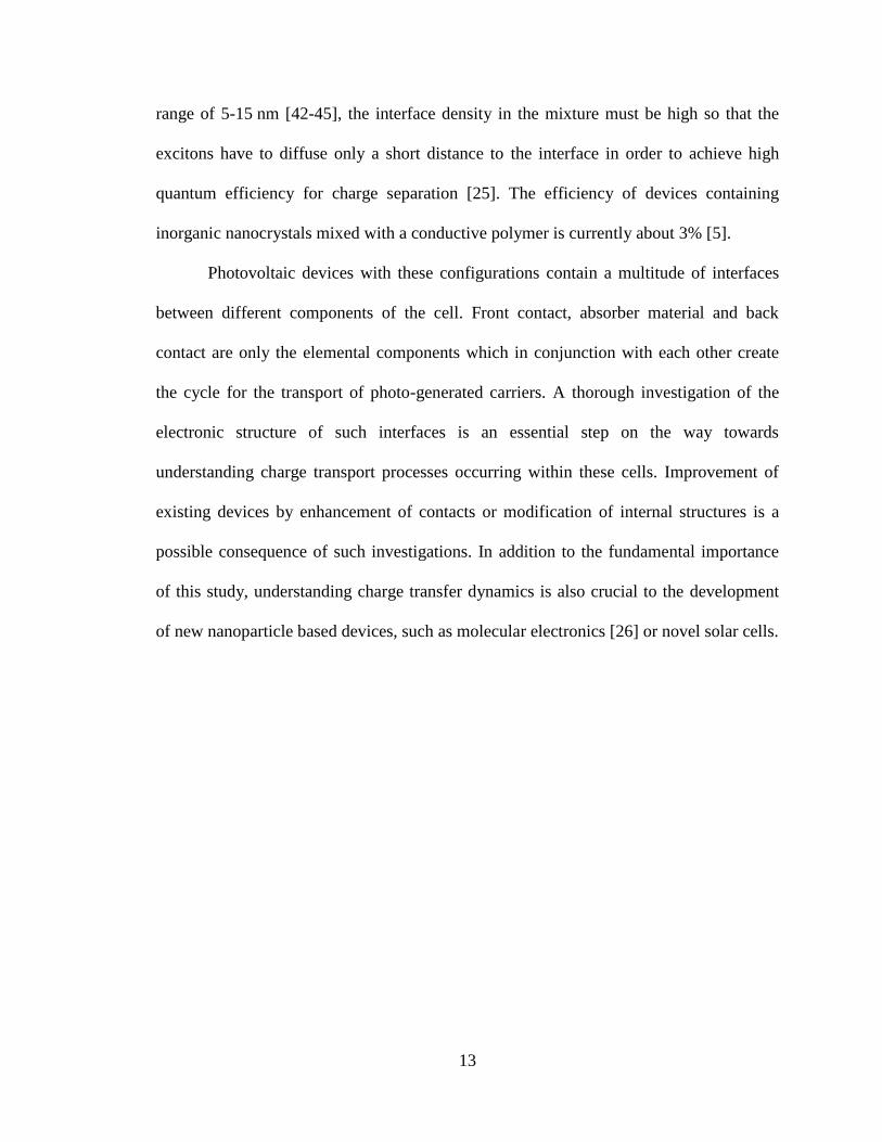
Figure 6: Semiconductor band structure, (a) flat band situation, (b) surface band
bending, (c) presence of a positive surface dipole ...................................................... 14
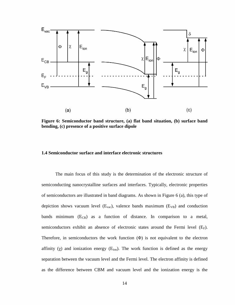
Figure 7: Formation of a semiconductor hetero-interface. (a) shows the two
semiconductors before contact. After thermodynamic equilibrium is reached
(b) the Fermi levels are aligned and a surface dipole δ is formed. ............................. 16
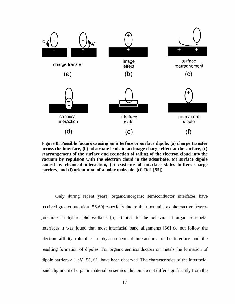
Figure 8: Possible factors causing an interface or surface dipole. (a) charge
transfer across the interface, (b) adsorbate leads to an image charge effect at
the surface, (c) rearrangement of the surface and reduction of tailing of the
electron cloud into the vacuum by repulsion with the electron cloud in the
adsorbate, (d) surface dipole caused by chemical interaction, (e) existence of
interface states buffers charge carriers, and (f) orientation of a polar molecule.
(cf. Ref. [55]) .............................................................................................................. 17
v
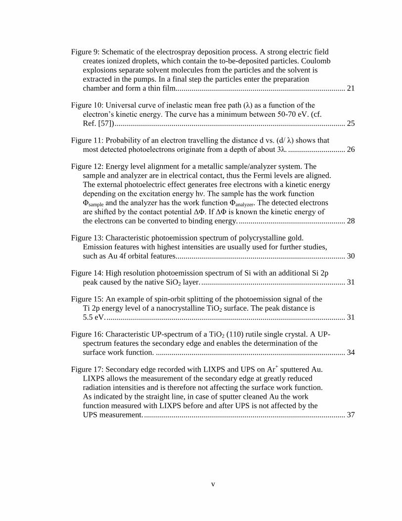
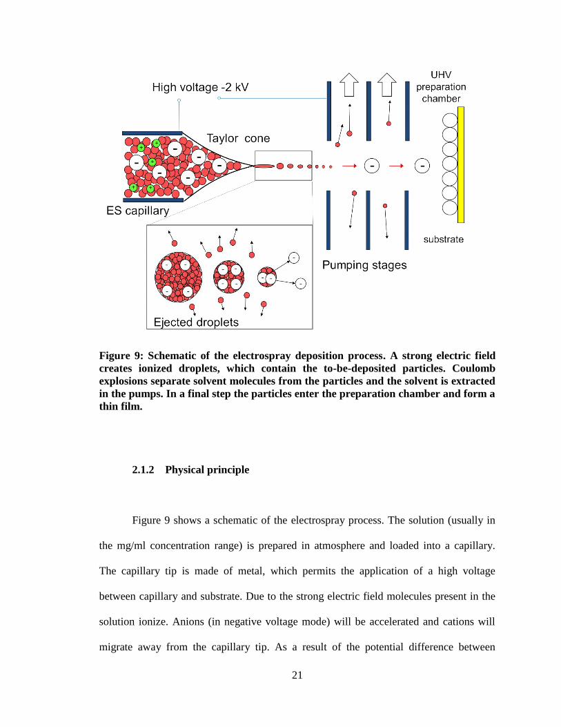
Figure 9: Schematic of the electrospray deposition process. A strong electric field
creates ionized droplets, which contain the to-be-deposited particles. Coulomb
explosions separate solvent molecules from the particles and the solvent is
extracted in the pumps. In a final step the particles enter the preparation
chamber and form a thin film...................................................................................... 21
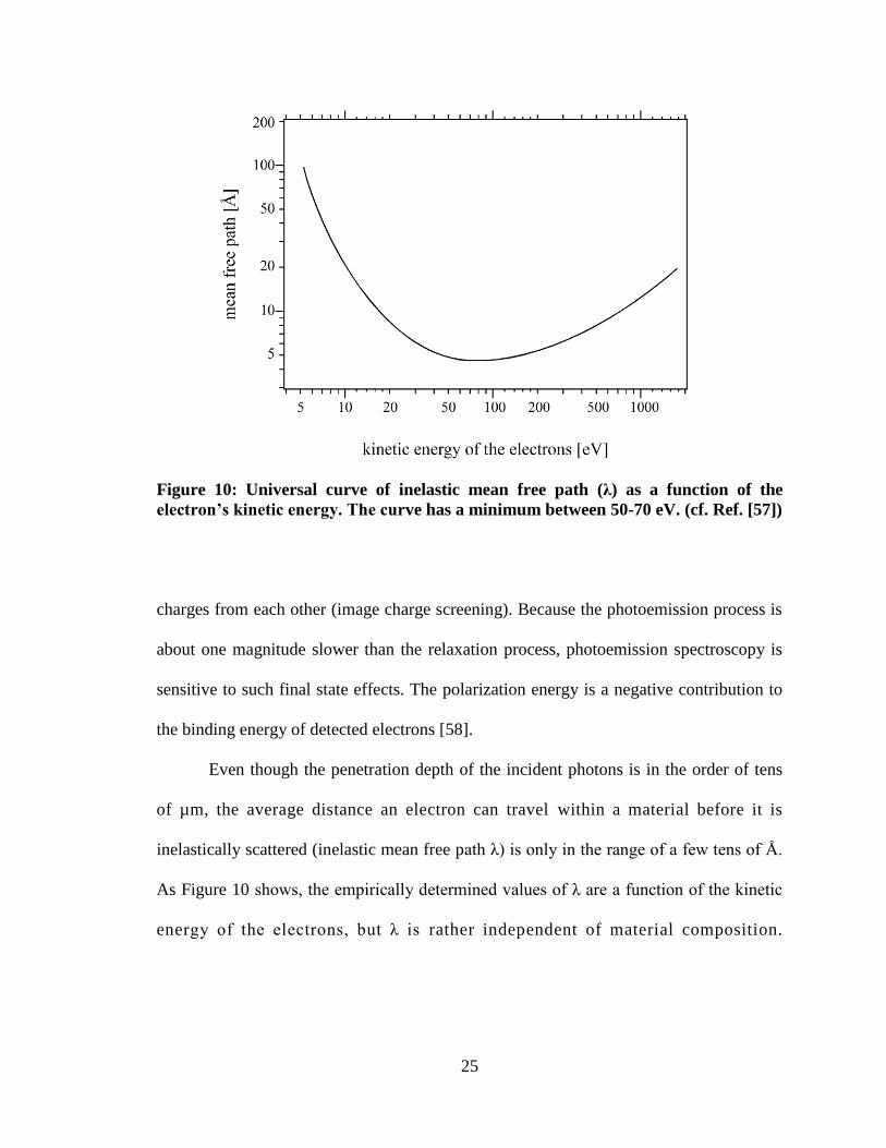
Figure 10: Universal curve of inelastic mean free path (λ) as a function of the
electron‟s kinetic energy. The curve has a minimum between 50-70 eV. (cf.
Ref. [57]) ..................................................................................................................... 25
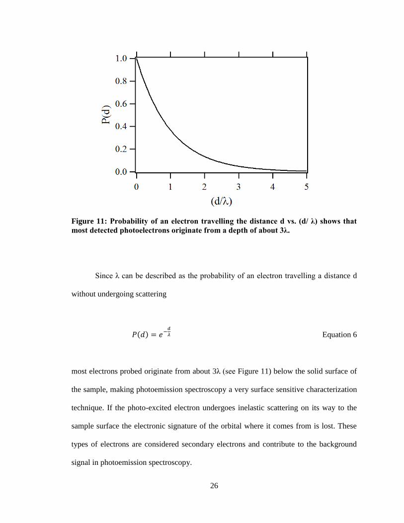
Figure 11: Probability of an electron travelling the distance d vs. (d/ λ) shows that
most detected photoelectrons originate from a depth of about 3λ. ............................. 26
Figure 12: Energy level alignment for a metallic sample/analyzer system. The
sample and analyzer are in electrical contact, thus the Fermi levels are aligned.
The external photoelectric effect generates free electrons with a kinetic energy
depending on the excitation energy hν. The sample has the work function
Φsample and the analyzer has the work function Φanalyzer. The detected electrons
are shifted by the contact potential ΔΦ. If ΔΦ is known the kinetic energy of
the electrons can be converted to binding energy. ...................................................... 28
Figure 13: Characteristic photoemission spectrum of polycrystalline gold.
Emission features with highest intensities are usually used for further studies,
such as Au 4f orbital features...................................................................................... 30
Figure 14: High resolution photoemission spectrum of Si with an additional Si 2p
peak caused by the native SiO2 layer. ......................................................................... 31
Figure 15: An example of spin-orbit splitting of the photoemission signal of the
Ti 2p energy level of a nanocrystalline TiO2 surface. The peak distance is
5.5 eV. ......................................................................................................................... 31
Figure 16: Characteristic UP-spectrum of a TiO2 (110) rutile single crystal. A UP-
spectrum features the secondary edge and enables the determination of the
surface work function. ................................................................................................ 34
Figure 17: Secondary edge recorded with LIXPS and UPS on Ar+ sputtered Au.
LIXPS allows the measurement of the secondary edge at greatly reduced
radiation intensities and is therefore not affecting the surface work function.
As indicated by the straight line, in case of sputter cleaned Au the work
function measured with LIXPS before and after UPS is not affected by the
UPS measurement. ...................................................................................................... 37
vi
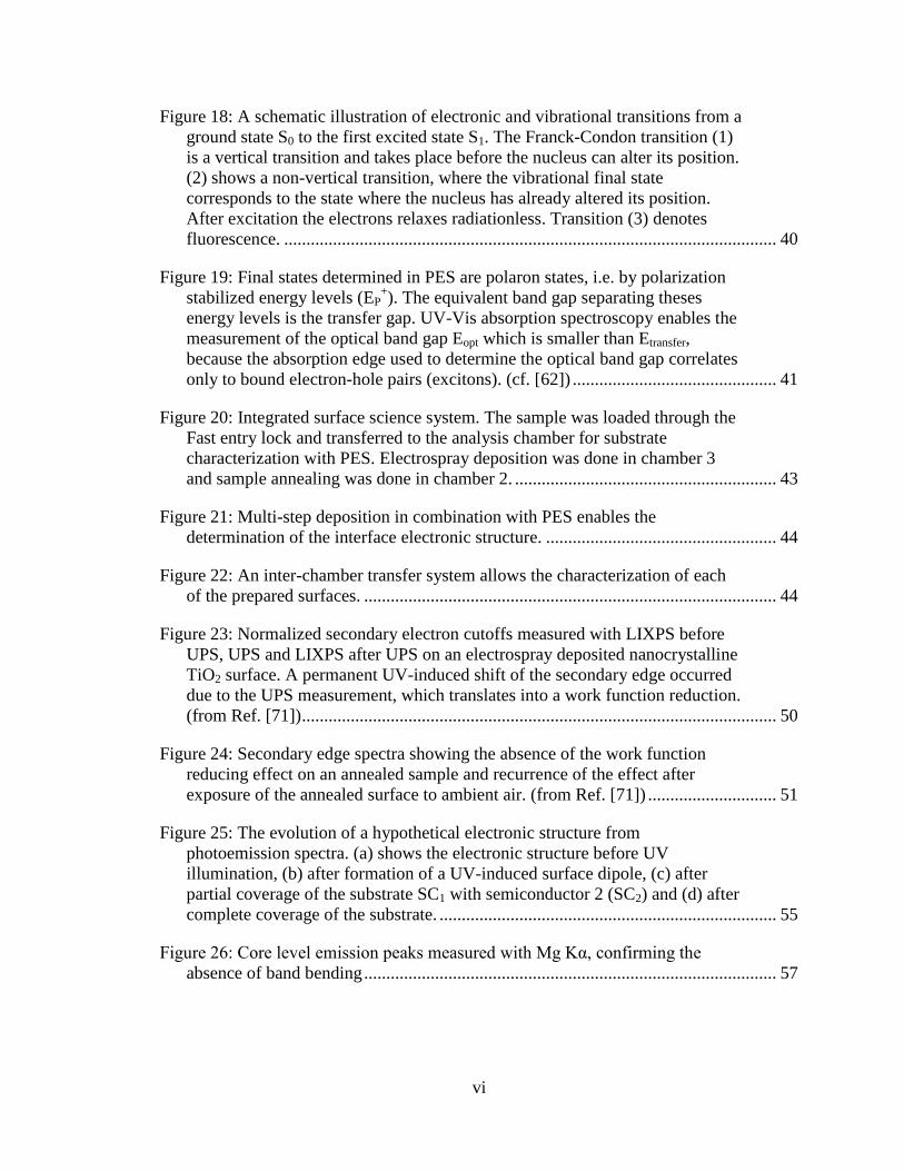
Figure 18: A schematic illustration of electronic and vibrational transitions from a
ground state S0 to the first excited state S1. The Franck-Condon transition (1)
is a vertical transition and takes place before the nucleus can alter its position.
(2) shows a non-vertical transition, where the vibrational final state
corresponds to the state where the nucleus has already altered its position.
After excitation the electrons relaxes radiationless. Transition (3) denotes
fluorescence. ............................................................................................................... 40
Figure 19: Final states determined in PES are polaron states, i.e. by polarization
stabilized energy levels (EP+). The equivalent band gap separating theses
energy levels is the transfer gap. UV-Vis absorption spectroscopy enables the
measurement of the optical band gap Eopt which is smaller than Etransfer,
because the absorption edge used to determine the optical band gap correlates
only to bound electron-hole pairs (excitons). (cf. [62]) .............................................. 41
Figure 20: Integrated surface science system. The sample was loaded through the
Fast entry lock and transferred to the analysis chamber for substrate
characterization with PES. Electrospray deposition was done in chamber 3
and sample annealing was done in chamber 2. ........................................................... 43
Figure 21: Multi-step deposition in combination with PES enables the
determination of the interface electronic structure. .................................................... 44
Figure 22: An inter-chamber transfer system allows the characterization of each
of the prepared surfaces. ............................................................................................. 44
Figure 23: Normalized secondary electron cutoffs measured with LIXPS before
UPS, UPS and LIXPS after UPS on an electrospray deposited nanocrystalline
TiO2 surface. A permanent UV-induced shift of the secondary edge occurred
due to the UPS measurement, which translates into a work function reduction.
(from Ref. [71]) ........................................................................................................... 50
Figure 24: Secondary edge spectra showing the absence of the work function
reducing effect on an annealed sample and recurrence of the effect after
exposure of the annealed surface to ambient air. (from Ref. [71]) ............................. 51
Figure 25: The evolution of a hypothetical electronic structure from
photoemission spectra. (a) shows the electronic structure before UV
illumination, (b) after formation of a UV-induced surface dipole, (c) after
partial coverage of the substrate SC1 with semiconductor 2 (SC2) and (d) after
complete coverage of the substrate. ............................................................................ 55
Figure 26: Core level emission peaks measured with Mg Kα, confirming the
absence of band bending ............................................................................................. 57
vii
Figure 27: Normalized secondary electron cutoff of low intensity XP and UP-
spectra measured on an electrospray deposited nanocrystalline ZnO thin film.
The bottom spectrum was measured using low-intensity x-ray photoemission
spectroscopy (LIXPS), which enables the determination of the work function
prior to UV exposure. The center spectrum was measured using UPS and
indicates a shift of the secondary edge to lower kinetic energy. The top
spectrum was recorded with a post-UPS LIXPS measurement confirming the
permanence of the UV-induced work function reduction. .......................................... 62
Figure 28: The left panel shows the result of single scan LIXPS measurement
performed during a period of 64 min after the conclusion of the LIXPS-UPS-
LIXPS sequence shown in Figure 27 to detect potential sample charging. The
right panel plots the work function values extracted from these scans vs. time,
as well as the initial three values from the spectra shown in Figure 27. The
graph shows that the work function partially recovers to a higher value after
conclusion of the UPS measurement. This indicates that sample charging
contributed 0.15 eV to the observed shift of the secondary edge during the
UPS measurement. This allowed the conclusion that the permanent part of the
work function reduction amounts to 0.35 eV. ............................................................. 63
Figure 29: The bottom graph shows the result of a LIXPS-UPS-LIXPS sequence
measured on nanocrystalline ZnO sample where ambient contamination, as
well as the solubility enhancing organic ligands were removed through an
annealing step at 400°C. It is obvious that this sample did not show the work
function reduction artifact during the UPS measurement. This allowed the
conclusion that water needs to be present for the effect to occur. The top graph
shows the situation on the same sample after re-exposing it to the ambient,
effectively re-coating it with an ambient water layer. The LIXPS-UPS-LIXPS
sequence shows that the artifact re-appeared, supporting the conclusions that
water is necessary and that the surfactant molecules do not play a major role. ......... 65
Figure 30: XPS core level spectra measured on the electrospray deposited ZnO
surface (a), after annealing (b) and after exposure to ambient atmosphere (c).
The bottom spectrum shows additional peaks that can be associated with the
presence of an organic ligand shell on the ZnO nanocrystals. After annealing
the adsorbates are removed, and the spectra indicate a clean ZnO surface.
After re-exposure to the ambient the Zn 2p3/2 and O 1s emission lines shifted
by ~0.2 eV to higher binding energy indicating the development of a surface
potential (“band bending”). ......................................................................................... 66
viii
Figure 31: Valence band spectra measured with UPS on the electrospray
deposited nanocrystalline ZnO surface (a), the annealed surface (b) and the
ambient exposed surface (c). Due to the presence of a surfactant on the
nanocrystals, ZnO related valence band features cannot be discerned on the
“as deposited” spectrum. After annealing the typical valence bands features of
ZnO appeared. A valence bands maximum of 3.0 eV was determined on the
annealed sample (b). After re-exposure to the ambient the valence bands
maximum shifts to 3.3 eV matching the shift on the core levels shown in
Figure 30. .................................................................................................................... 68
Figure 32: Electronic structure of the annealed sample (left) and the same sample
after exposure to the ambient and UPS measurement (right). The annealed
sample shows a work function of 4.1 eV, and a Fermi level about 0.2 eV
below the conduction bands minimum (CBM) indicating n-doping. Exposure
to the ambient and subsequent UPS characterization pushes the Fermi level
onto the CBM, while reducing the work function to 4.0 eV due to the
formation of a photochemically formed surface dipole based on OH-groups
attached to oxygen vacancies on the ZnO surface. ..................................................... 74
Figure 33: Schematic of a conductive polymer/CdSe nanocrystal composite. (a)
The coating of the CdSe nanocrystal with TOPO molecules constitutes a
barrier for charge separation. (b) an increase in charge separation efficiency
can be expected upon functionalization of the hybrid nanocrystals and direct
linkage to the conductive polymer phase. ................................................................... 76
Figure 34: Measurement approach to determine inner-molecular electronic
structures in CdSe/ligand hybrid nanoparticles. The isolated nanoparticle and
organic component are characterized and core-level to VBM (HOMO)
binding energy differences are obtained. In combination with the recorded
core-levels in the hybrid material it is then possible to determine molecule
internal charge injection barriers. ............................................................................... 79
Figure 35: Chemical structure of the arylselenophosphate (ArSeP) ligand ...................... 81
Figure 36: TEM image of the functionalized CdSe nanocrystals prepared by
addition of arylselenophosphate ligand to the reaction mixture after 9 min.
The nanocrystals have a diameter of ~8 nm. .............................................................. 82
Figure 37: Secondary electron cutoff measured on CdSe nanoparticle thin film
with LIXPS reveals a marginal work function change of 0.1 eV due to the
UPS measurement. The analysis of the valence band structure reveals a VBM
of 2.3 eV...................................................................................................................... 83
Figure 38: Cd 3d5/2 core-level emission features recorded on (pyridine)-capped
CdSe nanoparticles (bottom) and on the functionalized hybrid CdSe
nanoparticles (top). ..................................................................................................... 84
ix
Figure 39: Se 3d core level emission features recorded on (pyridine)-capped CdSe
nanoparticles (bottom), on the arylselenophosphate ligand (center), and the
functionalized hybrid CdSe nanoparticles (top). It is apparent that Se 3d
emission feature recorded on the hybrid contains two Se components. The
lower binding energy component can be attributed to lattice-bound Se in the
inorganic CdSe crystal and the higher binding energy component originates
from the Se atom in the ArSeP ligand. ....................................................................... 85
Figure 40: For pyridine-capped CdSe nanoparticles a UV-Vis absorption
spectrum revealed an optical band gap of 2.1 eV. ...................................................... 87
Figure 41: Secondary edge positions measured with LIXPS and UPS on
arylselenophosphate ligand indicates sample charging caused by high UV
photon flux. Beginning with the 0.12 ml deposition step charging is affecting
the LIXPS measurement after UPS............................................................................. 88
Figure 42: Secondary electron cutoff measured on arylselenophosphate ligand
with LIXPS before and after UPS reveals marginal charging in the UPS
measurement. The analysis of the HOMO region reveals a HOMO cutoff at
2.0 eV. ......................................................................................................................... 89
Figure 43: Evolution of the core-level emission features recorded by XPS on the
electrospray deposited ArSeP ligand. ......................................................................... 90
Figure 44: The absorption spectrum recorded on the arylselenophosphate ligand in
toluene revealed a HOMO-LUMO gap of 4.1 eV. ..................................................... 91
Figure 45: Secondary edge positions measured with LIXPS and UPS on ArSe-
functionalized CdSe hybrid nanoparticles indicates strong sample charging
caused by high UV photon flux. ................................................................................. 93
Figure 46: Evolution of the core-level emission features recorded by XPS on the
ArSe-functionalized CdSe nanoparticles. ................................................................... 94
Figure 47: Hypothesized reaction mechanism for incorporation of ArSeP ligand
into CdSe surface [124]. ............................................................................................. 98
Figure 48: Cd 3d5/2-to-VBM binding energy difference measured on a clean CdSe
nanocrystalline surface................................................................................................ 99
Figure 49: Se 3d5/2-to-HOMO binding energy difference measured on
arylselenophosphate ligand. ...................................................................................... 100
Figure 50: Interface energy line-up at the nanocrystal/ligand interface in the ArSe-
functionalized CdSe hybrid nanocrystal. .................................................................. 101
x
LIST OF ABBREVIATIONS
CBM conduction bands minimum
CIGS copper-indium-gallium-selenide
DOS density of states
DSSC dye-sensitized solar cell
EBE exciton binding energy
ESIMS electrospray ionization mass spectrometry
HOMO highest occupied molecular orbital
HOPG highly ordered pyrolytic graphite
ITO indium tin oxide
LED light emitting diode
LIPXS low-intensity x-ray photoemission spectroscopy
LUMO lowest unoccupied molecular orbital
PCBM [6,6]-phenyl-C61-butyric acid methyl ester
PES photoemission spectroscopy
P3HT poly-3(hexylthiophene)
SC semiconductor
SEM scanning electron microscopy
TEM transmission electron microscopy
TCO transparent conductive oxide

xi
TPD temperature programmed desorption
UHV ultra high vacuum
UPS ultraviolet photoemission spectroscopy
UV ultraviolet
VBM valence bands maximum
XPS x-ray photoemission spectroscopy
xii
ABSTRACT
In this study, photoemission spectroscopy (PES) was used to investigate the
electronic properties of nanocrystalline titanium dioxide (TiO2), zinc oxide (ZnO), and
cadmium selenide (CdSe). Electrospray deposition technique enabled the preparation of
thin films in vacuum from a dispersion prepared outside the vacuum chamber. This
method also allowed the step-wise formation of interfaces and the monitoring of the
evolution of the electronic structure with intermittent PES characterization.
The work function of nanocrystalline TiO2 and ZnO was measured with
ultraviolet photoemission spectroscopy (UPS) and low-intensity x-ray photoemission
spectroscopy (LIXPS). Measurements on environmentally contaminated surfaces
revealed an instantaneous and permanent work function decrease of 0.3-0.5 eV upon
exposure to ultraviolet radiation during a UPS measurement. The work function reduction
is likely to be related to the formation of a surface dipole caused by the photo-chemical
hydroxylation of surface defects.
This phenomenon was further investigated with regard to its influence on the
electronic structure of the indium tin oxide (ITO)/TiO2 interface found in dye-sensitized
solar cells. The experiments suggest that UV radiation can cause a small but significant
change of the charge injection barriers at the interface. The determined band line-ups
revealed electron injection barriers of ~0.3-0.5 eV, while UV radiation caused an increase
xiii
of about 0.15 eV. This might have the potential to further impede electron transfer to the
ITO electrode and affect the performance of solar cell device.
Another type of photovoltaic cell using nanocrystalline material is a hetero-
junction bulk solar cell. Conversion efficiencies of such devices are currently only about
3% due to the inefficient charge separation at interfaces formed by blending organic and
inorganic material. An approach to improve efficiencies in such devices is the use of
covalently bonded conductive polymer/inorganic hybrid nanocrystals. In this study a
prototypical model system was investigated with PES with the aim to develop a
measurement protocol that allows the determination of electronic properties for such
hybrid materials. The comparison of the relative core-level binding energies of the
organics-functionalized CdSe nanocrystal compared to the ligand-free CdSe nanocrystal
and the arylselenophosphate ligand material enabled the determination of the electronic
structure at the interface. Core-level measurements support the hypothesis that the Se
functionality of the organic ligand coordinates to the Cd sites on the nanoparticle surface.
1
CHAPTER 1: INTRODUCTION AND FUNDAMENTALS
1.1 Motivation and outline of this dissertation
In 1959 Richard Feynman proclaimed in his famous lecture “There‟s plenty of
Room at the Bottom” and was one of the first who envisioned the great potential of
matter with dimensions between an atom and a solid [1]. Since then, revolutionary
developments in nano-scale science have resulted in applications that concern nearly all
aspects of human life. For some applications nano-scale dimensions of materials are a
key enabler, while for others the quantum mechanical properties that define nano-scaled
materials is the foundation of their application. Hence, manipulation and optimization of
nanocrystalline materials enables the design of new properties resulting in new
applications. One application of nanocrystals is in photovoltaic cells, where wide band
gap TiO2 nanoparticles are used in dye-sensitized solar cells achieving respectable
efficiencies of over 11% [2]. Other approaches substitute the dye molecules with
colloidal nanocrystals allowing the preparation of so-called quantum dot sensitized solar
cells [3]. Excellent broadband absorption properties in combination with high charge
carrier mobility make CdSe nanocrystals a natural choice for such sensitization. In order
to increase efficiency, nanocrystals with different sizes can be combined to allow the
collection of photons from a wider spectral range [4]. Such bulk hetero-junction based
photovoltaic cells can also be made from a blend of conductive polymers with inorganic
2
nanocrystals, but efficiencies remain low so far [5]. The improvement of charge
percolation pathways remain a challenge in such cells made of bilayers or simple blends.
The use of nano-rod structures of inorganic material have shown promise to improve
charge separation along the axis of the particle [6]. Other photonic applications of
nanoparticles lie in the generation of light of different wavelengths [7]. An example are
white light emitting diodes (LEDs), which employ nanocrystals with multiple sizes [8].
The use of nanocrystals for direct electroluminescence is possible [9], but device
efficiencies are not yet competitive to bulk semiconductor or organic LED technologies.
So-called quantum dot-LED displays can be created by inkjet printing of nanocrystalline
films [10]. Even in biomedical imaging nanoparticles have been successfully
implemented to be used as fluorescent labels [11, 12] for tagging bacteria. Over the last
decades research in nanotechnology has led to the development of more complex
nanocrystalline structures, such as core/shell quantum dots. In these materials the core
crystal is coated with an outer layer that serves the purpose of preventing the inner crystal
to photo-degenerate [14, 15]. Furthermore, the growth of a shell reduces the access to
surface sites on the core crystal and maintain the fluorescence quantum yield [13].
In contrast to bulk material, the surface and interface chemistry of nanoparticles
determines their potential to be used in novel applications. The size dependent electronic
properties of nanoparticles and their interfaces are essential for their application.
Photoemission spectroscopy (PES) is a powerful tool for electronic structure
characterization of materials and interfaces [16, 17]. Ultraviolet photoemission
spectroscopy (UPS) enables the direct measurement of the density of states and
maximum of valence bands (highest occupied molecular orbitals), while x-ray
3
photoemission spectroscopy (XPS) using higher energetic radiation enables the probing
of deeper core-level emission features, which yield information about chemical
interaction and stoichiometry. In combination with multi-step in-vacuum thin film
deposition techniques PES allows the determination of charge transfer barriers at
interfaces [18-20].
The emphasis of this work was put on the investigation of nanocrystalline
materials with PES with the aim to study the electronic structure of interfaces formed by
the nanoparticles. The work discussed in this dissertation can be separated depending on
the two classes of nanocrystalline materials investigated: The first part of this study
focused on nanocrystalline metal oxides, such as titanium dioxide (TiO2) and zinc oxide
(ZnO). It was shown that both metal oxide surfaces were found to be sensitive to UV
radiation, which complicates PES experiments due to radiation related artifacts. These
effects and methodology for their circumvention were demonstrated through
measurements of the interfacial electronic structure of ITO/TiO2 interfaces as used in
dye-sensitized solar cells. Chapter 3 summarizes these already published results (see
Appendices B and C) and Chapter 4 discusses results of PES measurements on
nanocrystalline ZnO.
The second part of this dissertation aimed at the investigation of inorganic/organic
hybrid materials based on cadmium selenide (CdSe) nanoparticles, which have shown
potential in inorganic/organic hybrid solar cells. In this study CdSe nanoparticles
functionalized with organic ligands served as a model system to study the electronic
structure of hybrid molecules. The goal of this effort was the development of a
4
measurement protocol for characterization of interfaces within inorganic
nanocrystal/conductive polymer hybrid materials.
1.2 Semiconductor nanoparticle properties
In order to derive the electronic structure of nanocrystalline material it is
expedient to begin with the description of the electron configuration of single atoms. For
a single atom the orbital energies are based on the Aufbau principle, which describes the
atom‟s ground-state electron configuration. Based on the Pauli Exclusion Principle and
Hund‟s rules electrons are placed in degenerated orbitals which form discrete energy
levels. This concept is the groundwork to describe electronic structures of molecules,
nanoparticles and crystalline solids.
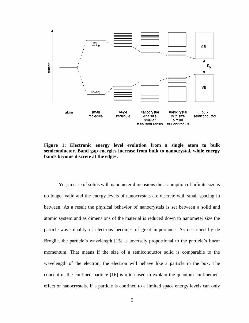
Figure 1 shows the transition of orbital energies from an atom to a solid.
Molecules are complex interacting arrangements of atoms that can be described by the
molecular orbital (MO) theory. Molecular orbitals are approximated by linear
combination of atomic orbitals (LCAO method) and the electron distribution in
molecules leads to the formation of bonding and anti-bonding orbitals [14]. These
orbitals have energies lower and higher than the isolated atoms, respectively. For
increasing molecular complexity a greater variety of molecular orbitals are formed. Yet,
for an infinite solid the energy spacing between the orbitals decreases so much that
discrete energy levels merge into continuous bands. The valence band in solids is derived
from the bonding orbital in molecules, while the conduction band results from the anti-
bonding orbitals.
5
Figure 1: Electronic energy level evolution from a single atom to bulk
semiconductor. Band gap energies increase from bulk to nanocrystal, while energy
bands become discrete at the edges.
Yet, in case of solids with nanometer dimensions the assumption of infinite size is
no longer valid and the energy levels of nanocrystals are discrete with small spacing in
between. As a result the physical behavior of nanocrystals is set between a solid and
atomic system and as dimensions of the material is reduced down to nanometer size the
particle-wave duality of electrons becomes of great importance. As described by de
Broglie, the particle‟s wavelength [15] is inversely proportional to the particle‟s linear
momentum. That means if the size of a semiconductor solid is comparable to the
wavelength of the electron, the electron will behave like a particle in the box. The
concept of the confined particle [16] is often used to explain the quantum confinement
effect of nanocrystals. If a particle is confined to a limited space energy levels can only
6
have discrete values that are determined by the mass of the particle and the dimensions of
the space. Hence the properties of charge carriers in semiconductor nanocrystals will
strongly depend on the size of the nanocrystal.
Photonic properties are also affected by particle size. If the incoming photon
matches the difference between two energy levels an exciton is generated, i.e. an excited
electron still bound to its hole through Coulombic interactions. The electron is orbiting
the hole analogous to an electron orbiting the nucleus in the hydrogen atom. The Bohr
radius of the exciton, based on the definition in the hydrogen atom, defines now the
minimum size of a nanocrystal, at which the exciton becomes spatially confined. For
example, for CdSe the Bohr radius is ~5.6 nm [17], i.e. for CdSe nanocrystals sizes
smaller than 11.2 nm the exciton assumes a state of higher kinetic energy. A
mathematical approach to explain the size dependence of electronic properties is the in
1986 by Brus [18] proposed effective mass model, which states that the minimum energy
Eg,nano that is required to generate a free electron-hole pair in a nanocrystal is made up of
two contributions to the bulk band gap Eg,bulk. The confinement energy Econf of the two
carriers as well as the Coulomb attraction ECoulomb between electron and hole are affecting
the band gap of the nanocrystal. The contribution of the confinement energy can be
expressed with the effective masses of electron me and hole mh as:
(
) Equation 1
7
The Coulombic attraction ECoulomb is expressed in consideration of the screening
of the carriers by the crystal
Equation 2
Therefore, the band gap of the nanoparticle can be described as
Equation 3
Inserting equations 1 and 2 into 3 the band gap of the nanocrystal can be express
in dependence of the radius r
(
)
Equation 4
Equation 4 is termed as the effective mass approximation and should only be used
as a first approximation [16]. It is important to mention that this model is not valid for
very small particle sizes and it does not consider effects such as surface traps or surface
reconstruction. Further improvements of the effective mass approximation led to more
sophisticated models [26, 27]. Yet, the model shows that with decreasing radius r the
energy of the lowest excited state (conduction bands minimum) increases and therefore
the band gap of the nanoparticle increases. As charge carriers are confined the kinetic
energy becomes quantized causing the transition of continuous bands to discrete energy
levels as shown in Figure 1, while the transition begins at the edge of the bands. This size
8
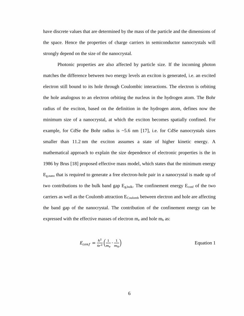
Figure 2: Surface to volume ratio vs. particle diameter. At a diameter below 10 nm
the surface to volume ratio increases rapidly.
dependence of the band gap makes nanoparticles with interesting optical properties
highly attractive for photovoltaic applications or light emitting diodes.
A second phenomenon of nanocrystalline material is the change of surface area to
volume ratio. In bulk surface atoms present a negligible portion of the total number of
atoms. However, as shown in Figure 2 with reduction of particle diameter the increase of
surface atoms becomes important at diameters below 10 nm. The high surface area to
volume ratio of nanoparticles has found application, e.g. in dye-sensitized solar cells
(DSSC), where strong light absorption by the dye is required in combination with an only
monolayer thin coverage of the electron transporting oxide. In nanoparticle/organic
hybrid solar cells high surface area to volume ratio is beneficial since a large interfacial
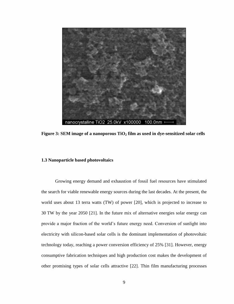
area is essential for efficient charge separation [19]. Figure 3 shows a nanoporous TiO2
film as used in DSSCs. Furthermore, with increasing surface atom exposure the presence
of surface states becomes important, since such can provide pathways for non-radiative
recombination of photogenerated charge carriers.
9
Figure 3: SEM image of a nanoporous TiO2 film as used in dye-sensitized solar cells
1.3 Nanoparticle based photovoltaics
Growing energy demand and exhaustion of fossil fuel resources have stimulated
the search for viable renewable energy sources during the last decades. At the present, the
world uses about 13 terra watts (TW) of power [20], which is projected to increase to
30 TW by the year 2050 [21]. In the future mix of alternative energies solar energy can
provide a major fraction of the world‟s future energy need. Conversion of sunlight into
electricity with silicon-based solar cells is the dominant implementation of photovoltaic
technology today, reaching a power conversion efficiency of 25% [31]. However, energy
consumptive fabrication techniques and high production cost makes the development of
other promising types of solar cells attractive [22]. Thin film manufacturing processes
10
have been a successful approach in fabricating low cost second generation photovoltaic
devices. Amorphous silicon, cadmium telluride (CdTe) and copper indium gallium
diselenide (CIGS) based cells with efficiencies of over 19% [31] are candidates for large-
scale production of solar modules. Third generation photovoltaic cells made of multi-
junctions aim at increasing electrical performance, while keeping production cost low.
Approaches containing inorganic nanorystalline material in combination with organic
molecules allow the departure from conventional solid state cells. Solution processability
in absence of high vacuum simplifies the preparation of such cells and reduces
manufacturing costs [33].
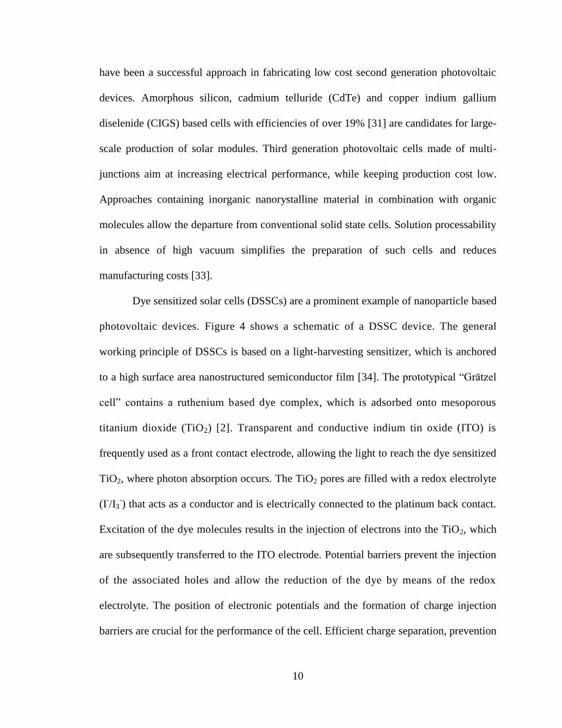
Dye sensitized solar cells (DSSCs) are a prominent example of nanoparticle based
photovoltaic devices. Figure 4 shows a schematic of a DSSC device. The general
working principle of DSSCs is based on a light-harvesting sensitizer, which is anchored
to a high surface area nanostructured semiconductor film [34]. The prototypical “Grätzel
cell” contains a ruthenium based dye complex, which is adsorbed onto mesoporous
titanium dioxide (TiO2) [2]. Transparent and conductive indium tin oxide (ITO) is
frequently used as a front contact electrode, allowing the light to reach the dye sensitized
TiO2, where photon absorption occurs. The TiO2 pores are filled with a redox electrolyte
(I-/I3
-) that acts as a conductor and is electrically connected to the platinum back contact.
Excitation of the dye molecules results in the injection of electrons into the TiO2, which
are subsequently transferred to the ITO electrode. Potential barriers prevent the injection
of the associated holes and allow the reduction of the dye by means of the redox
electrolyte. The position of electronic potentials and the formation of charge injection
barriers are crucial for the performance of the cell. Efficient charge separation, prevention
11
Figure 4: Operation principle of a dye-sensitized solar cell. The absorption of a
photon generates an excited dye molecule (dye*). The electron injection occurs into
the conduction band of the nanocrystalline TiO2 from where electrons diffuse to the
ITO front contact. The Pt back contact is being oxidized and the iodide/triiodide
mediator forms a regenerative cycle that donates electrons to the dye.
of recombination and stability of the device strongly depends on the electronic properties
of the interfaces present in the cell. The DSSC‟s power conversion efficiency of over
11% [35, 36] is competitive to amorphous and thin layer silicon photovoltaics.
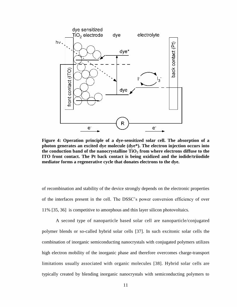
A second type of nanoparticle based solar cell are nanoparticle/conjugated
polymer blends or so-called hybrid solar cells [37]. In such excitonic solar cells the
combination of inorganic semiconducting nanocrystals with conjugated polymers utilizes
high electron mobility of the inorganic phase and therefore overcomes charge-transport
limitations usually associated with organic molecules [38]. Hybrid solar cells are
typically created by blending inorganic nanocrystals with semiconducting polymers to
12
Figure 5: Energy level diagram of an excitonic hetero-junction solar cell. The optical
band gap energy is less than the energy required to produce a free electron and hole
(electrical band gap). But the exciton created by light absorption dissociates into
separate charges at the interface, because the band offset between the two materials
provides an exothermic pathway for dissociation.
create a photo-active layer [6, 28] that can be deposited by spin-casting or layer by layer
deposition [39]. As a result of the blending step, the electron and hole conductor, such as
nanorystalline CdSe and poly-3(hexylthiophene) (P3HT) polymer form a bulk hetero-
junction, where both components are in intimate contact (Figure 5). In 1995 such hetero-
junction structures were first described independently by Halls et al. [23] and Yu et al.
[24]. Impinging photons generate electron-hole pairs, which separate into free charge
carries at the interface between the two semiconductors. Depending on the component‟s
electronic structure and resulting band offsets the efficiency of the charge separation is a
main contributor to the overall efficiency of the photovoltaic device. Since diffusion
lengths of generated excitons (Frenkel excitons) in conductive polymers are only in the
13
range of 5-15 nm [42-45], the interface density in the mixture must be high so that the
excitons have to diffuse only a short distance to the interface in order to achieve high
quantum efficiency for charge separation [25]. The efficiency of devices containing
inorganic nanocrystals mixed with a conductive polymer is currently about 3% [5].
Photovoltaic devices with these configurations contain a multitude of interfaces
between different components of the cell. Front contact, absorber material and back
contact are only the elemental components which in conjunction with each other create
the cycle for the transport of photo-generated carriers. A thorough investigation of the
electronic structure of such interfaces is an essential step on the way towards
understanding charge transport processes occurring within these cells. Improvement of
existing devices by enhancement of contacts or modification of internal structures is a
possible consequence of such investigations. In addition to the fundamental importance
of this study, understanding charge transfer dynamics is also crucial to the development
of new nanoparticle based devices, such as molecular electronics [26] or novel solar cells.
14
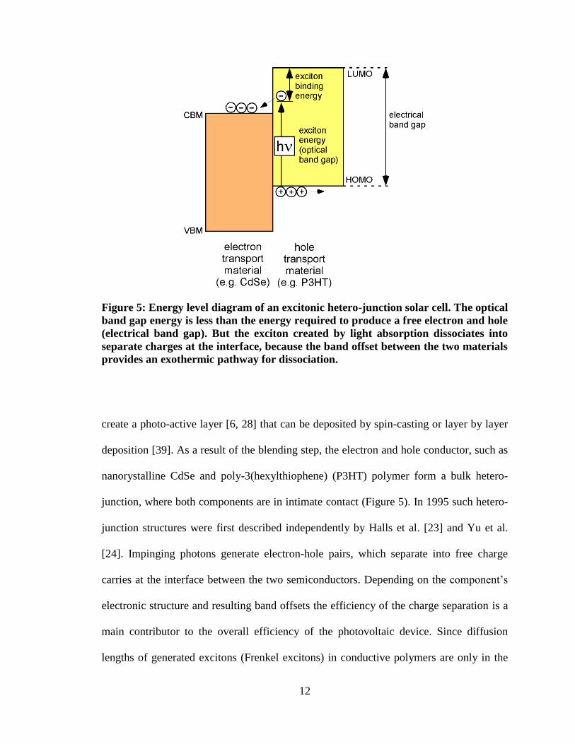
Figure 6: Semiconductor band structure, (a) flat band situation, (b) surface band
bending, (c) presence of a positive surface dipole
1.4 Semiconductor surface and interface electronic structures
The main focus of this study is the determination of the electronic structure of
semiconducting nanocrystalline surfaces and interfaces. Typically, electronic properties
of semiconductors are illustrated in band diagrams. As shown in Figure 6 (a), this type of
depiction shows vacuum level (Evac), valence bands maximum (EVB) and conduction
bands minimum (ECB) as a function of distance. In comparison to a metal,
semiconductors exhibit an absence of electronic states around the Fermi level (EF).
Therefore, in semiconductors the work function (Φ) is not equivalent to the electron
affinity (χ) and ionization energy (Eion). The work function is defined as the energy
separation between the vacuum level and the Fermi level. The electron affinity is defined
as the difference between CBM and vacuum level and the ionization energy is the
15
difference between VBM and vacuum level. The bulk electronic properties of
semiconductors are often different than electronic properties at the surface. Due to the
presence of surface defects the formation of surface states can introduce a change of the
Fermi level and cause surface band bending. As shown in Figure 6 (b), since the Fermi
level is shifted relative to the band edges and the vacuum level the work function changes,
while ionization energy and electron affinity remain constant. Variation of the vacuum
level without a change of the Fermi level is a result of the formation of a surface dipole (δ)
(Figure 6 (c)), which can be caused by different surface terminations, such as
electropositive or electronegative adsorbates [27, 28], structural surface changes or even
photochemical surface modifications [51]. A negative surface charge causes an increase
of the surface dipole and a positive surface charge causes a decrease of the surface dipole,
i.e. a work function reduction.
Upon contact of two semiconductors the materials form a semiconductor hetero-
interface and the energy bands align to accommodate the difference in electron affinity.
Modulation of band structures across such interfaces are based on the electron affinity
rule, which states that for construction of a band diagram the vacuum level of both
semiconductors should be aligned. In 1939 Schottky developed the foundation and
described the determination of band offsets at metal/semiconductor interfaces [29, 30]. In
1962 this model was then improved by Anderson and can be applied to semiconductor
hetero-interfaces [31]. As the alignment depends on the vacuum level alignment
conduction and valence bands experience an offset, often termed as charge injection
barriers. Upon photo-excitation of an electron from the valence band into the conduction
band electrons are free to move within the conduction band. Therefore, conduction band
16
Figure 7: Formation of a semiconductor hetero-interface. (a) shows the two
semiconductors before contact. After thermodynamic equilibrium is reached (b) the
Fermi levels are aligned and a surface dipole δ is formed.
offsets (ΔECB) refer to the electron injection barriers and valence band offsets (ΔEVB) to
the hole injection barrier (Figure 7). According to the Anderson model band offsets are a
result of bulk properties of the semiconductors and physico-chemical phenomena are not
considered. Yet, due to charge transfer into electronic states localized at the interface the
formation of an interface dipole (δ) is usually observed. Therefore, predictions of the
Schottky and Anderson model do not apply to most real hetero-junctions because
interface dipoles are not considered. If interface states would occur within the band gap
they would result in Fermi level pinning, while interface states outside the band gap
would cause the formation of dipoles and therefore an offset at the vacuum level. Hence,
the predicted alignments need to be verified experimentally in order to determine realistic
interfacial band line-ups and understand the mechanistics of the barrier height formation.
17
Figure 8: Possible factors causing an interface or surface dipole. (a) charge transfer
across the interface, (b) adsorbate leads to an image charge effect at the surface, (c)
rearrangement of the surface and reduction of tailing of the electron cloud into the
vacuum by repulsion with the electron cloud in the adsorbate, (d) surface dipole
caused by chemical interaction, (e) existence of interface states buffers charge
carriers, and (f) orientation of a polar molecule. (cf. Ref. [55])
Only during recent years, organic/inorganic semiconductor interfaces have
received greater attention [56-60] especially due to their potential as photoactive hetero-
junctions in hybrid photovoltaics [5]. Similar to the behavior at organic-on-metal
interfaces it was found that most interfacial band alignments [56] do not follow the
electron affinity rule due to physico-chemical interactions at the interface and the
resulting formation of dipoles. For organic semiconductors on metals the formation of
dipole barriers > 1 eV [55, 61] have been observed. The characteristics of the interfacial
band alignment of organic material on semiconductors do not differ significantly from the
18
interface formation of organic material on metals. Generally, most dipole inducing effects
are caused by physisorption or chemisorption effects. Ishii et al. [55] have summarized
the contributing factors: As shown in Figure 8 (a) the formation of a dipole layer can be
caused by electron transfer across the interface. The image effect is shown in (b), where
the concentration of electrons in the organic material leads to a positive charging of the
vacuum side. The “push-back” effect is shown in (c), where the spill-out of electron
density into the vacuum is reduced through charge redistribution by Pauli-repulsion.
Another factor for dipole formation is the effect of chemical interactions or new bond
formation (d) as well as the presence of interface states (e). The latter is commonly
observed in inorganic semiconductors [62], e.g. due to the presence of oxygen vacancies.
In (f) the formation of a permanent dipole is caused by orientation of polar molecules or
the presence of functional groups.
In the present study, dipole formation due to UV-induced surface modification
will be discussed on nanocrystalline metal oxide surfaces and observed work function
reductions will be related to surface dipole formation. The ITO/TiO2 semiconductor
hetero-interface found in DSSCs will be investigated and results will be discussed with
regard to changes of charge injection barriers induced by UV radiation.
19
CHAPTER 2: EXPERIMENTAL METHODOLOGY
2.1 Electrospray technique
2.1.1 Electrospray for thin film deposition
The application of macromolecular or nanocrystalline material for a variety of
electric devices requires the formation of two- or three-dimensional structures.
Traditionally, these structures are formed by simple spin-coating, dip-coating or even
ink-jet printing [32-34] on a substrate in ambient atmosphere or by vapor deposition in
high vacuum [35, 36]. These deposition techniques have limitations with regard to thin
film deposition for surface science experiments on macromolecular materials. For
example, solution processing in air is a quick and easy approach of preparing a thin film
of macromolecules, but the cleanness of the surface has to be compromised as
environmental contamination is inevitably introduced [37, 38]. Thin film formation of
macromolecular material by evaporation in vacuum is difficult, due to the high molecular
weight and fragility of the organic material, which often results in the dissociation of the
deposited material [35, 39]. Photoemission spectroscopy experiments, however, require
the absence of contamination [27], making a deposition approach necessary which
provides macromolecular surfaces without contamination.
20
A solution to this challenge is electrospray deposition. It permits the injection of
(conductive) polymers [40-43], nanocrystalline material [44, 45], biomolecules [46], even
living cells and organisms [47] and other macromolecular material from solution into
vacuum. In this “gentle technique” the solution containing the material of interest is
nebulized from a syringe by application of high voltage. The produced aerosol is drawn
through an intake orifice into the vacuum chamber and onto a substrate. During flight the
droplets evaporate and the solute is deposited on the substrate. The technique is based on
the well-established electrospray ionization mass spectrometry (ESIMS) method, which
was developed by Fenn and co-workers in the 1980s [48]. In ESIMS, large molecules
(e.g. proteins) are put in the gas phase so that they can be characterized by their mass to
charge ratio. The integration of this method into a multi-chamber photoemission
spectroscopy setup as deposition technique allows the characterization of interfaces with
photoemission spectroscopy in combination with in-vacuum multi-step deposition. The
deposition control is similar to thermal evaporation in vacuum, i.e. film thickness can be
controlled with sub-monolayer accuracy [49].
21
Figure 9: Schematic of the electrospray deposition process. A strong electric field
creates ionized droplets, which contain the to-be-deposited particles. Coulomb
explosions separate solvent molecules from the particles and the solvent is extracted
in the pumps. In a final step the particles enter the preparation chamber and form a
thin film.
2.1.2 Physical principle
Figure 9 shows a schematic of the electrospray process. The solution (usually in
the mg/ml concentration range) is prepared in atmosphere and loaded into a capillary.
The capillary tip is made of metal, which permits the application of a high voltage
between capillary and substrate. Due to the strong electric field molecules present in the
solution ionize. Anions (in negative voltage mode) will be accelerated and cations will
migrate away from the capillary tip. As a result of the potential difference between
22
capillary tip and sample the liquid accelerates towards the substrate. At the apex of the
capillary a Taylor-cone [50] emerges at whose apex a jet effuses, which breaks up and
forms a three dimensional plume of charged droplets. The external field extracted
droplets from the Taylor-cone are charged containing an imbalance of solute and counter
ions. In order to prevent entry of ambient contamination, capillary and orifice are usually
enclosed and flooded with high purity N2 gas. As the charged droplets are carried through
the differential pumping stages solvent molecules evaporate and droplets shrink. The
charge density increases during this process, and the Coulombic forces can overcome the
surface tension at some point at which “Coulomb explosions” occur. This furthermore
separates solute from solvent molecules and in the end a solute beam impinges on the
substrate, forming a thin film of the solute molecules.
2.2 Photoemission spectroscopy
Photoemission spectroscopy (PES) is a surface sensitive characterization
technique that enables the probing of occupied states of solids or molecules. In 1887
Hertz [51] was among the first to discover and in 1905 Einstein [52] the first to describe
the photoelectric effect - the founding principle of PES. This phenomenon was applied in
a high resolution photoelectron spectrometer invented by Siegbahn and co-workers in the
1950s [53]. The improvement of the resolution to below 1 eV enabled the detection of
elements and chemical shifts in the electron binding energies giving rise to “ESCA”
(electron spectroscopy for chemical analysis) [54, 55].
23
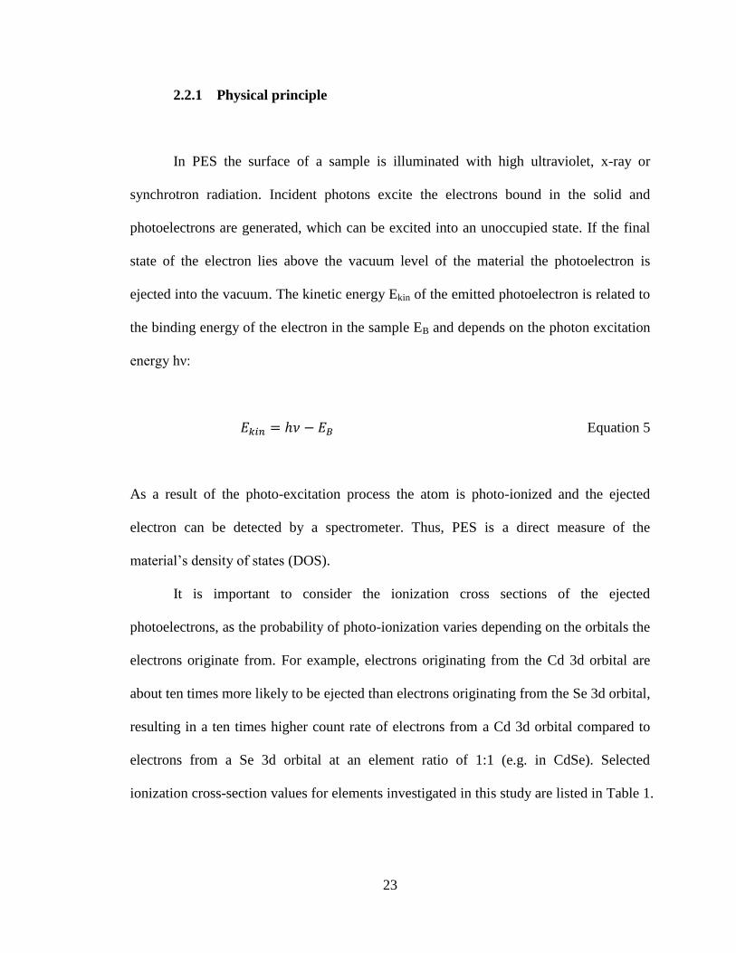
2.2.1 Physical principle
In PES the surface of a sample is illuminated with high ultraviolet, x-ray or
synchrotron radiation. Incident photons excite the electrons bound in the solid and
photoelectrons are generated, which can be excited into an unoccupied state. If the final
state of the electron lies above the vacuum level of the material the photoelectron is
ejected into the vacuum. The kinetic energy Ekin of the emitted photoelectron is related to
the binding energy of the electron in the sample EB and depends on the photon excitation
energy hν:
Equation 5
As a result of the photo-excitation process the atom is photo-ionized and the ejected
electron can be detected by a spectrometer. Thus, PES is a direct measure of the
material‟s density of states (DOS).
It is important to consider the ionization cross sections of the ejected
photoelectrons, as the probability of photo-ionization varies depending on the orbitals the
electrons originate from. For example, electrons originating from the Cd 3d orbital are
about ten times more likely to be ejected than electrons originating from the Se 3d orbital,
resulting in a ten times higher count rate of electrons from a Cd 3d orbital compared to
electrons from a Se 3d orbital at an element ratio of 1:1 (e.g. in CdSe). Selected
ionization cross-section values for elements investigated in this study are listed in Table 1.
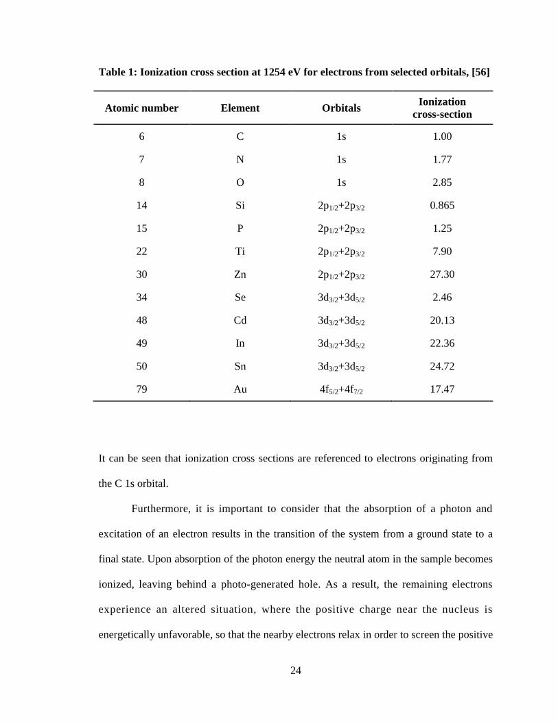
24
Table 1: Ionization cross section at 1254 eV for electrons from selected orbitals, [56]
Atomic number Element Orbitals Ionization
cross-section
6 C 1s 1.00
7 N 1s 1.77
8 O 1s 2.85
14 Si 2p1/2+2p3/2 0.865
15 P 2p1/2+2p3/2 1.25
22 Ti 2p1/2+2p3/2 7.90
30 Zn 2p1/2+2p3/2 27.30
34 Se 3d3/2+3d5/2 2.46
48 Cd 3d3/2+3d5/2 20.13
49 In 3d3/2+3d5/2 22.36
50 Sn 3d3/2+3d5/2 24.72
79 Au 4f5/2+4f7/2 17.47
It can be seen that ionization cross sections are referenced to electrons originating from
the C 1s orbital.
Furthermore, it is important to consider that the absorption of a photon and
excitation of an electron results in the transition of the system from a ground state to a
final state. Upon absorption of the photon energy the neutral atom in the sample becomes
ionized, leaving behind a photo-generated hole. As a result, the remaining electrons
experience an altered situation, where the positive charge near the nucleus is
energetically unfavorable, so that the nearby electrons relax in order to screen the positive
25
Figure 10: Universal curve of inelastic mean free path (λ) as a function of the
electron’s kinetic energy. The curve has a minimum between 50-70 eV. (cf. Ref. [57])
charges from each other (image charge screening). Because the photoemission process is
about one magnitude slower than the relaxation process, photoemission spectroscopy is
sensitive to such final state effects. The polarization energy is a negative contribution to
the binding energy of detected electrons [58].
Even though the penetration depth of the incident photons is in the order of tens
of µm, the average distance an electron can travel within a material before it is
inelastically scattered (inelastic mean free path λ) is only in the range of a few tens of Å.
As Figure 10 shows, the empirically determined values of λ are a function of the kinetic
energy of the electrons, but λ is rather independent of material composition.
26
Figure 11: Probability of an electron travelling the distance d vs. (d/ λ) shows that
most detected photoelectrons originate from a depth of about 3λ.
Since λ can be described as the probability of an electron travelling a distance d
without undergoing scattering
( )
Equation 6
most electrons probed originate from about 3λ (see Figure 11) below the solid surface of
the sample, making photoemission spectroscopy a very surface sensitive characterization
technique. If the photo-excited electron undergoes inelastic scattering on its way to the
sample surface the electronic signature of the orbital where it comes from is lost. These
types of electrons are considered secondary electrons and contribute to the background
signal in photoemission spectroscopy.
27
2.2.2 Instrumentation
Traditionally, excitation sources used for PES are x-ray tubes for x-ray
photoemission spectroscopy (XPS) and gas discharge lamps for ultraviolet photoemission
spectroscopy (UPS). An electron beam of several keV striking a magnesium anode
provides a characteristic x-ray radiation Mg Kα1,2 at fixed photon energy of 1253.6 eV
superimposed on a bremsstrahlung background. Using the He Iα line of a helium
discharge lamp allows UPS measurements with an excitation energy of 21.21 eV.
Furthermore it is important to mention that synchrotron radiation in conjunction with a
monochromator can be used, providing a broad spectral range. As mention in Section
2.2.1 the absorption of a photon generates an excited electron. The use of a concentric
hemispheric analyzer in conjunction with a retarding lens system enables the detection of
the photoelectrons. An electron multiplier is then used to detect the energy-selected
electrons [27].
Usually the Fermi level is defined to have a binding energy of 0 eV. Since sample
and spectrometer are electrically connected, their Fermi energies are equilibrated. Figure
12 shows the energy level diagram for the photoelectron detection by the spectrometer.
The kinetic energy of the photoelectron in vacuum is given by
Equation 7
where Φsample is the work function of the sample. As it is illustrated in Figure 12,
work functions of sample and spectrometer are different. Hence, the photoelectron has to
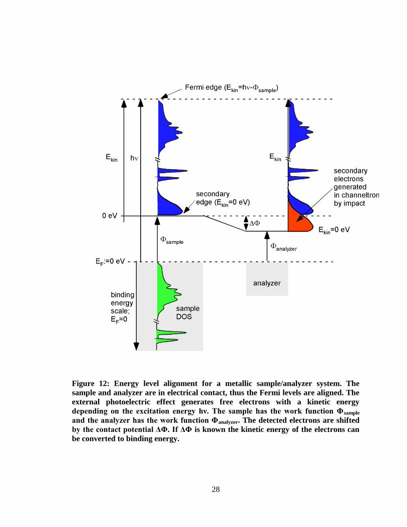
28
Figure 12: Energy level alignment for a metallic sample/analyzer system. The
sample and analyzer are in electrical contact, thus the Fermi levels are aligned. The
external photoelectric effect generates free electrons with a kinetic energy
depending on the excitation energy hν. The sample has the work function Φsample
and the analyzer has the work function Φanalyzer. The detected electrons are shifted
by the contact potential ΔΦ. If ΔΦ is known the kinetic energy of the electrons can
be converted to binding energy.
29
overcome this contact potential difference (Φsample – Φanalyzer) in order to be detected. The
kinetic energy of the photoelectron changes on its way from sample to spectrometer:
( ) Equation 8
As a result, the determined binding energy becomes independent of the sample work
function. Equation 9 describes the kinetic energy of a photoelectron in the spectrometer
in reference to the Fermi energy:
Equation 9
Since Fermi levels are equilibrated, kinetic energy values can be converted to binding
energies if Φanalyzer is known. The sample work function Φsample is not required for this
conversion. As it will be described in Section 2.2.4 it can be determined by the secondary
electron cutoff usually measured with UPS. Typically, an accelerating potential (bias
voltage) is applied to separate the secondary electrons originating from the sample and
the secondary electrons generated by the analyzer.
2.2.3 X-ray photoemission spectroscopy (XPS)
The excitation of electrons with x-rays, e.g. Mg Kα1,2 (1253.6 eV), enables the
probing of core-level electrons. The main purpose of XPS measurements is the
determination of the elemental composition, which can be identified by plotting the
30
Figure 13: Characteristic photoemission spectrum of polycrystalline gold. Emission
features with highest intensities are usually used for further studies, such as Au 4f
orbital features.
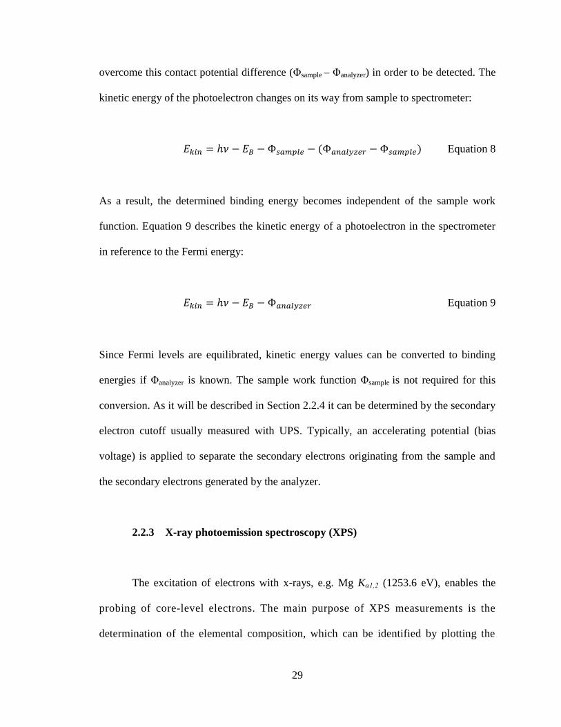
photoelectron intensity vs. binding energy. Figure 13 shows an exemplary survey
spectrum measured on an Ar+ sputter cleaned Au surface. The resulting emission features
are characteristic for Au.
Chemical shifts of core levels are caused by a change in local bonding
environment. The direction of these shifts depends on attractive potential of the nucleus
and the repulsive interaction with the surrounding electrons in the material. For example,
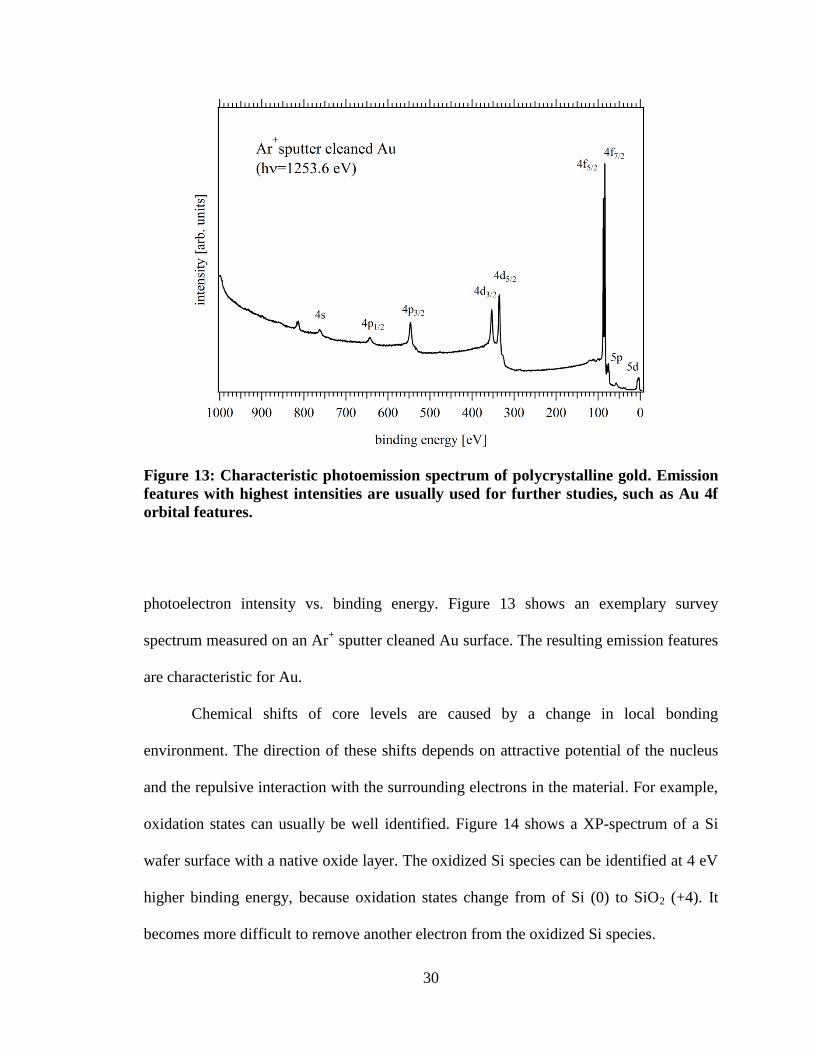
oxidation states can usually be well identified. Figure 14 shows a XP-spectrum of a Si
wafer surface with a native oxide layer. The oxidized Si species can be identified at 4 eV
higher binding energy, because oxidation states change from of Si (0) to SiO2 (+4). It
becomes more difficult to remove another electron from the oxidized Si species.
31
Figure 14: High resolution photoemission spectrum of Si with an additional Si 2p
peak caused by the native SiO2 layer.
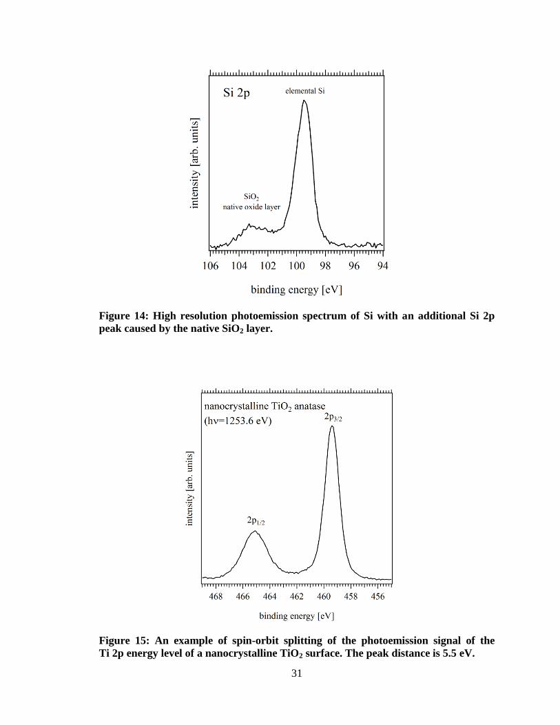
Figure 15: An example of spin-orbit splitting of the photoemission signal of the
Ti 2p energy level of a nanocrystalline TiO2 surface. The peak distance is 5.5 eV.
32
Core-level emission features can also be used to determine the thickness of an
overlayer grown on a substrate. Since electrons originating from the underlying substrate
need to penetrate the overlayer, scattering probability increases and the core-level
intensity is reduced. The overlayer thickness d can be calculated using the Lambert-Beer
law
(
) Equation 10
where I is the intensity of the covered substrate core-level peak and I0 is the initial
intensity of the substrate core-level peak before it was covered. λ is the inelastic mean
free path, which depends on the kinetic energy of the photoelectrons originating from the
core-level.
XPS core level data also enables the compositional analysis of a material. The
composition can be identified by comparing peak areas of elements present in a sample.
Yet, in order to determine correct peak areas the emission background should be removed
at first. The peak area AA is proportional to the amount of element A in the material. In
consideration of the ionization cross section S (see Section 2.2.1) the composition of a
sample can be expressed as a ratio of number of atoms of element A:B:
Equation 11
As already mentioned in Section 2.2.1 PES is considered a final state spectroscopy,
i.e. the photoelectron spectrum defined by the initial state is altered by final state effects.
33
Final states may cause energetic shifts, splitting or appearance of satellite peaks. Besides
the polarization effects mentioned above multiplet splitting is a final state artifact
apparent in photoemission spectra. Due to the interaction between the electron spin and
its motion (spin-orbit-coupling) the removal of an electron leaves the ion in different
electronic configurations depending on the spin of the removed electron. Therefore, for
photoemission peaks are split for electrons originating from p, d and f orbitals, with
intensity ratios of 1:2, 2:3 and 3:4, respectively. An example is shown in Figure 15,
where the Ti 2p emission peak is split into a 2p1/2 and a 2p3/2 peak with a ratio of 1:2.
2.2.4 Ultraviolet photoemission spectroscopy (UPS)
UPS measurements are conducted with lower energetic UV radiation, such as
He Iα (21.2182 eV), which probes shallow valence bands, i.e. electrons originating from
the outer shell with low binding energies (0-10 eV). Of course, these electrons can be
detected with XPS as well, but the line width of an atomic transition in the gas phase is
only about 10 meV, i.e. valence band structures measured with UPS are much higher
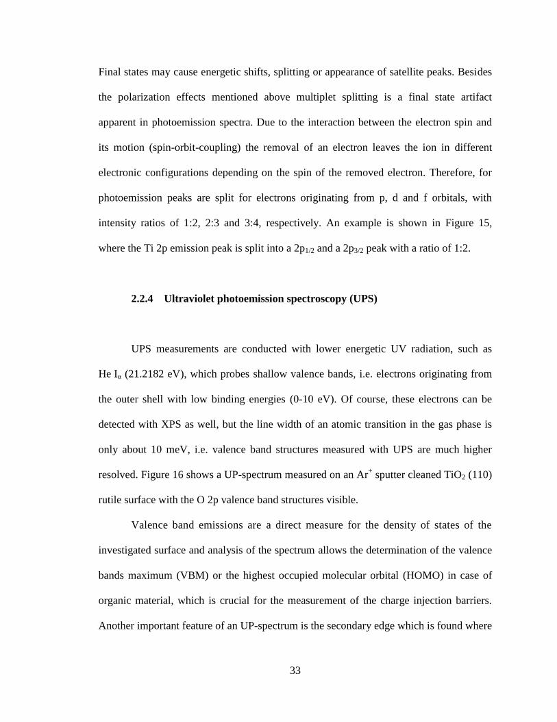
resolved. Figure 16 shows a UP-spectrum measured on an Ar+ sputter cleaned TiO2 (110)
rutile surface with the O 2p valence band structures visible.
Valence band emissions are a direct measure for the density of states of the
investigated surface and analysis of the spectrum allows the determination of the valence
bands maximum (VBM) or the highest occupied molecular orbital (HOMO) in case of
organic material, which is crucial for the measurement of the charge injection barriers.
Another important feature of an UP-spectrum is the secondary edge which is found where
34
Figure 16: Characteristic UP-spectrum of a TiO2 (110) rutile single crystal. A UP-
spectrum features the secondary edge and enables the determination of the surface
work function.
the secondary electron intensity decreases sharply. At this point, scattered secondary
electrons have barely enough energy to escape from the surface, i.e. the secondary
electron cutoff (Ekin = 0 eV) allows the determination of the work function of the surface.
Since the Fermi energy is defined as EB=0 eV the work function is defined as the energy
difference between the Fermi energy and the vacuum level [28]. The work function
depends on a variety of factors, such as surface roughness, surface dipoles or the presence
of adsorbates [28]. The adsorption of molecules can attenuate the signal of detected
valence electrons, as the very short mean free path of the electrons leads to broadening of
35
otherwise sharp features. Therefore, it might be necessary to prepare surfaces with
various cleaning methods, such as Ar+ sputtering, cleaving or annealing at elevated
temperatures. This is one of the reasons why ultra high vacuum (UHV) is necessary for
surface work. The time τc it takes to cover a surface with a monolayer of adsorbed
molecules is given by [27]:
Equation 12
where p is the gas pressure in mbar and s is the sticking coefficient, i.e. the
adsorption probability. In practice it means that in order to keep a surface clean for 1 h
and therefore accessible for surface sensitive UPS measurements a vacuum of 10-10
mbar
is necessary.
In contrast to Kelvin probe measurements (which only yield the contact potential
difference between sample and probe) UPS is able to deliver absolute work function
values. But there are two major sources of artifacts to be considered in UPS work
function measurements: (1) the build-up of positive charge during the measurement due
to incomplete replenishment of the emitted photoelectrons, and (2) the occurrence of
photochemical modification of the sample surface due to the impinging UV radiation.
Both artifacts result in a shift of the secondary electron cutoff to higher binding energy
and can therefore significantly alter the outcome of the work function measurement. Yet,
as both artifacts occur instantaneous upon UV exposure during a UPS measurement their
detection is challenging. Charging related effects are usually simpler to detect since the
shift of emission features is found across the complete spectral range, while
36
photochemical modifications require the use of low-intensity x-ray photoemission
spectroscopy (LIXPS), which enables a measurement of the secondary electron cutoff
before UPS due to its low dose of radiation.
2.2.5 Low intensity x-ray photoemission spectroscopy (LIXPS)
LIXPS was developed to determine photochemical surface modifications, which
result in changes of the surface work function. It was first used to determine the true
work function of an environmentally contaminated ITO surface [59]. LIXPS
measurements revealed that accurate work functions can be measured with a decreased
intensity of radiation, which in contrast to UPS measurements does not result in a change
of work function due to the radiation itself. Usually, LIXPS is used prior to the actual
UPS measurement in order to determine a pre-UPS work function value. If the surface of
interest is prone to high intensity photon flux (UV or x-rays) the work function will
decrease instantaneously upon conducting the UPS measurement. LIXPS uses
magnitudes less radiation intensity than a commercial UV light source. As a result it can
be used to determine charging or radiation induced photochemical surface modifications.
X-ray radiation used in LIXPS has enough intensity to resolve the secondary edge, yet
has not enough flux to measure core levels. In an experiment by Beerbom et al. [60], it
was shown with Kelvin probe measurements, that work functions measured with LIXPS
reveal the accurate surface work function. In this experiment the work function of a
solvent-cleaned ITO surface was measured with LIXPS and Kelvin probe before
exposing the surface to UV radiation during the UPS measurement. In a second step the
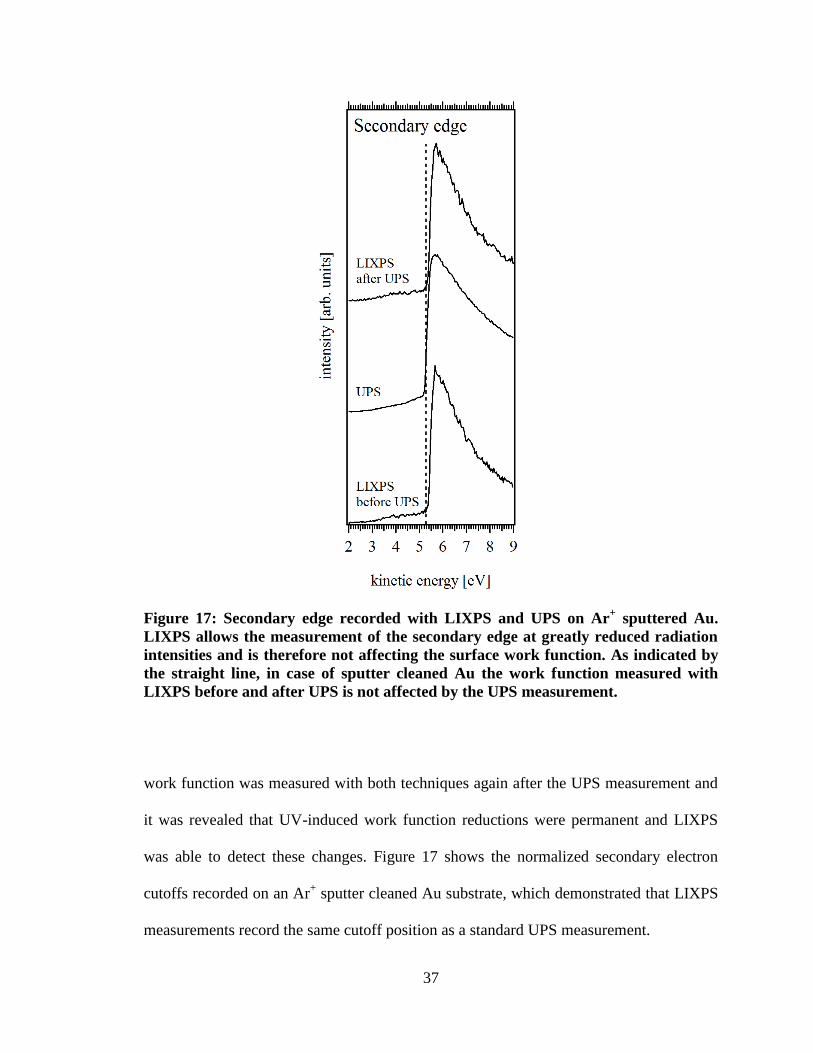
37
Figure 17: Secondary edge recorded with LIXPS and UPS on Ar+ sputtered Au.
LIXPS allows the measurement of the secondary edge at greatly reduced radiation
intensities and is therefore not affecting the surface work function. As indicated by
the straight line, in case of sputter cleaned Au the work function measured with
LIXPS before and after UPS is not affected by the UPS measurement.
work function was measured with both techniques again after the UPS measurement and
it was revealed that UV-induced work function reductions were permanent and LIXPS
was able to detect these changes. Figure 17 shows the normalized secondary electron
cutoffs recorded on an Ar+ sputter cleaned Au substrate, which demonstrated that LIXPS
measurements record the same cutoff position as a standard UPS measurement.
38
2.3 Optical absorption spectroscopy
Electronic excitations of electrons from filled bands to empty bands are typically
induced by electromagnetic radiation in the UV and visible light range (UV-Vis
spectroscopy). Wavelengths of these types of radiation are on the order of 200 to 800 nm.
With the Planck constant h and the speed of light c, the wavelength λ can be converted
into excitation energy of about 6.2 to 1.5 eV:
Equation 13
Depending on the energy gap between VBM (HOMO, respectively) and CBM
(LUMO, respectively) photons with wavelengths too long to excite an electron into the
empty bands will pass through, while photons with sufficient amounts of energy will be
absorbed and based on the electronic selection rules create an electron in the excited state.
UV-Vis spectroscopy is therefore suitable to determine important information about the
electronic structure and can be used to estimate band gap values.
After the excitation of an electron from a ground state S0 the electron density and
therefore equilibrium geometry changes and the electron is transitioned into an
electronically and vibrationally excited state S1. Most transitions are so-called Franck-
Condon transitions, where the transition happens vertically, because the electronic
transition is completed before the nucleus can alter its spatial position. The Franck-
Condon principle describes spectroscopic transition and relaxation as simultaneous. In a
39
non-vertical transition the nucleus position is different from the ground state position,
i.e.the lattice had time to relax.
In a typical absorption spectrum the absorbance A is plotted versus the
wavelength of the incoming photons. Since A is defined as
Equation 14
where I0 is the photon intensity before absorption and I is the photon intensity
after absorption, an absorbance < 1 means that photons have successfully excited
electrons into the unoccupied band. After the excitation to the upper vibronic state in the
first excited state S1 the electron relaxes radiationless to the lowest vibrational state and
finally returns to the ground state S0 by emitting a photon, which results in a fluorescence
band.
As discussed in Section 2.2.3 the polarization of a molecule upon photo-excitation
causes the orbital left behind to change its shape and the remaining electrons feel
Coulomb attraction to the vacant hole. This final state of a positive ion in its
electronically polarized surrounding is measured with PES. In comparison to a molecular
ion in the gas phase the ionization energy Eion is reduced by P+, while the electron affinity
EA is increased by P-. As shown in Figure 19 the HOMO (VBM) and LUMO (CBM)
levels are shifted due to the electronic polarization and the energy that is necessary to
create this well-separated pair of ions in the crystal is the transfer gap E transfer. The
transfer gap can be determined with inverse photoemission spectroscopy (IPES) in
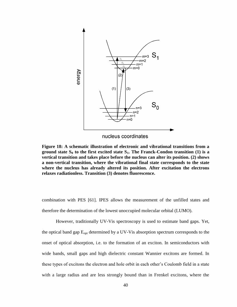
40
Figure 18: A schematic illustration of electronic and vibrational transitions from a
ground state S0 to the first excited state S1. The Franck-Condon transition (1) is a
vertical transition and takes place before the nucleus can alter its position. (2) shows
a non-vertical transition, where the vibrational final state corresponds to the state
where the nucleus has already altered its position. After excitation the electrons
relaxes radiationless. Transition (3) denotes fluorescence.
combination with PES [61]. IPES allows the measurement of the unfilled states and
therefore the determination of the lowest unoccupied molecular orbital (LUMO).
However, traditionally UV-Vis spectroscopy is used to estimate band gaps. Yet,
the optical band gap Eopt determined by a UV-Vis absorption spectrum corresponds to the
onset of optical absorption, i.e. to the formation of an exciton. In semiconductors with
wide bands, small gaps and high dielectric constant Wannier excitons are formed. In
these types of excitons the electron and hole orbit in each other‟s Coulomb field in a state
with a large radius and are less strongly bound than in Frenkel excitons, where the
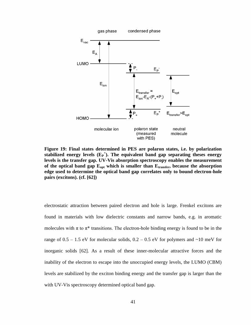
41
Figure 19: Final states determined in PES are polaron states, i.e. by polarization
stabilized energy levels (EP+). The equivalent band gap separating theses energy
levels is the transfer gap. UV-Vis absorption spectroscopy enables the measurement
of the optical band gap Eopt which is smaller than Etransfer, because the absorption
edge used to determine the optical band gap correlates only to bound electron-hole
pairs (excitons). (cf. [62])
electrostatic attraction between paired electron and hole is large. Frenkel excitons are
found in materials with low dielectric constants and narrow bands, e.g. in aromatic
molecules with π to π* transitions. The electron-hole binding energy is found to be in the
range of 0.5 – 1.5 eV for molecular solids, 0.2 – 0.5 eV for polymers and ~10 meV for
inorganic solids [62]. As a result of these inner-molecular attractive forces and the
inability of the electron to escape into the unoccupied energy levels, the LUMO (CBM)
levels are stabilized by the exciton binding energy and the transfer gap is larger than the
with UV-Vis spectroscopy determined optical band gap.
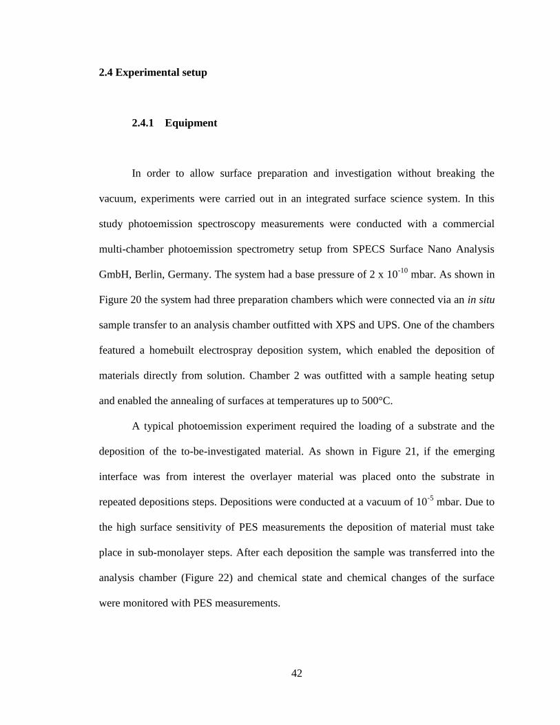
42
2.4 Experimental setup
2.4.1 Equipment
In order to allow surface preparation and investigation without breaking the
vacuum, experiments were carried out in an integrated surface science system. In this
study photoemission spectroscopy measurements were conducted with a commercial
multi-chamber photoemission spectrometry setup from SPECS Surface Nano Analysis
GmbH, Berlin, Germany. The system had a base pressure of 2 x 10⁻¹⁰
mbar. As shown in
Figure 20 the system had three preparation chambers which were connected via an in situ
sample transfer to an analysis chamber outfitted with XPS and UPS. One of the chambers
featured a homebuilt electrospray deposition system, which enabled the deposition of
materials directly from solution. Chamber 2 was outfitted with a sample heating setup
and enabled the annealing of surfaces at temperatures up to 500°C.
A typical photoemission experiment required the loading of a substrate and the
deposition of the to-be-investigated material. As shown in Figure 21, if the emerging
interface was from interest the overlayer material was placed onto the substrate in
repeated depositions steps. Depositions were conducted at a vacuum of 10-5
mbar. Due to
the high surface sensitivity of PES measurements the deposition of material must take
place in sub-monolayer steps. After each deposition the sample was transferred into the
analysis chamber (Figure 22) and chemical state and chemical changes of the surface
were monitored with PES measurements.
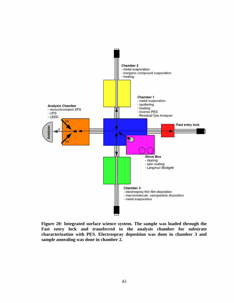
43
Figure 20: Integrated surface science system. The sample was loaded through the
Fast entry lock and transferred to the analysis chamber for substrate
characterization with PES. Electrospray deposition was done in chamber 3 and
sample annealing was done in chamber 2.
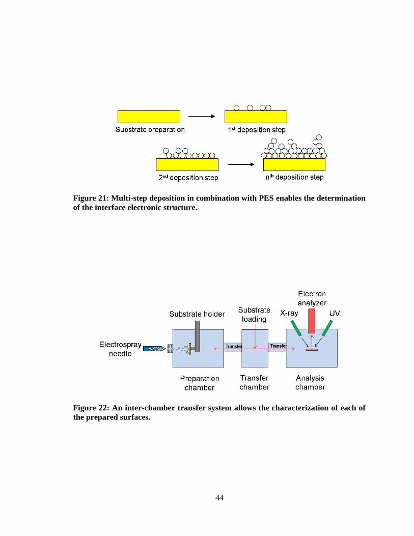
44
Figure 21: Multi-step deposition in combination with PES enables the determination
of the interface electronic structure.
Figure 22: An inter-chamber transfer system allows the characterization of each of
the prepared surfaces.
45
For the electrospray deposition step, a Keithley high voltage power supply (248)
was used to apply -2 kV. A Cole-Parmer syringe pump (WU-74900-00) was used at a
pumping speed of 4 ml/h. Hamilton stainless steel cone tip needles (7785-01) and
Hamilton syringes (22194-U) with a volume of 5 ml were purchased from Sigma Aldrich.
An x-ray source XR50 and UV source UVS 10/35 was used for photon generation and a
hemispherical energy analyzer PHOIBOS 100 was used for photoelectron detection. A
Thuramed spectrophotometer T60-U was used for absorption spectroscopy studies.
2.4.2 Sample preparation
The particular substrates used in the discussed studies are mentioned in the
individual chapters and sections. In general, substrates were glued on a custom made
substrate holder with a conductive silver epoxy or screwed on with an electrical contact
established via the screw heads. The latter attachment method allowed sample annealing.
Silicon wafers were purchased from Wacker Chemie (Munich, Germany) and
etched in 10% HF solution for 8 s, rinsed and etched for an additional 3 s and
immediately loaded into the vacuum chamber. Subsequent Ar+ sputter cleaning removed
residual SiO2 and adsorbates. Au coated Si wafers were prepared by depositing Ti and Au
by electron beam evaporation. The samples were sonication in acetone, methanol and iso-
propanol for 5 min each, dried in a stream of nitrogen and subsequently Ar+ sputter
cleaned. Indium tin oxide (ITO) coated glass slides were purchased from Thin Film
Devices Inc. (Anaheim, CA). The manufacturer reports an ITO thickness of 150 nm. The
substrates were sonicated in acetone, methanol and iso-propanol for 5 min each, dried in
46
a stream of N2 and subsequently Ar+ sputter cleaned. Highly ordered pyrolytic graphite
(HOPG) crystal substrates (Mikromasch, USA, “ZYA” quality) were cleaved to obtain a
pristine surface. The crystals were attached to the substrate holder via conductive silver
epoxy and a thin metal sheet was attached to the top of the HOPG crystal. After loading
the sample, a manipulator arm was used to remove the foil along with the top layer of the
crystals, creating a clean graphite surface. All substrates were characterized by LIXPS,
UPS and XPS before further experimental steps were taken.
TiO2 nanoparticles were purchased as Ti-Nanoxide HT-L from Solaronix
(Aubonne, Switzerland). According to the manufacturer the average particle size of the
nanoparticles is 9 nm. TiO2 nanoparticles were dispersed in a 1:1 ethanol:water mixture
to create a dispersion with a concentration of 5 mg/ml. ZnO nanoparticles were purchased
from Alfa Aesar (Nanophase Technology Corporation) as NanoArc® Q1121W 40% in
H2O colloidal dispersion (45408), with an average particle size of 20 nm. A 1 mg/ml
dispersion in a 1:1 ethanol:water mixture was prepared. The preparation of ligand
material and CdSe nanoparticles is outlined in Chapter 5.
2.4.3 Measurement sequence and data analysis
Surface characterization of the prepared samples was carried out using standard
XPS (Mg Kα, 1253.6 eV, 20 mA emission current), low intensity XPS (LIXPS) (Mg Kα,
1253.6 eV, standby mode: 0.1 mA emission current) and UPS (He I, 21.21 eV). LIXPS
measurements are carried out by operating the x-ray gun in the stand-by mode, resulting
in a magnitudes lower photon exposure compared to standard XPS and UPS
47
measurements [63]. While being very weak, this flux still allows a reasonably well-
resolved measurement of the secondary edge, which is usually the strongest spectral
feature of a photoemission spectrum. This can be used to spot charging artifacts in UPS
measurements, which usually are much stronger in UPS than in LIXPS measurements. In
a similar way, LIXPS can also be used to probe photochemical surface modification
artifacts caused by UPS and XPS measurements (if these cause a work function change).
A typical measurement sequence utilizing LIXPS consists of an initial work function
measurement of a sample surface using a single LIXPS scan to minimize photon flux as
much as possible. This yields the work function of the surface before significant radiation
exposure occurs. Then, the sample is exposed to the full radiation level through a UPS or
XPS measurement. The experiment concludes with a second LIXPS scan yielding a post-
exposure work function measurement. The change between initial (pre-UPS) LIXPS and
final (post-UPS) LIXPS work function values directly gives the radiation exposure
related work function reduction.
A -15 V sample bias was applied during all work function measurements to
separate sample and analyzer spectral cutoffs, and to increase the secondary electron
yield. The spectrometer was calibrated to yield the standard Cu 2p3/2 line at 932.66 eV
and the Cu 3p3/2 line at 75.13 eV.
The analysis of all photoemission spectra was carried out using Igor Pro software
(WaveMetrics, Inc.). Work function values were determined by fitting lines to the
secondary edge and calculating the intersect with the base line of the spectrum. A value
of 0.1 eV was added to the determined cutoff values to account for the analyzer
broadening [64].
48
CHAPTER 3: ELECTRONIC STRUCTURE OF NANOCRYSTALLINE
TITANIUM DIOXIDE AND ITO/TiO2 INTERFACES
This chapter summarizes PES measurements conducted on nanocrystalline TiO2
thin film surfaces and ITO/nanocrystalline TiO2 interfaces as used in dye-sensitized solar
cells. Results were published in the Journal of Applied Physics and can be found in
Appendices B and C.
3.1 Work function measurements on nanocrystalline TiO2 surfaces
As was mentioned in Section 1.3 nanocrystalline TiO2 is used as an electron
transporting material in DSSCs and has led to a significant increase in conversion
efficiency to over 11% [65, 66]. Since the material‟s work function can influence charge
injection barriers at interfaces that involve TiO2 the determination of an accurate work
function values is fundamental. Hence, the initially conducted experiments focused on
the accurate determination of the work function using PES.
PES is a standard surface characterization technique that allows the determination
of the electronic structure at the surface of a material [67-70]. In conjunction with multi-
step deposition technique it is possible to investigate the transition of the electronic
structure at an interface. Standard PES measurement techniques are UPS and XPS. Both
techniques enable the determination of the work function, yet UPS is traditionally used to
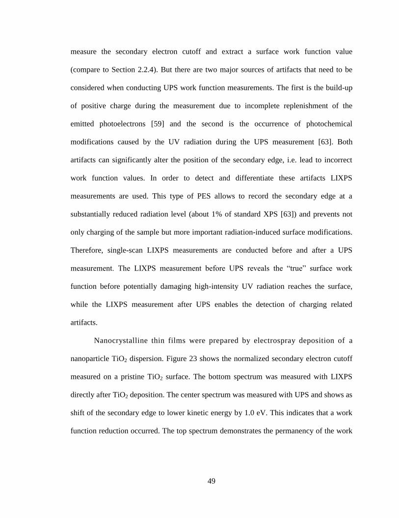
49
measure the secondary electron cutoff and extract a surface work function value
(compare to Section 2.2.4). But there are two major sources of artifacts that need to be
considered when conducting UPS work function measurements. The first is the build-up
of positive charge during the measurement due to incomplete replenishment of the
emitted photoelectrons [59] and the second is the occurrence of photochemical
modifications caused by the UV radiation during the UPS measurement [63]. Both
artifacts can significantly alter the position of the secondary edge, i.e. lead to incorrect
work function values. In order to detect and differentiate these artifacts LIXPS
measurements are used. This type of PES allows to record the secondary edge at a
substantially reduced radiation level (about 1% of standard XPS [63]) and prevents not
only charging of the sample but more important radiation-induced surface modifications.
Therefore, single-scan LIXPS measurements are conducted before and after a UPS
measurement. The LIXPS measurement before UPS reveals the “true” surface work
function before potentially damaging high-intensity UV radiation reaches the surface,
while the LIXPS measurement after UPS enables the detection of charging related
artifacts.
Nanocrystalline thin films were prepared by electrospray deposition of a
nanoparticle TiO2 dispersion. Figure 23 shows the normalized secondary electron cutoff
measured on a pristine TiO2 surface. The bottom spectrum was measured with LIXPS
directly after TiO2 deposition. The center spectrum was measured with UPS and shows as
shift of the secondary edge to lower kinetic energy by 1.0 eV. This indicates that a work
function reduction occurred. The top spectrum demonstrates the permanency of the work
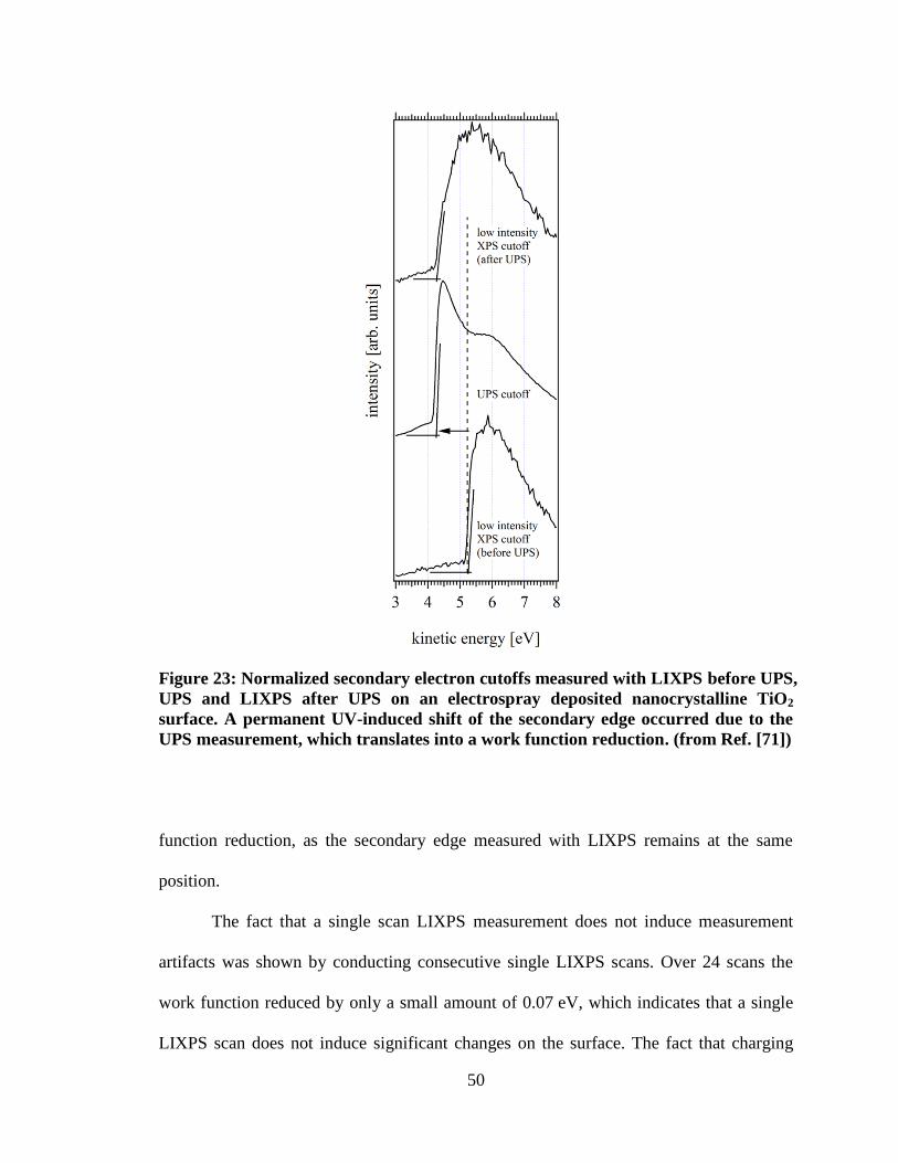
50
Figure 23: Normalized secondary electron cutoffs measured with LIXPS before UPS,
UPS and LIXPS after UPS on an electrospray deposited nanocrystalline TiO2
surface. A permanent UV-induced shift of the secondary edge occurred due to the
UPS measurement, which translates into a work function reduction. (from Ref. [71])
function reduction, as the secondary edge measured with LIXPS remains at the same
position.
The fact that a single scan LIXPS measurement does not induce measurement
artifacts was shown by conducting consecutive single LIXPS scans. Over 24 scans the
work function reduced by only a small amount of 0.07 eV, which indicates that a single
LIXPS scan does not induce significant changes on the surface. The fact that charging
51
Figure 24: Secondary edge spectra showing the absence of the work function
reducing effect on an annealed sample and recurrence of the effect after exposure of
the annealed surface to ambient air. (from Ref. [71])
can be excluded as a reason for the work function reduction was confirmed by a time
resolved series of LIXPS scans, which yielded an unchanged work function. A
nanocrystalline TiO2 thin film was annealed in order to create a more conductive film. A
side effect of the annealing process was the removal of adsorbates, such as residual
contamination (mainly water) of the electrospray process. Work function measurements
on the annealed surface revealed that no sample charging occurred nor a work function
reduction occurred. The re-exposure of the surface to ambient air resulted in a recurrence
52
of the work function reducing effect. Secondary edge spectra measured on the two
surfaces are shown in Figure 24. The result of these two experiments demonstrates that
ambient contamination must be present on the surface for the work function reducing
effect to occur. Furthermore, the results show that a work function reduction occurs even
on the more conductive annealed surface, which further supports that charging artifacts
are not the reason for the shift of the secondary edge upon UV illumination during the
UPS measurement. The question whether the UV-altered work function values would
revert back to the high work function over time was addressed in an additional
experiment, where single scan LIXPS measurements were conducted at certain time steps
after the UPS measurement. It was found that work functions remained permanently
reduced and did not revert back to the work function measured before UV exposure.
Based on the results obtain in this study, and in combination with supporting
literature a hypothesis about the work function reducing mechanism was developed.
Results obtained in a temperature programmed desorption study (TPD) revealed that
annealing a TiO2 (110) substrate to 700 K completely removes adsorbed water [72]. In
light of this report, it was concluded that residual contamination (originating from the
electrospray process) on the surface of the nanocrystalline TiO2 thin film was removed by
annealing. Since the UV-induced work function reduction recurred after sample exposure
to ambient humidity, it is reasonable to conclude that a requisite for the UV-induced
work function reduction to occur is the presence of a water layer on the surface. The
stability of up to one monolayer of molecularly adsorbed water on the surface in vacuum
was shown by Brinkley et al. [73]. A report by Henrich et al. [74] showed that a gradual
reduction of the work function (0.5-0.6 eV) of an ion-bombarded TiO2 (110) single
53
crystal surface occurred when water vapor was leaked into the vacuum chamber. The
authors in Ref. [74] concluded that water molecules dissociatively chemisorb at oxygen
vacancies, which results in the hydroxylation of the surface. Due to the excess of positive
charge on the outside of the surface caused by the oriented hydroxyl groups the work
function is reduced. In support of this hypothesis are reports about photo-induced
formation of oxygen vacancies [75, 76], which are also known to be reactive sites for
dissociative water splitting [77]. Other groups [78, 79] report the evolution of finite
amounts of hydrogen upon continuous UV illumination and explained this by the
passivation of defective surface sites with hydroxyl groups as well.
In consideration of the discussed reports it was concluded that the UV exposure
caused by the UPS measurement results in an instantaneous hydroxylation process on the
surface of TiO2 if there is molecularly adsorbed water present. The thereby induced work
function reduction is caused by the formation of a surface dipole through oriented
hydroxyl groups. The fact that this phenomenon was also observed on environmentally
contaminated ITO surfaces [59] justifies the investigation of the
ITO/nanocrystalline TiO2 interface with regard to the effects of the UV-induced work
function reduction on the interface electronic structure. Results of this investigation are
discussed in the following section.
3.2 Electronic structure of ITO/nanocrystalline TiO2 interfaces
Helped by manufacturing procedure under ambient conditions, dye-sensitized
solar cells are inexpensive alternatives to conventional silicon based photovoltaic cells
54
[80]. Transparent conductive oxide covered glass electrodes are cleaned under ambient
conditions and TiO2 paste is applied by coating techniques, such as doctor blading or
screen printing. These techniques inevitably introduce contamination to the hetero-
junction structure of the device. The reported sensitivity of ambient contaminated ITO
and TiO2 surfaces to UV radiation suggests that the electronic structure of the interfaces
might be affected by the UV illumination in presence of contamination. The conducted
study aimed at the investigation of charge injection barriers at the ITO/nanocrystalline
TiO2 interface before and after exposure to UV radiation with regard to the long-term
stability of DSSC devices. Since the oxide/oxide interface in DSSCs is usually subject to
annealing in order to produce conductive pathways, the annealed interface was
characterized as well.
The sensitivity of metal oxides to UV and x-ray radiation complicates the
determination of the interface electronic structure, since ITO substrate and overgrowing
TiO2 are both affected by UV-induced surface modifications. The extraction of the
electronic structure from a photoemission spectrum and the influence of UV radiation are
shown in Figure 25. The illustration shows a hypothetic overgrowth of semiconductor 2
(SC2) on top of a semiconductor 1 (SC1) substrate without the presence of band bending.
The binding energy reference point corresponds to the position of the Fermi level (EF).
The vacuum level position (Evac) is determined from the secondary electron cutoff which
can be translated into the work function (Φ) of the surface. LIXPS allows the extraction
of the true work function without the presence of charging or radiation induced surface
modifications. The transition from step (a) to (b) shows the formation of the UV-induced
surface dipole, as discussed above. The photochemically induced surface dipole is
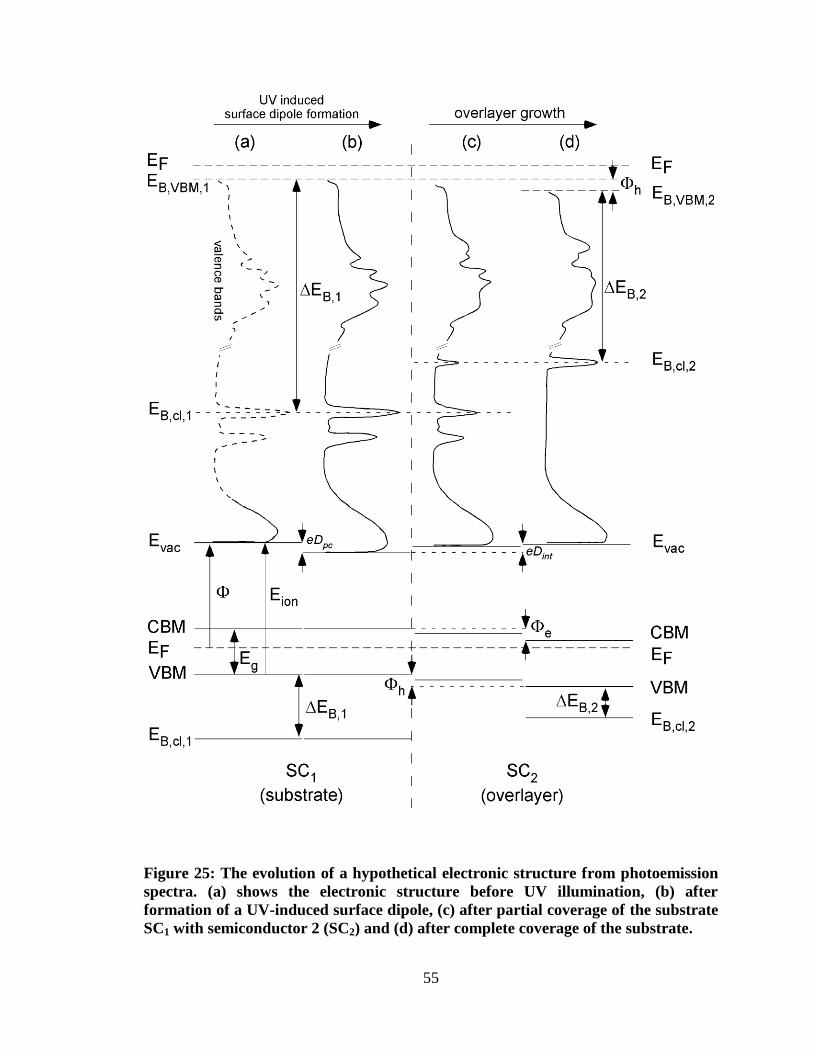
55
Figure 25: The evolution of a hypothetical electronic structure from photoemission
spectra. (a) shows the electronic structure before UV illumination, (b) after
formation of a UV-induced surface dipole, (c) after partial coverage of the substrate
SC1 with semiconductor 2 (SC2) and (d) after complete coverage of the substrate.
56
labeled as eDpc. UPS measurements can be used to track the formation of an interface
dipole (eDint) and the determination of the VBM position as the emissions change from
substrate to overlayer ((b) to (d)). Since the binding energy difference (ΔEB) between a
core level (EB,cl) and the VBM (EB,VBM) is constant the VBM position can also be
indirectly determined from the core level positions (EB,VBM = EB,cl-ΔEB), which are
measured with XPS. This is useful in case of superposition of the VBM position of the
underlying material. Combining the work function (Φ) with the binding energy position
of the VBM the ionization potential (Eion) can be determined. Hole injection barriers (Φh)
can then be calculated as the difference between VBM position of the substrate (EB,VBM,1)
and VBM position of the overlying material (EB,VBM,2). By using respective optical band
gap values (Eg) the conduction band minimum (CBM) position as well as the height of
injection barriers for electrons (Φe) can be estimated.
In this study nanocrystalline TiO2 was electrospray deposited in multiple steps on
a conductive ITO covered glass substrate, which was prepared in non-vacuum
environment, i.e. covered by environmental contamination. Since both materials are
exposed to ambient contaminants the investigation of the interface electronic structure
relies on the above discussed LIXPS measurement method. In combination with a UPS
derived method to obtain the ionization energy of nanocrystalline TiO2 it was possible to
determine the electronic structure of the interface before and after UV illumination.
Details about the experimental procedure can be found in Appendix C. As shown in
Figure 26 the absence of band bending was observed throughout the interface formation.
Results showed that band offsets are similar whether the interface was irradiated or not.
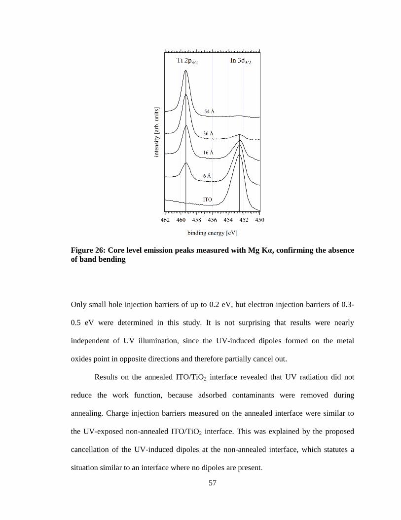
57
Figure 26: Core level emission peaks measured with Mg Kα, confirming the absence
of band bending
Only small hole injection barriers of up to 0.2 eV, but electron injection barriers of 0.3-
0.5 eV were determined in this study. It is not surprising that results were nearly
independent of UV illumination, since the UV-induced dipoles formed on the metal
oxides point in opposite directions and therefore partially cancel out.
Results on the annealed ITO/TiO2 interface revealed that UV radiation did not
reduce the work function, because adsorbed contaminants were removed during
annealing. Charge injection barriers measured on the annealed interface were similar to
the UV-exposed non-annealed ITO/TiO2 interface. This was explained by the proposed
cancellation of the UV-induced dipoles at the non-annealed interface, which statutes a
situation similar to an interface where no dipoles are present.
58
The conclusion of this investigation was that the ITO/TiO2 interface is fairly
robust with regard to preparation, and that annealing does not introduce a significant
change. It was also observed that UV exposure of the interface in presence of aqueous
contaminants resulted in an increase in electron injection barrier. Based on the outcome
of reported UV related long term stability studies, it was hypothesized that UV-induced
electronic structure alteration may contribute to the degradation of DSSCs.
59
CHAPTER 4: INVESTIGATION OF WORK FUNCTION CHANGES ON
NANOCRYSTALLINE ZINC OXIDE SURFACES
This chapter summarizes work function measurements on nanocrystalline ZnO
surfaces. A photo-induced work function reduction was found when water is present on
the surface. The work has been compiled in a manuscript and submitted to the Journal of
Applied Physics, where it is currently under review.
4.1 Introduction
Metal oxides are proving to possess advantageous electronic properties in an array
of optoelectronic applications, such as flat panel displays or photovoltaics [28]. One of
the metal oxides currently receiving significant attention is ZnO. The use of doped ZnO
in photovoltaics is being investigated as a potential low cost alternative for ITO as a
transparent conductive oxide (TCO) front contact [81, 82]. ZnO nanoparticles are
showing promise in hybrid organic solar cells where efficiencies of over 2% were
reported by blending PCBM into a P3HT/ZnO based device [83]. The electronic structure
of the interfaces between ZnO and other component materials in such devices is strongly
determined by the ZnO work function, which can be measured by UPS [84]. The work
function of a material is a key material property that determines the electronic structure of
60
contacts and hence crucially influences operational parameters such as open circuit
voltage and charge injection barriers.
UPS is considered the method of choice for work function measurements since it
yields absolute values. However, investigating metal oxide surfaces with photoemission
spectroscopy techniques has proven to be challenging due to artifacts such as sample
charging and photochemically induced surface modifications [59, 71]. The focus here is
whether ligand capped ZnO nanocrystals are also prone to this artifact, and, if so to
quantify its magnitude. Previously published results [59, 63, 71, 85, 86] on ITO, single
and nanocrystalline TiO2 surfaces, and single crystalline ZnO showed that the ionizing
radiation exposure during UPS and XPS measurements causes surface hydroxylation,
which results in an immediate work function reduction during the actual measurement
process. As a complicating side effect superimposed charging phenomena are also
usually encountered due to the high intensity UV photon flux photoionizing the typically
weakly conductive metal oxide samples.
In this study, LIXPS measurements were used to accurately determine the work
function of nanocrystalline ZnO surfaces, and to determine the magnitude of the UV-
induced artifacts. The results show that a work function reduction of 0.3-0.35 eV was
caused by UV exposure during UPS measurements, similar to what was previously
observed on ITO and TiO2 surfaces (~0.5 eV). A second experiment where a nano-
crystalline ZnO surface was annealed in vacuum to remove surface contamination
confirmed the hypothesis that surface hydroxylation by photo-induced H2O dissociation
is most likely responsible for the work function reduction.
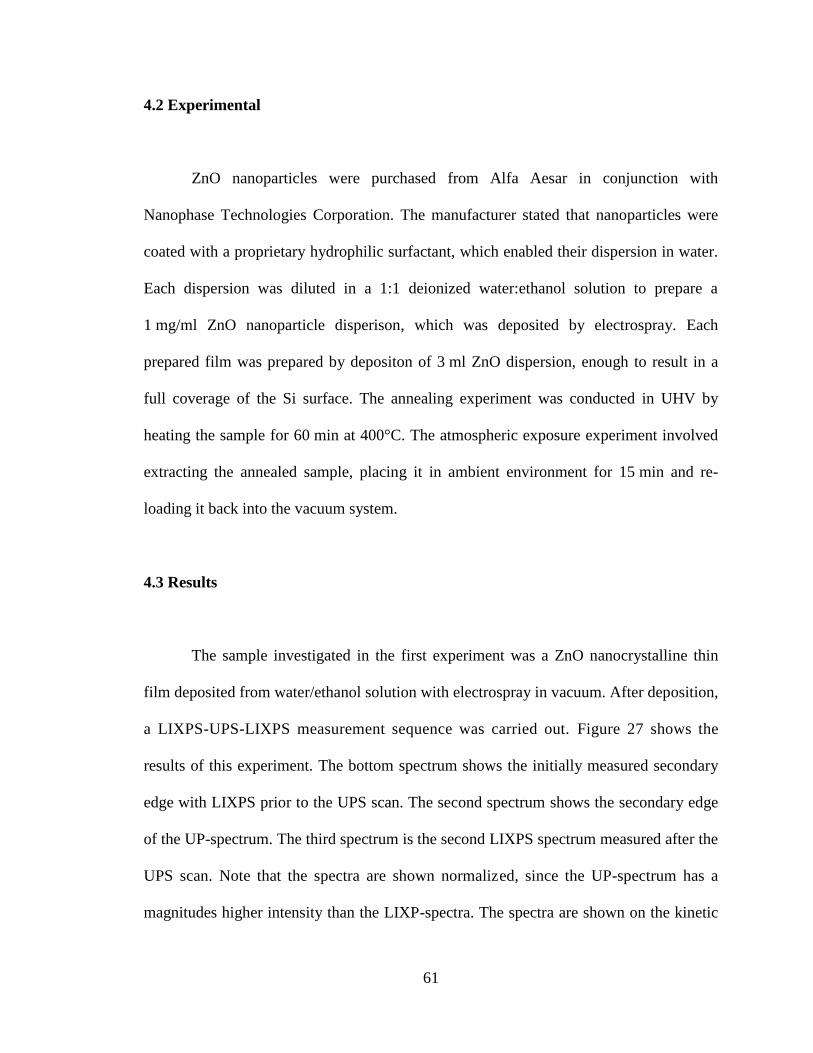
61
4.2 Experimental
ZnO nanoparticles were purchased from Alfa Aesar in conjunction with
Nanophase Technologies Corporation. The manufacturer stated that nanoparticles were
coated with a proprietary hydrophilic surfactant, which enabled their dispersion in water.
Each dispersion was diluted in a 1:1 deionized water:ethanol solution to prepare a
1 mg/ml ZnO nanoparticle disperison, which was deposited by electrospray. Each
prepared film was prepared by depositon of 3 ml ZnO dispersion, enough to result in a
full coverage of the Si surface. The annealing experiment was conducted in UHV by
heating the sample for 60 min at 400°C. The atmospheric exposure experiment involved
extracting the annealed sample, placing it in ambient environment for 15 min and re-
loading it back into the vacuum system.
4.3 Results
The sample investigated in the first experiment was a ZnO nanocrystalline thin
film deposited from water/ethanol solution with electrospray in vacuum. After deposition,
a LIXPS-UPS-LIXPS measurement sequence was carried out. Figure 27 shows the
results of this experiment. The bottom spectrum shows the initially measured secondary
edge with LIXPS prior to the UPS scan. The second spectrum shows the secondary edge
of the UP-spectrum. The third spectrum is the second LIXPS spectrum measured after the
UPS scan. Note that the spectra are shown normalized, since the UP-spectrum has a
magnitudes higher intensity than the LIXP-spectra. The spectra are shown on the kinetic
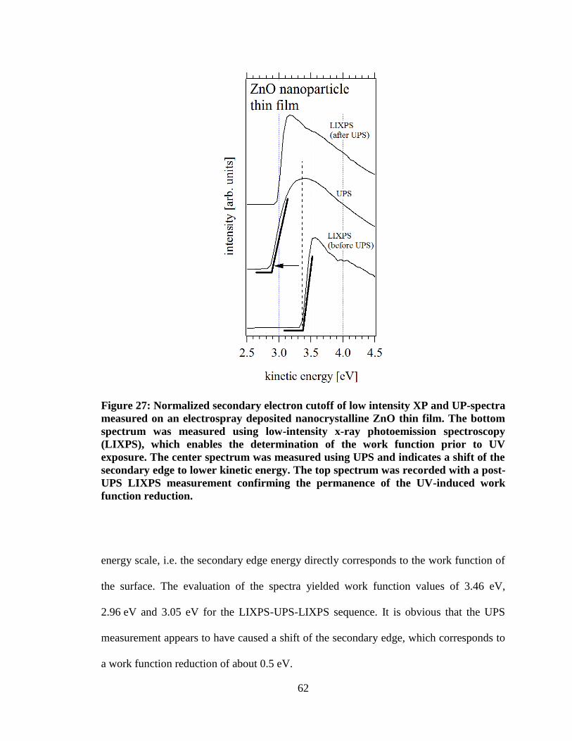
62
Figure 27: Normalized secondary electron cutoff of low intensity XP and UP-spectra
measured on an electrospray deposited nanocrystalline ZnO thin film. The bottom
spectrum was measured using low-intensity x-ray photoemission spectroscopy
(LIXPS), which enables the determination of the work function prior to UV
exposure. The center spectrum was measured using UPS and indicates a shift of the
secondary edge to lower kinetic energy. The top spectrum was recorded with a post-
UPS LIXPS measurement confirming the permanence of the UV-induced work
function reduction.
energy scale, i.e. the secondary edge energy directly corresponds to the work function of
the surface. The evaluation of the spectra yielded work function values of 3.46 eV,
2.96 eV and 3.05 eV for the LIXPS-UPS-LIXPS sequence. It is obvious that the UPS
measurement appears to have caused a shift of the secondary edge, which corresponds to
a work function reduction of about 0.5 eV.
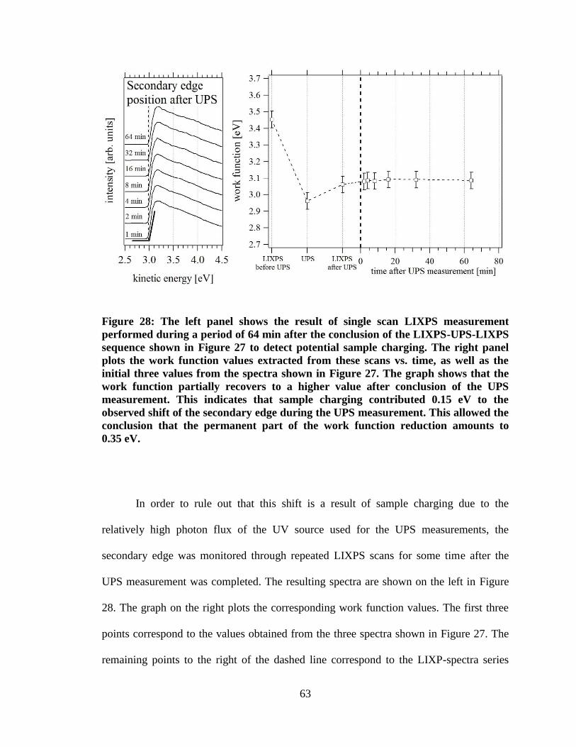
63
Figure 28: The left panel shows the result of single scan LIXPS measurement
performed during a period of 64 min after the conclusion of the LIXPS-UPS-LIXPS
sequence shown in Figure 27 to detect potential sample charging. The right panel
plots the work function values extracted from these scans vs. time, as well as the
initial three values from the spectra shown in Figure 27. The graph shows that the
work function partially recovers to a higher value after conclusion of the UPS
measurement. This indicates that sample charging contributed 0.15 eV to the
observed shift of the secondary edge during the UPS measurement. This allowed the
conclusion that the permanent part of the work function reduction amounts to
0.35 eV.
In order to rule out that this shift is a result of sample charging due to the
relatively high photon flux of the UV source used for the UPS measurements, the
secondary edge was monitored through repeated LIXPS scans for some time after the
UPS measurement was completed. The resulting spectra are shown on the left in Figure
28. The graph on the right plots the corresponding work function values. The first three
points correspond to the values obtained from the three spectra shown in Figure 27. The
remaining points to the right of the dashed line correspond to the LIXP-spectra series
64
shown on the left. The graph shows clearly that the UPS measurement lowers the work
function permanently, but also that there is a significant contribution of sample charging
to that value since the work function recovers by about 0.15 eV during the repeat LIXPS
measurements. Hence, it can be concluded that the balance of the UPS related work
function change, 0.35 eV, is permanent and a result of the hydroxylation of the surface.
The second experiment aimed to investigate the influence of the presence of
residual water and ethanol from the electrospray deposition process and the organic
ligand coating of the ZnO nanocrystals on the observed work function reduction. Hence,
an electrospray deposited ZnO thin film sample was annealed at 400°C inside the vacuum
system after the electrospray deposition step to remove surface contaminants. After the
annealing step, the work function of the sample was determined again with a LIXPS-
UPS-LIXPS sequence. The result of this measurement is shown in the bottom graph of
Figure 29. The derived work function values are 4.22 eV, 4.08 eV and 4.13 eV.
Considering the measurement resolution of ±0.1 eV the results show that the work
function of the annealed surface was not significantly affected by the UV exposure
during the UPS measurement. From this experiment it can be concluded that the surface
contamination is indeed crucial to producing the artifact.
To further strengthen this conclusion a third experiment was performed where the
annealed surface was exposed to the environment to re-establish a water film on the
surface. After re-insertion of the sample into the vacuum system the surface was yet
again investigated with a LIXPS-UPS-LIXPS sequence. The resulting secondary edge
spectra are shown in the top graph in Figure 29. The corresponding work function values
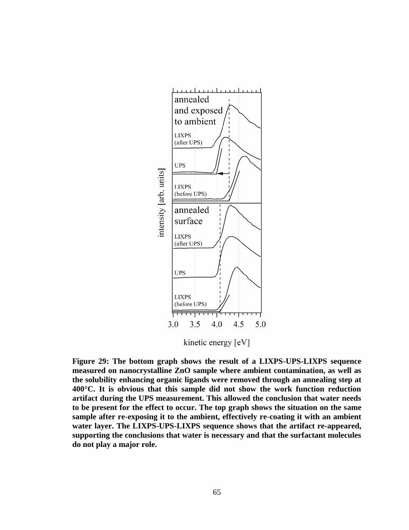
65
Figure 29: The bottom graph shows the result of a LIXPS-UPS-LIXPS sequence
measured on nanocrystalline ZnO sample where ambient contamination, as well as
the solubility enhancing organic ligands were removed through an annealing step at
400°C. It is obvious that this sample did not show the work function reduction
artifact during the UPS measurement. This allowed the conclusion that water needs
to be present for the effect to occur. The top graph shows the situation on the same
sample after re-exposing it to the ambient, effectively re-coating it with an ambient
water layer. The LIXPS-UPS-LIXPS sequence shows that the artifact re-appeared,
supporting the conclusions that water is necessary and that the surfactant molecules
do not play a major role.
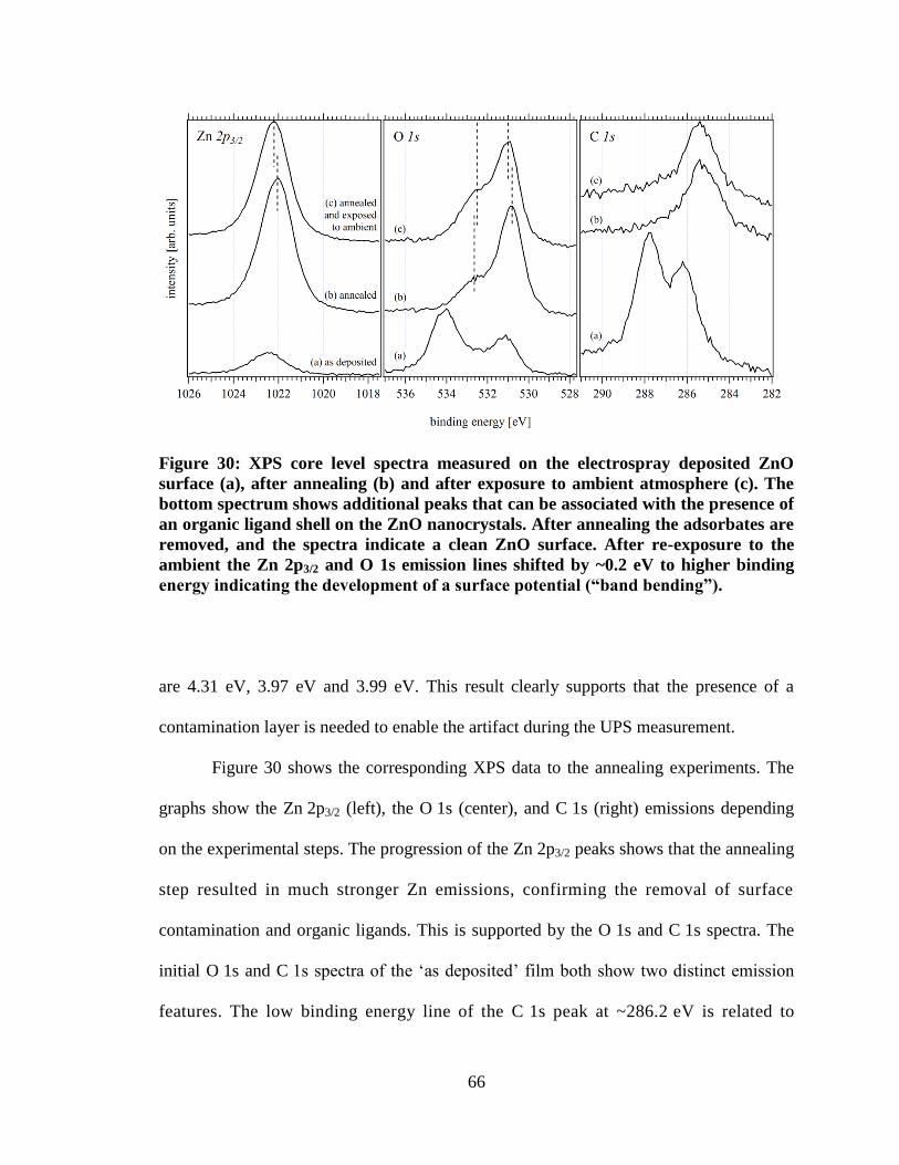
66
Figure 30: XPS core level spectra measured on the electrospray deposited ZnO
surface (a), after annealing (b) and after exposure to ambient atmosphere (c). The
bottom spectrum shows additional peaks that can be associated with the presence of
an organic ligand shell on the ZnO nanocrystals. After annealing the adsorbates are
removed, and the spectra indicate a clean ZnO surface. After re-exposure to the
ambient the Zn 2p3/2 and O 1s emission lines shifted by ~0.2 eV to higher binding
energy indicating the development of a surface potential (“band bending”).
are 4.31 eV, 3.97 eV and 3.99 eV. This result clearly supports that the presence of a
contamination layer is needed to enable the artifact during the UPS measurement.
Figure 30 shows the corresponding XPS data to the annealing experiments. The
graphs show the Zn 2p3/2 (left), the O 1s (center), and C 1s (right) emissions depending
on the experimental steps. The progression of the Zn 2p3/2 peaks shows that the annealing
step resulted in much stronger Zn emissions, confirming the removal of surface
contamination and organic ligands. This is supported by the O 1s and C 1s spectra. The
initial O 1s and C 1s spectra of the „as deposited‟ film both show two distinct emission
features. The low binding energy line of the C 1s peak at ~286.2 eV is related to
67
contamination. The second peak at ~287.8 eV is characteristic for C-O bonds, and is most
likely related to the organic ligands on the surface of the ZnO particles. The O 1s
spectrum shows two distinct lines, as well as evidence of a weaker third emission feature
in-between the main feature related to adsorbed water and/or defect sites in the ZnO
lattice. The low binding energy line at ~531 eV originates from emissions from oxygen
bonded in the ZnO lattice, while the high binding energy feature is most likely related to
oxygen contained in the organic ligand. Unfortunately, Nanophase Technologies was
unwilling to divulge the nature of their ligands, i.e. a matching of peak intensities to
ligand stoichiometry is not possible. However, this interpretation is supported by the
results of the annealing experiment. After annealing the sample the C 1s and O 1s lines
assigned to the ligands were completely attenuated, suggesting that they are most likely
not related to the ZnO structure. The O 1s and C 1s spectra after the annealing step are
characteristic for ZnO surfaces with a significant defect density [87, 88], and some
residual contamination. There is only a slight change in the O 1s spectrum after the
annealed surface was exposed to the ambient and re-inserted into the vacuum chamber.
The main ZnO related peak shifted to higher binding energy by about 0.2 eV, which
indicates the development of band bending in the ZnO surface after exposure to the
ambient, while the secondary O 1s peak at about 532.5 eV shifted to lower binding
energy by about 0.1 eV, while slightly increasing in intensity. This is the result of a
superposition of adsorbed water related emissions to the spectrum of the annealed surface.
Figure 31 shows the matching UP-spectra sequence. The emission features of the
spectrum of the „as deposited‟ sample (bottom) are probably a combination between
emissions from the organic ligands as well as the present surface contamination. The
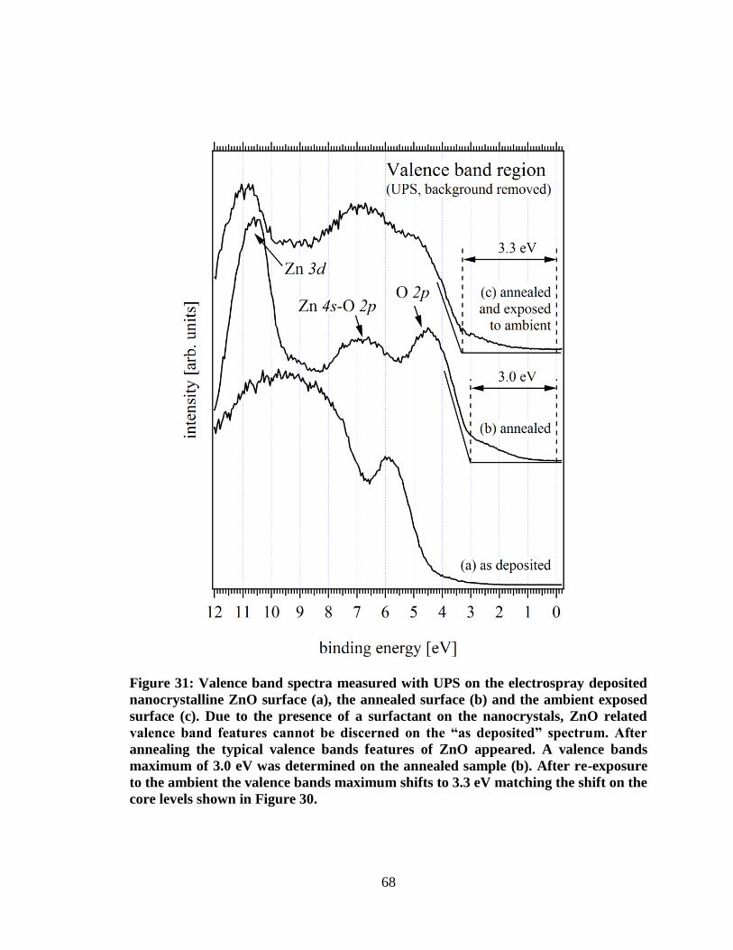
68
Figure 31: Valence band spectra measured with UPS on the electrospray deposited
nanocrystalline ZnO surface (a), the annealed surface (b) and the ambient exposed
surface (c). Due to the presence of a surfactant on the nanocrystals, ZnO related
valence band features cannot be discerned on the “as deposited” spectrum. After
annealing the typical valence bands features of ZnO appeared. A valence bands
maximum of 3.0 eV was determined on the annealed sample (b). After re-exposure
to the ambient the valence bands maximum shifts to 3.3 eV matching the shift on the
core levels shown in Figure 30.
69
distinct feature at ~5.8 eV is most likely related to the highest occupied molecular orbital
(HOMO) of the ligand molecules. The second spectrum in this graph is related to the
annealed surface and shows the typical valence bands spectra of the ZnO surface. The
three main features of these spectra can be assigned to Zn 3d (~10.5 eV), Zn 4s-O 2p
(~6.5-7.5 eV) and O 2p (4.5 eV) related states [89]. The spectrum on top is related to the
annealed sample after exposure to the ambient. The reintroduction of a contamination
layer reduced the emissions from the ZnO surface, and introduced additional emissions in
the range between 5 and 8 eV, which are related to adsorbed water and hydrocarbons.
4.4 Discussion
The shift between the initial LIXPS and UPS secondary edge spectra depicted in
Figure 27 clearly shows that nanocrystalline ZnO films exhibit the same work function
lowering artifact during UPS measurements as was shown previously for the cases of
ITO and single- and nanocrystalline TiO2 surfaces that were exposed to atmosphere
(i.e. which had an ambient contamination layer on their surface). It is likely that the
origin of the work function reduction caused by the UV light exposure during the UPS
measurement is also in the case of ZnO related to the photochemical chemisorption of
OH groups at “native” oxygen vacancy defects, as well as at additional defect sites
created by the UV exposure itself [43, 59, 71]. The data shown in Figure 28 shows that
sample charging only played a limited role in the observed shifts since the secondary
edge energy stabilized after a few minutes, indicating dissipation of positive charges that
resulted from the photoemission effect. The permanent component of the secondary edge
70
shift corresponds to a work function reduction of 0.35 eV caused by the UV light. This
value is slightly smaller than the previously measured values on ITO and TiO2 surfaces,
which showed work function reductions of about 0.5 eV or higher.
It is noteworthy that this effect occurred on a ZnO nanoparticle surface despite the
presence of solubility enhancing ligands introduced during the synthesis process of the
ZnO nanocrystals. The second experiment on an annealed sample clearly showed that the
ligands do not participate significantly in the work function lowering phenomenon. After
removal of most of the surface contamination as well as the ligands, the samples did not
show the work function effect anymore. This is shown in the bottom graph in Figure 29,
where the LIXPS-UPS-LIXPS sequence for such an annealed sample is shown. No
significant changes are apparent between the three spectra, which means that the work
function remained constant throughout the experiment. Charging is also absent in such
samples, presumably due to enhanced conductivity in absence of the insulating ligand
shells.
Exposure of annealed samples to the ambient restored the work function reduction
artifact. The corresponding LIXPS-UPS-LIXPS sequence is shown in the top graph of
Figure 29, where the UPS measurement again caused a shift to smaller work function.
This shows that the presence of contamination is a required ingredient in this effect. The
magnitude of the observed work function reduction of ~0.3 eV is very close to that found
on the initial „as deposited‟ sample (0.35 eV). This indicates that the presence of the
organic ligands is mostly irrelevant for the formation of the OH-attachment based surface
dipole. However, the absolute work function of the nanocrystalline surface is influenced
by the ligands. This is obvious from the almost 1 eV larger secondary edge energy of the
71
annealed sample that was exposed to the ambient compared to the „as deposited‟ sample.
This difference is clearly related to the formation of an interface dipole at the organic
ligand/ZnO crystal interface. This interface dipole is a result of the formation of the
chemical bond, as well as a potential dipole across the attached ligands themselves [90].
In this context the additional dipole potential created by the UV driven photo-
hydroxylation of the surface appears independently created and is superimposed to the
interface dipole at ligand-ZnO sites. This conclusion is supported by the fact that the UV
induced work function change has the same magnitude on both samples, with or without
organic ligands attached.
With regard to the absolute work function values that were measured, it is
interesting to compare with previously measured values. A recent investigation of co-
sputtered ZnO thin films performed by the author‟s group with LIXPS yielded a work
function of 4.3 eV for samples that were exposed to air prior to the measurement [87].
This value compares very well with the here presented measurement on the annealed and
subsequently exposed to the ambient sample. This is not surprising since the annealing
process results in fusing of the nanocrystals into larger units, not too different from a
polycrystalline film. These values are also comparable to what has been extracted from I-
V measurements on ZnO/Si hetero-junctions. These experiments yielded values between
4.45 eV and 4.50 eV [91]. The work function value found for the annealed surface
(4.1 eV) agrees well with a published value by Kim et al. [92] They measured a UPS
derived work function of 4.08 eV on an Ar+ ion sputtered / heat treated (700°C) ZnO
single crystal surface.
72
Closer inspection of the Zn 2p3/2 and O 1s core level lines shown in Figure 30
reveals a small 0.2 eV shift of the spectra to higher binding energy after the annealed
sample is exposed to the environment. A similar shift is obvious in the Zn 3d feature in
the UP-spectra shown in Figure 31. This uniform shift of spectral features related to
different atomic species indicates that the exposure to the ambient caused a surface
potential (“band bending”). It is not clear from the data whether this change already was
present before UV/x-ray exposure or not. This is due to the fact that the state of the
surface before the UPS or XPS measurement cannot be assessed as benchmark since an
XPS measurement would have been required to characterize the surface. However, this
would have already affected the artifact, hence, the “before radiation exposure” state of
the sample is not accessible. While LIXPS measurements do not expose the sample to
enough photon flux to affect the artifact, they only give access to the secondary edge.
Unfortunately, the secondary edge energy is affected both by work function changes as
well as band bending, and separation of the two effects is impossible without access to
core level spectra.
Using these data it is possible to determine the electronic structure of the sample
after the annealing process, and after the work function artifact occurs on the ambient-
exposed sample. From the UP-spectra the binding energy of the VBM can be determined.
This is shown graphically in Figure 31 where the low binding energy spectral cutoffs for
both UP-spectra are indicated by lines intersecting with the zero line. The line positions
account for 0.1 eV analyzer broadening of the spectrum. VBM binding energies of 3.0 eV
after annealing, and 3.3 eV after exposure to the ambient and subsequent UV exposure
were determined. This shift is in close agreement with the core level shifts observed in
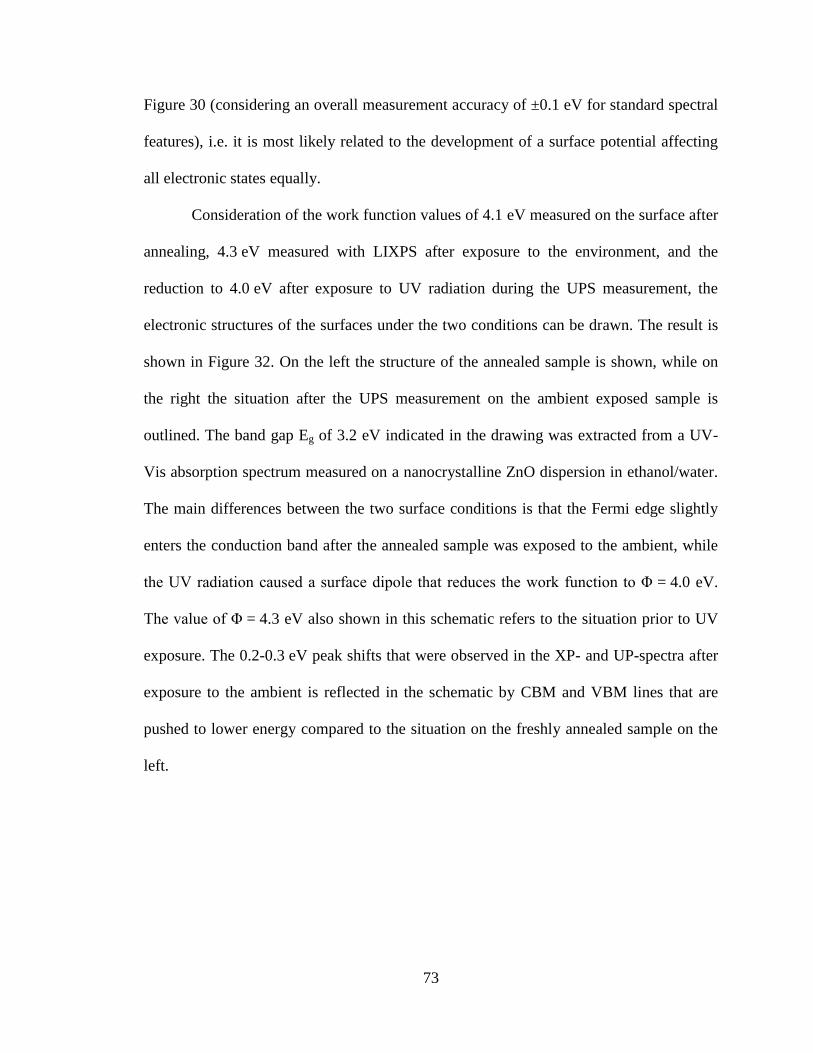
73
Figure 30 (considering an overall measurement accuracy of ±0.1 eV for standard spectral
features), i.e. it is most likely related to the development of a surface potential affecting
all electronic states equally.
Consideration of the work function values of 4.1 eV measured on the surface after
annealing, 4.3 eV measured with LIXPS after exposure to the environment, and the
reduction to 4.0 eV after exposure to UV radiation during the UPS measurement, the
electronic structures of the surfaces under the two conditions can be drawn. The result is
shown in Figure 32. On the left the structure of the annealed sample is shown, while on
the right the situation after the UPS measurement on the ambient exposed sample is
outlined. The band gap Eg of 3.2 eV indicated in the drawing was extracted from a UV-
Vis absorption spectrum measured on a nanocrystalline ZnO dispersion in ethanol/water.
The main differences between the two surface conditions is that the Fermi edge slightly
enters the conduction band after the annealed sample was exposed to the ambient, while
the UV radiation caused a surface dipole that reduces the work function to Φ = 4.0 eV.
The value of Φ = 4.3 eV also shown in this schematic refers to the situation prior to UV
exposure. The 0.2-0.3 eV peak shifts that were observed in the XP- and UP-spectra after
exposure to the ambient is reflected in the schematic by CBM and VBM lines that are
pushed to lower energy compared to the situation on the freshly annealed sample on the
left.
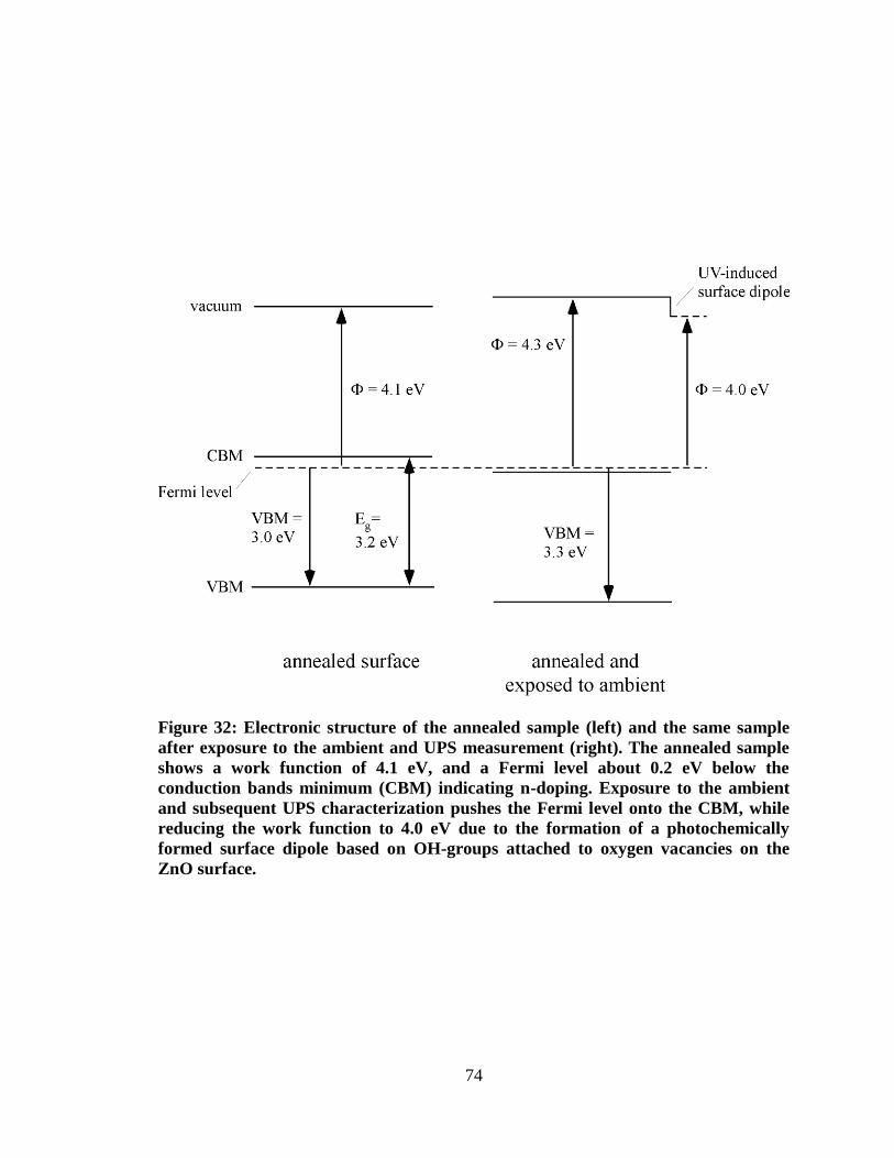
74
Figure 32: Electronic structure of the annealed sample (left) and the same sample
after exposure to the ambient and UPS measurement (right). The annealed sample
shows a work function of 4.1 eV, and a Fermi level about 0.2 eV below the
conduction bands minimum (CBM) indicating n-doping. Exposure to the ambient
and subsequent UPS characterization pushes the Fermi level onto the CBM, while
reducing the work function to 4.0 eV due to the formation of a photochemically
formed surface dipole based on OH-groups attached to oxygen vacancies on the
ZnO surface.
75
CHAPTER 5: ELECTRONIC STRUCTURE OF FUNCTIONALIZD CADMIUM
SELENIDE NANOPARTICLES
5.1 Introduction
The tunability of the band gap and the intrinsic electronic structure of inorganic
semiconducting nanocrystals through size modification makes cadmium selenide (CdSe)
[93, 94] a promising candidate for novel hybrid photovoltaic cells [6, 25, 95-98] or light-
emitting diodes (LEDs) [7, 99]. To date, hybrid structures used in photovoltaics are
usually made up of physical mixtures of inorganic nanocrystalline material and organic
conductive polymers. Unfortunately, the light conversion efficiency of such devices is
currently only about 3% [5]. A key limiting factor is the presence of organic insulating
capping molecules, such as tri-n-octylphosphine oxide (TOPO) at the surface of the
nanocrystals [100]. The particle synthesis requires the passivation in order to reduce the
number of dangling bonds and to stop the growth of nanoparticles at a specific particle
diameter. Furthermore, the capping of the nanocrystals prevents aggregation and
increases the solvent dispersivity. Ginger et al. [101] found that TOPO ligands have a
very low electron mobility compared to the mobility within the bulk CdSe, which
prevents the formation of a good interface for charge transfer [25]. Due to the different
bonding strengths it is possible to exchange the attached ligands to shorter capping
ligands, which reduces the inter-particle distance. Pyridine treatment has shown to
76
Figure 33: Schematic of a conductive polymer/CdSe nanocrystal composite. (a) The
coating of the CdSe nanocrystal with TOPO molecules constitutes a barrier for
charge separation. (b) an increase in charge separation efficiency can be expected
upon functionalization of the hybrid nanocrystals and direct linkage to the
conductive polymer phase.
increase the efficiency of such devices, as it replaces the insulating ligand with shorter
and more conductive pyridine molecules [6, 96, 97].
A promising approach to increase the charge separation efficiency of such
inorganic/organic hybrid materials is the preparation of a covalently-linked
organic/inorganic hybrid structure. Figure 33 shows a schematic of this theoretical
approach. Due to the absence of insulating capping molecules and the electronic coupling
to the conductive polymer charge separation efficiency can be increased. Based on this
concept, a synthesis route involving the modification of functional groups of the polymer
with amine or thiol groups was reportedly pursued [102-105]. The goal is to enable the
77
miscibility of the nanoparticles in the polymer, but so far only non-covalent interactions
have been reported. Another route is the direct synthesis of nanocrystals in the polymer
phase. As reported by Dayal et al. [106], the sulfur functionality in P3HT can act as an
anchor group for nanocrystal nucleation. Yet, the synthesis of covalently linked and
electronically coupled materials remains challenging and requires a development of
sophisticated synthesis strategies. A novel approach is addition of conductive polymers
(e.g. P3HT) with modified end-functionalities, which enable a covalent interaction of the
polymer and the nanocrystal.
Photoemission spectroscopic investigations can be helpful in order to understand
bonding mechanisms between organic and inorganic components, and to measure the
magnitude of the charge injection barriers at their interface. Knowledge of the electronic
structure of these materials can contribute in the search for molecule-semiconductor pairs
with an appropriate absorption spectrum, while also having an electronic structure
optimized for efficient exciton separation. In the here presented model study CdSe
nanocrystals were functionalized with a small organic molecule containing a hetero-atom
that enables the monitoring of its chemical environment before and after reaction with the
nanocrystal. XPS studies were performed to determine core-level binding energies and
UPS studies provided information about the VBM and HOMO energies. The secondary
electron cutoff of the UP-spectra yields the energy of the vacuum level and enables the
determination of work function Φ and ionization potential Eion. The chemical reaction
between an inorganic nanoparticle and organic ligand forms an organics-functionalized
hybrid nanoparticle. The hybrid-internal orbital line-up at the interface of the two
components is challenging, because VB emissions of the nanocrystal and HOMO
78
emissions of the organic ligand overlap and cannot be separated. In order to circumvent
this problem XPS derived core-level emission peaks can be used for determination of the
electronic structure, because core-level to VBM (HOMO) binding energy differences are
material constants. Figure 34 illustrates the theoretical approach for such measurements.
At first, the isolated components (CdSe nanocrystals and organic ligand material) are
characterized. This allows the determination of the core-level to highest occupied energy
level (HOMO or VBM, respectively) binding energy difference for each of the materials
independently. This can be used for the characterization of the hybrid material since
despite the superimposed HOMO emissions core-levels related to the inorganic
nanocrystal (ΔEB,CL1) and core-levels related to the organic ligand material (ΔEB,CL2) can
still be measured. Comparison of the relative binding energies of the core level emissions
in the hybrid molecule and the corresponding binding energies of the individual
components allows the direct quantification of the dipole potential between the inorganic
and organic component. The determined core-level to HOMO (VBM) binding energy
difference can then be used to calculate the respective HOMO energy for the ligand and
the VBM for the nanocrystal. The difference between these two values represents the
injection barrier between the nanocrystal and the organic ligand. Using the HOMO-
LUMO gaps determined by optical absorption spectroscopy, the electron injection
barriers can be estimated for the hybrid.
In this study, such XPS and UPS measurements were used to determine molecule-
internal charge injection barriers of ArSe-functionalized CdSe nanoparticles. It was found
that the Se 3d orbital of the arylselenophosphate ligand (ArSeP) shifted to higher binding
energy upon reaction of the organic ligand with the CdSe nanocrystal. In combination
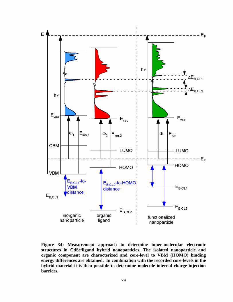
79
Figure 34: Measurement approach to determine inner-molecular electronic
structures in CdSe/ligand hybrid nanoparticles. The isolated nanoparticle and
organic component are characterized and core-level to VBM (HOMO) binding
energy differences are obtained. In combination with the recorded core-levels in the
hybrid material it is then possible to determine molecule internal charge injection
barriers.
80
with a shift to lower binding energy of the Cd 3d orbital, a hole injection barrier of 0.4 eV
was found. The ligand-nanoparticle interaction can be explained by classical
complexation chemistry, where the Se functionality of the ligand coordinates to the Cd
metal ions on the CdSe surface. It should be pointed out that the investigated hybrid
structure constitutes a model system that has at this point no direct applications but rather
serves the development of a PES measurement protocol that will enable the access to the
molecular electronic structure of organic/inorganic hybrid materials.
5.2 Experimental
The investigation of the electronic structure of functionalized CdSe nanoparticles
requires the characterization of clean nanoparticle surfaces that are free of organic
capping molecules. However, in order to preserve the dispersivity of such particles in a
solvent the presence of capping molecules is necessary. As reported earlier by several
groups, post-synthesis pyridine treated CdSe nanoparticles contain pyridine capping
molecules that are unstable in ultra high vacuum and easily desorb from the CdSe
nanocrystal surface [107, 108], resulting in a useful CdSe surface. The CdSe nanocrystals
used in this study were provided by Elizabeth Strein from the University of Washington,
Seattle, WA. They were synthesized following the synthesis route described in Ref. [109].
After drying the crystals the ligands were then exchanged in air. With the aid of
sonication the nanocrystals were dispersed in pyridine and precipitated with excess
hexane for three times. The particles were then dried and dispersed in toluene at a
concentration of 1 mg/ml. A volume of 1.2 ml of dispersion was electrospray deposited
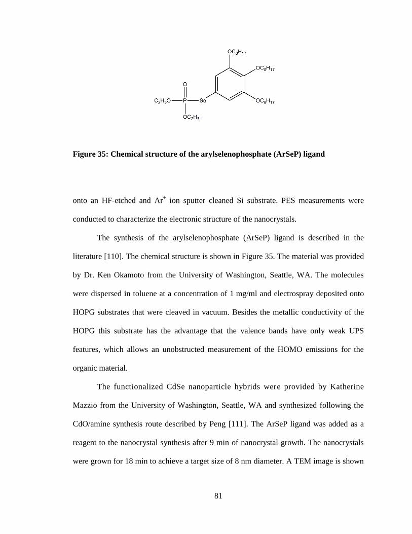
81
Figure 35: Chemical structure of the arylselenophosphate (ArSeP) ligand
onto an HF-etched and Ar+ ion sputter cleaned Si substrate. PES measurements were
conducted to characterize the electronic structure of the nanocrystals.
The synthesis of the arylselenophosphate (ArSeP) ligand is described in the
literature [110]. The chemical structure is shown in Figure 35. The material was provided
by Dr. Ken Okamoto from the University of Washington, Seattle, WA. The molecules
were dispersed in toluene at a concentration of 1 mg/ml and electrospray deposited onto
HOPG substrates that were cleaved in vacuum. Besides the metallic conductivity of the
HOPG this substrate has the advantage that the valence bands have only weak UPS
features, which allows an unobstructed measurement of the HOMO emissions for the
organic material.
The functionalized CdSe nanoparticle hybrids were provided by Katherine
Mazzio from the University of Washington, Seattle, WA and synthesized following the
CdO/amine synthesis route described by Peng [111]. The ArSeP ligand was added as a
reagent to the nanocrystal synthesis after 9 min of nanocrystal growth. The nanocrystals
were grown for 18 min to achieve a target size of 8 nm diameter. A TEM image is shown
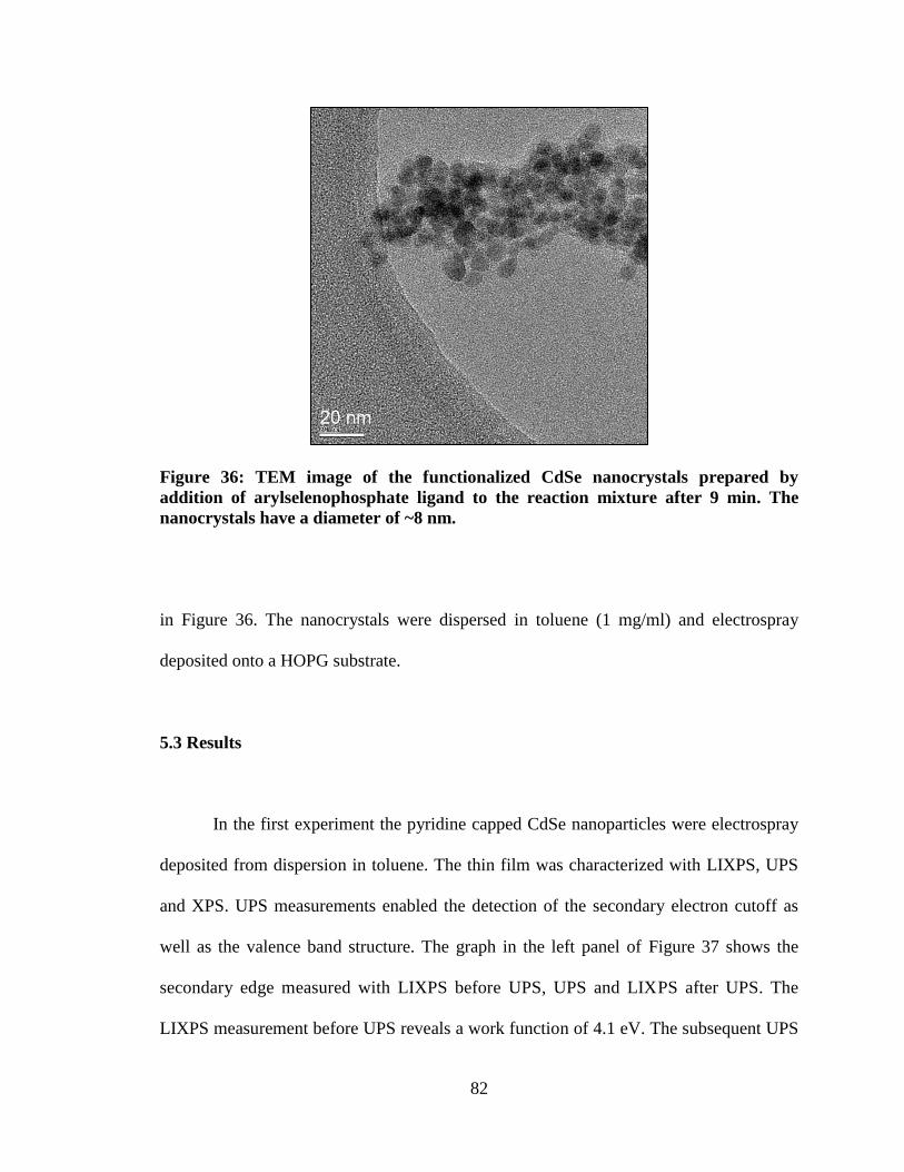
82
Figure 36: TEM image of the functionalized CdSe nanocrystals prepared by
addition of arylselenophosphate ligand to the reaction mixture after 9 min. The
nanocrystals have a diameter of ~8 nm.
in Figure 36. The nanocrystals were dispersed in toluene (1 mg/ml) and electrospray
deposited onto a HOPG substrate.
5.3 Results
In the first experiment the pyridine capped CdSe nanoparticles were electrospray
deposited from dispersion in toluene. The thin film was characterized with LIXPS, UPS
and XPS. UPS measurements enabled the detection of the secondary electron cutoff as
well as the valence band structure. The graph in the left panel of Figure 37 shows the
secondary edge measured with LIXPS before UPS, UPS and LIXPS after UPS. The
LIXPS measurement before UPS reveals a work function of 4.1 eV. The subsequent UPS
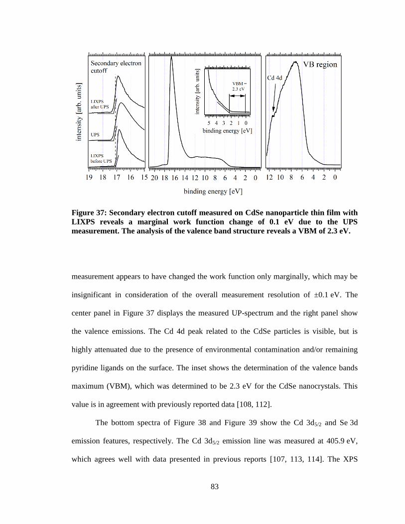
83
Figure 37: Secondary electron cutoff measured on CdSe nanoparticle thin film with
LIXPS reveals a marginal work function change of 0.1 eV due to the UPS
measurement. The analysis of the valence band structure reveals a VBM of 2.3 eV.
measurement appears to have changed the work function only marginally, which may be
insignificant in consideration of the overall measurement resolution of ±0.1 eV. The
center panel in Figure 37 displays the measured UP-spectrum and the right panel show
the valence emissions. The Cd 4d peak related to the CdSe particles is visible, but is
highly attenuated due to the presence of environmental contamination and/or remaining
pyridine ligands on the surface. The inset shows the determination of the valence bands
maximum (VBM), which was determined to be 2.3 eV for the CdSe nanocrystals. This
value is in agreement with previously reported data [108, 112].
The bottom spectra of Figure 38 and Figure 39 show the Cd 3d5/2 and Se 3d
emission features, respectively. The Cd 3d5/2 emission line was measured at 405.9 eV,
which agrees well with data presented in previous reports [107, 113, 114]. The XPS
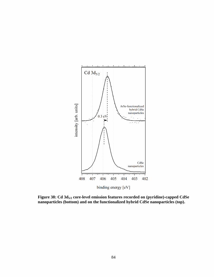
84
Figure 38: Cd 3d5/2 core-level emission features recorded on (pyridine)-capped CdSe
nanoparticles (bottom) and on the functionalized hybrid CdSe nanoparticles (top).
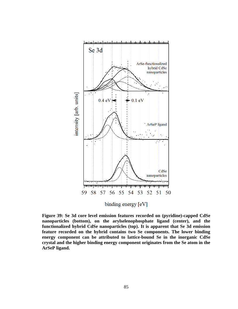
85
Figure 39: Se 3d core level emission features recorded on (pyridine)-capped CdSe
nanoparticles (bottom), on the arylselenophosphate ligand (center), and the
functionalized hybrid CdSe nanoparticles (top). It is apparent that Se 3d emission
feature recorded on the hybrid contains two Se components. The lower binding
energy component can be attributed to lattice-bound Se in the inorganic CdSe
crystal and the higher binding energy component originates from the Se atom in the
ArSeP ligand.
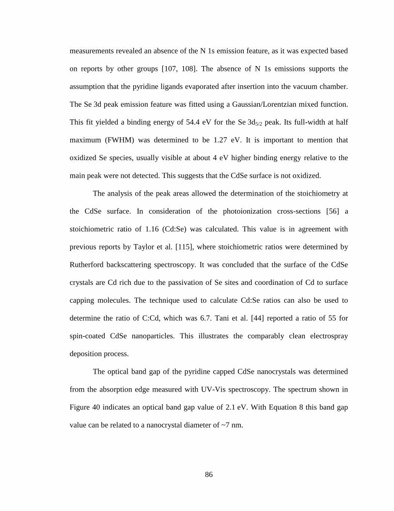
86
measurements revealed an absence of the N 1s emission feature, as it was expected based
on reports by other groups [107, 108]. The absence of N 1s emissions supports the
assumption that the pyridine ligands evaporated after insertion into the vacuum chamber.
The Se 3d peak emission feature was fitted using a Gaussian/Lorentzian mixed function.
This fit yielded a binding energy of 54.4 eV for the Se 3d5/2 peak. Its full-width at half
maximum (FWHM) was determined to be 1.27 eV. It is important to mention that
oxidized Se species, usually visible at about 4 eV higher binding energy relative to the
main peak were not detected. This suggests that the CdSe surface is not oxidized.
The analysis of the peak areas allowed the determination of the stoichiometry at
the CdSe surface. In consideration of the photoionization cross-sections [56] a
stoichiometric ratio of 1.16 (Cd:Se) was calculated. This value is in agreement with
previous reports by Taylor et al. [115], where stoichiometric ratios were determined by
Rutherford backscattering spectroscopy. It was concluded that the surface of the CdSe
crystals are Cd rich due to the passivation of Se sites and coordination of Cd to surface
capping molecules. The technique used to calculate Cd:Se ratios can also be used to
determine the ratio of C:Cd, which was 6.7. Tani et al. [44] reported a ratio of 55 for
spin-coated CdSe nanoparticles. This illustrates the comparably clean electrospray
deposition process.
The optical band gap of the pyridine capped CdSe nanocrystals was determined
from the absorption edge measured with UV-Vis spectroscopy. The spectrum shown in
Figure 40 indicates an optical band gap value of 2.1 eV. With Equation 8 this band gap
value can be related to a nanocrystal diameter of ~7 nm.
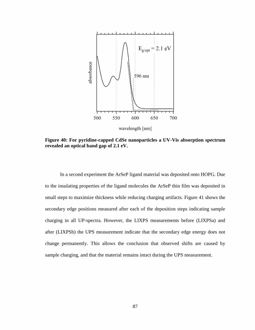
87
Figure 40: For pyridine-capped CdSe nanoparticles a UV-Vis absorption spectrum
revealed an optical band gap of 2.1 eV.
In a second experiment the ArSeP ligand material was deposited onto HOPG. Due
to the insulating properties of the ligand molecules the ArSeP thin film was deposited in
small steps to maximize thickness while reducing charging artifacts. Figure 41 shows the
secondary edge positions measured after each of the deposition steps indicating sample
charging in all UP-spectra. However, the LIXPS measurements before (LIXPSa) and
after (LIXPSb) the UPS measurement indicate that the secondary edge energy does not
change permanently. This allows the conclusion that observed shifts are caused by
sample charging, and that the material remains intact during the UPS measurement.
88
Figure 41: Secondary edge positions measured with LIXPS and UPS on
arylselenophosphate ligand indicates sample charging caused by high UV photon
flux. Beginning with the 0.12 ml deposition step charging is affecting the LIXPS
measurement after UPS.
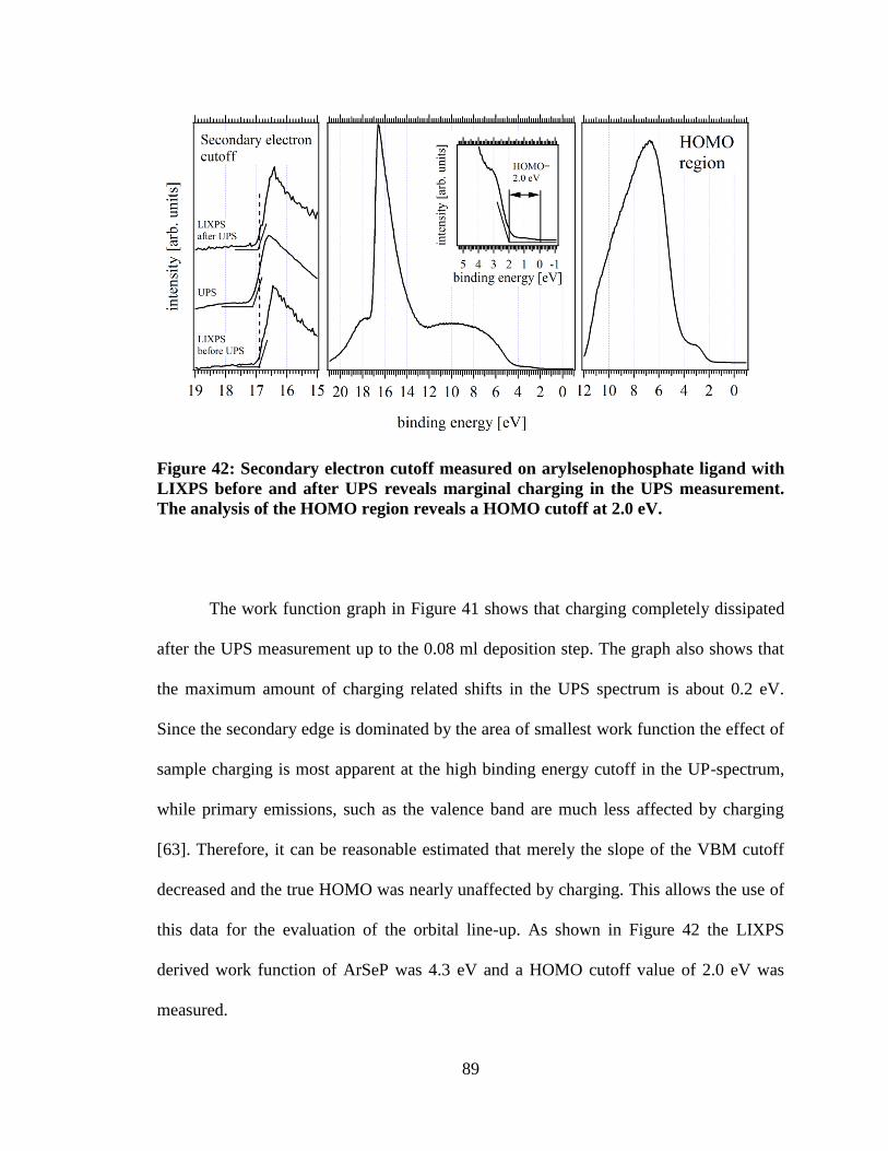
89
Figure 42: Secondary electron cutoff measured on arylselenophosphate ligand with
LIXPS before and after UPS reveals marginal charging in the UPS measurement.
The analysis of the HOMO region reveals a HOMO cutoff at 2.0 eV.
The work function graph in Figure 41 shows that charging completely dissipated
after the UPS measurement up to the 0.08 ml deposition step. The graph also shows that
the maximum amount of charging related shifts in the UPS spectrum is about 0.2 eV.
Since the secondary edge is dominated by the area of smallest work function the effect of
sample charging is most apparent at the high binding energy cutoff in the UP-spectrum,
while primary emissions, such as the valence band are much less affected by charging
[63]. Therefore, it can be reasonable estimated that merely the slope of the VBM cutoff
decreased and the true HOMO was nearly unaffected by charging. This allows the use of
this data for the evaluation of the orbital line-up. As shown in Figure 42 the LIXPS
derived work function of ArSeP was 4.3 eV and a HOMO cutoff value of 2.0 eV was
measured.
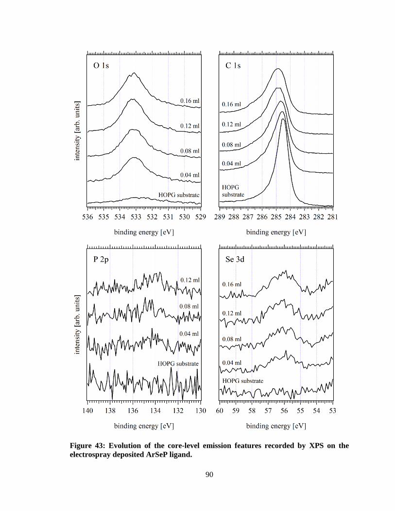
90
Figure 43: Evolution of the core-level emission features recorded by XPS on the
electrospray deposited ArSeP ligand.
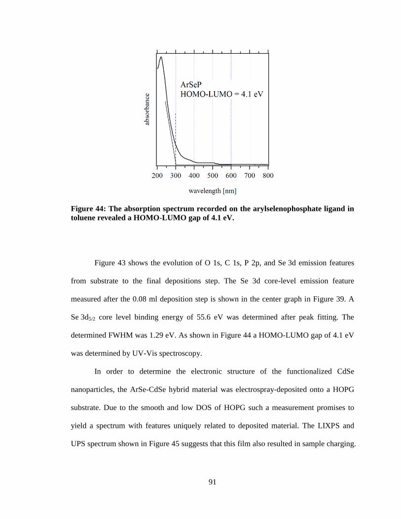
91
Figure 44: The absorption spectrum recorded on the arylselenophosphate ligand in
toluene revealed a HOMO-LUMO gap of 4.1 eV.
Figure 43 shows the evolution of O 1s, C 1s, P 2p, and Se 3d emission features
from substrate to the final depositions step. The Se 3d core-level emission feature
measured after the 0.08 ml deposition step is shown in the center graph in Figure 39. A
Se 3d5/2 core level binding energy of 55.6 eV was determined after peak fitting. The
determined FWHM was 1.29 eV. As shown in Figure 44 a HOMO-LUMO gap of 4.1 eV
was determined by UV-Vis spectroscopy.
In order to determine the electronic structure of the functionalized CdSe
nanoparticles, the ArSe-CdSe hybrid material was electrospray-deposited onto a HOPG
substrate. Due to the smooth and low DOS of HOPG such a measurement promises to
yield a spectrum with features uniquely related to deposited material. The LIXPS and
UPS spectrum shown in Figure 45 suggests that this film also resulted in sample charging.
92
Similar to the initial experiment the 0.08 ml deposition step data was selected for further
evaluation.
Figure 46 shows the corresponding evolution of the core-level emission features
measured on the ArSe-functionalized CdSe nanocrystals. For the 0.08 ml deposition step
a Cd 3d5/2 peak position with a maximum at 405.6 eV and a FWHM of 1.17 eV was
determined. For comparison the spectrum is shown in Figure 38. The top spectrum in
Figure 39 shows the measured Se 3d emission feature. Fitting of this line revealed two
components, which will be discussed with more detail in the following section. The
binding energies of the two components were determined to be 56.0 eV and 54.3 eV.
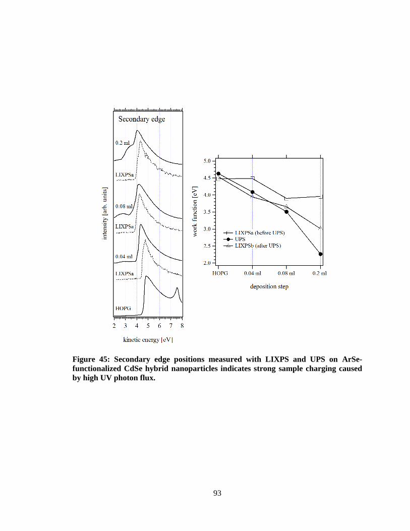
93
Figure 45: Secondary edge positions measured with LIXPS and UPS on ArSe-
functionalized CdSe hybrid nanoparticles indicates strong sample charging caused
by high UV photon flux.
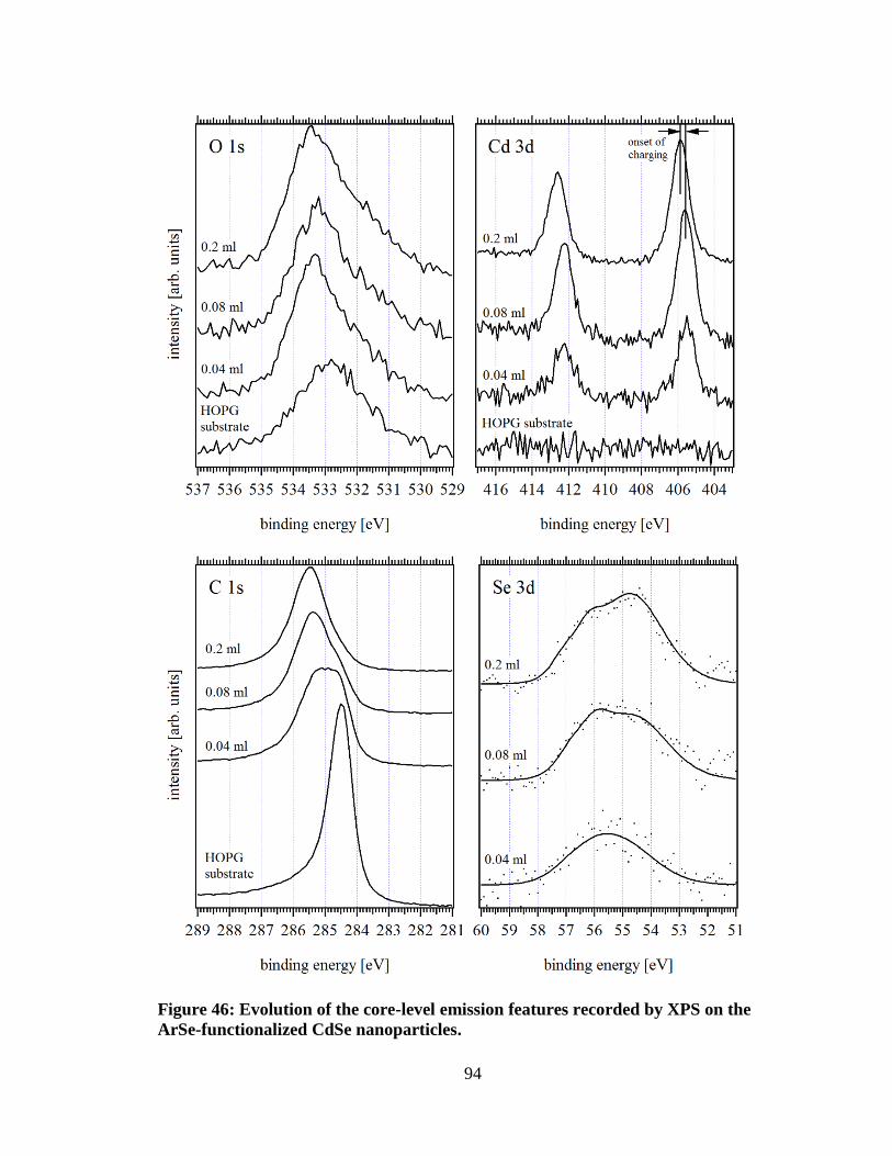
94
Figure 46: Evolution of the core-level emission features recorded by XPS on the
ArSe-functionalized CdSe nanoparticles.
95
5.4 Discussion
The presented experiments aimed at the development of a PES measurement
protocol to determine the orbital line-up at the organic/inorganic interface of a hybrid
molecule. XPS and UPS were used to determine the binding energy of hybrid
component-unique XPS relative to the highest occupied energy levels (VBM or HOMO).
As shown in Figure 38 the Cd 3d5/2 core level emission peak measured on the
ligand free CdSe nanocrystals was measured at 405.9 eV. After ligand attachment and
formation of the ArSe-functionalized CdSe nanocrystal hybrid this feature shifted 0.3 eV
to lower binding energy. Generally, binding energy shifts to lower values are explained
by a change in the chemical environment of core level electrons that receive negative
charge. Here, the accumulation of electron density at the Cd surface sites may be a result
of charge transfer from the Se functionality of the ligand to the Cd metal ions. With this
the binding energy of the electrons originating from the orbitals of the Se functionality
may have increased due to the loss of charges through complexation with Cd, as observed
by the 0.4 eV increase in binding energy of the Se 3d5/2 electrons. This hypothesis would
suggest a substantial interaction between the ligand and the nanocrystal.
Since such an interaction of the organic ligand with the nanocrystal is similar to
the basic mechanistic principles in classic coordination chemistry it is reasonable to
explain the interaction in context of the hard-soft-acid-base (HSAB) concept introduced
by Pearson [116]. Based on this principle metal ions interact with surrounding ligands,
while the metal ion acts as a Lewis acid or electron acceptor and the ligands act as Lewis
base, i.e. they donate electrons to the empty orbitals of the metal ion. Hard acids and
96
bases include species that have small sizes, high oxidation state, low electron cloud
polarizability and high electronegativity and through hard-hard interactions form mainly
ionic bonds. On the other hand, soft species possess opposite characteristics and generate
through soft-soft interactions covalent bonds. Therefore, the soft Se functionality of the
ArSeP ligand coordinates to the soft Lewis acidic Cd2+
ion on the surface of the
nanocrystal in an attempt to fill the Cd coordination sphere. This theory is supported by
reports by Liu et al. [114], where XPS data proves that ligands interact much stronger
with the Cd atom than the Se atoms on the surface of the nanocrystal. Puzder et al. [117,
118] calculated the binding energy of phosphine oxide to the CdSe nanoparticle facets
and found that the dominating binding interaction is between the oxygen atoms in the
ligands and the cadmium atoms on the surface, which furthermore agrees with the HSAB
concept.
As it can be seen in Figure 39, a second Se component can be found at lower
binding energy with a Se 3d5/2 emission maximum at 54.3 eV. This feature only
marginally differs from the Se 3d5/2 peak maximum measured on the ligand free CdSe
nanocrystals and the measured binding energy agrees well with the Se 3d5/2 peak position
observed in bulk CdSe [119]. Therefore, this feature can be assigned to the lattice Se in
the hybrid nanocrystal. In consideration of the low signal-to-noise ratio it was found that
the Se 3d5/2 electrons originating from the Se lattice are nearly unaffected by the
complexation of the CdSe nanocrystal with the ligand. This is not surprising as the ligand
interacts with the surface Cd sites. A similar system is the complexation of thiol
functional groups with Cd atoms on the CdSe surface to form Cd-S structures [120-122].
In these studies it was found that the Se 3d peak position is nearly constant for CdSe
97
nanoparticles capped with different ligands [114]. Figure 39 shows that the FWHM
changes from 1.27 eV for the pure CdSe nanocrystal to 2.71 eV for the functionalized
nanocrystal. This may be explained by the increasing structural disorder and interrupted
nanocrystal growth caused by the addition of the ArSeP ligand to the reaction mixture.
PES measurements with synchrotron radiation reported by Borchert et al. [113] revealed
that ligand-passivated Se surface atoms are found at higher binding energy, which might
contribute to the line broadening as well and reflect a possible interaction of ligand
moieties with lattice Se on the surface of the nanocrystal. But due to the preferred binding
of the Se atom in the ligand to the Cd in the crystal makes it impossible to resolve the
component corresponding to ligands bonded to Se.
Since the Se functionality of the ligand is expected to interact with the Cd sites
one would assume that only surface Cd sites are affected by the change in chemical
environment and that the Cd 3d5/2 peak emission would not only broaden, but also show
an indication of bulk and surface components. This was not observed. Other groups [113,
114] have reported a similar behavior and found that peak maxima shift for different
capping molecules while the shape of the Cd 3d emission feature does not change.
As mentioned in the Section 5.2, the ArSeP ligand was injected in the reaction
mixture towards the end of the synthesis of the CdSe nanocrystal with the aim to
terminate the nanocrystal surface to prevent further aggregation and particle growth.
Since the structure of the ArSeP ligand is similar to the phosphine selenide precursor
(TBP-Se) it is reasonable to hypothesize that the reaction pathway for ligand attachment
on the nanocrystal surface might also be analog to the mechanism of CdSe formation.
Recently, Liu et al. [123] investigated the reaction mechanism for a typical CdSe
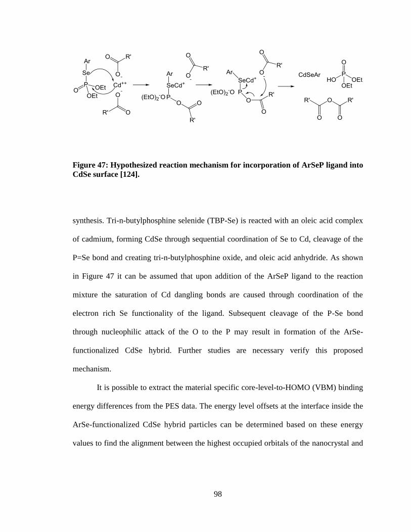
98
Figure 47: Hypothesized reaction mechanism for incorporation of ArSeP ligand into
CdSe surface [124].
synthesis. Tri-n-butylphosphine selenide (TBP-Se) is reacted with an oleic acid complex
of cadmium, forming CdSe through sequential coordination of Se to Cd, cleavage of the
P=Se bond and creating tri-n-butylphosphine oxide, and oleic acid anhydride. As shown
in Figure 47 it can be assumed that upon addition of the ArSeP ligand to the reaction
mixture the saturation of Cd dangling bonds are caused through coordination of the
electron rich Se functionality of the ligand. Subsequent cleavage of the P-Se bond
through nucleophilic attack of the O to the P may result in formation of the ArSe-
functionalized CdSe hybrid. Further studies are necessary verify this proposed
mechanism.
It is possible to extract the material specific core-level-to-HOMO (VBM) binding
energy differences from the PES data. The energy level offsets at the interface inside the
ArSe-functionalized CdSe hybrid particles can be determined based on these energy
values to find the alignment between the highest occupied orbitals of the nanocrystal and
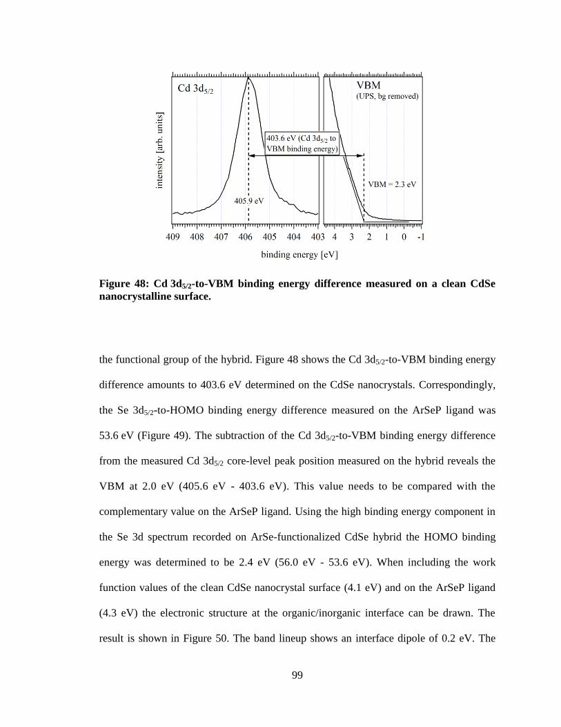
99
Figure 48: Cd 3d5/2-to-VBM binding energy difference measured on a clean CdSe
nanocrystalline surface.
the functional group of the hybrid. Figure 48 shows the Cd 3d5/2-to-VBM binding energy
difference amounts to 403.6 eV determined on the CdSe nanocrystals. Correspondingly,
the Se 3d5/2-to-HOMO binding energy difference measured on the ArSeP ligand was
53.6 eV (Figure 49). The subtraction of the Cd 3d5/2-to-VBM binding energy difference
from the measured Cd 3d5/2 core-level peak position measured on the hybrid reveals the
VBM at 2.0 eV (405.6 eV - 403.6 eV). This value needs to be compared with the
complementary value on the ArSeP ligand. Using the high binding energy component in
the Se 3d spectrum recorded on ArSe-functionalized CdSe hybrid the HOMO binding
energy was determined to be 2.4 eV (56.0 eV - 53.6 eV). When including the work
function values of the clean CdSe nanocrystal surface (4.1 eV) and on the ArSeP ligand
(4.3 eV) the electronic structure at the organic/inorganic interface can be drawn. The
result is shown in Figure 50. The band lineup shows an interface dipole of 0.2 eV. The
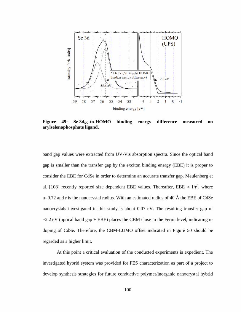
100
Figure 49: Se 3d5/2-to-HOMO binding energy difference measured on
arylselenophosphate ligand.
band gap values were extracted from UV-Vis absorption spectra. Since the optical band
gap is smaller than the transfer gap by the exciton binding energy (EBE) it is proper to
consider the EBE for CdSe in order to determine an accurate transfer gap. Meulenberg et
al. [108] recently reported size dependent EBE values. Thereafter, EBE ≈ 1/rn, where
n=0.72 and r is the nanocrystal radius. With an estimated radius of 40 Å the EBE of CdSe
nanocrystals investigated in this study is about 0.07 eV. The resulting transfer gap of
~2.2 eV (optical band gap + EBE) places the CBM close to the Fermi level, indicating n-
doping of CdSe. Therefore, the CBM-LUMO offset indicated in Figure 50 should be
regarded as a higher limit.
At this point a critical evaluation of the conducted experiments is expedient. The
investigated hybrid system was provided for PES characterization as part of a project to
develop synthesis strategies for future conductive polymer/inorganic nanocrystal hybrid
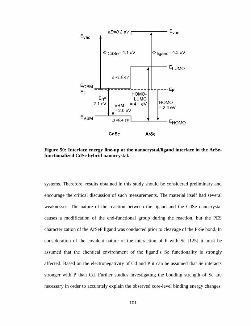
101
Figure 50: Interface energy line-up at the nanocrystal/ligand interface in the ArSe-
functionalized CdSe hybrid nanocrystal.
systems. Therefore, results obtained in this study should be considered preliminary and
encourage the critical discussion of such measurements. The material itself had several
weaknesses. The nature of the reaction between the ligand and the CdSe nanocrystal
causes a modification of the end-functional group during the reaction, but the PES
characterization of the ArSeP ligand was conducted prior to cleavage of the P-Se bond. In
consideration of the covalent nature of the interaction of P with Se [125] it must be
assumed that the chemical environment of the ligand‟s Se functionality is strongly
affected. Based on the electronegativity of Cd and P it can be assumed that Se interacts
stronger with P than Cd. Further studies investigating the bonding strength of Se are
necessary in order to accurately explain the observed core-level binding energy changes.
102
As it can be seen in Figure 39 the low signal-to-noise ratio observed in the Se 3d
emission features resulted in high residuum peak fitting. The recording of such low
resolution spectra for the ArSeP ligand and the ArSe-functionalized CdSe nanocrystal is
attributed to several factors. The ligand only contains one Se atom which results in a very
low Se concentration in the ligand shell. This combines with a low photo-ionization cross
section of Se (see Table 1) to an overall weak signal. Another challenge was sample
charging, which occurred already at low coverage in each of the deposition series. As a
result, secondary edge positions shifted and it was difficult to extract the HOMO binding
energies. Fortunately, LIXPS measurements enabled the determination of accurate
material work functions.
The experiments represent an initial approach to determine a molecule-internal
electronic structure directly at the organic/inorganic interface in a hybrid molecule. Once
more sophisticated synthesis strategies have been developed, it will be possible to
substitute the ArSeP ligand for a conductive polymer. Past PES investigations [107, 112-
114, 126, 127] focused exclusively on the influence of organic capping molecules on the
electronic structure of the nanocrystals. The here presented measurements represent a
novel approach to determine the interface electronic structure of a new class of materials.
103
CONLUSIONS
The work presented in this dissertation employed PES measurements to
investigate the electronic structure of surfaces and interfaces of nanocrystalline material.
In the first part the work function of nanocrystalline TiO2 surfaces was studied
with regard to their sensitivity to UV and x-ray radiation. It was shown that LIXPS can
be used to determine an accurate surface work function, because radiation intensities are
low enough to prevent sample charging and work function reducing surface
modifications. UPS measurements in combination with LIXPS measurements allowed the
extraction of the work function before and after UV-exposure. The measurements showed
that the work function of nanocrystalline TiO2 reduced by >0.5 eV upon exposure to UV-
radiation. Annealing experiments aimed at creation of a more conductive TiO2
nanoparticle network and concurrent removal of adsorbed species on the surface. It was
found that work functions are unaffected by UV-radiation when surfaces were annealed,
i.e. contamination free. In consideration of several literature reports it was concluded that
in presence of environmental contaminants the formation of a UV-induced surface dipole
caused by photo-assisted surface hydroxylation resulted in the work function reduction.
PES measurements on nanocrystalline ZnO surfaces revealed a similar work function
behavior, which suggests that the underlying mechanism is analog. It was hypothesized
that the UV-radiation assists the splitting of water molecules while creating additional
surface defects (e.g. oxygen vacancies) that in turn facilitate the formation of surface
104
hydroxyls. In case of ZnO the hydroxylation of the surface resulted in surface band
bending, which was not observed on TiO2.
Since wide band gap metal oxides are frequently used as electron transporting
materials, e.g. in dye-sensitized solar cells (DSSCs), it was consequential to study the
effect of UV radiation on the electronic structure of interfaces created by the oxide
materials. Indium tin oxide (ITO) is usually used as a front contact electrode for DSSCs
and nanoporous TiO2 is deposited onto ITO by solution processing. Therefore, the
ambient contaminated ITO/TiO2 interface was investigated with PES. By using LIXPS
measurements it was possible to determine the interfacial electronic structure before UV-
exposure. Using the standard measurement approach involving XPS and UPS the
interfacial electronic structure after UV exposure was determined. Results revealed that
charge injection barriers are affected by UV radiation. The changes of the electronic
structure are small but significant and suggest that UV radiation may potentially affect
the solar cell performance. This conclusion was supported by previous reports on UV
exposure related cell degradation.
The second part of the presented work aimed at the development of a
measurement protocol that allows the determination of the molecule-internal electronic
structure of organics-functionalized hybrid nanoparticles with PES. The low efficiency of
hetero-junction solar cells is believed to be caused by inefficient charge separation at the
interface between inorganic nanocrystal and conductive polymer. A novel approach is the
synthesis of a hybrid structure, where the organic material is covalently bonded to the
nanocrystal. In order to find matching pairs of electron and hole conducing components a
PES based measurement protocol is expedient, so that the electronic structure at the
105
hybrid-internal interface can be determined. In this study a prototypical CdSe hybrid
material was investigated. Since valence bands maximum (VBM) and HOMO energy
level of inorganic nanocrystal and organic ligand are superimposed by hybrid-unique
emission features it is not possible to determine the electronic structure at the interface
directly. The proposed measurement protocol requires the characterization of the isolated
components first. A comparison between the relative binding energies of the core level
emissions in the hybrid molecule compared to the corresponding binding energies of the
individual components allows the direct quantification of the dipole potential at the
interface. In this study it was found that the Se functionality of the organic ligand
interacts with the Cd sites on the surface of the CdSe nanocrystal. The observed core
level shifts support the hypothesis that the ligand-based Se atom donated electron density
to the surface-Cd in an approach to fill the Cd coordination shell.
The conducted experiments demonstrate the potential of the proposed PES based
measurement protocol. Once sophisticated synthesis strategies for hybrid materials are
available the proposed protocol can be used to characterize this class of materials.
106
REFERENCES
1. Feynman, R.P. and J. Robbins, The pleasure of finding things out: the best short
works of Richard P. Feynman. 2000: Perseus Books.
2. O'Regan, B. and M. Grätzel, A low-cost, high efficiency solar-cell based on dye-
sensitized colloidal TiO2 films. Nature, 1991. 353(6346): p. 737-740.
3. Zaban, A., et al., Photosensitization of nanoporous TiO2 electrodes with InP
quantum dots. Langmuir, 1998. 14(12): p. 3153-3156.
4. Kongkanand, A., et al., Quantum dot solar cells. Tuning photoresponse through
size and shape control of CdSe-TiO2 architecture. Journal of the American
Chemical Society, 2008. 130(12): p. 4007-4015.
5. Helgesen, M., R. Sondergaard, and F.C. Krebs, Advanced materials and processes
for polymer solar cell devices. Journal of Materials Chemistry, 2010. 20(1): p. 36-
60.
6. Huynh, W.U., J.J. Dittmer, and A.P. Alivisatos, Hybrid nanorod-polymer solar
cells. Science, 2002. 295(5564): p. 2425-2427.
7. Coe, S., et al., Electroluminescence from single monolayers of nanocrystals in
molecular organic devices. Nature, 2002. 420(6917): p. 800-803.
8. Lee, J., et al., Full color emission from II-VI semiconductor quantum dot-polymer
composites. Advanced Materials, 2000. 12(15): p. 1102-1105.
9. Dabbousi, B.O., et al., Electroluminescence from CdSe quantumd-dot polymer
composites. Applied Physics Letters, 1995. 66(11): p. 1316-1318.
10. Wood, V., et al., Inkjet-Printed Quantum Dot-Polymer Composites for Full-Color
AC-Driven Displays. Advanced Materials, 2009. 21(21): p. 2151-2155.
11. Bruchez, M., et al., Semiconductor nanocrystals as fluorescent biological labels.
Science, 1998. 281(5385): p. 2013-2016.
107
12. Cai, W.B., et al., Peptide-labeled near-infrared quantum dots for imaging tumor
vasculature in living subjects. Nano Letters, 2006. 6(4): p. 669-676.
13. Reiss, P., M. Protiere, and L. Li, Core/Shell Semiconductor Nanocrystals. Small,
2009. 5(2): p. 154-168.
14. Atkins, P.W. and J.D. Paula, Atkins' Physical chemistry. 2010: Oxford University
Press.
15. de Broglie, L., A tentative theory of light quanta. Philosophical Magazine, 1924.
47(278): p. 446-458.
16. Schmid, G., Nanoparticles: From Theory to Application. 2010: John Wiley &
Sons.
17. Alivisatos, A.P., Nanocrystals: Building blocks for modern materials design.
Endeavour, 1997. 21(2): p. 56-60.
18. Brus, L., Electronic wave-functions in semiconductor clusters - experiment and
theory. Journal of Physical Chemistry, 1986. 90(12): p. 2555-2560.
19. Huynh, W.U., X.G. Peng, and A.P. Alivisatos, CdSe nanocrystal rods/poly(3-
hexylthiophene) composite photovoltaic devices. Advanced Materials, 1999.
11(11): p. 923-927.
20. Lewis, N.S., Powering the planet. MRS Bulletin, 2007. 32(10): p. 808-820.
21. Poortmans, J. and V. Arkhipov, Thin Film Solar Cells Fabrication,
Characterization and Application. 2006, West Sussex: John Wiley & Sons, Ltd.
22. Ginley, D., M.A. Green, and R. Collins, Solar energy conversion toward 1
terawatt. Mrs Bulletin, 2008. 33(4): p. 355-364.
23. Halls, J.J.M., et al., Efficient photodiodes from interpenetrating polymer networks.
Nature, 1995. 376(6540): p. 498-500.
24. Yu, G., et al., Polymer photovoltaic cells - enhanced efficiencies via a network of
internal donor-acceptor heterojunctions. Science, 1995. 270(5243): p. 1789-1791.
25. Greenham, N.C., X.G. Peng, and A.P. Alivisatos, Charge separation and
transport in conjugated-polymer/semiconductor-nanocrystal composites studied
by photoluminescence quenching and photoconductivity. Physical Review B,
1996. 54(24): p. 17628-17637.
108
26. Nitzan, A. and M.A. Ratner, Electron transport in molecular wire junctions.
Science, 2003. 300(5624): p. 1384-1389.
27. Ertl, G., Küppers, J., ed. Low Energy Electrons and Surface Chemistry. 2nd ed.
1985, VCH Verlagsgesellschaft mbH: Weinheim.
28. Henrich, V.E. and P.A. Cox, Surface Science of Metal Oxides. 1994, New York:
Cambridge University Press.
29. Schottky, W., Statistics and thermodynamics of disorder states in crystals,
especially in small disarranged states. Zeitschrift für Elektrochemie und
Angewandte Physikalische Chemie, 1939. 45: p. 33-72.
30. Sze, S.M. and K.K. Ng, Physics of semiconductor devices. 2007: Wiley-
Interscience.
31. Anderson, R.L., Experiments on Ge-GaAs heterojunctions. Solid-State
Electronics, 1962. 5(5): p. 341-344, in21-in24, 345-351.
32. Grätzel, M., Dye-sensitized solar cells. Journal of Photochemistry and
Photobiology C: Photochemistry Reviews, 2003. 4(2): p. 145-153.
33. Salaneck, W.R., et al., The electronic structure of polymer-metal interfaces
studied by ultraviolet photoelectron spectroscopy. Materials Science &
Engineering R-Reports, 2001. 34(3): p. 121-146.
34. Ito, S., et al., Fabrication of thin film dye sensitized solar cells with solar to
electric power conversion efficiency over 10%. Thin Solid Films, 2008. 516(14):
p. 4613-4619.
35. Park, Y., et al., Energy level bending and alignment at the interface between Ca
and a phenylene vinylene oligomer. Applied Physics Letters, 1996. 69(8): p.
1080-1082.
36. Wei, H.Y., L. Scudiero, and H. Eilers, Infrared and photoelectron spectroscopy
study of vapor phase deposited poly (3-hexylthiophene). Applied Surface Science,
2009. 255(20): p. 8593-8597.
37. Meyer, J., et al., Effect of contamination on the electronic structure and hole-
injection properties of MoO(3)/organic semiconductor interfaces. Applied
Physics Letters, 2010. 96(13).
109
38. Schwieger, T., et al., Electronic properties of interfaces between different
sexithiophenes and gold. Journal of Applied Physics, 2005. 97(12).
39. Makinen, A.J., et al., Photoemission study of frontier orbital alignment at a metal-
organic interface as a function of conjugation length of oligothiophene
derivatives. Applied Physics Letters, 2001. 78(5): p. 670-672.
40. Lägel, B., et al., Investigation of the poly 2-methoxy-5-(2 '-ethyl-hexyloxy)-1,4-
phenylene vinylene /indium tin oxide interface using photoemission spectroscopy.
Journal of Applied Physics, 2005. 98(2).
41. Magulick, J., et al., Ionization energy and electronic structure of polycytidine.
Journal of Physical Chemistry B, 2006. 110(6): p. 2692-2699.
42. Cascio, A.J., et al., Investigation of a polythiophene interface using photoemission
spectroscopy in combination with electrospray thin-film deposition. Applied
Physics Letters, 2006. 88(6).
43. Lyon, J.E., et al., Photoemission study of the poly(3-hexylthiophene)/Au interface.
Applied Physics Letters, 2006. 88(22).
44. Tani, Y., S. Kobayashi, and H. Kawazoe, Ion beam deposition of quantum dots
from colloidal solution. Japanese Journal of Applied Physics, 2008. 47(4): p.
2977-2981.
45. Tani, Y., S. Kobayashi, and H. Kawazoe, Characterization of electrospray ion-
beam-deposited CdSe/ZnS quantum dot thin films from a colloidal solution.
Journal of Vacuum Science & Technology A, 2008. 26(4): p. 1058-1061.
46. Morozov, V.N. and T.Y. Morozova, Electrospray deposition as a method to
fabricate functionally active protein films. Analytical Chemistry, 1999. 71(7): p.
1415-1420.
47. Jayasinghe, S.N., Biojets in regenerative biology & medicine. Materials Today,
2011. 14(5): p. 202-211.
48. Cole, R.B., Electrospray ionization mass spectrometry: fundamentals,
instrumentation, and applications. 1997: Wiley.
49. Dam, N., et al., Photoelectron spectroscopic investigation of in-vacuum-prepared
luminescent polymer thin films directly from solution. Journal of Applied Physics,
2005. 97(2): p. 7.
110
50. Taylor, G., Disintegration of water drops in electric field. Proceedings of the
Royal Society of London Series a-Mathematical and Physical Sciences, 1964.
280(1380): p. 383-397.
51. Hertz, H., Über einen Einfluß des ultravioletten Lichtes auf die electrische
Entladung. Annalen der Physik und Chemie, 1887. 31: p. 983-1000.
52. Einstein, A., Generation and conversion of light with regard to a heuristic point
of view. Annalen Der Physik, 1905. 17(6): p. 132-148.
53. Nordling, C., E. Sokolowski, and K. Siegbahn, Precision method for obtaining
absolute values of atomic binding energies. Physical Review, 1957. 105(5): p.
1676-1677.
54. Siegbahn, K., ESCA applied to free molecules. 1969: North-Holland Pub. Co.
55. Siegbahn, K., et al., ESCA atomic, molecular and solid state structure studies by
means of electron spectroscopy: Presented to the Royal Society of Science of
Uppsala, Dec. 3rd, 1965. 1967: Almqvist & Wiksell.
56. Scofield, J.H., Hartree-Slater subshell photoionization cross-section at 1254 and
1487 eV. Journal of Electron Spectroscopy and Related Phenomena, 1976. 8(2): p.
129-137.
57. Zangwill, A., Physics at surfaces. 1988: Cambridge University Press.
58. Hüfner, S., Photoelectron spectroscopy: principles and applications. 2003:
Springer.
59. Schlaf, R., H. Murata, and Z.H. Kafafi, Work function measurements on indium
tin oxide films. Journal of Electron Spectroscopy and Related Phenomena, 2001.
120(1-3): p. 149-154.
60. Beerbom, M.M., et al., Direct comparison of photoemission spectroscopy and in
situ Kelvin probe work function measurements on indium tin oxide films. Journal
of Electron Spectroscopy and Related Phenomena, 2006. 152(1-2): p. 12-17.
61. Zahn, D.R.T., G.N. Gavrila, and M. Gorgoi, The transport gap of organic
semiconductors studied using the combination of direct and inverse
photoemission. Chemical Physics, 2006. 325(1): p. 99-112.
62. Cahen, D., A. Kahn, and E. Umbach, Energetics of molecular interfaces.
Materials Today, 2005. 8(7): p. 32-41.
111
63. Yi, Y., et al., Characterization of indium tin oxide surfaces and interfaces using
low intensity x-ray photoemission spectroscopy. Journal of Applied Physics, 2006.
100(9): p. 7.
64. Schlaf, R., et al., Determination of interface dipole and band bending at the
Ag/tris (8-hydroxyquinolinato) gallium organic Schottky contact by ultraviolet
photoemission spectroscopy. Surface Science, 2000. 450(1-2): p. 142-152.
65. Gao, F., et al., Enhance the optical absorptivity of nanocrystalline TiO2 film with
high molar extinction coefficient ruthenium sensitizers for high performance dye-
sensitized solar cells. Journal of the American Chemical Society, 2008. 130(32): p.
10720-10728.
66. Chen, C.Y., et al., Highly Efficient Light-Harvesting Ruthenium Sensitizer for
Thin-Film Dye-Sensitized Solar Cells. Acs Nano, 2009. 3(10): p. 3103-3109.
67. Schlaf, R., et al., Band lineup of layered semiconductor heterointerfaces prepared
by van der Waals epitaxy: Charge transfer correction term for the electron
affinity rule. Journal of Applied Physics, 1999. 85(5): p. 2732-2753.
68. Schlaf, R., C. Pettenkofer, and W. Jaegermann, Band lineup of a
SnS2/SnSe2/SnS2 semiconductor quantum well structure prepared by van der
Waals epitaxy. Journal of Applied Physics, 1999. 85(9): p. 6550-6556.
69. Horn, K., Semicondcutor interface studies using core and valence level
photoemission. Applied Physics a-Materials Science & Processing, 1990. 51(4): p.
289-304.
70. Schlaf, R., et al., Experimental determination of quantum dipoles at
semiconductor heterojunctions prepared by van der Waals epitaxy: Linear
correction term for the electron affinity rule. Journal of Vacuum Science &
Technology a-Vacuum Surfaces and Films, 1997. 15(3): p. 1365-1370.
71. Gutmann, S., et al., Effect of ultraviolet and x-ray radiation on the work function
of TiO2 surfaces. Journal of Applied Physics, 2010. 107(10): p. 8.
72. Hugenschmidt, M.B., L. Gamble, and C.T. Campbell, The interaction of H2O
with a TiO2 (110) surface. Surface Science, 1994. 302(3): p. 329-340.
73. Brinkley, D., et al., A modulated molecular beam study of the extent of H2O
dissociation on TiO2(110). Surface Science, 1998. 395(2-3): p. 292-306.
112
74. Henrich, V.E., G. Dresselhaus, and H.J. Zeiger, Chemisorbed phases of H2O on
TiO2 and SrTiO3. Solid State Communications, 1977. 24(9): p. 623-626.
75. Gravelle, P.C., et al., Surface reactivity of reduced tianium dioxide. Discussions
of the Faraday Society, 1971. 52: p. 140-148.
76. Shultz, A.N., et al., Comparative 2nd-harmonic generation and x-ray
photoelectron spectroscopy studies of the UV creation and O2 healing of Ti3+
defects on (110) rutile TiO2 surfaces. Surface Science, 1995. 339(1-2): p. 114-
124.
77. Henderson, M.A., The interaction of water with solid surfaces: fundamental
aspects revisited. Surface Science Reports, 2002. 46(1-8): p. 5-308.
78. Sato, S. and J.M. White, Photoassisted hydrogen-production from titania and
water. Journal of Physical Chemistry, 1981. 85(5): p. 592-594.
79. Van Damme, H. and W.K. Hall, Photassisted decomposition of water at the gas-
solid interface on TiO2. Journal of the American Chemical Society, 1979. 101(15):
p. 4373-4374.
80. Hillhouse, H.W. and M.C. Beard, Solar cells from colloidal nanocrystals:
Fundamentals, materials, devices, and economics. Current Opinion in Colloid &
Interface Science, 2009. 14(4): p. 245-259.
81. Hartner, S. and e. al., Electrical properties of aluminum-doped zinc oxide (AZO)
nanoparticles synthesized by chemical vapor synthesis. Nanotechnology, 2009.
20(44): p. 445701.
82. Martínez, M.A., J. Herrero, and M.T. Gutiérrez, Deposition of transparent and
conductive Al-doped ZnO thin films for photovoltaic solar cells. Solar Energy
Materials and Solar Cells, 1997. 45(1): p. 75-86.
83. Olson, D.C., et al., Hybrid photovoltaic devices of polymer and ZnO nanofiber
composites. Thin Solid Films, 2006. 496(1): p. 26-29.
84. Fortunato, E., et al., Transparent conducting oxides for photovoltaics. Mrs
Bulletin, 2007. 32(3): p. 242-247.
85. Lyon, J.E., et al., Electronic structure of the indium tin oxide/nanocrystalline
anatase (TiO2)/ruthenium-dye interfaces in dye-sensitized solar cells. Journal of
Applied Physics, 2008. 104(7): p. 9.
113
86. Jacobi, K., G. Zwicker, and A. Gutmann, Work function, electron affinity, and
band bending of zinc oxide surfaces. Surface Science, 1984. 141: p. 109-125.
87. Carreras, P., et al., The Electronic Structure of Co-Sputtered Zinc Indium Tin
Oxide Thin Films. Journal of Applied Physics, 2011(in print).
88. Dong, C.L., et al., Electronic structure of nanostructured ZnO from x-ray
absorption and emission spectroscopy and the local density approximation.
Physical Review B, 2004. 70(19): p. 195325.
89. Ton-That, C., et al., Surface electronic properties of ZnO nanoparticles. Applied
Physics Letters, 2008. 92(26).
90. Heimel, G., et al., The Interface Energetics of Self-Assembled Monolayers on
Metals. Accounts of Chemical Research, 2008. 41(6): p. 721-729.
91. Sundaram, K.B. and K. Ashamin, Work function determination of zinc oxide films.
Journal of Vacuum Science & Technology A: Vacuum, Surfaces, and Films, 1997.
15(2): p. 428-430.
92. Kim, T., et al., XPS study on band alignment at PtO-terminated ZnO(0001)
interface. Surface and Interface Analysis, 2010. 42(10-11): p. 1528-1531.
93. Bawendi, M.G., M.L. Steigerwald, and L.E. Brus, The quantum-mechanics of
larger semiconductor clusters (Quantum dots). Annual Review of Physical
Chemistry, 1990. 41: p. 477-496.
94. Alivisatos, A.P., Semiconductor clusters, nanocrystals, and quantum dots.
Science, 1996. 271(5251): p. 933-937.
95. Ginger, D.S. and N.C. Greenham, Photoinduced electron transfer from
conjugated polymers to CdSe nanocrystals. Physical Review B, 1999. 59(16): p.
10622-10629.
96. Wang, P., et al., Photoinduced charge transfer and efficient solar energy
conversion in a blend of a red polyfluorene copolymer with CdSe nanoparticles.
Nano Letters, 2006. 6(8): p. 1789-1793.
97. Gur, I., et al., Hybrid solar cells with prescribed nanoscale morphologies based
on hyperbranched semiconductor nanocrystals. Nano Letters, 2007. 7(2): p. 409-
414.
114
98. Sun, B.Q., E. Marx, and N.C. Greenham, Photovoltaic devices using blends of
branched CdSe nanoparticles and conjugated polymers. Nano Letters, 2003. 3(7):
p. 961-963.
99. Colvin, V.L., M.C. Schlamp, and A.P. Alivisatos, Light-emitting-diodes made
from cadmium selenide nanocrystals and a semiconducting polymer. Nature, 1994.
370(6488): p. 354-357.
100. Saunders, B.R. and M.L. Turner, Nanoparticle-polymer photovoltaic cells.
Advances in Colloid and Interface Science, 2008. 138(1): p. 1-23.
101. Ginger, D.S. and N.C. Greenham, Charge injection and transport in films of CdSe
nanocrystals. Journal of Applied Physics, 2000. 87(3): p. 1361-1368.
102. Zotti, G., et al., Self-Assembled Structures of Semiconductor Nanocrystals and
Polymers for Photovoltaics. 2. Multilayers of CdSe Nanocrystals and
Oligo(poly)thiophene-Based Molecules. Optical, Electrochemical,
Photoelectrochemical, and Photoconductive Properties. Chemistry of Materials,
2010. 22(4): p. 1521-1532.
103. Liu, J.S., et al., Employing end-functional polythiophene to control the
morphology of nanocrystal-polymer composites in hybrid solar cells. Journal of
the American Chemical Society, 2004. 126(21): p. 6550-6551.
104. Zhang, Q.L., T.P. Russell, and T. Emrick, Synthesis and characterization of CdSe
nanorods functionalized with regioregular poly(3-hexylthiophene). Chemistry of
Materials, 2007. 19(15): p. 3712-3716.
105. Milliron, D.J., et al., Electroactive surfactant designed to mediate electron
transfer between CdSe nanocrystals and organic semiconductors. Advanced
Materials, 2003. 15(1): p. 58-61.
106. Dayal, S., et al., Direct Synthesis of CdSe Nanoparticles in Poly(3-
hexylthiophene). Journal of the American Chemical Society, 2009. 131(49): p.
17726-17727.
107. Katari, J.E.B., V.L. Colvin, and A.P. Alivisatos, X-ray photoelectron
spectroscopy of CdSe nanocrystals with applications to study of the nanocrystal
surface. Journal of Physical Chemistry, 1994. 98(15): p. 4109-4117.
108. Meulenberg, R.W., et al., Determination of the Excition Binding Energy in CdSe
Quantum Dots. Acs Nano, 2009. 3(2): p. 325-330.
115
109. Li, J.J., et al., Large-scale synthesis of nearly monodisperse CdSe/CdS core/shell
nanocrystals using air-stable reagents via successive ion layer adsorption and
reaction. Journal of the American Chemical Society, 2003. 125(41): p. 12567-
12575.
110. Miyakoshi, R., A. Yokoyama, and T. Yokozawa, Development of catalyst-
transfer condensation polymerization. Synthesis of pi-conjugated polymers with
controlled molecular weight and low polydispersity. Journal of Polymer Science
Part a-Polymer Chemistry, 2008. 46(3): p. 753-765.
111. Yu, W.W. and X. Peng, Formation of High-Quality CdS and Other II–VI
Semiconductor Nanocrystals in Noncoordinating Solvents: Tunable Reactivity of
Monomers. Angewandte Chemie International Edition, 2002. 41(13): p. 2368-
2371.
112. Munro, A.M., et al., Photoemission Spectroscopy of Tethered CdSe Nanocrystals:
Shifts in Ionization Potential and Local Vacuum Level As a Function of
Nanocrystal Capping Ligand. Acs Applied Materials & Interfaces, 2010. 2(3): p.
863-869.
113. Borchert, H., et al., High resolution photoemission study of CdSe and CdSe/ZnS
core-shell nanocrystals. Journal of Chemical Physics, 2003. 119(3): p. 1800-1807.
114. Liu, I.S., et al., Enhancing photoluminescence quenching and photoelectric
properties of CdSe quantum dots with hole accepting ligands. Journal of Materials
Chemistry, 2008. 18(6): p. 675-682.
115. Taylor, J., T. Kippeny, and S.J. Rosenthal, Surface stoichiometry of CdSe
nanocrystals determined by Rutherford backscattering spectroscopy. Journal of
Cluster Science, 2001. 12(4): p. 571-582.
116. Pearson, R.G., Hard and soft acids and bases. Journal of the American Chemical
Society, 1963. 85(22): p. 3533-&.
117. Puzder, A., et al., Self-healing of CdSe nanocrystals: First-principles calculations.
Physical Review Letters, 2004. 92(21).
118. Puzder, A., et al., The effect of organic ligand binding on the growth of CdSe
nanoparticles probed by Ab initio calculations. Nano Letters, 2004. 4(12): p.
2361-2365.
116
119. Shenasa, M., S. Sainkar, and D. Lichtman, XPS study of some selected selenium-
compounds. Journal of Electron Spectroscopy and Related Phenomena, 1986.
40(4): p. 329-337.
120. Zhu, M.-Q., et al., Surface modification and functionalization of semiconductor
quantum dots through reactive coating of silanes in toluene. Journal of Materials
Chemistry, 2007. 17(8): p. 800-805.
121. Peng, X.G., et al., Synthesis and isolation of a homodimer of cadmium selenide
nanocrystals. Angewandte Chemie-International Edition in English, 1997. 36(1-2):
p. 145-147.
122. Wang, Y.A., et al., Stabilization of inorganic nanocrystals by organic dendrons.
Journal of the American Chemical Society, 2002. 124(10): p. 2293-2298.
123. Liu, H.T., J.S. Owen, and A.P. Alivisatos, Mechanistic study of precursor
evolution in colloidal group II-VI semiconductor nanocrystal synthesis. Journal of
the American Chemical Society, 2007. 129(2): p. 305-312.
124. Mazzio, K., private communication.
125. Calareso, C., V. Grasso, and L. Silipigni, The cadmium seleniophosphate
(CdPSe3) XPS and XAES spectra. Applied Surface Science, 2001. 171(3-4): p.
306-313.
126. Wang, S.J., et al., Investigation of the surface chemical and electronic states of
pyridine-capped CdSe nanocrystal films after plasma treatments using H(2), O(2),
and Ar gases. Journal of Vacuum Science & Technology A, 2010. 28(4): p. 559-
563.
127. Choi, H.J., J.K. Yang, and H.H. Park, Effect of surface capping molecules on the
electronic structure of CdSe nanocrystal film. Thin Solid Films, 2006. 494(1-2): p.
207-210.

117
APPENDIX A: COPYRIGHT APPROVAL

Appendix A (Continued)
118

Subject: Re: Request for Permission to use Published Articles in DissertationFrom: Matthew Conrad <[email protected]>Date: Mon, 3 Oct 2011 23:31:07 -0400To: Sebastian Gutmann <[email protected]>
Hi Sebastian,
You most certainly have my permission to use the publications in your dissertation.
Sincerely,Matthew Conrad
On Oct 3, 2011 10:46 AM, "Sebastian Gutmann" <[email protected]> wrote:
Matthew Conrad:
As you being a co-author, I would like to ask for your permission to use the followingpublished articles in my dissertation:
(1) S. Gutmann, M. A. Wolak, M. Conrad, M. M. Beerbom, and R. Schlaf Effect of ultraviolet and x-ray radiation on the work function of TiO2 surfaces Journal of Applied Physics 107, 103705 (2010).
(2) S. Gutmann, M. A. Wolak, M. Conrad, M. M. Beerbom, and R. Schlaf Electronic structure of indium tin oxide/nanocrystalline TiO2 interfaces as used in dye-sensitized solar cell devices Journal of Applied Physics 109, 113719 (2011).
Thank you for granting your permission.
Best regards,Sebastian Gutmann
______________________________Sebastian GutmannUniversity of South FloridaSurface Science Laboratory3720 Spectrum Blvd., Suite 201Tampa, FL 33612Email: [email protected]: +1-813-974-9687Fax +1-813-974-5250Mobile: +1-813-842-6126Office: ENB 344B
Appendix A (Continued)
119

AMERICAN INSTITUTE OF PHYSICS LICENSETERMS AND CONDITIONS
Sep 05, 2011
This is a License Agreement between Sebastian Gutmann ("You") and American Institute ofPhysics ("AIP") provided by Copyright Clearance Center ("CCC"). The license consists ofyour order details, the terms and conditions provided by American Institute of Physics , andthe payment terms and conditions.
All payments must be made in full to CCC. For payment instructions, please seeinformation listed at the bottom of this form.
License Number 2742690870898
License date Sep 05, 2011
Licensed content publisher American Institute of Physics
Licensed content publication Journal of Applied Physics
Licensed content title Effect of ultraviolet and x-ray radiation on the work function of TiO2surfaces
Licensed content author S. Gutmann, M. A. Wolak, M. Conrad, M. M. Beerbom, et al.
Licensed content date May 18, 2010
Volume number 107
Issue number 10
Type of Use Thesis/Dissertation
Requestor type Author (original article)
Format Electronic
Portion Excerpt (> 800 words)
Will you be translating? No
Title of your thesis /dissertation
Electronic Structure Characterization of Nanocrystalline Surfaces andInterfaces with Photoemission Spectroscopy
Expected completion date Oct 2011
Estimated size (number ofpages)
170
Total 0.00 USD
Terms and Conditions
American Institute of Physics -- Terms and Conditions: Permissions Uses
American Institute of Physics ("AIP") hereby grants to you the non-exclusive right and license touse and/or distribute the Material according to the use specified in your order, on a one-timebasis, for the specified term, with a maximum distribution equal to the number that you haveordered. Any links or other content accompanying the Material are not the subject of this license.
You agree to include the following copyright and permission notice with thereproduction of the Material: "Reprinted with permission from [FULL CITATION].Copyright [PUBLICATION YEAR], American Institute of Physics." For an article, thecopyright and permission notice must be printed on the first page of the article or bookchapter. For photographs, covers, or tables, the copyright and permission notice mayappear with the Material, in a footnote, or in the reference list.
1.
If you have licensed reuse of a figure, photograph, cover, or table, it is yourresponsibility to ensure that the material is original to AIP and does not contain thecopyright of another entity, and that the copyright notice of the figure, photograph,cover, or table does not indicate that it was reprinted by AIP, with permission, fromanother source. Under no circumstances does AIP, purport or intend to grant
2.
Appendix A (Continued)
120

permission to reuse material to which it does not hold copyright.You may not alter or modify the Material in any manner. You may translate theMaterial into another language only if you have licensed translation rights. You maynot use the Material for promotional purposes. AIP reserves all rights not specificallygranted herein.
3.
The foregoing license shall not take effect unless and until AIP or its agent, CopyrightClearance Center, receives the Payment in accordance with Copyright ClearanceCenter Billing and Payment Terms and Conditions, which are incorporated herein byreference.
4.
AIP or the Copyright Clearance Center may, within two business days of granting thislicense, revoke the license for any reason whatsoever, with a full refund payable toyou. Should you violate the terms of this license at any time, AIP, American Instituteof Physics, or Copyright Clearance Center may revoke the license with no refund toyou. Notice of such revocation will be made using the contact information provided byyou. Failure to receive such notice will not nullify the revocation.
5.
AIP makes no representations or warranties with respect to the Material. You agree toindemnify and hold harmless AIP, American Institute of Physics, and their officers,directors, employees or agents from and against any and all claims arising out of youruse of the Material other than as specifically authorized herein.
6.
The permission granted herein is personal to you and is not transferable or assignablewithout the prior written permission of AIP. This license may not be amended exceptin a writing signed by the party to be charged.
7.
If purchase orders, acknowledgments or check endorsements are issued on any formscontaining terms and conditions which are inconsistent with these provisions, suchinconsistent terms and conditions shall be of no force and effect. This document,including the CCC Billing and Payment Terms and Conditions, shall be the entireagreement between the parties relating to the subject matter hereof.
8.
This Agreement shall be governed by and construed in accordance with the laws of the Stateof New York. Both parties hereby submit to the jurisdiction of the courts of New YorkCounty for purposes of resolving any disputes that may arise hereunder.
Gratis licenses (referencing $0 in the Total field) are free. Please retain this printablelicense for your reference. No payment is required.
If you would like to pay for this license now, please remit this license along with yourpayment made payable to "COPYRIGHT CLEARANCE CENTER" otherwise you will beinvoiced within 48 hours of the license date. Payment should be in the form of a checkor money order referencing your account number and this invoice numberRLNK11049931.Once you receive your invoice for this order, you may pay your invoice by credit card.Please follow instructions provided at that time.
Make Payment To:Copyright Clearance CenterDept 001P.O. Box 843006Boston, MA 02284-3006
For suggestions or comments regarding this order, contact Rightslink CustomerSupport: [email protected] or +1-877-622-5543 (toll free in the US) or+1-978-646-2777.
Appendix A (Continued)
121

AMERICAN INSTITUTE OF PHYSICS LICENSETERMS AND CONDITIONS
Sep 05, 2011
This is a License Agreement between Sebastian Gutmann ("You") and American Institute ofPhysics ("AIP") provided by Copyright Clearance Center ("CCC"). The license consists ofyour order details, the terms and conditions provided by American Institute of Physics , andthe payment terms and conditions.
All payments must be made in full to CCC. For payment instructions, please seeinformation listed at the bottom of this form.
License Number 2742690427813
License date Sep 05, 2011
Licensed content publisher American Institute of Physics
Licensed content publication Journal of Applied Physics
Licensed content title Electronic structure of indium tin oxide/nanocrystalline TiO2interfaces as used in dye-sensitized solar cell devices
Licensed content author Sebastian Gutmann, Matthäus A. Wolak, Matthew Conrad, Martin M.Beerbom, et al.
Licensed content date Jun 13, 2011
Volume number 109
Issue number 11
Type of Use Thesis/Dissertation
Requestor type Author (original article)
Format Electronic
Portion Excerpt (> 800 words)
Will you be translating? No
Title of your thesis /dissertation
Electronic Structure Characterization of Nanocrystalline Surfaces andInterfaces with Photoemission Spectroscopy
Expected completion date Oct 2011
Estimated size (number ofpages)
170
Total 0.00 USD
Terms and Conditions
American Institute of Physics -- Terms and Conditions: Permissions Uses
American Institute of Physics ("AIP") hereby grants to you the non-exclusive right and license touse and/or distribute the Material according to the use specified in your order, on a one-timebasis, for the specified term, with a maximum distribution equal to the number that you haveordered. Any links or other content accompanying the Material are not the subject of this license.
You agree to include the following copyright and permission notice with thereproduction of the Material: "Reprinted with permission from [FULL CITATION].Copyright [PUBLICATION YEAR], American Institute of Physics." For an article, thecopyright and permission notice must be printed on the first page of the article or bookchapter. For photographs, covers, or tables, the copyright and permission notice mayappear with the Material, in a footnote, or in the reference list.
1.
If you have licensed reuse of a figure, photograph, cover, or table, it is yourresponsibility to ensure that the material is original to AIP and does not contain thecopyright of another entity, and that the copyright notice of the figure, photograph,cover, or table does not indicate that it was reprinted by AIP, with permission, from
2.
Appendix A (Continued)
122

another source. Under no circumstances does AIP, purport or intend to grantpermission to reuse material to which it does not hold copyright.You may not alter or modify the Material in any manner. You may translate theMaterial into another language only if you have licensed translation rights. You maynot use the Material for promotional purposes. AIP reserves all rights not specificallygranted herein.
3.
The foregoing license shall not take effect unless and until AIP or its agent, CopyrightClearance Center, receives the Payment in accordance with Copyright ClearanceCenter Billing and Payment Terms and Conditions, which are incorporated herein byreference.
4.
AIP or the Copyright Clearance Center may, within two business days of granting thislicense, revoke the license for any reason whatsoever, with a full refund payable toyou. Should you violate the terms of this license at any time, AIP, American Instituteof Physics, or Copyright Clearance Center may revoke the license with no refund toyou. Notice of such revocation will be made using the contact information provided byyou. Failure to receive such notice will not nullify the revocation.
5.
AIP makes no representations or warranties with respect to the Material. You agree toindemnify and hold harmless AIP, American Institute of Physics, and their officers,directors, employees or agents from and against any and all claims arising out of youruse of the Material other than as specifically authorized herein.
6.
The permission granted herein is personal to you and is not transferable or assignablewithout the prior written permission of AIP. This license may not be amended exceptin a writing signed by the party to be charged.
7.
If purchase orders, acknowledgments or check endorsements are issued on any formscontaining terms and conditions which are inconsistent with these provisions, suchinconsistent terms and conditions shall be of no force and effect. This document,including the CCC Billing and Payment Terms and Conditions, shall be the entireagreement between the parties relating to the subject matter hereof.
8.
This Agreement shall be governed by and construed in accordance with the laws of the Stateof New York. Both parties hereby submit to the jurisdiction of the courts of New YorkCounty for purposes of resolving any disputes that may arise hereunder.
Gratis licenses (referencing $0 in the Total field) are free. Please retain this printablelicense for your reference. No payment is required.
If you would like to pay for this license now, please remit this license along with yourpayment made payable to "COPYRIGHT CLEARANCE CENTER" otherwise you will beinvoiced within 48 hours of the license date. Payment should be in the form of a checkor money order referencing your account number and this invoice numberRLNK11049927.Once you receive your invoice for this order, you may pay your invoice by credit card.Please follow instructions provided at that time.
Make Payment To:Copyright Clearance CenterDept 001P.O. Box 843006Boston, MA 02284-3006
For suggestions or comments regarding this order, contact Rightslink CustomerSupport: [email protected] or +1-877-622-5543 (toll free in the US) or+1-978-646-2777.
Appendix A (Continued)
123

124
APPENDIX B: PUBLICATION 1: EFFECT OF ULTRAVIOLET AND X-RAY
RADIATION ON THE WORK FUNCTION OF TiO2 SURFACES
Note to Reader
Reprinted with permission from J. Appl. Phys. 107, 103705 (2010).
Copyright 2010, American Institute of Physics.
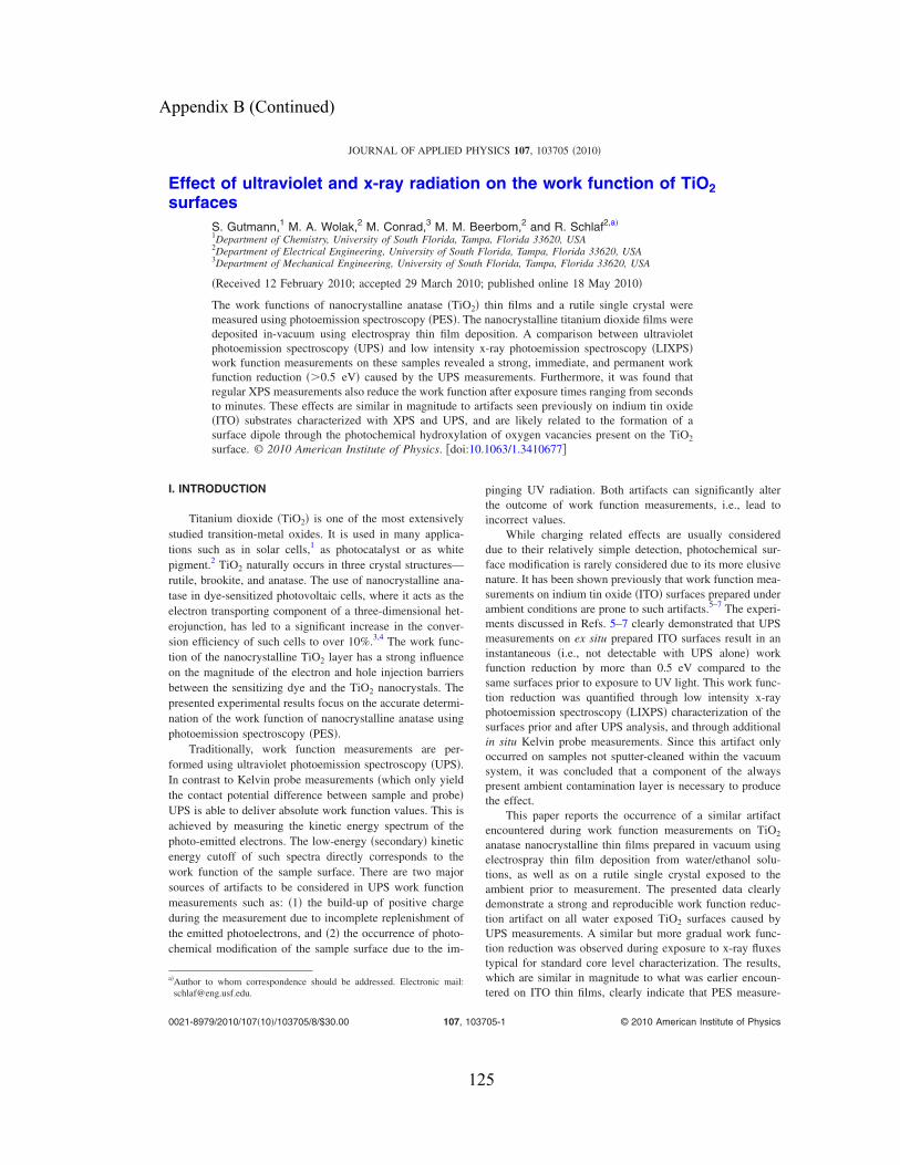
Effect of ultraviolet and x-ray radiation on the work function of TiO2surfaces
S. Gutmann,1 M. A. Wolak,2 M. Conrad,3 M. M. Beerbom,2 and R. Schlaf2,a�
1Department of Chemistry, University of South Florida, Tampa, Florida 33620, USA2Department of Electrical Engineering, University of South Florida, Tampa, Florida 33620, USA3Department of Mechanical Engineering, University of South Florida, Tampa, Florida 33620, USA
�Received 12 February 2010; accepted 29 March 2010; published online 18 May 2010�
The work functions of nanocrystalline anatase �TiO2� thin films and a rutile single crystal weremeasured using photoemission spectroscopy �PES�. The nanocrystalline titanium dioxide films weredeposited in-vacuum using electrospray thin film deposition. A comparison between ultravioletphotoemission spectroscopy �UPS� and low intensity x-ray photoemission spectroscopy �LIXPS�work function measurements on these samples revealed a strong, immediate, and permanent workfunction reduction ��0.5 eV� caused by the UPS measurements. Furthermore, it was found thatregular XPS measurements also reduce the work function after exposure times ranging from secondsto minutes. These effects are similar in magnitude to artifacts seen previously on indium tin oxide�ITO� substrates characterized with XPS and UPS, and are likely related to the formation of asurface dipole through the photochemical hydroxylation of oxygen vacancies present on the TiO2
surface. © 2010 American Institute of Physics. �doi:10.1063/1.3410677�
I. INTRODUCTION
Titanium dioxide �TiO2� is one of the most extensivelystudied transition-metal oxides. It is used in many applica-tions such as in solar cells,1 as photocatalyst or as whitepigment.2 TiO2 naturally occurs in three crystal structures—rutile, brookite, and anatase. The use of nanocrystalline ana-tase in dye-sensitized photovoltaic cells, where it acts as theelectron transporting component of a three-dimensional het-erojunction, has led to a significant increase in the conver-sion efficiency of such cells to over 10%.3,4 The work func-tion of the nanocrystalline TiO2 layer has a strong influenceon the magnitude of the electron and hole injection barriersbetween the sensitizing dye and the TiO2 nanocrystals. Thepresented experimental results focus on the accurate determi-nation of the work function of nanocrystalline anatase usingphotoemission spectroscopy �PES�.
Traditionally, work function measurements are per-formed using ultraviolet photoemission spectroscopy �UPS�.In contrast to Kelvin probe measurements �which only yieldthe contact potential difference between sample and probe�UPS is able to deliver absolute work function values. This isachieved by measuring the kinetic energy spectrum of thephoto-emitted electrons. The low-energy �secondary� kineticenergy cutoff of such spectra directly corresponds to thework function of the sample surface. There are two majorsources of artifacts to be considered in UPS work functionmeasurements such as: �1� the build-up of positive chargeduring the measurement due to incomplete replenishment ofthe emitted photoelectrons, and �2� the occurrence of photo-chemical modification of the sample surface due to the im-
pinging UV radiation. Both artifacts can significantly alterthe outcome of work function measurements, i.e., lead toincorrect values.
While charging related effects are usually considereddue to their relatively simple detection, photochemical sur-face modification is rarely considered due to its more elusivenature. It has been shown previously that work function mea-surements on indium tin oxide �ITO� surfaces prepared underambient conditions are prone to such artifacts.5–7 The experi-ments discussed in Refs. 5–7 clearly demonstrated that UPSmeasurements on ex situ prepared ITO surfaces result in aninstantaneous �i.e., not detectable with UPS alone� workfunction reduction by more than 0.5 eV compared to thesame surfaces prior to exposure to UV light. This work func-tion reduction was quantified through low intensity x-rayphotoemission spectroscopy �LIXPS� characterization of thesurfaces prior and after UPS analysis, and through additionalin situ Kelvin probe measurements. Since this artifact onlyoccurred on samples not sputter-cleaned within the vacuumsystem, it was concluded that a component of the alwayspresent ambient contamination layer is necessary to producethe effect.
This paper reports the occurrence of a similar artifactencountered during work function measurements on TiO2
anatase nanocrystalline thin films prepared in vacuum usingelectrospray thin film deposition from water/ethanol solu-tions, as well as on a rutile single crystal exposed to theambient prior to measurement. The presented data clearlydemonstrate a strong and reproducible work function reduc-tion artifact on all water exposed TiO2 surfaces caused byUPS measurements. A similar but more gradual work func-tion reduction was observed during exposure to x-ray fluxestypical for standard core level characterization. The results,which are similar in magnitude to what was earlier encoun-tered on ITO thin films, clearly indicate that PES measure-
a�Author to whom correspondence should be addressed. Electronic mail:[email protected].
JOURNAL OF APPLIED PHYSICS 107, 103705 �2010�
0021-8979/2010/107�10�/103705/8/$30.00 © 2010 American Institute of Physics107, 103705-1
Author complimentary copy. Redistribution subject to AIP license or copyright, see http://jap.aip.org/jap/copyright.jsp
Appendix B (Continued)
125
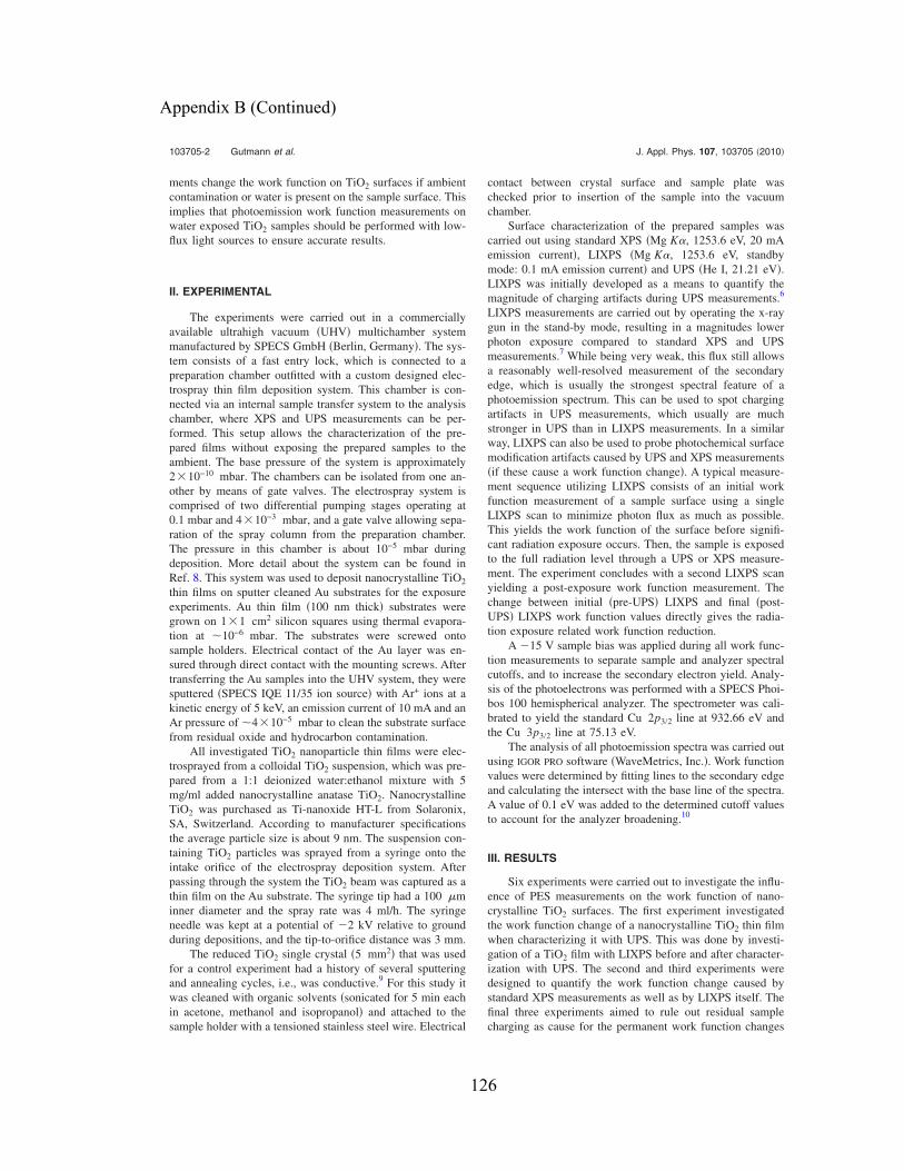
ments change the work function on TiO2 surfaces if ambientcontamination or water is present on the sample surface. Thisimplies that photoemission work function measurements onwater exposed TiO2 samples should be performed with low-flux light sources to ensure accurate results.
II. EXPERIMENTAL
The experiments were carried out in a commerciallyavailable ultrahigh vacuum �UHV� multichamber systemmanufactured by SPECS GmbH �Berlin, Germany�. The sys-tem consists of a fast entry lock, which is connected to apreparation chamber outfitted with a custom designed elec-trospray thin film deposition system. This chamber is con-nected via an internal sample transfer system to the analysischamber, where XPS and UPS measurements can be per-formed. This setup allows the characterization of the pre-pared films without exposing the prepared samples to theambient. The base pressure of the system is approximately2�10−10 mbar. The chambers can be isolated from one an-other by means of gate valves. The electrospray system iscomprised of two differential pumping stages operating at0.1 mbar and 4�10−3 mbar, and a gate valve allowing sepa-ration of the spray column from the preparation chamber.The pressure in this chamber is about 10−5 mbar duringdeposition. More detail about the system can be found inRef. 8. This system was used to deposit nanocrystalline TiO2
thin films on sputter cleaned Au substrates for the exposureexperiments. Au thin film �100 nm thick� substrates weregrown on 1�1 cm2 silicon squares using thermal evapora-tion at �10−6 mbar. The substrates were screwed ontosample holders. Electrical contact of the Au layer was en-sured through direct contact with the mounting screws. Aftertransferring the Au samples into the UHV system, they weresputtered �SPECS IQE 11/35 ion source� with Ar+ ions at akinetic energy of 5 keV, an emission current of 10 mA and anAr pressure of �4�10−5 mbar to clean the substrate surfacefrom residual oxide and hydrocarbon contamination.
All investigated TiO2 nanoparticle thin films were elec-trosprayed from a colloidal TiO2 suspension, which was pre-pared from a 1:1 deionized water:ethanol mixture with 5mg/ml added nanocrystalline anatase TiO2. NanocrystallineTiO2 was purchased as Ti-nanoxide HT-L from Solaronix,SA, Switzerland. According to manufacturer specificationsthe average particle size is about 9 nm. The suspension con-taining TiO2 particles was sprayed from a syringe onto theintake orifice of the electrospray deposition system. Afterpassing through the system the TiO2 beam was captured as athin film on the Au substrate. The syringe tip had a 100 �minner diameter and the spray rate was 4 ml/h. The syringeneedle was kept at a potential of �2 kV relative to groundduring depositions, and the tip-to-orifice distance was 3 mm.
The reduced TiO2 single crystal �5 mm2� that was usedfor a control experiment had a history of several sputteringand annealing cycles, i.e., was conductive.9 For this study itwas cleaned with organic solvents �sonicated for 5 min eachin acetone, methanol and isopropanol� and attached to thesample holder with a tensioned stainless steel wire. Electrical
contact between crystal surface and sample plate waschecked prior to insertion of the sample into the vacuumchamber.
Surface characterization of the prepared samples wascarried out using standard XPS �Mg K�, 1253.6 eV, 20 mAemission current�, LIXPS �Mg K�, 1253.6 eV, standbymode: 0.1 mA emission current� and UPS �He I, 21.21 eV�.LIXPS was initially developed as a means to quantify themagnitude of charging artifacts during UPS measurements.6
LIXPS measurements are carried out by operating the x-raygun in the stand-by mode, resulting in a magnitudes lowerphoton exposure compared to standard XPS and UPSmeasurements.7 While being very weak, this flux still allowsa reasonably well-resolved measurement of the secondaryedge, which is usually the strongest spectral feature of aphotoemission spectrum. This can be used to spot chargingartifacts in UPS measurements, which usually are muchstronger in UPS than in LIXPS measurements. In a similarway, LIXPS can also be used to probe photochemical surfacemodification artifacts caused by UPS and XPS measurements�if these cause a work function change�. A typical measure-ment sequence utilizing LIXPS consists of an initial workfunction measurement of a sample surface using a singleLIXPS scan to minimize photon flux as much as possible.This yields the work function of the surface before signifi-cant radiation exposure occurs. Then, the sample is exposedto the full radiation level through a UPS or XPS measure-ment. The experiment concludes with a second LIXPS scanyielding a post-exposure work function measurement. Thechange between initial �pre-UPS� LIXPS and final �post-UPS� LIXPS work function values directly gives the radia-tion exposure related work function reduction.
A �15 V sample bias was applied during all work func-tion measurements to separate sample and analyzer spectralcutoffs, and to increase the secondary electron yield. Analy-sis of the photoelectrons was performed with a SPECS Phoi-bos 100 hemispherical analyzer. The spectrometer was cali-brated to yield the standard Cu 2p3/2 line at 932.66 eV andthe Cu 3p3/2 line at 75.13 eV.
The analysis of all photoemission spectra was carried outusing IGOR PRO software �WaveMetrics, Inc.�. Work functionvalues were determined by fitting lines to the secondary edgeand calculating the intersect with the base line of the spectra.A value of 0.1 eV was added to the determined cutoff valuesto account for the analyzer broadening.10
III. RESULTS
Six experiments were carried out to investigate the influ-ence of PES measurements on the work function of nano-crystalline TiO2 surfaces. The first experiment investigatedthe work function change of a nanocrystalline TiO2 thin filmwhen characterizing it with UPS. This was done by investi-gation of a TiO2 film with LIXPS before and after character-ization with UPS. The second and third experiments weredesigned to quantify the work function change caused bystandard XPS measurements as well as by LIXPS itself. Thefinal three experiments aimed to rule out residual samplecharging as cause for the permanent work function changes
103705-2 Gutmann et al. J. Appl. Phys. 107, 103705 �2010�
Author complimentary copy. Redistribution subject to AIP license or copyright, see http://jap.aip.org/jap/copyright.jsp
Appendix B (Continued)
126
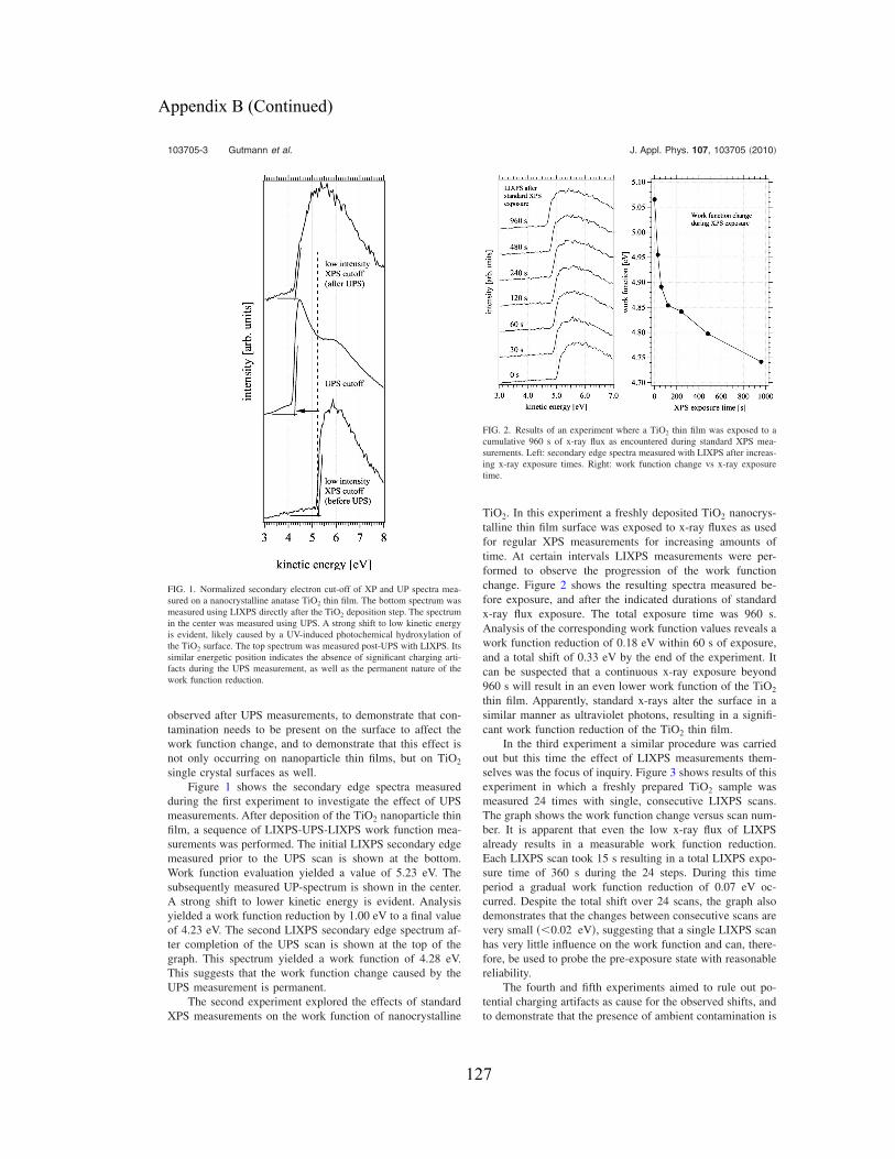
observed after UPS measurements, to demonstrate that con-tamination needs to be present on the surface to affect thework function change, and to demonstrate that this effect isnot only occurring on nanoparticle thin films, but on TiO2
single crystal surfaces as well.Figure 1 shows the secondary edge spectra measured
during the first experiment to investigate the effect of UPSmeasurements. After deposition of the TiO2 nanoparticle thinfilm, a sequence of LIXPS-UPS-LIXPS work function mea-surements was performed. The initial LIXPS secondary edgemeasured prior to the UPS scan is shown at the bottom.Work function evaluation yielded a value of 5.23 eV. Thesubsequently measured UP-spectrum is shown in the center.A strong shift to lower kinetic energy is evident. Analysisyielded a work function reduction by 1.00 eV to a final valueof 4.23 eV. The second LIXPS secondary edge spectrum af-ter completion of the UPS scan is shown at the top of thegraph. This spectrum yielded a work function of 4.28 eV.This suggests that the work function change caused by theUPS measurement is permanent.
The second experiment explored the effects of standardXPS measurements on the work function of nanocrystalline
TiO2. In this experiment a freshly deposited TiO2 nanocrys-talline thin film surface was exposed to x-ray fluxes as usedfor regular XPS measurements for increasing amounts oftime. At certain intervals LIXPS measurements were per-formed to observe the progression of the work functionchange. Figure 2 shows the resulting spectra measured be-fore exposure, and after the indicated durations of standardx-ray flux exposure. The total exposure time was 960 s.Analysis of the corresponding work function values reveals awork function reduction of 0.18 eV within 60 s of exposure,and a total shift of 0.33 eV by the end of the experiment. Itcan be suspected that a continuous x-ray exposure beyond960 s will result in an even lower work function of the TiO2
thin film. Apparently, standard x-rays alter the surface in asimilar manner as ultraviolet photons, resulting in a signifi-cant work function reduction of the TiO2 thin film.
In the third experiment a similar procedure was carriedout but this time the effect of LIXPS measurements them-selves was the focus of inquiry. Figure 3 shows results of thisexperiment in which a freshly prepared TiO2 sample wasmeasured 24 times with single, consecutive LIXPS scans.The graph shows the work function change versus scan num-ber. It is apparent that even the low x-ray flux of LIXPSalready results in a measurable work function reduction.Each LIXPS scan took 15 s resulting in a total LIXPS expo-sure time of 360 s during the 24 steps. During this timeperiod a gradual work function reduction of 0.07 eV oc-curred. Despite the total shift over 24 scans, the graph alsodemonstrates that the changes between consecutive scans arevery small ��0.02 eV�, suggesting that a single LIXPS scanhas very little influence on the work function and can, there-fore, be used to probe the pre-exposure state with reasonablereliability.
The fourth and fifth experiments aimed to rule out po-tential charging artifacts as cause for the observed shifts, andto demonstrate that the presence of ambient contamination is
FIG. 1. Normalized secondary electron cut-off of XP and UP spectra mea-sured on a nanocrystalline anatase TiO2 thin film. The bottom spectrum wasmeasured using LIXPS directly after the TiO2 deposition step. The spectrumin the center was measured using UPS. A strong shift to low kinetic energyis evident, likely caused by a UV-induced photochemical hydroxylation ofthe TiO2 surface. The top spectrum was measured post-UPS with LIXPS. Itssimilar energetic position indicates the absence of significant charging arti-facts during the UPS measurement, as well as the permanent nature of thework function reduction.
FIG. 2. Results of an experiment where a TiO2 thin film was exposed to acumulative 960 s of x-ray flux as encountered during standard XPS mea-surements. Left: secondary edge spectra measured with LIXPS after increas-ing x-ray exposure times. Right: work function change vs x-ray exposuretime.
103705-3 Gutmann et al. J. Appl. Phys. 107, 103705 �2010�
Author complimentary copy. Redistribution subject to AIP license or copyright, see http://jap.aip.org/jap/copyright.jsp
Appendix B (Continued)
127
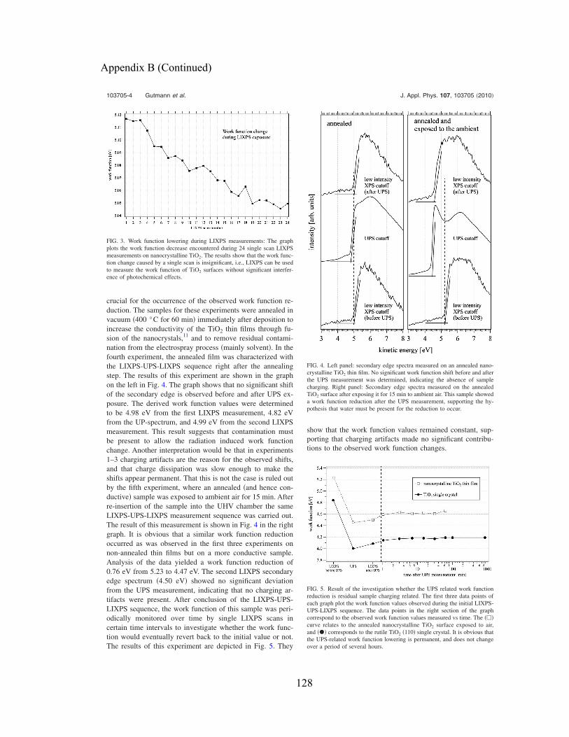
crucial for the occurrence of the observed work function re-duction. The samples for these experiments were annealed invacuum �400 °C for 60 min� immediately after deposition toincrease the conductivity of the TiO2 thin films through fu-sion of the nanocrystals,11 and to remove residual contami-nation from the electrospray process �mainly solvent�. In thefourth experiment, the annealed film was characterized withthe LIXPS-UPS-LIXPS sequence right after the annealingstep. The results of this experiment are shown in the graphon the left in Fig. 4. The graph shows that no significant shiftof the secondary edge is observed before and after UPS ex-posure. The derived work function values were determinedto be 4.98 eV from the first LIXPS measurement, 4.82 eVfrom the UP-spectrum, and 4.99 eV from the second LIXPSmeasurement. This result suggests that contamination mustbe present to allow the radiation induced work functionchange. Another interpretation would be that in experiments1–3 charging artifacts are the reason for the observed shifts,and that charge dissipation was slow enough to make theshifts appear permanent. That this is not the case is ruled outby the fifth experiment, where an annealed �and hence con-ductive� sample was exposed to ambient air for 15 min. Afterre-insertion of the sample into the UHV chamber the sameLIXPS-UPS-LIXPS measurement sequence was carried out.The result of this measurement is shown in Fig. 4 in the rightgraph. It is obvious that a similar work function reductionoccurred as was observed in the first three experiments onnon-annealed thin films but on a more conductive sample.Analysis of the data yielded a work function reduction of0.76 eV from 5.23 to 4.47 eV. The second LIXPS secondaryedge spectrum �4.50 eV� showed no significant deviationfrom the UPS measurement, indicating that no charging ar-tifacts were present. After conclusion of the LIXPS-UPS-LIXPS sequence, the work function of this sample was peri-odically monitored over time by single LIXPS scans incertain time intervals to investigate whether the work func-tion would eventually revert back to the initial value or not.The results of this experiment are depicted in Fig. 5. They
show that the work function values remained constant, sup-porting that charging artifacts made no significant contribu-tions to the observed work function changes.
FIG. 3. Work function lowering during LIXPS measurements: The graphplots the work function decrease encountered during 24 single scan LIXPSmeasurements on nanocrystalline TiO2. The results show that the work func-tion change caused by a single scan is insignificant, i.e., LIXPS can be usedto measure the work function of TiO2 surfaces without significant interfer-ence of photochemical effects.
FIG. 4. Left panel: secondary edge spectra measured on an annealed nano-crystalline TiO2 thin film. No significant work function shift before and afterthe UPS measurement was determined, indicating the absence of samplecharging. Right panel: Secondary edge spectra measured on the annealedTiO2 surface after exposing it for 15 min to ambient air. This sample showeda work function reduction after the UPS measurement, supporting the hy-pothesis that water must be present for the reduction to occur.
FIG. 5. Result of the investigation whether the UPS related work functionreduction is residual sample charging related. The first three data points ofeach graph plot the work function values observed during the initial LIXPS-UPS-LIXPS sequence. The data points in the right section of the graphcorrespond to the observed work function values measured vs time. The ���curve relates to the annealed nanocrystalline TiO2 surface exposed to air,and ��� corresponds to the rutile TiO2 �110� single crystal. It is obvious thatthe UPS-related work function lowering is permanent, and does not changeover a period of several hours.
103705-4 Gutmann et al. J. Appl. Phys. 107, 103705 �2010�
Author complimentary copy. Redistribution subject to AIP license or copyright, see http://jap.aip.org/jap/copyright.jsp
Appendix B (Continued)
128
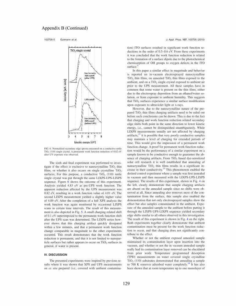
The sixth and final experiment was performed to inves-tigate if the effect is exclusive to nanocrystalline TiO2 thinfilms, or whether it also occurs on single crystalline TiO2
surfaces. For this purpose, a conductive TiO2 �110� rutilesingle crystal was put through the same LIXPS-UPS-LIXPSsequence. Figure 6 shows the outcome of this experiment.Analysis yielded 4.83 eV as pre-UPS work function. Theapparent reduction affected by the UPS measurement was0.82 eV, resulting in a work function value of 4.01 eV. Thesecond LIXPS measurement yielded a slightly higher valueof 4.09 eV. After the completion of a full XPS analysis thework function was again monitored by occasional LIXPSscans in certain time intervals. The result of this measure-ment is also depicted in Fig. 5. A small charging related shiftof 0.1 eV superimposed to the permanent work function shiftafter the UPS scan was determined. The LIXPS series how-ever shows that this charging artifact quickly dissipatedwithin a few minutes, and that a permanent work functionchange comparable in magnitude to the other experimentsoccurred. This result demonstrates that the work functionreduction is permanent, and that it is not limited to nanopar-ticle surfaces but rather appears to occur on TiO2 surfaces ingeneral, if water is present.
IV. DISCUSSION
The presented experiments were inspired by previous re-sults where it was shown that XPS and UPS measurementson ex situ prepared �i.e., covered with ambient contamina-
tion� ITO surfaces resulted in significant work function re-ductions in the order of 0.5–0.6 eV. From these experimentsit was concluded that the work function reduction is relatedto the formation of a surface dipole due to the photochemicalchemisorption of OH groups to oxygen defects in the ITOsurface.5
In this paper a similar effect in magnitude and behavioris reported on in-vacuum electrosprayed nanocrystallineTiO2 thin films, on annealed TiO2 thin films exposed to theambient, and on a TiO2 single crystal exposed to ambient airprior to the UPS measurement. All these samples have incommon that some water is present on the thin films, eitherdue to the electrospray deposition from an ethanol/water so-lution, or from exposure to ambient humidity. This suggeststhat TiO2 surfaces experience a similar surface modificationupon exposure to ultraviolet light or x-rays.
However, due to the nanocrystalline nature of the pre-pared TiO2 thin films charging artifacts need to be ruled outbefore such conclusions can be drawn. This is due to the factthat charging and work function reduction related secondaryedge shifts both point in the same direction to lower kineticenergy, i.e., cannot be distinguished unambiguously. WhileLIXPS measurements usually are not affected by chargingartifacts,12 it is possible that very poorly conductive samplesmay maintain a level of charging for extended periods oftime. This would give the impression of a permanent workfunction change. A proof for permanent work function reduc-tion would be the performance of a similar experiment on asample known to be conductive enough to guarantee the ab-sence of charging artifacts. From TiO2 based dye-sensitizedsolar cell research it is well established that annealing ofnanocrystalline TiO2 thin films results in a significant in-crease in their conductivity.13 This phenomenon enabled thedesired control experiment where a sample was first annealedin vacuum and then measured with the LIXPS-UPS-LIXPSsequence. The results of this experiment, shown in Fig. 4 onthe left, clearly demonstrate that sample charging artifactsare absent on the annealed sample since no shifts were ob-served at all. Since annealing also removes most of the con-tamination from the surface, this sample also enabled thedemonstration that not only electrosprayed samples show theeffect but also samples contaminated in the ambient. Expo-sure of the annealed sample to the ambient before putting itthrough the LIXPS-UPS-LIXPS sequence yielded secondaryedge shifts similar to all others observed in this investigation.The result of this experiment is shown in Fig. 4 on the right.Both experiments together clearly demonstrate that ambientcontamination must be present for the work function reduc-tion to occur, and that charging does not significantly con-tribute to the effect.
Whether or not the ambient exposed annealed samplemaintained its contamination layer upon insertion into thevacuum, and whether or not the in vacuum annealed samplereally had its contamination layer removed can be elucidatedfrom prior work: Temperature programmed desorption�TPD� measurements on water covered single crystallineTiO2 �110� substrates demonstrated that annealing a sampleto 700 K removes adsorbed water completely.14 It has alsobeen shown that at room temperature up to one monolayer of
FIG. 6. Normalized secondary edge spectra measured on a conductive rutileTiO2 �110� single crystal. A permanent work function reduction of 0.82 eVafter UV exposure was observed.
103705-5 Gutmann et al. J. Appl. Phys. 107, 103705 �2010�
Author complimentary copy. Redistribution subject to AIP license or copyright, see http://jap.aip.org/jap/copyright.jsp
Appendix B (Continued)
129
adsorbed water is stable on the TiO2 surface in vacuum.15
The same appears to hold for nanocrystalline TiO2, whichalso yields a water related TPD peak at and above roomtemperature.16 In light of these reports, it is reasonable toconclude that the investigated TiO2 samples are indeed cov-ered with up to one monolayer of water molecules directlyafter electrospray deposition or exposure to the ambient.
The permanence of the observed work function reduc-tion is also demonstrated by the long term work functionmonitoring that was carried out after completion of the initialLIXPS-UPS-LIXPS sequences on the annealed nanocrystal-line film that was exposed to the ambient, and the rutilesingle crystal. In these experiments, the work function wasmonitored over several hundred minutes after the initial mea-surements by carrying out single LIXPS scans in certain timeintervals. Figure 5 plots the work function values of bothsamples ��: electrosprayed nanocrystalline TiO2; �: singlecrystalline TiO2 �110�� versus time. It is obvious that thework function after the UPS measurements remained con-stant. Both samples showed a small amount of superimposedresidual sample charging artifacts after the UPS measure-ments, which completely dissipated after two minutes. Thisis evident from the approximately 0.1 eV work function in-crease immediately after the UPS measurements before aconstant value is assumed. The relative work function reduc-tions observed on both samples are very similar, while theinitial work function values are different. The nanocrystallinefilm showed a larger work function of 5.23 eV, with thesingle crystal exhibiting a smaller value of 4.83 eV. It is notentirely clear what causes this difference but it is reasonableto suspect the drastically different surface structures of bothsamples.
A considerable number of reports have focused on thedissociation of water on TiO2.17 Even though the rutile TiO2
�110� surface has become one of the key model systems formetal oxide surfaces, it is not completely clear how and whywater molecules dissociate on the TiO2 �110� surface. Hen-rich et al.18 and Kurtz et al.19 have shown that dominantdefects on TiO2 surfaces are oxygen vacancies but it is be-lieved that pervasive defects are bridging oxygen vacancies.It is currently assumed that the oxide surface reactivity isdominated by these defective states. There is strong experi-mental and theoretical evidence, STM studies being the mostrecent ones,20–22 that water dissociates and hydroxylates thesurface,2,17,19 leaving bridging OH groups behind.
The secondary edge spectra shown in Fig. 6 demonstratethat the work function reduction can also be observed on aTiO2 �110� single crystal surface. The shift of 0.82 eV tolower kinetic energy is similar to the shift determined on thenanocrystalline films. This supposes that the underlyingmechanism for the work function shift is likely similar forboth systems.
With regard to the work function lowering mechanism, itcan be hypothesized that the UV radiation leads to a photo-chemical hydroxylation of oxygen defect sites due to thepresence of water residues on the surface of the TiO2. Thephotochemical dissociation of water is supported by a reportby Henrich et al.18 where a work function reduction in simi-lar magnitude was seen on ion-bombarded single crystalline
TiO2 �110�. The experiments in Ref. 18 showed that increas-ing exposure of the sputtered surface to water vapor leakedinto the vacuum chamber resulted in a gradual reduction ofthe work function by about 0.5–0.6 eV. It was concluded thatwater molecules dissociatively chemisorb at oxygen vacan-cies, resulting in the attachment of OH groups. Furtheranalysis of their data allowed the conclusion that the orien-tation of the OH groups is mostly perpendicular to the sur-face, explaining the build-up of a work function loweringsurface dipole �the more electropositive hydrogen atomscause an excess of positive charge on the outside of the sur-face�. Assuming the ion bombardment caused a disorderedsurface similar to a surface composed of TiO2 nanocrystals,it can be reasoned that the observed work function reductionon nanocrystalline TiO2 films is likely also caused by thedissociative desorption of water. Similar results have beenrecently published by Marques et al.23 and Onda et al.24 Itwas reported that secondary edges shift to lower kinetic en-ergy �up to 1.2 eV� with increasing partial pressure of water.However, in difference to the conclusions drawn in Refs. 18,23, and 24, the results presented here suggest that the hy-droxylation process is not solely caused by the presence ofdefects but rather is a photochemical process caused by theUV exposure during the measurement itself.
Experiments by Gravelle et al.25 and Shultz et al.,26 whodemonstrated that ultraviolet photons create stable Ti3+ de-fects in UHV on nearly perfect TiO2 �110� single crystalsurfaces, suggest that UV radiation during UP spectroscopicmeasurements may also cause the photoinduced generationof �additional� oxygen vacancies. Therefore, it appears rea-sonable to consider that the work function reduction is theresult of the interaction between pre-existing as well as photogenerated Ti3+ species and the dissociation of water mol-ecules on these active sites, resulting in an increased concen-tration of hydroxyl groups on the surface.
This conclusion, i.e., that the dissociative chemisorptionprocess is in fact a photochemical process, is further sup-ported by research on photochemical water splitting on TiO2
surfaces. While continuous photochemical water splitting ap-pears to require the presence of additional Pt catalysts at theTiO2 surface, it has been shown that water already photo-chemically reacts with oxygen vacancies on pure TiO2 sur-faces with above-band gap �UV� illumination. Van Dammeand Hall,27 as well as Sato and White28 demonstrated thatTiO2 surfaces exposed to water vapor lead to the productionof a finite amount of H2 but only under continuous UV illu-mination. It was concluded that the process involves a one-time passivation of a defined number of Ti3+ oxygen vacan-cies in the TiO2 surface with hydroxyl-groups provided bythe photochemical dissociation of water.
In the case of the electrosprayed TiO2 thin films it isnecessary to consider the additional presence of ethanol mol-ecules �except on the annealed samples�. Investigations bySauer and Ollis,29 and by Muggli et al.,30 indicate that etha-nol is photocatalytically oxidized by above-band gap illumi-nation yielding CO2 and water as final reaction products. Atthe same time there is evidence that water plays a competi-tive role with regard to ethanol adsorption on the TiO2
surface.31 Combined, these findings suggest that any ethanol
103705-6 Gutmann et al. J. Appl. Phys. 107, 103705 �2010�
Author complimentary copy. Redistribution subject to AIP license or copyright, see http://jap.aip.org/jap/copyright.jsp
Appendix B (Continued)
130
present on the surface during UV exposure was probablyconverted to water, which then subsequently participated inthe hydroxylation of the Ti3+ oxygen vacancies, further con-tributing to the formation of the detected surface dipole.
The ultimate proof for the above conclusions would bethe direct detection of OH groups after UPS measurements.Unfortunately, a direct detection of adsorbed hydroxyl-groups via O 1s emissions proved difficult not only due tothe dominant and broad O 1s emission feature related to thenanocrystalline TiO2 film but also due to the fact that thepresented experiments demonstrate that XPS measurementsthemselves already cause the photochemical dissociativechemisorption process. This indicates that any XPS measure-ments using standard x-ray flux strengths can only yield theend state of the reaction but not the state before chemisorp-tion. In the presented experiments standard x-ray exposureyielded a work function reduction of 0.33 eV after 960 s�Fig. 2�. Significant shifts are already observed after muchshorter exposure times of the order of 30 s. Considering thetime it takes to measure a reasonably well resolved XPSspectrum, this makes it virtually impossible to measure thestate of the surface before any significant water chemisorp-tion. Core level measurements of the Ti 2p peak performedin conjunction with the discussed experiments all showed theabsence of Ti3+ indicating a full oxidation of the surface. Aneffort was made to try measure the Ti 2p emission line withvery low x-ray exposure but this yielded very noisy spectra,which could not be evaluated conclusively. The only photo-emission measurement able to show the state of the surfacebefore the reaction is LIXPS. This was confirmed by theexploration of the effect of low intensity x-ray flux as em-ployed during LIXPS measurements �Fig. 3�. These experi-ments showed that single scans LIXPS measurements can besuccessfully used to measure the surface before significantchemisorption occurs; however the low x-ray flux limits thistechnique to work function measurements. Yi et al.7 esti-mated the photon flux on the sample during LIXPS measure-ments only amounts to about 1% of the photon flux encoun-tered during XPS measurements. In contrast, the photon fluxof modern UV sources is about three magnitudes higher thanthat of a typical x-ray gun, which explains the immediatemaximum work function shift caused by a single scan UPSmeasurement. In summary, these results clearly demonstratethat single scan LIXPS measurements result in reliable workfunction values with an absolute accuracy better than �0.1eV. They also suggest that XPS and UPS measurements, dueto the high photon fluxes, can only yield the state of thealready photochemically altered surface.
These conclusions suggest that several earlier reports ofPES measurements concerned with water adsorption on TiO2
surfaces may have overlooked the occurrence of photo-chemical effects caused by the measurement process itself.For example, a recently published experiment on sputteredTiO2 �110� single crystalline surfaces32 reported that oxygenvacancies are fully passivated at 420 K when water vapor isintroduced into the vacuum system. In this experiment theTi 2p3/2 XPS emission line showed a distinct shoulder atabout 457 eV corresponding to Ti3+ and Ti2+ before waterwas introduced. After water exposure, this shoulder vanished
leaving a single emission line at about 459 eV, indicating fullconversion to Ti4+, which is characteristic of bulk Ti in TiO2.It was concluded that water auto-dissociates at the defectsites, while a photochemical dissociation may have occurredduring the measurement instead. Another example is a paperby Orendorz et al.33 where the absence of Ti3+ states in XPScore-level measurements on in-ambient sol-gel and spray-prepared nanocrystalline TiO2 films was interpreted as ab-sence of a significant amount of defects. Instead x-ray expo-sure might have caused the photoinduced hydroxylation ofTi3+ defect states during the XPS core-level measurements,giving the impression of a low defect density.
V. CONCLUSION
In summary, the discussed experiments demonstrate thatUV and x-ray fluxes encountered during typical UPS andXPS measurements significantly ��0.5 eV� reduce the workfunction of nanocrystalline TiO2 thin films and rutile singlecrystals when water is present on the surface. The mostlikely mechanism of this phenomenon appears to be the for-mation of a surface dipole caused by the photochemical hy-droxylation of oxygen vacancies in the TiO2 surface. Thisimplies that standard UPS measurements cannot yield reli-able work function values on such samples. This artifact wasdemonstrated using LIXPS work function measurements,which expose the sample to a magnitudes lower photon fluxthan standard UPS measurements, thus enabling the detec-tion of the work function reduction by the UPS measure-ments. Additional experiments showed that x-ray fluxes en-countered during standard core level XPS measurements alsocause this effect. These results suggest that care must betaken when investigating the interaction between water andTiO2 surfaces with PES, since it is likely that photochemicalhydroxylation will always occur to some degree caused bythe measurement itself. LIXPS work function measurementsoffer a way to detect the occurrence of this artifact.
ACKNOWLEDGMENTS
The authors gratefully acknowledge funding by the Na-tional Science Foundation �Grant Nos. NSF DMR-0906922and ECCS-0701861�. They also thank Dr. Matthias Batzill ofthe Department of Physics at the University of South Floridafor helpful discussions and for providing the TiO2 �110�single crystal. MC is grateful for partial support through theUSF College of Engineering Research Experience for Under-graduates program.
1N. G. Park, J. van de Lagemaat, and A. J. Frank, J. Phys. Chem. B 104,8989 �2000�.
2U. Diebold, Surf. Sci. Rep. 48, 53 �2003�.3M. Grätzel, J. Photochem. Photobiol. C 4, 145 �2003�.4S. Ito, T. N. Murakami, P. Comte, P. Liska, C. Grätzel, M. K. Nazeeruddin,and M. Grätzel, Thin Solid Films 516, 4613 �2008�.
5M. M. Beerbom, B. Lägel, A. J. Cascio, B. V. Doran, and R. Schlaf, J.Electron Spectrosc. Relat. Phenom. 152, 12 �2006�.
6R. Schlaf, H. Murata, and Z. H. Kafafi, J. Electron Spectrosc. Relat. Phe-nom. 120, 149 �2001�.
7Y. Yi, J. E. Lyon, M. M. Beerbom, and R. Schlaf, J. Appl. Phys. 100,093719 �2006�.
8N. Dam, M. M. Beerbom, J. C. Braunagel, and R. Schlaf, J. Appl. Phys.97, 024909 �2005�.
103705-7 Gutmann et al. J. Appl. Phys. 107, 103705 �2010�
Author complimentary copy. Redistribution subject to AIP license or copyright, see http://jap.aip.org/jap/copyright.jsp
Appendix B (Continued)
131
9M. Li, W. Hebenstreit, U. Diebold, A. M. Tyryshkin, M. K. Bowman, G.G. Dunham, and M. A. Henderson, J. Phys. Chem. B 104, 4944 �2000�.
10R. Schlaf, P. G. Schroeder, M. W. Nelson, B. A. Parkinson, C. D. Merritt,L. A. Crisafulli, H. Murata, and Z. H. Kafafi, Surf. Sci. 450, 142 �2000�.
11N. R. Mathews, E. R. Morales, M. A. Cortés-Jacome, and J. A. T. Anto-nio, Sol. Energy 83, 1499 �2009�.
12R. Schlaf, C. D. Merritt, L. A. Crisafulli, and Z. H. Kafafi, J. Appl. Phys.86, 5678 �1999�.
13A. Hagfeldt and M. Grätzel, Chem. Rev. 95, 49 �1995�.14M. B. Hugenschmidt, L. Gamble, and C. T. Campbell, Surf. Sci. 302, 329
�1994�.15D. Brinkley, M. Dietrich, T. Engel, P. Farrall, G. Gantner, A. Schafer, and
A. Szuchmacher, Surf. Sci. 395, 292 �1998�.16V. M. Gun’ko, J. P. Blitz, V. I. Zarko, V. V. Turov, E. M. Pakhlov, O. I.
Oranska, E. V. Goncharuk, Y. I. Gornikov, V. S. Sergeev, T. V. Kulik, B.B. Palyanytsya, and R. K. Samala, J. Colloid Interface Sci. 330, 125�2009�.
17M. A. Henderson, Surf. Sci. Rep. 46, 1 �2002�.18V. E. Henrich, G. Dresselhaus, and H. J. Zeiger, Solid State Commun. 24,
623 �1977�.19R. L. Kurtz, R. Stockbauer, T. E. Madey, E. Roman, and J. L. Desegovia,
Surf. Sci. 218, 178 �1989�.20I. M. Brookes, C. A. Muryn, and G. Thornton, Phys. Rev. Lett. 87, 266103
�2001�.21R. Schaub, R. Thostrup, N. Lopez, E. Laegsgaard, I. Stensgaard, J. K.
Norskov, and F. Besenbacher, Phys. Rev. Lett. 87, 266104 �2001�.22Z. Zhang, O. Bondarchuk, B. D. Kay, J. M. White, and Z. Dohnálek, J.
Phys. Chem. B 110, 21840 �2006�.23H. P. Marques, A. R. Canário, A. M. C. Moutinho, and O. Teodoro, Appl.
Surf. Sci. 255, 7389 �2009�.24K. Onda, B. Li, and H. Petek, Phys. Rev. B 70, 045415 �2004�.25P. C. Gravelle, F. Juillet, P. Meriaudeau, and S. J. Teichner, Discuss. Far-
aday Soc. 52, 140 �1971�.26A. N. Shultz, W. Jang, W. M. Hetherington, D. R. Baer, L. Q. Wang, and
M. H. Engelhard, Surf. Sci. 339, 114 �1995�.27H. Van Damme and W. K. Hall, J. Am. Chem. Soc. 101, 4373 �1979�.28S. Sato and J. M. White, J. Phys. Chem. 85, 592 �1981�.29M. L. Sauer and D. F. Ollis, J. Catal. 158, 570 �1996�.30D. S. Muggli, K. H. Lowery, and J. L. Falconer, J. Catal. 180, 111 �1998�.31E. Piera, J. A. Ayllón, X. Doménech, and J. Peral, Catal. Today 76, 259
�2002�.32S. Yamamoto, H. Bluhm, K. Andersson, G. Ketteler, H. Ogasawara, M.
Salmeron, and A. Nilsson, J. Phys.: Condens. Matter 20, 184025 �2008�.33A. Orendorz, J. Wüsten, C. Ziegler, and H. Gnaser, Appl. Surf. Sci. 252,
85 �2005�.
103705-8 Gutmann et al. J. Appl. Phys. 107, 103705 �2010�
Author complimentary copy. Redistribution subject to AIP license or copyright, see http://jap.aip.org/jap/copyright.jsp
Appendix B (Continued)
132
133
APPENDIX C: PUBLICATION 2: ELECTRONIC STRUCTURE OF INDIUM
TIN OXIDE / NANOCRYSTALLINE TiO2 INTERFACES AS USED IN DYE-
SENSITIZED SOLAR CELL DEVICES
Note to Reader
Reprinted with permission from J. Appl. Phys. 109, 113719 (2011).
Copyright 2011, American Institute of Physics.
Electronic structure of indium tin oxide/nanocrystalline TiO2 interfaces asused in dye-sensitized solar cell devices
Sebastian Gutmann,1 Matthaus A. Wolak,2 Matthew Conrad,3 Martin M. Beerbom,2 andRudy Schlaf2,a)1Department of Chemistry, University of South Florida, Tampa, Florida, 33620, USA2Department of Electrical Engineering, University of South Florida, Tampa, Florida, 33620, USA3Department of Mechanical Engineering, University of South Florida, Tampa, Florida 33620, USA
(Received 7 February 2011; accepted 29 April 2011; published online 13 June 2011)
Dye-sensitized solar cells are typically prepared under ambient conditions and contamination is
inevitably introduced during the fabrication process. Hence, the electronic structure and charge
injection properties of the indium tin oxide (ITO)/nanocrystalline titanium dioxide (TiO2) interface
was studied by photoemission spectroscopy (PES) in the presence of environmental contaminants.
The interface was formed by in situ multi-step electrospray thin film deposition of TiO2 nanoparticles
onto ITO substrates cleaned prior in solvent under ambient conditions. In between deposition steps,
the samples were characterized with PES yielding the band line-up at the ITO/TiO2 interface. In
addition, the band line-up before and after annealing of the TiO2 layer was determined. The results of
these measurements have in common that there are only small charge injection barriers between the
valence bands of the oxides (�0–0.2 eV), but more significant barriers for electron injection from
TiO2 to ITO (�0.3–0.5 eV), which has the potential to affect the performance of solar cell device
structures. Another focus of the experiments was to investigate whether an earlier reported work
function lowering measurement artifact occurring during ultraviolet photoemission spectroscopy
(UPS) measurements on environmentally contaminated metal oxide surfaces would affect the
characterization of ITO/TiO2 interfaces. For this purpose additional band line-up measurements using
low intensity x-ray photoemission spectroscopy (LIXPS) were performed. LIXPS has been
demonstrated to not cause the artifact, i.e., can be used to detect its occurrence. The results of these
experiments show that the UV-induced work function reduction is not observed on the annealed
interface, but that at contaminated interfaces care must be taken during data evaluation to take the
artifact into account.VC 2011 American Institute of Physics. [doi:10.1063/1.3596544]
I. INTRODUCTION
In recent years, dye-sensitized solar cells (DSSCs) evolved
into a promising and potentially inexpensive alternative to con-
ventional photovoltaic devices. Reported conversion efficien-
cies of over 11%1,2 are comparable to amorphous and thin
layer silicon photovoltaics.3 The general working principle of
DSSCs is based on a light-harvesting sensitizer, which is anch-
ored to a high surface area nanostructured electron transporting
semiconductor film.4 The prototypical “Gratzel cell” contains a
ruthenium based dye complex, which is adsorbed onto mesopo-
rous titanium dioxide (TiO2). Transparent and conductive in-
dium tin oxide (ITO) is frequently used as a front contact
electrode, allowing the light to reach the dye-sensitized TiO2,
where photon absorption occurs. The TiO2 pores are fille with a
redox electrolyte (I�/I3�) that acts as a hole conductor and
makes an electrical connection to a platinum back contact. Ex-
citation of the dye molecules results in the injection of electrons
into the TiO2, which are subsequently transferred to the ITO
electrode. Efficient charge separation, prevention of recombina-
tion and stability of the device all depend to a significant extent
on the electronic structure of the interfaces present in the cell.
Recently, the electronic structure and charge injection
properties of the ITO/TiO2/dye interfaces were investigated
by UV and x-ray photoemission spectroscopy (UPS and
XPS).5 In these experiments, ITO substrates were cleaned by
sputtering with Arþ ions in order to remove hydrocarbon
contamination prior to the interface investigation. This was
done to prevent the interference of a previously documented
measurement artifact, which causes the reduction of the
work function of ITO surfaces during UPS and XPS meas-
urements if environmental contamination is present.6–8 Sput-
tering removes the contamination and so prevents this
artifact from occurring, but it also modifies the ITO surface.
These experiments yielded that the ITO/TiO2 interface corre-
sponds to a semiconductor heterojunction where electrons
injected from the TiO2 into the ITO conduction band en-
counter a charge transfer barrier of 0.4 eV.
Actual DSSC devices are not prepared in ultra high vac-
uum or on sputter cleaned ITO. In general, DSSCs are fabri-
cated on transparent conductive oxide coated glass electrodes
that are cleaned under ambient conditions with organic sol-
vent and are therefore covered with a layer of environmental
contaminants (mainly hydrocarbon species and water).7,9 The
TiO2 paste, which contains water and organic solvents, is usu-
ally applied by coating techniques, such as ‘doctor blading’ or
screen printing.4 Furthermore, TiO2 films in devices are
a)Author to whom correspondence should be addressed. Electronic mail:
0021-8979/2011/109(11)/113719/10/$30.00 VC 2011 American Institute of Physics109, 113719-1
JOURNAL OF APPLIED PHYSICS 109, 113719 (2011)
Downloaded 14 Jun 2011 to 134.106.136.73. Redistribution subject to AIP license or copyright; see http://jap.aip.org/about/rights_and_permissions
Appendix C (Continued)
134
usually subjected to an annealing step to produce conductive
pathways for charge percolation to the extracting electrode.10
The presented experiments focus on the investigation of the
electronic structure of such “real-world” interfaces. This was
achieved by using ex situ solvent-cleaned ITO substrates with-
out further in situ cleaning.Due to the contamination-linked work function reducing
artifact, however, a special measurement protocol needed to
be developed for this investigation. In essence, it was
required to determine the band line-up without the use of sig-
nificant UV or x-ray fluxes as are normally encountered dur-
ing standard UPS and XPS based characterization sequences.
The adverse impact of this artifact lies in the fact that the
work function of contaminated ITO surfaces is immediately
(during the first scan) and permanently reduced by more than
0.5 eV after UV light exposure during a UPS measurement.6
XPS measurements have the same effect but it takes a longer
time until the work function reduction is fully developed due
to the lower photon flux of typical x-ray guns used in photo-
emission experiments. Recently, it was reported that this arti-
fact also occurs on nanocrystalline TiO2 surfaces when
environmental contaminants, mainly water, are present.11
These previous studies also showed that the artifact can be
quantified by using ultra low x-ray fluxes for the work func-
tion measurements. This led to the development of low in-
tensity XPS (LIXPS). LIXPS reduces the radiation intensity
by several magnitudes compared to UPS,8 thus preventing a
shift of the secondary edge and therefore yielding the true
work function of the surface. It was demonstrated through insitu Kelvin probe work function measurements that LIXPS
measurements do not significantly affect the measured work
function.7 Unfortunately, the x-ray intensity during LIXPS
measurements is too low to yield well-resolved core-level
spectra, i.e., LIXPS can only be used for work function
measurements due to the high intensity of the secondary
edge feature in photoemission spectra.
The presented experiments demonstrate the application
of LIXPS for determination of the band line-up at contami-
nated ITO/TiO2 interfaces. The results show that there is a
significant electron injection barrier between TiO2 and ITO.
A secondary focus of the experiments was the exploration of
the impact of regular UPS and XPS measurements on the
band line-up at contaminated metal oxide interfaces through
a direct comparison of line-ups measured with and without
significant exposure to UV radiation. These experiments
showed a 0.15 eV change of the charge injection barriers
caused by UV exposure. A practical aspect of these results is
their impact regarding long-term stability of DSSC devices,
since they demonstrate that UV radiation exposure may neg-
atively affect charge transfer between ITO and TiO2 and
thereby result in a lowering of the efficiency of DSSCs.
II. EXPERIMENTAL
The experiments were performed in a commercial
multi-chamber photoemission spectrometry set-up (SPECS
GmbH, Berlin, Germany). The system has a base pressure of
2� 10�10 mbar. In this instrument three preparation cham-
bers are connected via in situ sample transfer systems to an
analysis chamber outfitted with XPS and UPS. One of the
preparation chambers features a homebuilt electrospray
injection system, which enables the deposition of macro-mo-
lecular materials directly from solution.
In the experiments the ITO/TiO2 interface structure was
investigated. ITO coated glass slides (10 mm2, thickness:
1500 A; conductivity: 20 X/square) were purchased from
Thin Film Devices, Inc. (Anaheim, CA). The substrates were
sonicated for 5 min each in acetone, methanol, and iso-propa-
nol and dried in a stream of nitrogen. To assure electrical con-
tact the ITO film was directly connected to the sample holder
via a small stripe of silver epoxy applied to the coated side of
the glass substrate. To accelerate the drying of the epoxy, the
sample was placed in an oven and heated to 120 �C for about
20 min. Good Ohmic contact between ITO layer and sample
holder was ensured prior to loading into the vacuum system to
minimize charging artifacts. In case of the annealing experi-
ment, ITO glass slides were screwed onto a sample holder,
while the screw heads contacted the ITO film.
Nanocrystalline TiO2 thin films were prepared with the
attached electrospray deposition system. In this system, two dif-
ferential pumping stages operating at 0.1 mbar and 4� 10-3 mbar
separate the spray column from the preparation chamber and
allow the direct injection of nanoparticles from suspension into
the vacuum environment. For more detail on the system see Dam
et al.12 Anatase TiO2 nanocrystals were purchased as Ti-Nano-
xide HT-L from Solaronix (Aubonne, Switzerland). According to
the manufacturer, the average particle size of the TiO2 nanopar-
ticles is 9 nm. A colloidal nanocrystalline suspension was pre-
pared by mixture of 1:1 de-ionized water:ethanol at 5 mg/ml of
anatase TiO2. The suspensions were sprayed from a syringe onto
the intake orifice of the electrospray deposition system. After
passing through the system, the molecular beam was captured on
the substrate forming a thin film. The syringe tip had a 100 lminner diameter and the spray rate was 4 ml/h. The syringe needle
was kept at a potential of -2 kV relative to ground during deposi-
tions, and the tip-to-orifice distance was 3 mm.
Surface characterization between and after deposition steps
was carried out using standard XPS (Mg Ka, 1253.6 eV,
20 mA emission current), low intensity XPS (LIXPS) (Mg Ka,1253.6 eV, standby mode: 0.1 mA emission current) and UPS
(He I, 21.21 eV). LIXPS allows the detection of charging arti-
facts during UPS measurements,6 and the detection of the
occurrence of photochemical reactions caused by XPS and
UPS measurements.8 LIXPS experiments are carried out by
operating the x-ray gun in stand-by-mode, which yields a mag-
nitudes lower photon flux compared to standard XPS and UPS
measurements. However, this low photon flux is still sufficient
to produce a well resolved spectrum of the secondary edge. A
typical measurement sequence is to measure LIXPS before and
after an UPS or XPS measurement. Changes of the LIXPS-
derived work function before and after UPS/XPS measurement
is an indicator for the occurrence of charging artifacts and/or
photochemical modification of the surface during the UPS/XPS
measurement. Typically, charging artifacts yield a temporary
work function change, while photochemical surface modifica-
tions result in permanent changes. The two cases can be distin-
guished by conducting repeat LIXPS measurements post-UPS/
XPS exposure and monitoring the work function versus time.
113719-2 Gutmann et al. J. Appl. Phys. 109, 113719 (2011)
Downloaded 14 Jun 2011 to 134.106.136.73. Redistribution subject to AIP license or copyright; see http://jap.aip.org/about/rights_and_permissions
Appendix C (Continued)
135
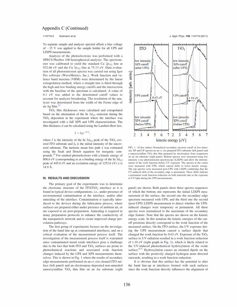
To separate sample and analyzer spectral offsets a bias voltage
of �15 V was applied to the sample holder for all UPS and
LIXPS measurements.
Analysis of the photoelectrons was performed with a
SPECS Phoibos 100 hemispherical analyzer. The spectrom-
eter was calibrated to yield the standard Cu 2p3/2 line at
932.66 eV and the Cu 3p3/2 line at 75.13 eV. Data evalua-
tion of all photoemission spectra was carried out using Igor
Pro software (WaveMetrics, Inc.). Work function and va-
lence band maxima (VBM) were determined by the linear
extrapolation method, where a straight line is fitted through
the high and low binding energy cutoffs and the intersection
with the baseline of the spectrum is calculated. A value of
0.1 eV was added to the determined cutoff values to
account for analyzer broadening. The resolution of the ana-
lyzer was determined from the width of the Fermi edge of
an Ag film.13
TiO2 film thicknesses were calculated and extrapolated
based on the attenuation of the In 3d5/2 emission during the
TiO2 deposition in the experiment where the interface was
investigated with a full XPS and UPS characterization. The
film thickness d can be calculated using the Lambert-Beer law,
I ¼ I0e�d=a;
where I is the intensity of the In 3d5/2 peak of the TiO2 cov-
ered ITO substrate and I0 is the initial intensity of the uncov-
ered substrate. The inelastic mean free path a was estimated
using the Seah and Dench equation for inorganic com-
pounds.14 For emitted photoelectrons with a kinetic energy of
808.6 eV (corresponding to at a binding energy of the In 3d5/2peak of 445.0 eV and an excitation energy of 1253.6 eV) a is
14.9 A.
III. RESULTS AND DISCUSSION
The primary goal of the experiments was to determine
the electronic structure of the ITO/TiO2 interface as it is
found in typical device configurations, i.e., under presence of
environmental contamination at the interface, and/or after
annealing of the interface. Contamination is typically intro-
duced to the devices during the fabrication process, where
surfaces are prepared either under presence of ambient air, or
are exposed to air post-preparation. Annealing is required in
many preparation protocols to enhance the conductivity of
the nanoparticle network and to create improved charge per-
colation pathways.
The first group of experiments focuses on the investiga-
tion of the band line-up at contaminated interfaces, and on a
critical evaluation of the measurement process itself. The
investigation of the measurement process itself is warranted
since contaminated metal oxide interfaces pose a challenge
due to the fact that both ITO and TiO2 surfaces are prone to
photochemical reactions and associated work function
changes induced by the UPS and XPS measurements them-
selves. This is shown in Fig. 1 where the results of secondary
edge measurements performed on an ex situ cleaned ITO sur-
face (left panel) and an electrospray-deposited non-annealed
nanocrystalline TiO2 thin film on an Au substrate (right
panel) are shown. Both panels show three spectra sequences
of which the bottom one represents the initial LIXPS mea-
surement of the surface, the second one the secondary edge
spectrum measured with UPS, and the third one the second
(post-UPS) LIXPS measurement to detect whether the UPS-
induced changes were temporary or permanent. All three
spectra were normalized to the maximum of the secondary
edge feature. Note that the spectra are shown on the kinetic
energy scale. In this notation the kinetic energies of the cut-
off positions directly correspond to the work function of the
measured surface. On the ITO surface, the UV exposure dur-
ing the UPS measurement caused a surface dipole that
changed the work function by 0.63 eV. Exposure of the TiO2
surface to UV radiation resulted in a work function reduction
of 1.10 eV (right graph in Fig. 1), which is likely related to
the UV-induced photochemical hydroxylation of the oxide
surface.6,11 Hydroxylation causes an oriented dipole on the
surface with the positively charged hydrogen atom directed
outwards, resulting in a work function reduction.
It is obvious that this artifact has the potential to alter
the band line-up at interfaces formed with such surfaces
since the work function directly influences the alignment of
FIG. 1. (Color online) Normalized secondary electron cutoff of low-inten-
sity XP and UP spectra on an ex situ prepared ITO substrate (left panel) and
a nanocrystalline TiO2 thin film prepared by electrospray from suspension
on an Au substrate (right panel). Bottom spectra were measured using low
intensity x-ray photoemission spectroscopy (LIXPS) and allow the determi-
nation of the work function before UV exposure. The spectra in the center
were measured with UPS, which caused shifts to lower kinetic energy.
The top spectra were measured post-UPS with LIXPS confirming that the
UV-induced shift of the secondary edge is permanent. These shifts indicate
a permanent work function reduction on both materials due to the exposure
to UV light during the UPS measurements.
113719-3 Gutmann et al. J. Appl. Phys. 109, 113719 (2011)
Downloaded 14 Jun 2011 to 134.106.136.73. Redistribution subject to AIP license or copyright; see http://jap.aip.org/about/rights_and_permissions
Appendix C (Continued)
136
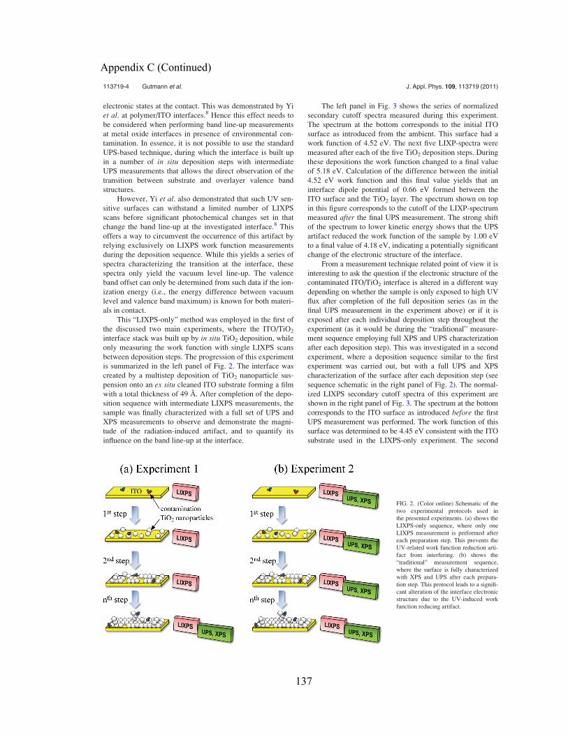
electronic states at the contact. This was demonstrated by Yi
et al. at polymer/ITO interfaces.8 Hence this effect needs to
be considered when performing band line-up measurements
at metal oxide interfaces in presence of environmental con-
tamination. In essence, it is not possible to use the standard
UPS-based technique, during which the interface is built up
in a number of in situ deposition steps with intermediate
UPS measurements that allows the direct observation of the
transition between substrate and overlayer valence band
structures.
However, Yi et al. also demonstrated that such UV sen-
sitive surfaces can withstand a limited number of LIXPS
scans before significant photochemical changes set in that
change the band line-up at the investigated interface.8 This
offers a way to circumvent the occurrence of this artifact by
relying exclusively on LIXPS work function measurements
during the deposition sequence. While this yields a series of
spectra characterizing the transition at the interface, these
spectra only yield the vacuum level line-up. The valence
band offset can only be determined from such data if the ion-
ization energy (i.e., the energy difference between vacuum
level and valence band maximum) is known for both materi-
als in contact.
This “LIXPS-only” method was employed in the first of
the discussed two main experiments, where the ITO/TiO2
interface stack was built up by in situ TiO2 deposition, while
only measuring the work function with single LIXPS scans
between deposition steps. The progression of this experiment
is summarized in the left panel of Fig. 2. The interface was
created by a multistep deposition of TiO2 nanoparticle sus-
pension onto an ex situ cleaned ITO substrate forming a film
with a total thickness of 49 A. After completion of the depo-
sition sequence with intermediate LIXPS measurements, the
sample was finally characterized with a full set of UPS and
XPS measurements to observe and demonstrate the magni-
tude of the radiation-induced artifact, and to quantify its
influence on the band line-up at the interface.
The left panel in Fig. 3 shows the series of normalized
secondary cutoff spectra measured during this experiment.
The spectrum at the bottom corresponds to the initial ITO
surface as introduced from the ambient. This surface had a
work function of 4.52 eV. The next five LIXP-spectra were
measured after each of the five TiO2 deposition steps. During
these depositions the work function changed to a final value
of 5.18 eV. Calculation of the difference between the initial
4.52 eV work function and this final value yields that an
interface dipole potential of 0.66 eV formed between the
ITO surface and the TiO2 layer. The spectrum shown on top
in this figure corresponds to the cutoff of the LIXP-spectrum
measured after the final UPS measurement. The strong shift
of the spectrum to lower kinetic energy shows that the UPS
artifact reduced the work function of the sample by 1.00 eV
to a final value of 4.18 eV, indicating a potentially significant
change of the electronic structure of the interface.
From a measurement technique related point of view it is
interesting to ask the question if the electronic structure of the
contaminated ITO/TiO2 interface is altered in a different way
depending on whether the sample is only exposed to high UV
flux after completion of the full deposition series (as in the
final UPS measurement in the experiment above) or if it is
exposed after each individual deposition step throughout the
experiment (as it would be during the “traditional” measure-
ment sequence employing full XPS and UPS characterization
after each deposition step). This was investigated in a second
experiment, where a deposition sequence similar to the first
experiment was carried out, but with a full UPS and XPS
characterization of the surface after each deposition step (see
sequence schematic in the right panel of Fig. 2). The normal-
ized LIXPS secondary cutoff spectra of this experiment are
shown in the right panel of Fig. 3. The spectrum at the bottom
corresponds to the ITO surface as introduced before the first
UPS measurement was performed. The work function of this
surface was determined to be 4.45 eV consistent with the ITO
substrate used in the LIXPS-only experiment. The second
FIG. 2. (Color online) Schematic of the
two experimental protocols used in
the presented experiments. (a) shows the
LIXPS-only sequence, where only one
LIXPS measurement is performed after
each preparation step. This prevents the
UV-related work function reduction arti-
fact from interfering. (b) shows the
“traditional” measurement sequence,
where the surface is fully characterized
with XPS and UPS after each prepara-
tion step. This protocol leads to a signifi-
cant alteration of the interface electronic
structure due to the UV-induced work
function reducing artifact.
113719-4 Gutmann et al. J. Appl. Phys. 109, 113719 (2011)
Downloaded 14 Jun 2011 to 134.106.136.73. Redistribution subject to AIP license or copyright; see http://jap.aip.org/about/rights_and_permissions
Appendix C (Continued)
137
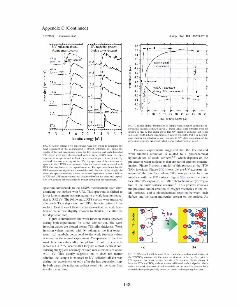
spectrum corresponds to the LIXPS measurement after char-acterizing the surface with UPS. This spectrum is shifted to
lower kinetic energy corresponding to a work function reduc-
tion to 3.92 eV. The following LIXPS spectra were measured
after each TiO2 deposition and UPS characterization of the
surface. Evaluation of these spectra shows that the work func-
tion of the surface slightly recovers to about 4.1 eV after the
last deposition step.
Figure 4 summarizes the work function trends observed
during both experiments for direct comparison. The work
function values are plotted versus TiO2 film thickness. Work
function values marked with (�) belong to the first experi-
ment. (h) symbols correspond to the work function values
obtained in the second experiment. Comparison of the final
work function values after completion of both experiments
(about 4.1–4.2 eV) reveals that they are almost identical con-
sidering the typical accuracy of such measurements of about
60.1 eV. This clearly suggests that it does not matter
whether the sample is exposed to UV radiation all the way
during the experiment or only after the last deposition step.
In both cases the radiation artifact results in the same final
interface condition.
Previous experiments suggested that the UV-induced
work function reduction is related to a photochemical
hydroxylation of oxide surfaces,6,11 which depends on the
presence of water molecules that are part of ambient contam-
ination. Figure 5 shows a model of this process at the ITO/
TiO2 interface. Figure 5(a) shows the pre-UV-exposure sit-
uation of the interface where TiO2 nanoparticles form an
interface with the ITO surface. Figure 5(b) shows the inter-
face after UV exposure, i.e., after photochemical hydroxyla-
tion of the oxide surface occurred.11 This process involves
the presence and/or creation of oxygen vacancies in the ox-
ide surfaces, and a photochemical reaction between such
defects and the water molecules present on the surface. As
FIG. 3. (Color online) Two experiments were performed to determine the
band alignment at the contaminated ITO/TiO2 interface. (a) shows the
results of the first experiment, where the ITO substrate and each deposited
TiO2 layer were only characterized with a single LIXPS scan, i.e., this
experiment was performed without UV exposure to prevent interference by
the work function reducing artifact. The top spectrum of this series corre-
sponds to the LIXPS scan measured after the sample was measured with
UPS after conclusion of the deposition series. This spectrum shows that the
UPS measurement significantly altered the work function of the sample. (b)
shows the spectra measured during the second experiment, where a full set
of XPS and UPS measurements was conducted before and after each deposi-
tion step, causing the work function artifact throughout the experiment.
FIG. 4. (Color online) Progression of sample work function during the ex-
perimental sequences shown in Fig. 2. These values were extracted from the
spectra in Fig. 3. The graph shows that UV radiation exposure led to the
same end result in both experiments. It can be concluded that it is insignifi-
cant whether the interface is only exposed to UV after completion of the
deposition sequence (�) or individually after each deposition step (h).
FIG. 5. (Color online) Schematic of the UV-induced surface modification at
the ITO/TiO2 interface. (a) illustrates the situation at the interface prior to
UV exposure. (b) shows the interface after UV exposure. Hydroxylation of
both the ITO and TiO2 surfaces causes additional surface dipoles, which
reduce the work functions of both materials. At the interface between both
materials the dipoles partially cancel out due to their opposing directions.
113719-5 Gutmann et al. J. Appl. Phys. 109, 113719 (2011)
Downloaded 14 Jun 2011 to 134.106.136.73. Redistribution subject to AIP license or copyright; see http://jap.aip.org/about/rights_and_permissions
Appendix C (Continued)
138
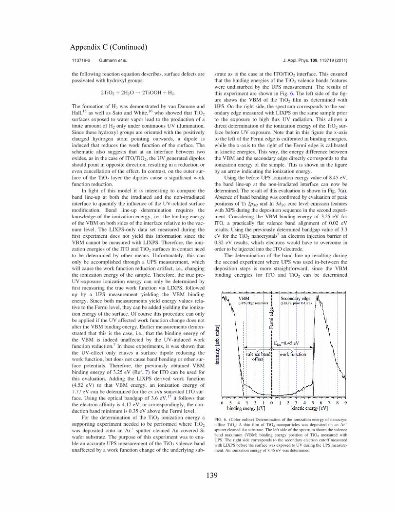
the following reaction equation describes, surface defects are
passivated with hydroxyl groups:
2TiO2 þ 2H2O ! 2TiOOHþ H2:
The formation of H2 was demonstrated by van Damme and
Hall,15 as well as Sato and White,16 who showed that TiO2
surfaces exposed to water vapor lead to the production of a
finite amount of H2 only under continuous UV illumination.
Since these hydroxyl groups are oriented with the positively
charged hydrogen atom pointing outwards, a dipole is
induced that reduces the work function of the surface. The
schematic also suggests that at an interface between two
oxides, as in the case of ITO/TiO2, the UV generated dipoles
should point in opposite direction, resulting in a reduction or
even cancellation of the effect. In contrast, on the outer sur-
face of the TiO2 layer the dipoles cause a significant work
function reduction.
In light of this model it is interesting to compare the
band line-up at both the irradiated and the non-irradiated
interface to quantify the influence of the UV-related surface
modification. Band line-up determination requires the
knowledge of the ionization energy, i.e., the binding energy
of the VBM on both sides of the interface relative to the vac-
uum level. The LIXPS-only data set measured during the
first experiment does not yield this information since the
VBM cannot be measured with LIXPS. Therefore, the ioni-
zation energies of the ITO and TiO2 surfaces in contact need
to be determined by other means. Unfortunately, this can
only be accomplished through a UPS measurement, which
will cause the work function reduction artifact, i.e., changing
the ionization energy of the sample. Therefore, the true pre-
UV-exposure ionization energy can only be determined by
first measuring the true work function via LIXPS, followed
up by a UPS measurement yielding the VBM binding
energy. Since both measurements yield energy values rela-
tive to the Fermi level, they can be added yielding the ioniza-
tion energy of the surface. Of course this procedure can only
be applied if the UV affected work function change does not
alter the VBM binding energy. Earlier measurements demon-
strated that this is the case, i.e., that the binding energy of
the VBM is indeed unaffected by the UV-induced work
function reduction.7 In these experiments, it was shown that
the UV-effect only causes a surface dipole reducing the
work function, but does not cause band bending or other sur-
face potentials. Therefore, the previously obtained VBM
binding energy of 3.25 eV (Ref. 7) for ITO can be used for
this evaluation. Adding the LIXPS derived work function
(4.52 eV) to that VBM energy, an ionization energy of
7.77 eV can be determined for the ex situ sonicated ITO sur-
face. Using the optical bandgap of 3.6 eV,17 it follows that
the electron affinity is 4.17 eV, or correspondingly, the con-
duction band minimum is 0.35 eV above the Fermi level.
For the determination of the TiO2 ionization energy a
supporting experiment needed to be performed where TiO2
was deposited onto an Arþ sputter cleaned Au covered Si
wafer substrate. The purpose of this experiment was to ena-
ble an accurate UPS measurement of the TiO2 valence band
unaffected by a work function change of the underlying sub-
strate as is the case at the ITO/TiO2 interface. This ensured
that the binding energies of the TiO2 valence bands features
were undisturbed by the UPS measurement. The results of
this experiment are shown in Fig. 6. The left side of the fig-
ure shows the VBM of the TiO2 film as determined with
UPS. On the right side, the spectrum corresponds to the sec-
ondary edge measured with LIXPS on the same sample prior
to the exposure to high flux UV radiation. This allows a
direct determination of the ionization energy of the TiO2 sur-
face before UV exposure. Note that in this figure the x-axis
to the left of the Fermi edge is calibrated in binding energies,
while the x-axis to the right of the Fermi edge is calibrated
in kinetic energies. This way, the energy difference between
the VBM and the secondary edge directly corresponds to the
ionization energy of the sample. This is shown in the figure
by an arrow indicating the ionization energy.
Using the before-UPS ionization energy value of 8.45 eV,
the band line-up at the non-irradiated interface can now be
determined. The result of this evaluation is shown in Fig. 7(a).
Absence of band bending was confirmed by evaluation of peak
positions of Ti 2p3/2 and In 3d3/2 core level emission features
with XPS during the deposition sequence in the second experi-
ment. Considering the VBM binding energy of 3.25 eV for
ITO, a practically flat valence band alignment of 0.02 eV
results. Using the previously determined bandgap value of 3.3
eV for the TiO2 nanocrystals5 an electron injection barrier of
0.32 eV results, which electrons would have to overcome in
order to be injected into the ITO electrode.
The determination of the band line-up resulting during
the second experiment where UPS was used in-between the
deposition steps is more straightforward, since the VBM
binding energies for ITO and TiO2 can be determined
FIG. 6. (Color online) Determination of the ionization energy of nanocrys-
talline TiO2: A thin film of TiO2 nanoparticles was deposited on an Arþ
sputter cleaned Au substrate. The left side of the spectrum shows the valence
band maximum (VBM) binding energy position of TiO2 measured with
UPS. The right side corresponds to the secondary electron cutoff measured
with LIXPS before the surface was exposed to UV during the UPS measure-
ment. An ionization energy of 8.45 eV was determined.
113719-6 Gutmann et al. J. Appl. Phys. 109, 113719 (2011)
Downloaded 14 Jun 2011 to 134.106.136.73. Redistribution subject to AIP license or copyright; see http://jap.aip.org/about/rights_and_permissions
Appendix C (Continued)
139
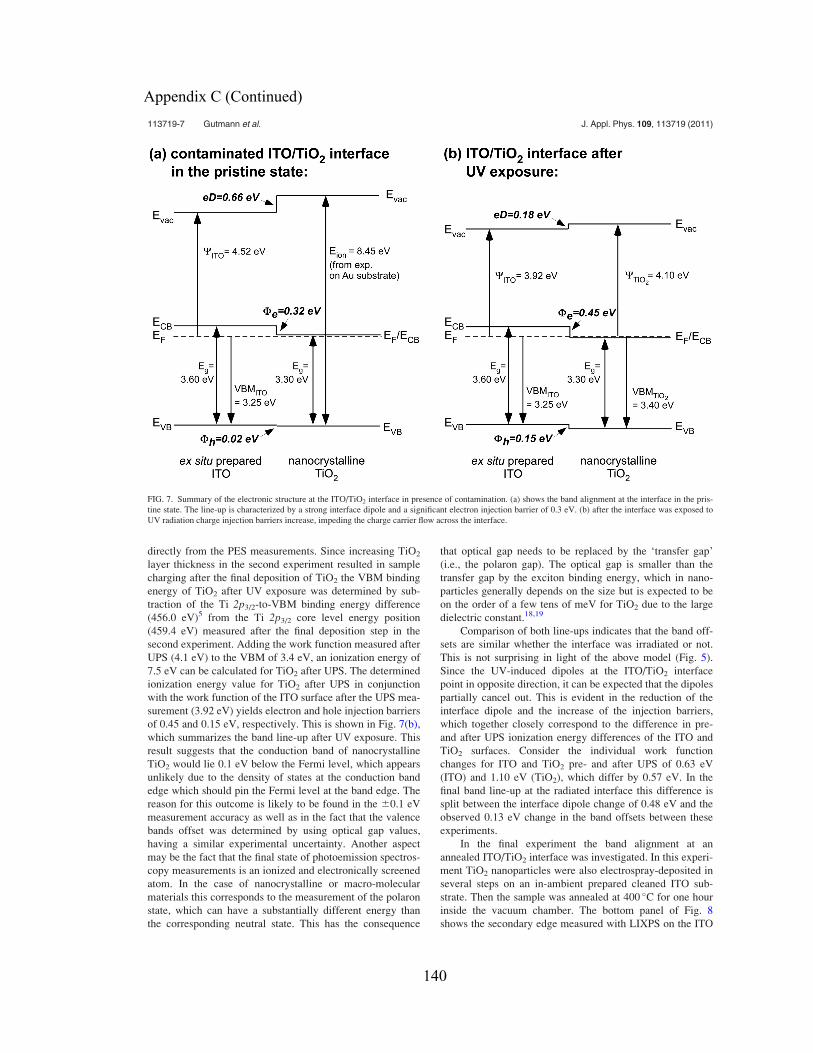
directly from the PES measurements. Since increasing TiO2
layer thickness in the second experiment resulted in sample
charging after the final deposition of TiO2 the VBM binding
energy of TiO2 after UV exposure was determined by sub-
traction of the Ti 2p3/2-to-VBM binding energy difference
(456.0 eV)5 from the Ti 2p3/2 core level energy position
(459.4 eV) measured after the final deposition step in the
second experiment. Adding the work function measured after
UPS (4.1 eV) to the VBM of 3.4 eV, an ionization energy of
7.5 eV can be calculated for TiO2 after UPS. The determined
ionization energy value for TiO2 after UPS in conjunction
with the work function of the ITO surface after the UPS mea-
surement (3.92 eV) yields electron and hole injection barriers
of 0.45 and 0.15 eV, respectively. This is shown in Fig. 7(b),
which summarizes the band line-up after UV exposure. This
result suggests that the conduction band of nanocrystalline
TiO2 would lie 0.1 eV below the Fermi level, which appears
unlikely due to the density of states at the conduction band
edge which should pin the Fermi level at the band edge. The
reason for this outcome is likely to be found in the 60.1 eV
measurement accuracy as well as in the fact that the valence
bands offset was determined by using optical gap values,
having a similar experimental uncertainty. Another aspect
may be the fact that the final state of photoemission spectros-
copy measurements is an ionized and electronically screened
atom. In the case of nanocrystalline or macro-molecular
materials this corresponds to the measurement of the polaron
state, which can have a substantially different energy than
the corresponding neutral state. This has the consequence
that optical gap needs to be replaced by the ‘transfer gap’
(i.e., the polaron gap). The optical gap is smaller than the
transfer gap by the exciton binding energy, which in nano-
particles generally depends on the size but is expected to be
on the order of a few tens of meV for TiO2 due to the large
dielectric constant.18,19
Comparison of both line-ups indicates that the band off-
sets are similar whether the interface was irradiated or not.
This is not surprising in light of the above model (Fig. 5).
Since the UV-induced dipoles at the ITO/TiO2 interface
point in opposite direction, it can be expected that the dipoles
partially cancel out. This is evident in the reduction of the
interface dipole and the increase of the injection barriers,
which together closely correspond to the difference in pre-
and after UPS ionization energy differences of the ITO and
TiO2 surfaces. Consider the individual work function
changes for ITO and TiO2 pre- and after UPS of 0.63 eV
(ITO) and 1.10 eV (TiO2), which differ by 0.57 eV. In the
final band line-up at the radiated interface this difference is
split between the interface dipole change of 0.48 eV and the
observed 0.13 eV change in the band offsets between these
experiments.
In the final experiment the band alignment at an
annealed ITO/TiO2 interface was investigated. In this experi-
ment TiO2 nanoparticles were also electrospray-deposited in
several steps on an in-ambient prepared cleaned ITO sub-
strate. Then the sample was annealed at 400 �C for one hour
inside the vacuum chamber. The bottom panel of Fig. 8
shows the secondary edge measured with LIXPS on the ITO
FIG. 7. Summary of the electronic structure at the ITO/TiO2 interface in presence of contamination. (a) shows the band alignment at the interface in the pris-
tine state. The line-up is characterized by a strong interface dipole and a significant electron injection barrier of 0.3 eV. (b) after the interface was exposed to
UV radiation charge injection barriers increase, impeding the charge carrier flow across the interface.
113719-7 Gutmann et al. J. Appl. Phys. 109, 113719 (2011)
Downloaded 14 Jun 2011 to 134.106.136.73. Redistribution subject to AIP license or copyright; see http://jap.aip.org/about/rights_and_permissions
Appendix C (Continued)
140
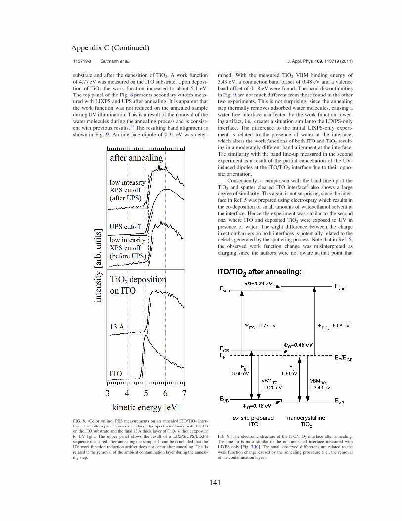
substrate and after the deposition of TiO2. A work function
of 4.77 eV was measured on the ITO substrate. Upon deposi-
tion of TiO2 the work function increased to about 5.1 eV.
The top panel of the Fig. 8 presents secondary cutoffs meas-
ured with LIXPS and UPS after annealing. It is apparent that
the work function was not reduced on the annealed sample
during UV illumination. This is a result of the removal of the
water molecules during the annealing process and is consist-
ent with previous results.11 The resulting band alignment is
shown in Fig. 9. An interface dipole of 0.31 eV was deter-
mined. With the measured TiO2 VBM binding energy of
3.43 eV, a conduction band offset of 0.48 eV and a valence
band offset of 0.18 eV were found. The band discontinuities
in Fig. 9 are not much different from those found in the other
two experiments. This is not surprising, since the annealing
step thermally removes adsorbed water molecules, causing a
water-free interface unaffected by the work function lower-
ing artifact, i.e., creates a situation similar to the LIXPS-only
interface. The difference to the initial LIXPS-only experi-
ment is related to the presence of water at the interface,
which alters the work functions of both ITO and TiO2 result-
ing in a moderately different band alignment at the interface.
The similarity with the band line-up measured in the second
experiment is a result of the partial cancellation of the UV-
induced dipoles at the ITO/TiO2 interface due to their oppo-
site orientation.
Consequently, a comparison with the band line-up at the
TiO2 and sputter cleaned ITO interface5 also shows a large
degree of similarity. This again is not surprising, since the inter-
face in Ref. 5 was prepared using electrospray which results in
the co-deposition of small amounts of water/ethanol solvent at
the interface. Hence the experiment was similar to the second
one, where ITO and deposited TiO2 were exposed to UV in
presence of water. The slight difference between the charge
injection barriers on both interfaces is potentially related to the
defects generated by the sputtering process. Note that in Ref. 5,
the observed work function change was misinterpreted as
charging since the authors were not aware at that point that
FIG. 8. (Color online) PES measurements on an annealed ITO/TiO2 inter-
face: The bottom panel shows secondary edge spectra measured with LIXPS
on the ITO substrate and the final 13 A thick layer of TiO2 without exposure
to UV light. The upper panel shows the result of a LIXPS/UPS/LIXPS
sequence measured after annealing the sample. It can be concluded that the
UV work function reduction artifact does not occur after annealing. This is
related to the removal of the ambient contamination layer during the anneal-
ing step.
FIG. 9. The electronic structure of the ITO/TiO2 interface after annealing.
The line-up is most similar to the non-annealed interface measured with
LIXPS only [Fig. 7(b)]. The small observed differences are related to the
work function change caused by the annealing procedure (i.e., the removal
of the contamination layer).
113719-8 Gutmann et al. J. Appl. Phys. 109, 113719 (2011)
Downloaded 14 Jun 2011 to 134.106.136.73. Redistribution subject to AIP license or copyright; see http://jap.aip.org/about/rights_and_permissions
Appendix C (Continued)
141
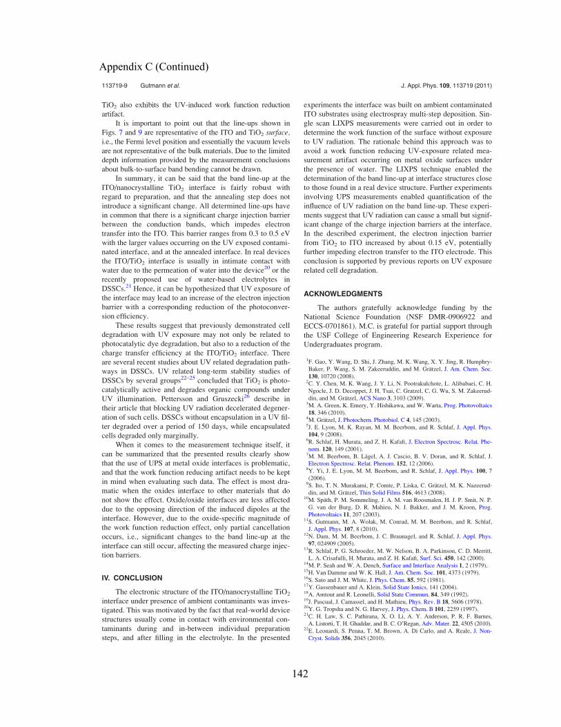
TiO2 also exhibits the UV-induced work function reduction
artifact.
It is important to point out that the line-ups shown in
Figs. 7 and 9 are representative of the ITO and TiO2 surface,i.e., the Fermi level position and essentially the vacuum levels
are not representative of the bulk materials. Due to the limited
depth information provided by the measurement conclusions
about bulk-to-surface band bending cannot be drawn.
In summary, it can be said that the band line-up at the
ITO/nanocrystalline TiO2 interface is fairly robust with
regard to preparation, and that the annealing step does not
introduce a significant change. All determined line-ups have
in common that there is a significant charge injection barrier
between the conduction bands, which impedes electron
transfer into the ITO. This barrier ranges from 0.3 to 0.5 eV
with the larger values occurring on the UV exposed contami-
nated interface, and at the annealed interface. In real devices
the ITO/TiO2 interface is usually in intimate contact with
water due to the permeation of water into the device20 or the
recently proposed use of water-based electrolytes in
DSSCs.21 Hence, it can be hypothesized that UV exposure of
the interface may lead to an increase of the electron injection
barrier with a corresponding reduction of the photoconver-
sion efficiency.
These results suggest that previously demonstrated cell
degradation with UV exposure may not only be related to
photocatalytic dye degradation, but also to a reduction of the
charge transfer efficiency at the ITO/TiO2 interface. There
are several recent studies about UV related degradation path-
ways in DSSCs. UV related long-term stability studies of
DSSCs by several groups22–25 concluded that TiO2 is photo-
catalytically active and degrades organic compounds under
UV illumination. Pettersson and Gruszecki26 describe in
their article that blocking UV radiation decelerated degener-
ation of such cells. DSSCs without encapsulation in a UV fil-
ter degraded over a period of 150 days, while encapsulated
cells degraded only marginally.
When it comes to the measurement technique itself, it
can be summarized that the presented results clearly show
that the use of UPS at metal oxide interfaces is problematic,
and that the work function reducing artifact needs to be kept
in mind when evaluating such data. The effect is most dra-
matic when the oxides interface to other materials that do
not show the effect. Oxide/oxide interfaces are less affected
due to the opposing direction of the induced dipoles at the
interface. However, due to the oxide-specific magnitude of
the work function reduction effect, only partial cancellation
occurs, i.e., significant changes to the band line-up at the
interface can still occur, affecting the measured charge injec-
tion barriers.
IV. CONCLUSION
The electronic structure of the ITO/nanocrystalline TiO2
interface under presence of ambient contaminants was inves-
tigated. This was motivated by the fact that real-world device
structures usually come in contact with environmental con-
taminants during and in-between individual preparation
steps, and after filling in the electrolyte. In the presented
experiments the interface was built on ambient contaminated
ITO substrates using electrospray multi-step deposition. Sin-
gle scan LIXPS measurements were carried out in order to
determine the work function of the surface without exposure
to UV radiation. The rationale behind this approach was to
avoid a work function reducing UV-exposure related mea-
surement artifact occurring on metal oxide surfaces under
the presence of water. The LIXPS technique enabled the
determination of the band line-up at interface structures close
to those found in a real device structure. Further experiments
involving UPS measurements enabled quantification of the
influence of UV radiation on the band line-up. These experi-
ments suggest that UV radiation can cause a small but signif-
icant change of the charge injection barriers at the interface.
In the described experiment, the electron injection barrier
from TiO2 to ITO increased by about 0.15 eV, potentially
further impeding electron transfer to the ITO electrode. This
conclusion is supported by previous reports on UV exposure
related cell degradation.
ACKNOWLEDGMENTS
The authors gratefully acknowledge funding by the
National Science Foundation (NSF DMR-0906922 and
ECCS-0701861). M.C. is grateful for partial support through
the USF College of Engineering Research Experience for
Undergraduates program.
1F. Gao, Y. Wang, D. Shi, J. Zhang, M. K. Wang, X. Y. Jing, R. Humphry-
Baker, P. Wang, S. M. Zakeeruddin, and M. Gratzel, J. Am. Chem. Soc.
130, 10720 (2008).2C. Y. Chen, M. K. Wang, J. Y. Li, N. Pootrakulchote, L. Alibabaei, C. H.
Ngocle, J. D. Decoppet, J. H. Tsai, C. Gratzel, C. G. Wu, S. M. Zakeerud-
din, and M. Gratzel, ACS Nano 3, 3103 (2009).3M. A. Green, K. Emery, Y. Hishikawa, and W. Warta, Prog. Photovoltaics
18, 346 (2010).4M. Gratzel, J. Photochem. Photobiol. C 4, 145 (2003).5J. E. Lyon, M. K. Rayan, M. M. Beerbom, and R. Schlaf, J. Appl. Phys.
104, 9 (2008).6R. Schlaf, H. Murata, and Z. H. Kafafi, J. Electron Spectrosc. Relat. Phe-
nom. 120, 149 (2001).7M. M. Beerbom, B. Lagel, A. J. Cascio, B. V. Doran, and R. Schlaf, J.
Electron Spectrosc. Relat. Phenom. 152, 12 (2006).8Y. Yi, J. E. Lyon, M. M. Beerbom, and R. Schlaf, J. Appl. Phys. 100, 7(2006).
9S. Ito, T. N. Murakami, P. Comte, P. Liska, C. Gratzel, M. K. Nazeerud-
din, and M. Gratzel, Thin Solid Films 516, 4613 (2008).10M. Spath, P. M. Sommeling, J. A. M. van Roosmalen, H. J. P. Smit, N. P.
G. van der Burg, D. R. Mahieu, N. J. Bakker, and J. M. Kroon, Prog.
Photovoltaics 11, 207 (2003).11S. Gutmann, M. A. Wolak, M. Conrad, M. M. Beerbom, and R. Schlaf,
J. Appl. Phys. 107, 8 (2010).12N. Dam, M. M. Beerbom, J. C. Braunagel, and R. Schlaf, J. Appl. Phys.
97, 024909 (2005).13R. Schlaf, P. G. Schroeder, M. W. Nelson, B. A. Parkinson, C. D. Merritt,
L. A. Crisafulli, H. Murata, and Z. H. Kafafi, Surf. Sci. 450, 142 (2000).14M. P. Seah and W. A. Dench, Surface and Interface Analysis 1, 2 (1979).15H. Van Damme and W. K. Hall, J. Am. Chem. Soc. 101, 4373 (1979).16S. Sato and J. M. White, J. Phys. Chem. 85, 592 (1981).17Y. Gassenbauer and A. Klein, Solid State Ionics, 141 (2004).18A. Amtout and R. Leonelli, Solid State Commun. 84, 349 (1992).19J. Pascual, J. Camassel, and H. Mathieu, Phys. Rev. B 18, 5606 (1978).20Y. G. Tropsha and N. G. Harvey, J. Phys. Chem. B 101, 2259 (1997).21C. H. Law, S. C. Pathirana, X. O. Li, A. Y. Anderson, P. R. F. Barnes,
A. Listorti, T. H. Ghaddar, and B. C. O’Regan, Adv. Mater. 22, 4505 (2010).22E. Leonardi, S. Penna, T. M. Brown, A. Di Carlo, and A. Reale, J. Non-
Cryst. Solids 356, 2045 (2010).
113719-9 Gutmann et al. J. Appl. Phys. 109, 113719 (2011)
Downloaded 14 Jun 2011 to 134.106.136.73. Redistribution subject to AIP license or copyright; see http://jap.aip.org/about/rights_and_permissions
Appendix C (Continued)
142

23A. Hinsch, J. M. Kroon, R. Kern, I. Uhlendorf, J. Holzbock, A. Meyer, and
J. Ferber, Prog. Photovoltaics 9, 425 (2001).24P. M. Sommeling, M. Spath, H. J. P. Smit, N. J. Bakker, and J. M. Kroon,
J. Photochem. Photobiol. A 164, 137 (2004).
25A. Fujishima, T. N. Rao, and D. A. Tryk, J. Photochem. Photobiol. C 1, 1(2000).
26H. Pettersson and T. Gruszecki, Sol. Energ. Mat. Sol. C 70, 203
(2001).
113719-10 Gutmann et al. J. Appl. Phys. 109, 113719 (2011)
Downloaded 14 Jun 2011 to 134.106.136.73. Redistribution subject to AIP license or copyright; see http://jap.aip.org/about/rights_and_permissions
Appendix C (Continued)
143
ABOUT THE AUTHOR
Sebastian Gutmann was born in on October 8, 1981 in Meiningen, Germany and
earned a Diploma degree in Chemistry from Carl-von-Ossietzky University of Oldenburg,
Germany in 2007. In 2005 he received funding by the German Academic Exchange
Foundation (DAAD) to study at Southeast University in Nanjing, China and in 2007 he
worked on his diploma project in thermodynamics at Nanjing University of Technology,
China under supervision of Professor Dr. Jürgen Gmehling and Professor Dr. Xiaohua Lu.
This visit was funded by the Ernest Solvay Foundation of Germany. He continued his
education under supervision of Professor Dr. Rudy Schlaf at the University of South
Florida, where he worked on photoemission spectroscopy investigations of electronic
materials. Between 2008 and 2011 he instructed General Chemistry laboratory courses at
the Department of Chemistry. In summer of 2011 he was a recipient of the Brighthouse
endowed fellowship, which supported the preparation of his dissertation.
Sebastian Gutmann gave oral presentations and poster presentations at the
American Vacuum Society symposia in San Jose, CA (2009) and Albuquerque, NM
(2010) and contributed to more than ten peer-reviewed publications.