Embed Size (px)
Citation preview
1
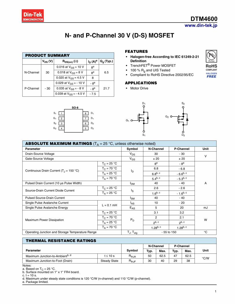
N- and P-Channel 30 V (D-S) MOSFET
FEATURES• Halogen-free According to IEC 61249-2-21
Definition• TrenchFET® Power MOSFET• 100 % Rg and UIS Tested• Compliant to RoHS Directive 2002/95/EC
APPLICATIONS• Motor Drive
Notes: a. Based on TC = 25 °C.b. Surface mounted on 1" x 1" FR4 board.c. t = 10 s.d. Maximum under steady state conditions is 120 °C/W (n-channel) and 110 °C/W (p-channel).e. Package limited.
PRODUCT SUMMARY VDS (V) RDS(on) (Ω) ID (A)a Qg (Typ.)
N-Channel 30
0.016 at VGS = 10 V 8e
6.50.018 at VGS = 8 V 8e
0.020 at VGS = 4.5 V 8
P-Channel - 30
0.029 at VGS = - 10 V - 8e
21.70.035 at VGS = - 8 V - 8e
0.039 at VGS = - 4.5 V - 7.5
S1 D1
G1 D1
S2 D2
G2 D2
SO-8
5
6
7
8
2
3
4
1
D1
G1
S1
S2
G2
D2
ABSOLUTE MAXIMUM RATINGS (TA = 25 °C, unless otherwise noted)Parameter Symbol N-Channel P-Channel Unit
Drain-Source Voltage VDS 30 - 30V
Gate-Source Voltage VGS ± 20 ± 20
Continuous Drain Current (TJ = 150 °C)
TC = 25 °C
ID
8e - 8e
A
TC = 70 °C 6.8 - 6.8
TA = 25 °C 6.8b, c - 6.6b, c
TA = 70 °C 5.4b, c - 5.3b, c
Pulsed Drain Current (10 µs Pulse Width) IDM 40 - 40
Source-Drain Current Diode CurrentTC = 25 °C
IS2.6 - 2.6
TA = 25 °C 1.6b, c - 1.6b, c
Pulsed Source-Drain Current ISM 40 - 40
Single Pulse Avalanche CurrentL = 0.1 mH
IAS 10 - 20
Single Pulse Avalanche Energy EAS 5 20 mJ
Maximum Power Dissipation
TC = 25 °C
PD
3.1 3.2
WTC = 70 °C 2 2.1
TA = 25 °C 2b, c 2b, c
TA = 70 °C 1.28b, c 1.28b, c
Operating Junction and Storage Temperature Range TJ, Tstg - 55 to 150 °C
THERMAL RESISTANCE RATINGS
Parameter Symbol N-Channel P-Channel
Unit Typ. Max. Typ. Max.
Maximum Junction-to-Ambientb, d t ≤ 10 s RthJA 50 62.5 47 62.5°C/W
Maximum Junction-to-Foot (Drain) Steady State RthJF 30 40 29 38
www.din-tek.jp DTM4600
2
SPECIFICATIONS (TJ = 25 °C, unless otherwise noted)Parameter Symbol Test Conditions Min. Typ.a Max. Unit
Static
Drain-Source Breakdown Voltage VDSVGS = 0 V, ID = 250 µA N-Ch 30
VVGS = 0 V, ID = - 250 µA P-Ch - 30
VDS Temperature Coefficient ΔVDS/TJID = 250 µA N-Ch 30
mV/°CID = - 250 µA P-Ch - 24
VGS(th) Temperature Coefficient ΔVGS(th)/TJID = 250 µA N-Ch - 4.1
ID = - 250 µA P-Ch 5
Gate Threshold Voltage VGS(th) VDS = VGS, ID = 250 µA N-Ch 1 2.2
VVDS = VGS, ID = - 250 µA P-Ch - 1.2 - 2.5
Gate-Body Leakage IGSSVDS = 0 V, VGS = ± 20 V N-Ch ± 100
nAVDS = 0 V, VGS = ± 20 V P-Ch ± 100
Zero Gate Voltage Drain Current IDSS
VDS = 30 V, VGS = 0 V N-Ch 1
µAVDS = - 30 V, VGS = 0 V P-Ch - 1
VDS = 30 V, VGS = 0 V, TJ = 55 °C N-Ch 10
VDS = - 30 V, VGS = 0 V, TJ = 55 °C P-Ch - 10
On-State Drain Currentb ID(on) VDS = 5 V, VGS = 10 V N-Ch 20
AVDS = - 5 V, VGS = - 10 V P-Ch - 20
Drain-Source On-State Resistanceb RDS(on)
VGS = 10 V, ID = 6.8 A N-Ch 0.016
Ω
VGS = - 10 V, ID = - 8 A P-Ch 0.029
VGS = 8 V, ID = 6.7 A N-Ch 0.018
VGS = - 8 V, ID = - 6.5 A P-Ch 0.035
VGS = 4.5 V, ID = 6.6 A N-Ch 0.020
VGS = - 4.5 V, ID = - 5 A P-Ch 0.039
Forward Transconductanceb gfsVDS = 15 V, ID = 6.8 A N-Ch 27
SVDS = - 15 V, ID = - 6.7 A P-Ch 25
Dynamica
Input Capacitance Ciss N-ChannelVDS = 20 V, VGS = 0 V, f = 1 MHz
P-ChannelVDS = - 20 V, VGS = 0 V, f = 1 MHz
N-Ch 600
pF
P-Ch 1010
Output Capacitance CossN-Ch 115
P-Ch 240
Reverse Transfer Capacitance Crss N-Ch 41
P-Ch 202
Total Gate Charge Qg
VDS = 20 V, VGS = 10 V, ID = 7 A N-Ch 13.3 20
nC
VDS = - 20 V, VGS = - 10 V, ID = - 7 A P-Ch 41.5 63
N-ChannelVDS = 20 V, VGS = 4.5 V, ID = 7 A
P-ChannelVDS = - 20 V, VGS = - 4.5 V, ID = - 7 A
N-Ch 6.5 10
P-Ch 21.7 33
Gate-Source Charge Qgs N-Ch 2.3
P-Ch 5.6
Gate-Drain Charge Qgd N-Ch 1.7
P-Ch 9.8
Gate Resistance Rg f = 1 MHzN-Ch 0.3 1.3 2.6
ΩP-Ch 1.3 6.4 12.8
www.din-tek.jp DTM4600
0.018
0.032
0.020
0.039
0.022
0.043

3
Notes:a. Guaranteed by design, not subject to production testing.b. Pulse test; pulse width ≤ 300 µs, duty cycle ≤ 2 %.
Stresses beyond those listed under “Absolute Maximum Ratings” may cause permanent damage to the device. These are stress ratings only, and functional operationof the device at these or any other conditions beyond those indicated in the operational sections of the specifications is not implied. Exposure to absolute maximumrating conditions for extended periods may affect device reliability.
SPECIFICATIONS (TJ = 25 °C, unless otherwise noted)
Parameter Symbol Test Conditions Min. Typ.a Max. Unit
Dynamica
Turn-On Delay Time td(on) N-ChannelVDD = 20 V, RL = 3.7 Ω
ID ≅ 5.4 A, VGEN = 10 V, Rg = 1 Ω
P-ChannelVDD = - 20 V, RL = 2 Ω
ID ≅ - 7 A, V GEN = - 10 V, Rg = 1 Ω
N-Ch 5 10
ns
P-Ch 10 20
Rise Time trN-Ch 10 20
P-Ch 9 18
Turn-Off Delay Time td(off) N-Ch 16 25
P-Ch 50 90
Fall Time tfN-Ch 7 14
P-Ch 13 26
Turn-On Delay Time td(on) N-ChannelVDD = 20 V, RL = 3.7 Ω
ID ≅ 5.4 A, VGEN = 4.5 V, Rg = 1 Ω
P-ChannelVDD = - 20 V, RL = 2 Ω
ID ≅ - 7 A, VGEN = - 4.5 V, Rg = 1 Ω
N-Ch 11 22
P-Ch 42 75
Rise Time trN-Ch 12 22
P-Ch 40 70
Turn-Off Delay Time td(off) N-Ch 17 26
P-Ch 40 70
Fall Time tfN-Ch 7 14
P-Ch 18 35
Drain-Source Body Diode Characteristics
Continuous Source-Drain Diode Current IS TC = 25 °C N-Ch 2.6
AP-Ch - 2.6
Pulse Diode Forward Currenta ISMN-Ch 40
P-Ch - 40
Body Diode Voltage VSDIS = 5.4 A N-Ch 0.81 1.2
VIS = - 2 A P-Ch - 0.77 - 1.2
Body Diode Reverse Recovery Time trr
N-ChannelIF = 5 A, dI/dt = 100 A/µs, TJ = 25 °C
P-Channel IF = - 5 A, dI/dt = - 100 A/µs, TJ = 25 °C
N-Ch 17 34ns
P-Ch 41 80
Body Diode Reverse Recovery Charge QrrN-Ch 10 20
nCP-Ch 32 65
Reverse Recovery Fall Time taN-Ch 10
nsP-Ch 15
Reverse Recovery Rise Time tbN-Ch 7
P-Ch 26
www.din-tek.jp DTM4600
4
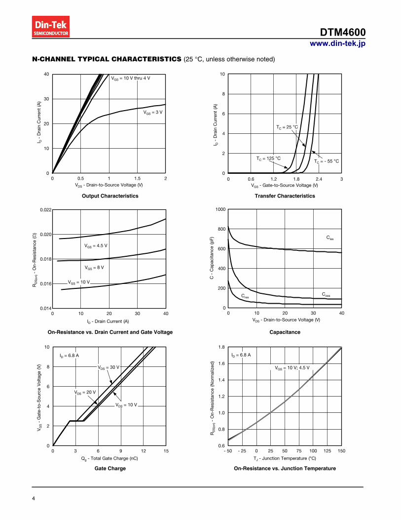
N-CHANNEL TYPICAL CHARACTERISTICS (25 °C, unless otherwise noted)
Output Characteristics
On-Resistance vs. Drain Current and Gate Voltage
Gate Charge
0
10
20
30
40
0 0.5 1 1.5 2
I D -
Dra
in C
urre
nt (
A)
VDS - Drain-to-Source Voltage (V)
VGS = 10 V thru 4 V
VGS = 3 V
0.014
0.016
0.018
0.020
0.022
0 10 20 30 40
RD
S(o
n) -
On-
Res
ista
nce
(Ω)
ID - Drain Current (A)
VGS = 8 V
VGS = 4.5 V
VGS = 10 V
0
2
4
6
8
10
0 3 6 9 12 15
VG
S -
Gat
e-to
-Sou
rce
Vol
tage
(V)
Qg - Total Gate Charge (nC)
VDS = 10 V
VDS = 20 V
VDS = 30 V
ID = 6.8 A
Transfer Characteristics
Capacitance
On-Resistance vs. Junction Temperature
0
2
4
6
8
10
0 0.6 1.2 1.8 2.4 3
I D -
Dra
in C
urre
nt (
A)
VGS - Gate-to-Source Voltage (V)
TC = 25 °C
TC = 125 °C TC = - 55 °C
0
200
400
600
800
1000
0 10 20 30 40
C -
Cap
acita
nce
(pF)
VDS - Drain-to-Source Voltage (V)
Ciss
Coss Crss
0.6
0.8
1.0
1.2
1.4
1.6
1.8
- 50 - 25 0 25 50 75 100 125 150
RD
S(o
n) -
On-
Res
ista
nce
(Nor
mal
ized
)
TJ - Junction Temperature (°C)
ID = 6.8 A
VGS = 10 V; 4.5 V
www.din-tek.jp DTM4600
5
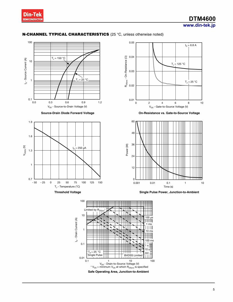
N-CHANNEL TYPICAL CHARACTERISTICS (25 °C, unless otherwise noted)
Source-Drain Diode Forward Voltage
Threshold Voltage
0.1
1
10
100
0.0 0.3 0.6 0.9 1.2
I S -
Sou
rce
Cur
rent
(A
)
VSD - Source-to-Drain Voltage (V)
TJ = 150 °C
TJ = 25 °C
0.7
1
1.3
1.6
1.9
- 50 - 25 0 5025 75 100 125 150
VG
S(th
) (V
)
TJ - Temperature (°C)
ID = 250 μA
On-Resistance vs. Gate-to-Source Voltage
Single Pulse Power, Junction-to-Ambient
0.01
0.02
0.03
0.04
0.05
0 2 4 6 8 10
RD
S(o
n) -
On-
Res
ista
nce
(Ω)
VGS - Gate-to-Source Voltage (V)
TJ = 125 °C
TJ = 25 °C
ID = 6.8 A
0
12
24
36
48
60
011100.0 0.01Time (s)
Pow
er (W
)
0.1
Safe Operating Area, Junction-to-Ambient
0.01
0.1
1
10
100
0.1 1 10 100
I D -
Dra
in C
urre
nt (
A)
VDS - Drain-to-Source Voltage (V) * VGS > minimum VGS at which RDS(on) is specified
100 ms
Limited by RDS(on)*
1 ms
TA = 25 °C Single Pulse BVDSS Limited
10 ms
100 μs
1 s
DC 10 s
www.din-tek.jp DTM4600

6
N-CHANNEL TYPICAL CHARACTERISTICS (25 °C, unless otherwise noted)
* The power dissipation PD is based on TJ(max) = 150 °C, using junction-to-case thermal resistance, and is more useful in settling the upper
dissipation limit for cases where additional heatsinking is used. It is used to determine the current rating, when this rating falls below the package
limit.
Current Derating*
0
2
4
6
8
10
0 25 50 75 100 125 150
I D -
Dra
in C
urre
nt (
A)
TC - Case Temperature (°C)
Power Derating, Junction-to-Foot
0
1
2
3
4
0 25 50 75 100 125 150
Pow
er (W
)
TC - Case Temperature (°C)
Power Derating, Junction-to-Ambient
0.0
0.25
0.50
0.75
1.0
1.25
0 25 50 75 100 125 150
Pow
er (W
)
TA - Ambient Temperature (°C)
www.din-tek.jp DTM4600
7
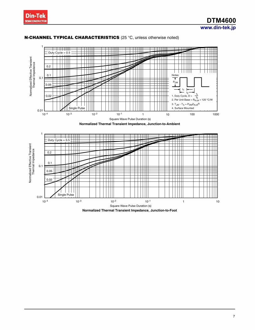
N-CHANNEL TYPICAL CHARACTERISTICS (25 °C, unless otherwise noted)
Normalized Thermal Transient Impedance, Junction-to-Ambient
10-3 10-2 1 10 100010-110-4 100
0.2
0.1
Square Wave Pulse Duration (s)
Nor
mal
ized
Effe
ctiv
eTr
ansi
ent
Ther
mal
Imp
edan
ce
1
0.1
0.01
t1t2
Notes:
PDM
1. Duty Cycle, D =
2. Per Unit Base = RthJA = 120 °C/W
3. TJM - TA = PDMZthJA(t)
t1t2
4. Surface Mounted
Duty Cycle = 0.5
Single Pulse
0.02
0.05
Normalized Thermal Transient Impedance, Junction-to-Foot
10-3 10-2 01110-110-4
0.2
0.1
Duty Cycle = 0.5
Square Wave Pulse Duration (s)
Nor
mal
ized
Effe
ctiv
eTr
ansi
ent
Ther
mal
Imp
edan
ce
1
0.1
0.01
0.05
Single Pulse
0.02
www.din-tek.jp DTM4600
8
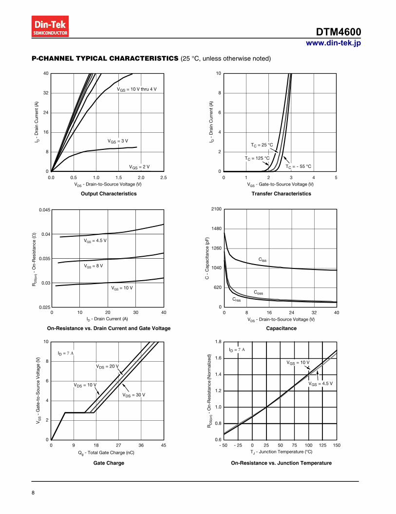
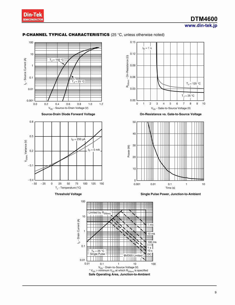
P-CHANNEL TYPICAL CHARACTERISTICS (25 °C, unless otherwise noted)
Output Characteristics
On-Resistance vs. Drain Current and Gate Voltage
Gate Charge
0
8
16
24
32
40
0.0 0.5 1.0 1.5 2.0 2.5
VGS = 10 V thru 4 V
VGS = 3 V
VGS = 2 V
VDS - Drain-to-Source Voltage (V)
I D -
Dra
in C
urre
nt (A
)
0.025
0.03
0.035
0.04
0.045
0 10 20 30 40
RD
S(o
n) -
On-
Res
ista
nce
(Ω)
ID - Drain Current (A)
VGS = 8 V
VGS = 4.5 V
VGS = 10 V
0
2
4
6
8
10
0 9 18 27 36 45
ID = 7 A
VDS = 20 V
VDS = 30 V
VDS = 10 V
Qg - Total Gate Charge (nC)
VG
S -
Gat
e-to
-Sou
rce
Vol
tage
(V)
Transfer Characteristics
Capacitance
On-Resistance vs. Junction Temperature
0
2
4
6
8
10
0 1 2 3 4 5
TC = 125 °C
TC = 25 °C
TC = - 55 °C
VGS - Gate-to-Source Voltage (V)
I D -
Dra
in C
urre
nt (A
)
Crss
0
620
1040
1260
1480
2100
0 8 16 24 32 40
Ciss
Coss
VDS - Drain-to-Source Voltage (V)
C -
Cap
acita
nce
(pF)
0.6
0.8
1.0
1.2
1.4
1.6
1.8
- 50 - 25 0 25 50 75 100 125 150
ID = 7 A
VGS = 4.5 V
VGS = 10 V
TJ - Junction Temperature (°C)
(Nor
mal
ized
)R
DS
(on)
- O
n-R
esis
tanc
e
www.din-tek.jp DTM4600
9
P-CHANNEL TYPICAL CHARACTERISTICS (25 °C, unless otherwise noted)
Source-Drain Diode Forward Voltage
Threshold Voltage
0.0 0.2 0.4 0.6 0.8 1.0 1.2
1
0.01
0.001
0.1
10
100
TJ = 25 °C
TJ = 150 °C
VSD - Source-to-Drain Voltage (V)
I S -
Sou
rce
Cur
rent
(A)
- 0.4
- 0.1
0.2
0.5
0.8
- 50 - 25 0 25 50 75 100 125 150
ID = 5 mA
ID = 250 μA
VG
S(th
) Var
ianc
e (V
)
TJ - Temperature (°C)
On-Resistance vs. Gate-to-Source Voltage
Single Pulse Power, Junction-to-Ambient
0.00
0.03
0.06
0.09
0.12
0.15
0 1 2 3 4 5 6 7 8 9 10
TJ = 25 °C
TJ = 125 °C
ID = 7 A
RD
S(o
n) -
On-
Res
ista
nce
(Ω)
VGS - Gate-to-Source Voltage (V)
0
10
20
30
40
50
011100.0 0.01 0.1Time (s)
Pow
er (W
)
Safe Operating Area, Junction-to-Ambient
0.01
100
1
100
0.01
0.1
10 s
10 ms
0.1 1 10
10
TA = 25 °CSingle Pulse
1 ms
DCBVDSS Limited
1 s
100 ms
Limited by RDS(on)*
VDS - Drain-to-Source Voltage (V)* VGS > minimum VGS at which RDS(on) is specified
I D -
Dra
in C
urre
nt (A
)
www.din-tek.jp DTM4600
10
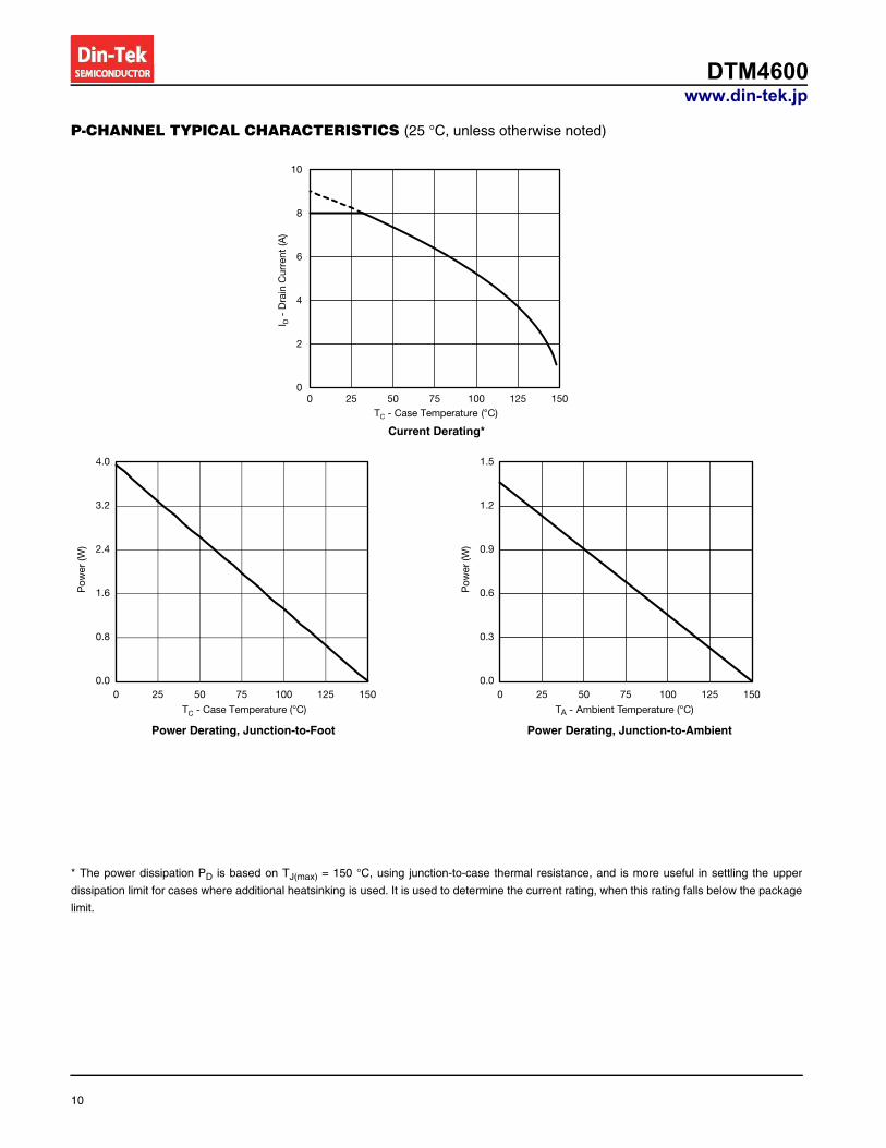
P-CHANNEL TYPICAL CHARACTERISTICS (25 °C, unless otherwise noted)
* The power dissipation PD is based on TJ(max) = 150 °C, using junction-to-case thermal resistance, and is more useful in settling the upper
dissipation limit for cases where additional heatsinking is used. It is used to determine the current rating, when this rating falls below the package
limit.
Current Derating*
0
2
4
6
8
10
0 25 50 75 100 125 150
I D -
Dra
in C
urre
nt (
A)
TC - Case Temperature (°C)
Power Derating, Junction-to-Foot
0.0
0.8
1.6
2.4
3.2
4.0
0 25 50 75 100 125 150
TC - Case Temperature (°C)
Pow
er (W
)
Power Derating, Junction-to-Ambient
0.0
0.3
0.6
0.9
1.2
1.5
0 25 50 75 100 125 150
TA - Ambient Temperature (°C)
Pow
er(W
)
www.din-tek.jp DTM4600
11
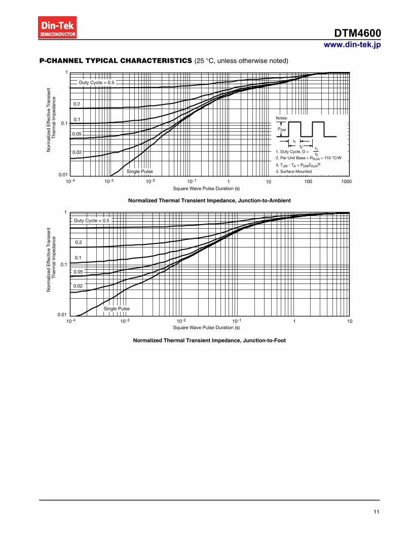
P-CHANNEL TYPICAL CHARACTERISTICS (25 °C, unless otherwise noted)
Normalized Thermal Transient Impedance, Junction-to-Ambient
10-3 10-2 1 10 100010-110-4 100
0.2
0.1
Square Wave Pulse Duration (s)
Nor
mal
ized
Effe
ctiv
eTr
ansi
ent
Ther
mal
Imp
edan
ce
1
0.1
0.01
t1t2
Notes:
PDM
1. Duty Cycle, D =
2. Per Unit Base = RthJA = 110 °C/W
3. TJM - TA = PDMZthJA(t)
t1t2
4. Surface Mounted
Duty Cycle = 0.5
Single Pulse
0.02
0.05
Normalized Thermal Transient Impedance, Junction-to-Foot
10-3 10-2 01110-110-4
0.2
0.1
Duty Cycle = 0.5
Square Wave Pulse Duration (s)
Nor
mal
ized
Effe
ctiv
eTr
ansi
ent
Ther
mal
Imp
edan
ce
1
0.1
0.01
0.05
Single Pulse
0.02
www.din-tek.jp DTM4600
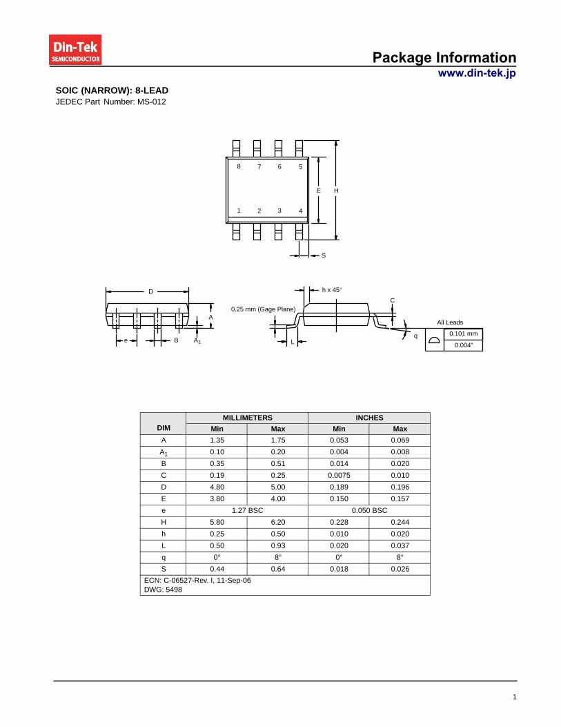
1
DIMMILLIMETERS INCHES
Min Max Min Max
A 1.35 1.75 0.053 0.069
A1 0.10 0.20 0.004 0.008
B 0.35 0.51 0.014 0.020
C 0.19 0.25 0.0075 0.010
D 4.80 5.00 0.189 0.196
E 3.80 4.00 0.150 0.157
e 1.27 BSC 0.050 BSC
H 5.80 6.20 0.228 0.244
h 0.25 0.50 0.010 0.020
L 0.50 0.93 0.020 0.037
q 0° 8° 0° 8°
S 0.44 0.64 0.018 0.026
ECN: C-06527-Rev. I, 11-Sep-06DWG: 5498
431 2
568 7
HE
h x 45
C
All Leads
q 0.101 mm
0.004"LB A1
A
e
D
0.25 mm (Gage Plane)
SOIC (NARROW): 8-LEADJEDEC Part Number: MS-012
S
Package Informationwww.din-tek.jp
1
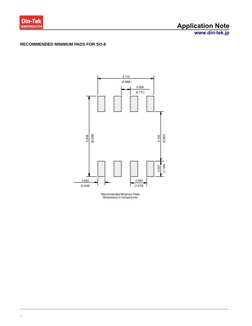
RECOMMENDED MINIMUM PADS FOR SO-8
0.24
6
(6.2
48)
Recommended Minimum PadsDimensions in Inches/(mm)
0.172
(4.369)
0.15
2
(3.8
61)
0.04
7
(1.1
94)
0.028
(0.711)
0.050
(1.270)
0.022
(0.559)
Application Notewww.din-tek.jp
1
DisclaimerALL PRODUCT, PRODUCT SPECIFICATIONS AND DATA ARE SUBJECT TO CHANGE WITHOUT NOTICE TO IMPROVERELIABILITY, FUNCTION OR DESIGN OR OTHERWISE.
Din-Tek Intertechnology, Inc., its affiliates, agents, and employees, and all persons acting on its or their behalf (collectively,“Din-Tek”), disclaim any and all liability for any errors, inaccuracies or incompleteness contained in any datasheet or in any otherdisclosure relating to any product.
Din-Tek makes no warranty, representation or guarantee regarding the suitability of the products for any particular purpose orthe continuing production of any product. To the maximum extent permitted by applicable law, Din-Tek disclaims (i) any and allliability arising out of the application or use of any product, (ii) any and all liability, including without limitation special,consequential or incidental damages, and (iii) any and all implied warranties, including warranties of fitness for particularpurpose, non-infringement and merchantability.
Statements regarding the suitability of products for certain types of applications are based on Din-Tek’s knowledge of typicalrequirements that are often placed on Din-Tek products in generic applications. Such statements are not binding statementsabout the suitability of products for a particular application. It is the customer’s responsibility to validate that a particularproduct with the properties described in the product specification is suitable for use in a particular application. Parametersprovided in datasheets and/or specifications may vary in different applications and performance may vary over time. Alloperating parameters, including typical parameters, must be validated for each customer application by the customer’stechnical experts. Product specifications do not expand or otherwise modify Din-Tek’s terms and conditions of purchase,including but not limited to the warranty expressed therein.
Except as expressly indicated in writing, Din-Tek products are not designed for use in medical, life-saving, or life-sustainingapplications or for any other application in which the failure of the Din-Tek product could result in personal injury or death.Customers using or selling Din-Tek products not expressly indicated for use in such applications do so at their own risk. Pleasecontact authorized Din-Tek personnel to obtain written terms and conditions regarding products designed for such applications.
No license, express or implied, by estoppel or otherwise, to any intellectual property rights is granted by this document or byany conduct of Din-Tek. Product names and markings noted herein may be trademarks of their respective owners.
Material Category PolicyDin-Tek Intertechnology, Inc. hereby certifies that all its products that are identified as RoHS-Compliant fulfill thedefinitions and restrictions defined under Directive 2011/65/EU of The European Parliament and of the Councilof June 8, 2011 on the restriction of the use of certain hazardous substances in electrical and electronic equipment(EEE) - recast, unless otherwise specified as non-compliant.
Please note that some Din-Tek documentation may still make reference to RoHS Directive 2002/95/EC. We confirm thatall the products identified as being compliant to Directive 2002/95/EC conform to Directive 2011/65/EU.
Din-Tek Intertechnology, Inc. hereby certifies that all its products that are identified as Halogen-Free follow Halogen-Freerequirements as per JEDEC JS709A standards. Please note that some Din-Tek documentation may still make referenceto the IEC 61249-2-21 definition. We confirm that all the products identified as being compliant to IEC 61249-2-21conform to JEDEC JS709A standards.
Legal Disclaimer Noticewww.din-tek.jp