Embed Size (px)
Citation preview

Muon Trigger Crate Manager (MTCM)Functional Description
FD-0129-01
Issue 4.00April 22, 2003
Prepared by:Ken Johns, Joel Steinberg
University of ArizonaTucson, Arizona


Ken Johns, Joel Steinberg April 22, 2003University of Arizona
Page 1
TABLE OF CONTENTS
1.0 INTRODUCTION................................................................................................................3
2.0 INPUTS/OUTPUTS............................................................................................................6
2.1 VME BUS (J1 CONNECTOR)................................................................................................62.2 CONNECTIONS TO MTCXX CARD (J2 AND J3 CONNECTORS) .......................................................6
2.2.1 J2 Connections ........................................................................................................62.3 SERIAL CONNECTIONS (J4, J7 AND J8 CONNECTORS) ...............................................................7
2.3.1 Serial Link to Muon Trigger Supervisory Crate (MTM_DATA).........................................82.3.2 Serial Link to Level 2 Trigger Framework (L2_DATA).................................................. 102.3.3 Serial Link to Level 3 Trigger Framework (L3_DATA).................................................. 102.3.4 Timing Signals ....................................................................................................... 102.3.5 MIL-STD-1553B Connection..................................................................................... 122.3.6 UART Interface....................................................................................................... 12
2.4 PARALLEL LINK FROM MRC (J6) ........................................................................................ 12
3.0 CONTROL/STATUS REGISTERS ..................................................................................... 14
3.1 MTCM EVENT STATUS REGISTERS..................................................................................... 143.2 MTCM ERROR WORD ..................................................................................................... 163.3 FPGA DOWNLOAD CONTROL REGISTER .............................................................................. 173.4 TIMING GENERATOR CONTROL REGISTER .............................................................................. 183.5 MESSAGE BUILDER CONTROL REGISTER............................................................................... 193.6 MTM MESSAGE CONTROL REGISTER .................................................................................. 203.7 TRIGGER LOGIC CONTROL REGISTER.................................................................................... 203.8 VME INTERFACE CONTROL REGISTER.................................................................................. 224.0 BUFFERING AND MESSAGE CONSTRUCTION ........................................................................... 234.1 MTCM BUFFERING.......................................................................................................... 234.2 MESSAGE CONSTRUCTION................................................................................................. 24
5.0 FRONT PANEL INDICATORS, SWITCHES AND TEST POINTS......................................... 27
5.1 FRONT PANEL INDICATORS (IN ORDER FROM TOP TO BOTTOM).................................................... 275.2 FRONT PANEL SWITCHES.................................................................................................. 275.3 FRONT PANEL TEST POINTS .............................................................................................. 28
APPENDIX A - BLOCK DIAGRAM OF MTCM ........................................................................A-1
APPENDIX B - J1 CONNECTIONS........................................................................................B-1
APPENDIX C - J2 CONNECTIONS.......................................................................................C-1
APPENDIX D - J3 CONNECTIONS........................................................................................D-1
APPENDIX E - J6 CONNECTIONS ........................................................................................E-1
APPENDIX F - MIL-STD-1553B.............................................................................................F-1
1.0 INTRODUCTION TO 1553B.................................................................................................F-12.0 1553B COMMANDS ........................................................................................................F-1
2.1 Sub Address Commands ..........................................................................................F-22.2 Mode Commands .....................................................................................................F-2
APPENDIX G - UART COMMUNICATIONS........................................................................... G-3

Ken Johns, Joel Steinberg April 22, 2003University of Arizona
Page 2
APPENDIX H - VME MEMORY MAPS ...................................................................................H-1
APPENDIX I - GLOSSARY.................................................................................................... I-1

Ken Johns, Joel Steinberg April 22, 2003University of Arizona
Page 3
1.0 Introduction
The Muon Trigger Crate Manager (MTCM) is one of a set of VME cards used to form the Level 1 (L1)muon trigger decision for Run 2 of D0. We presently envision a total of 3 such MT crates, one eachfor the CF, EFN and EFS geographic regions. The Muon Trigger Crate Manager resides in the 4thslot of each of the three MT crates which are located on the D0 detector platform. The physicallayout shown in Figure 1 shows the standard MT crate configuration with eight MTC05 and eightMTC10 cards and a 68xxx processor board. The eight MTC05 and MTC10 cards correspond tooctants within a given geographic region. MTCxx is used as shorthand when referring to MTC05 andMTC10 cards.
Figure 1 - Muon Trigger Crate
The configuration of the Muon Trigger Crate shown above is a “typical” configuration, showing 8 pairsof MTC05s and MTC10s. It is possible for the crate to be used in many different configurations bychanging the masks located in the MTCM VME memory.
There are 2 types of input signals received by the MTCM from the outside world, timing and control.The timing signals such as the 53 MHz RF Clock, First_Crossing and Sync Gap signals areconnected to the MTCM through coax cable from the Muon Readout Card (MRC). The controlsignals, which include trigger accepts and rejects, are connected to the MRC via a 50 pin twist andflat ribbon cable from the MRC.
The MTCM is constructed as a 9U x 400mm VME card and provides the following functions:
⇒ Receives and decodes timing information from the MRC. signals are the RF Clock,First_Crossing, Sync Gap and Gap signals. The Sync Gap and Gap signals are decodedfrom one signal line from the MRC. The timing signals received by the MTCM are bufferedand distributed to the MTCxx cards. The First_Crossing and Sync Gap signals arrive at theMTCM an arbitrary amount of time before the actual event in the accelerator turn. TheMTCM adjusts its BC counter in such a way that the First_Crossing signal is assigned the

Ken Johns, Joel Steinberg April 22, 2003University of Arizona
Page 4
appropriate crossing number. That is, the First_Crossing signal is assigned a preset BCnumber such that the BC number of the crossing in which the MTCM first sees data afterthe Sync Gap is 7. This is described further in the timing section of this document. Thusthe timing adjustment on the MTCM is to within 132 ns. A finer timing adjustment takesplace on the MTM card, which sends the global muon trigger decision to the TriggerFramework (TF).
⇒ Reads a total of 36 bits of card trigger decision information from each pair of MTC05 andMTC10 cards in the crate and forms a regional trigger decision often referred to as cratetrigger decision) based on these decisions. Sixteen bits of regional trigger information aresent to the Muon Trigger Manager (MTM) which combines this information with informationfrom the other two crates to form a global level 1 muon trigger decision. For each bunchcrossing the 192 bits of card trigger decision data (36 bits from each pair of MTC05 andMTC10 Cards), the 16 bits of regional trigger decision, the card status register and the carderror register are stored in a Dual Port Memory (DPM). The base address for the data isstored in the L1 pending FIFO, awaiting a decision from the Trigger Framework.
⇒ Receives trigger information such as L1 Accept, L2 Accept and Reject, Bunch CrossingNumber, etc. on a 50 conductor twist and flat cable from the MRC and passes this data tothe MTCxx cards in the crate.
⇒ Upon receipt of an L1 ACCEPT signal the MTCM reads the Card trigger decision data, thecard status register and the card error register from the DPM by getting the base addressfrom the FIFO. The MTCM also reads 16 bits of supplemental trigger decision data fromeach MTCxx over the VME bus. The MTCM then transmits all this data, along with aninternally generated BC number and turn number to the L2 muon trigger. The 16supplemental bits from each MTCxx are added to the DPM along with the other dataassociated with this BC. The base address of the data for the accepted BC is transferredfrom the L1 pending FIFO top the L2 pending FIFO.
⇒ Upon receipt of an L2 ACCEPT the MTCM reads from each MTCxx card its input data,card error and card status. The MTCM then sends the above data, along with its own cratedecision data, status and error data, and the cards trigger decisions and supplementaltrigger decision that are saved on the MTCM to the MRC for transfer to L3 via the VBD. Thedata from the MTCxxs is collected by the MTCM over the VME data bus lines by becomingbus master and reading the pointer from each MTCxx to determine where to get the datafrom.
⇒ The MTCM collects detected errors from itself and the MTCxx cards and sends an OR ofthese asynchronously to the MRC. Possible MTCM error conditions are discussed insection 2.3.1.2.
⇒ The MTCM collects Busy information for itself and each of the MTCxx cards. A logical ORof these busy signals is sent as L1 BUSY to the trigger framework via the MRC.
⇒ Upon receiving an initialization signal, the MTCM presets both the turn and BC number andclears all FIFOs and DPM pointer buffers on the MTCxx cards and itself.
⇒ Provides a LEMO output jack that supplies a NIM compatible signal to indicate a MTCMtrigger decision.
⇒ The MTCM contains an interface to the 1553 system. Any VME Location in the MTCMcrate can be written to or read from via the 1553 controls system.

Ken Johns, Joel Steinberg April 22, 2003University of Arizona
Page 5
⇒ The MTCM contains a serial UART connection to the MRC. Any VME Location in theMTCM crate can be written to or read from via the serial UART.
⇒ The logic for generating the crate trigger decisions is implemented in Field ProgrammableGate Arrays (FPGA) that can be changed from either the MIL-STD-1553B interface, theUART interface or directly over the VME bus. Most other logic, such as the logic thatcontrols the interfaces and timing, are programmed in FPGAs that can be reprogrammedusing a separate JTAG (Joint Test Action Group) connector that is compatible with IEEEStd 1149.1-1990.

Ken Johns, Joel Steinberg April 22, 2003University of Arizona
Page 6
2.0 Inputs/Outputs
2.1 VME Bus (J1 Connector)
The MTCM has a VME interface using 32 bit addressing and is capable of 32 bit data transfers. TheMTCM is capable of becoming bus master and transferring data from the MTCxx boards in the crateover the VME data bus. The MTCM VME Bus uses a 128 pin DIN Connector in order to combinethe functions usually found on J1 and J2 into one connector so that while it may work with any VMEsystem board it must be installed in the Muon Trigger Crate to operate. The pin assignments for J1can be found in Appendix B.
2.2 Connections to MTCxx Card (J2 and J3 Connectors)
The J2 and J3 connectors, which are both 96 pin DIN connectors, are used to communicatebetween the MTCM and the MTC05 and MTC10 cards that exist in the crate. Section 2.2.1describes these signals while the pin assignments for these signals may be found in Appendix C.
2.2.1 J2 Connections
The following is a list of the signals that exist on the J2 and J3 connectors. For each signal, wehave indicated the signal name, the type of signal (TTL, PECL, etc.), and the source and destinationof the signal. Actual pin assignments for J2 can be found in Appendix C.
⇒ M_CLOCK - (Differential PECL) - (from MTCM to MTCxxs) 8 differential signals that aredistributed one for each pair of MTC05 and MTC10 in the crate, this is the 53 MHz RF clockthat is received from the MRC.
⇒ CARD_TRIGGER_DATA[95..0] - (TTL) - (from each MTCxx to the MTCM) - 12 lines fromeach of the MTC05 and MTC10 card pairs (these lines are common from each card in thepair). The data is MTC10 data when L10-Enable is active and MTC05 data when L05-Enableis active.
⇒ BC_Trig[0:7] - (TTL, terminated on backplane) - (from MTCM to MTCxxs) - This buscontains the BC Number to associate with the data when the L1-ACCEPT signal is active.Note that the BC Number is only 8 bits, the other 7 bits are not defined as of this revision.
⇒ STORE_ALL - (TTL - terminated on backplane) - (from MTCM to MTCxxs) - This signal,which can only be active when L1 ACCEPT is active, indicates to the MTCxxs that the datafor the accepted BC needs to have all of its input data stored and made accessible to theVME bus for possible transmission to Level 3.
⇒ SEND_DATA (TTL – terminated on backplane) – (From MTCM to MTCxxs) – InstructsMTCxx boards to start transmiting data back to MTCM.
⇒ L05-ENABLE - (TTL, terminated on backplane) - (from MTCM to MTCxxs) - Enables theCard-Trigger-Data from the MTC05 card in a MTC05 and MTC10 pair
⇒ L10- ENABLE - (TTL, terminated on backplane) - (from MTCM to MTCxxs) - Enables theCard-Trigger-Data from the MTC10 card in a MTC05 and MTC10 pair
⇒ L1 ACCEPT - (TTL, terminated on the backplane) - (from MTCM to MTCxxs) - Signal toindicate that the crate has received a L1 ACCEPT for the last trigger candidate sent to theTrigger Framework and all data should be saved. This signal comes a set number ofcrossings after the data is sent to the trigger framework, any candidate that does notreceive an L1_ACCEPT is assumed to be rejected.

Ken Johns, Joel Steinberg April 22, 2003University of Arizona
Page 7
⇒ SYNCH GAP - (TTL, terminated on the backplane) - (from MTCM to MTCxxs) - This signalindicates that the beam is in the Synch Gap.
⇒ GAP - (TTL, terminated on the backplane) - (from MTCM to MTCxxs) - This signal indicatesthat the beam in a Gap of any type.
⇒ INPUT_READY - (Open Collector TTL, pulled up on the MTCM) - (from MTCxxs to MTCM) -This signal is a “wire-or” that contains a high level signal when all of the MTCxxs in thecrate have not empty conditions for all of the input FIFOs that have not been masked off.This signal is tested by the MTCM to confirm that it’s rising edge is at the expected time.
⇒ L2 ACCEPT - (TTL, terminated on the backplane) - (from MTCM to MTCxxs) - Signal toindicate that the Level 2 Trigger Framework has accepted a trigger candidate and that theaddress of the data should be made available in the Buffer Pointer FIFO.
⇒ L2 REJECT - (TTL, terminated on the backplane) - (from MTCM to MTCxxs) - Signal toindicate that the Level 2 Trigger Framework has rejected the trigger candidate and that thebuffer should be freed for use.
⇒ DATA_READY - (Open Collector TTL, pulled up on the MTCM) - (from MTCxxs to MTCM) -This signal is a “wire-or” that contains a high level signal when all of the MTCxxs in thecrate have data ready to transfer to the MTCM. Each MTCxx will release this signal whenall of it’s active serial inputs, that have not been masked off on initialization, have receivedat least one byte of data and the card has created it’s Card Trigger Data. This signal istested by the MTCM to confirm that it’s rising edge is at the expected time.
⇒ BC_CLOCK - (TTL, terminated on the backplane) - (From MTCM to MTCxxs) BC Clockcreated by the MTCM. This clock is a crate Bunch Crossing Clock that is synchronous withL05-ENABLE and L10-ENABLE.
⇒ LEVEL_1_BUSY* - (Open Collector TTL, pulled up on the MTCM) - “Wire-or” signal, eachMTCxx can cause this line to go low if there is a memory or FIFO full condition that wouldmake it impossible for the board to process a L1 ACCEPT signal.
⇒ LEVEL_2_BUSY* - (Open Collector TTL, pulled up on the MTCM) - “Wire-or” signal, eachMTCxx can cause this line to go low if there is a condition that make it impossible for theboard to process an L2 ACCEPT signal. This condition can occur if the DPM on the MTCxxbecomes nearly full, which is not expected given the anticipated acceptance rates.
⇒ LEVEL_1_ERROR* - (Open Collector TTL, pulled up on the MTCM) - “Wire-or” signal, eachMTCxx can cause this line to go low if there is an error condition that needs to be reportedto the MRC. A mis-match between the expected and received BC Number could cause thiserror for a L1 ACCEPT, L2 ACCEPT or L2 REJECT. An inoperative serial receiver on aMTCxx Card could also cause this error.
⇒ RESET_COUNTERS - (TTL, terminated on the backplane) - (from MTCM to MTCxxs) -Signal that causes the MTCxxs to reset their internal Bunch Crossing counters, indicatingthe beginning of a turn.
⇒ MASTER_RESET - (TTL, terminated on backplane) - (from MTCM to MTCxxs) - Masterreset generated from the initialize command that causes all internal counters, FIFOs andmemories to be reset to initial condition.
2.3 Serial Connections (J4, J7 and J8 Connectors)

Ken Johns, Joel Steinberg April 22, 2003University of Arizona
Page 8
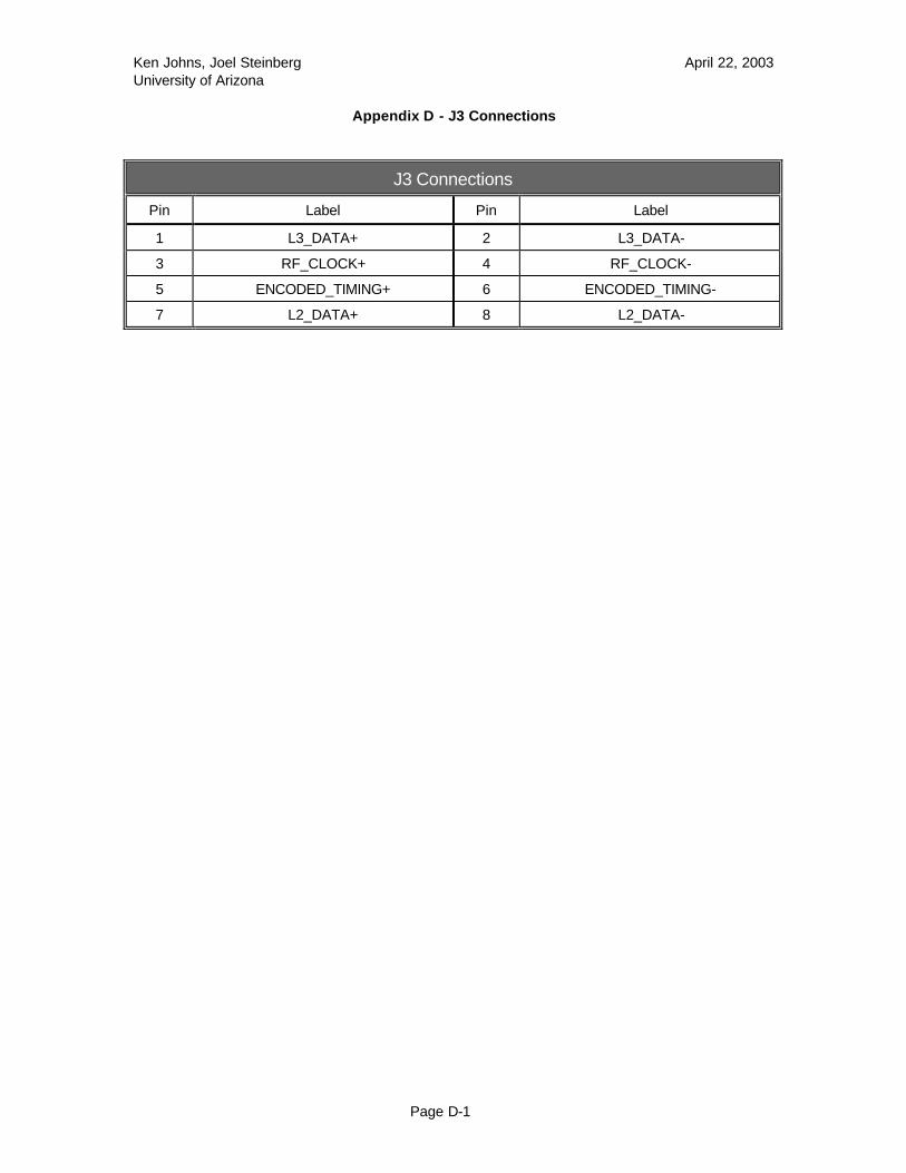
The serial connections on this board are through 2 coax connections on J4, a coax connector onthe front panel that connects to the MTT, 2 triax connectors (J7 and J8) for the MIL-STD-1553Binterface and 4 pins on the parallel link that connects the MRC to the MTCM (J6). J4 is an 8 pinAMP connector (p/n 103167-1), and the coax connector on the front panel that connects to the MTTis a BNC type connector. If any signals require fiber optic connections, a separate board will beused to convert the optical signal to an acceptable electrical signal. Pin Assignments for J3 areshown in Appendix D. All of these connectors are mounted on the front of the board.
2.3.1 Serial Link to Muon Trigger Supervisory Crate (MTM_DATA)
The regional or crate trigger decision from each MTCM is sent to the Muon Trigger Manager (MTM)card which sits in the Muon Trigger Supervisory crate. These crate trigger decisions are used by theMTM to form a global trigger decision, which is sent on to the Level 1 Trigger Framework. Triggerdecisions are only sent for BCs that can have a trigger (crossings that are not in the Sync Gap).Fiber Channel idle characters (K28.5) are sent for all those BCs that cannot have a trigger crossingthat are in the Sync gap). The trigger decision for each crate is sent via the AMCC S2042/S2043chipset to the MTM. The data sent on the serial link is as follows:
Word # Description
1 Start of Transmission
2 Crate Trigger Decision Word 1
3 Crate Trigger Decision Word 2
4 MTCM Error Word 1
5 MTCM Error Word 2
6 Unassigned
7 Parity
This serial link, located at J4 on the front of the MTCM, operates over RG58 (or equivalent) cable ata word rate of 53 MHz resulting in a serial bit rate of 1062 Mbps. The front panel connector isattached to a serial daughter board that is mounted on the MTCM, so that there is no actualconnection on the MTCM board itself for this signal.
The Crate Trigger Decision Words are described below, The MTCM Error Words are described insection 3.2.

Ken Johns, Joel Steinberg April 22, 2003University of Arizona
Page 9
2.3.1.1 Crate Trigger Decision Words
Byte.Bit Description
1.0 bit 0 of 2 bit counter for threshold pt1 sign0
1.1 bit 1 of 2 bit counter for threshold pt1 sign0
1.2 bit 0 of 2 bit counter for threshold pt1 sign1
1.3 bit 1 of 2 bit counter for threshold pt1 sign1
1.4 bit 0 of 2 bit counter for threshold pt2
1.5 bit 1 of 2 bit counter for threshold pt2
1.6 bit 0 of 2 bit counter for threshold pt3
1.7 bit 1 of 2 bit counter for threshold pt3
2.0 bit 0 of 2 bit counter for threshold pt4 (loose)
2.1 bit 1 of 2 bit counter for threshold pt4 (loose)
2.2 bit 0 of 2 bit counter for threshold pt4 (tight)
2.3 bit 1 of 2 bit counter threshold pt4 (tight)
2.4 bit 0 of 2 bit counter for no CFT trigger
2.5 bit 1 of 2 bit counter for no CFT trigger
2.6 Unassigned
2.7 Unassigned

Ken Johns, Joel Steinberg April 22, 2003University of Arizona
Page 10
2.3.2 Serial Link to Level 2 Trigger Framework (L2_DATA)
Upon receipt of a Level 1 Accept, the following information is sent to the Level 2 muon preprocessorfor use in the Level 2 muon trigger decision:
• Crate level trigger decision (16 bits)
• MTC05 and MTC10 card level trigger decisions (12 bits each)
• Supplemental trigger information from each card such as the eta or phi bins of foundtriggers (16 bits each card), status and error bits.
The format of the data is described in the D0note 3537, “Muon Data Formats to L2 & L3”. Themethod used to create the message in the MTCM is described in section 4.2.
This serial link, which is located in J3, operates at a byte rate of 16 MHz, resulting in a serial clockrate of 160 MHz. It will take up to 15µs to transfer the data to Level 2, which is longer than theexpected rate given the speed on the interface because of possible delays caused by the VMEinterface. This is still much shorter than the required time of 100µs for the L1 acceptance rate of 10kHz. This link is implemented using a Cypress HOTLink™ p/n CY7B923.
2.3.3 Serial Link to Level 3 Trigger Framework (L3_DATA)
This serial link, located on J3, transfers the data that the MTCM has collected from each MTCxxcard when a L2 Accept is received. The MTCM collects the data from each MTCxx using the VMEData Bus. The MTCM then formats the data and transmits it over the serial link. The format of thedata is described in the D0note 3537, “Muon Data Formats to L2 & L3”. The method used to createthe message in the MTCM is described in section 4.2.
The data is obtained by the MTCM from each MTCxx by first reading a pointer on each board andthen reading the data from the address that is pointed to. Since all of the MTCxx boards have thesame L1 and L2 Accepts, this pointer should be the same for all boards, and an error is flagged if itis not. Some of the data that can be collected from the MTCxx cards is only transmitted for 1 of nL1 accepts, as specified in the control word for the MTCM.
The serial link will operate at a byte rate of 16 MHz, resulting in a serial clock rate of 160 MHz. Itwill take up to 500µs to transfer the data for a complete message to Level 3, which is longer thanthe expected rate given the speed on the interface because of possible delays caused by the VMEinterface. This is less than the required time of 1,000µs for the L2 acceptance rate of 1 kHz. Thislink is implemented using a Cypress HOTLink™ p/n CY7B923.
2.3.4 Timing Signals
There are 2 signals that are used to synchronize the MTCM to the rest of the system. Thesesignals originate at the Trigger Framework, are transported over the Serial Command Link to theMuon Fanout Card, distributed over the VME backplane to the Muon Readout Cards and sent viacoaxial ASTRO cable to the MTCM on connector J3 along with L2_DATA and L3_DATA. Thesesignals must be adjusted digitally so that their relationship to the incoming data is correct. Thereare 2 other signals generated by the MTCxxs that are used to check that timing is correct, thesesignals are Data_Ready and Input_Ready.
⇒ RF_Clock - 53 MHz Clock that is the basic accelerator RF signal. This signal is not used inthe MTCM at this time.
Ken Johns, Joel Steinberg April 22, 2003University of Arizona
Page 11
⇒ Encoded_Timing - This is a Manchester encoded signal that runs at twice the RF_Clockrate. This signal is used to generate internal MTCM signals that indicate the First Crossingtime, Gap and Sync Gap times. The clock from the decoder circuit is divided by 2 and usedas the local RF Clock, instead of the RF_Clock signal since it is phase aligned with thedecoded timing signals. The decoded timing signals are described below.
• First Crossing indicates the beginning of a turn. The First Crossing signal is associatedwith the sixth bunch crossing before the first bunch crossing that contains real beam,in other words, if First Crossing is called beam crossing 1 then beam crossing 7 will bethe first beam crossing that contains real data. The actual timing of the First Crossingsignal on the MTCM is adjusted so that the data for the first bunch crossing thatcontains real beam is at the MTCxxs on bunch crossing 7. The amount of adjustmentrequired will be determined during installation of the MTCM and will thereafter bechecked by the MTCM and Input Ready and Data Ready Errors generated if the data isnot arriving at the proper time. The MTCM also checks that the First Crossing pulse isoccurring at the proper time with respect to it’s internal counter and will report anydiscrepancy with a First Crossing Timing Error. First Crossing also causes the bunchcrossing counter to be preset and the internal Turn Number on the MTCM to be resetfor the first First Crossing signal received after an INITIALIZE signal.
• The Gap signal indicates any superbunch gap. The Logic for the MTCM triggergeneration will be different during these gaps than when beam is present.
• The Sync Gap indicates the superbunch gap during which no crossing is allowed togenerate a L1 accept, as well as other gaps. The Sync Gap is used to allow the inputFIFOs to empty (and thus become synchronized later when they are all not empty).The Sync Gap also allows the logic to “catch up” after Level 1 accepts in the previousturn. Note that only one of the three superbunch gaps is a Sync Gap. Cosmic ray,pulser and other triggers are permitted during the other 2 gaps. During the Synch Gap,all front ends will send idle signals (K28.5 as defined in the Fiber Channel specification)over their serial outputs to the MTCxxs. The idle characters maintain wordsynchronization at the MTCxx.
Another signal related to timing is INIT, which is sent over the 50-conductor cable from the MRC. Onreceipt of INIT the MTCM will complete any transfers to L2 or the MRC which are in progress beforeinitializing the crate, which includes for the MTCM:
⇒ Reset the Buffer Pending, L2 Pending and Buffer Transfer FIFOs
⇒ Initialize the Empty Buffer FIFO by writing in a list of all DPM addresses
⇒ Transmit the MASTER_RESET signal to the MTCxx boards so that they will all beinitialized
The MTCM will raise the BUSY1 flag in response to the INIT signal (or leave it raised if it wasalready up when the INIT is received). BUSY1 will stay active until the MTCM is ready to take data.BUSY1 will always be active a minimum of 1.5 µs. The MTCM will transmit SYNC characters overthe serial links to the MTM, L2 and the MRC when it is not sending actual data in order to maintainsyncronization on these links.
The first FIRST_CROSSING signal received after a power cycle or INITIALIZE signal is used to setthe internal BC counter to the proper number and reset the turns counter. SubsequentFIRST_CROSSING signals are used to check that the BC counter is at the proper count whenFIRST_CROSSING is received, and to report an error if it is not.

Ken Johns, Joel Steinberg April 22, 2003University of Arizona
Page 12
The MTCM monitors the INPUT_READY and DATA_READY backplane signals to determine thatthey occur at the proper times. The measured times (in BC clock ticks) from receivingFIRST_CROSSING receiving INPUT_READY and DATA_READY is available in VME memory to themonitoring system and can be used for debugging purposes. INPUT_READY indicates when allunmasked inputs on all MTCxx boards are not empty, and DATA_READY indicates when allMTCxx boards have trigger decisions ready for transfer to the MTCM. These signals are obviouslyclosely related and are included to simplify error detection and debugging.
2.3.5 MIL-STD-1553B Connection
There is access to the memory of the crate via a MIL-STD-1553B port that is located on the frontpanel of the module. Details on using this port are contained in Appendix F.
2.3.6 UART Interface
There is access to the memory of the crate via a high speed UART connection to the MRC. Detailson using this port are contained in Appendix G, these signals are connected using 4 pins on theparallel link from the MRC (J6).
2.4 Parallel Link from MRC (J6)
There is a 50-conductor twist and flat cable that is used to communicate between the MTCM andthe MRC using differential ECL signals. J6 is located on the front of the MTCM board. The pinoutsfor this connector are shown in Appendix E. Following is a list of the signals that are found on thiscable.
⇒ XING0 - XING7 - (from MRC to MTCM) - 8 bit number in the range of 1 to 159 that indicatesthe BC when the L1 Accept signal is active
⇒ INITIALIZE - (from MRC to MTCM) - This signal causes all internal registers, memories andFIFOs to be cleared, except for error registers, which are maintained until read. The errorregisters will be read out through the internal UART after being polled by the controlsystem. INITIALIZE may also cause other reset sequences, such as using the Built In SelfTest feature of the outgoing serial links to L2 and L3, and will maintain a BUSY state untilall such sequences are completed, BUSY will always be active a minimum of 1.5 µs.
⇒ L1_ACCEPT - (from MRC to MTCM) - Signal indicates that the BC number contained inXING0 to XING7 was accepted. All data associated with this crossing will be maintained(both in the MTCM and the MTCxxs) and the L2_DATA message described in 2.3.2 will betransmitted.
⇒ L2_ACCEPT - (from MRC to MTCM) - Signal indicates that the next BC number awaiting aL2 decision (i.e. a BC that has previously had a L1_ACCEPT) has been accepted. TheMTCM determines if this is a 1 of n acceptance and sends the full L2_TRIG described in2.3.3 if it is or a truncated message if it is not. After collecting the data for this transfer fromeach MTCxx, the MTCM frees the buffer area in each MTCM that had been used for thisevent, as well as it’s own buffer area.
⇒ L2_REJECT - (from MRC to MTCM) - Signal indicates that the next BC number awaiting aL2 decision (i.e. a BC that has previously had a L1_ACCEPT) has been rejected. TheMTCM informs the MTCxxs, which causes them to clear their buffers, and clears it’s ownbuffer for this BC.

Ken Johns, Joel Steinberg April 22, 2003University of Arizona
Page 13
⇒ UART_XMIT - (from MRC to MTCM) - Serial communications line from MRC. Normally usedto request error transmission during initialization process, but can be used for other controlfunctions.
⇒ BUFFER_AVAILABLE - (from MRC to MTCM) - Used to indicate that the MRC has bufferspace available to accept the L2_TRIG data required after a L2_ACCEPT is received. If thisline is not high, the MTCM will hold the L2_TRIG Data until the line goes high and the datacan be sent to the MRC.
⇒ STROB - (from MRC to MTCM) - Strobe signal used to time all data from the MRC, data isvalid on rising edge of this signal.
⇒ UART_RCV - (from MTCM to MRC) - Serial communications line to the MRC. Normallyused transmit error codes when requested by MRC, but can also be used for other controlfunctions. This signal will never transmit, except when requested to with an appropriatecommand sent over the UART_XMIT line.
⇒ ERROR1 - (from MTCM to MRC) - This signal indicates that a Level 1 error has beendetected in the crate. Bad serial links, mis-matched BC counters, VME bus error, or otherdetectable errors may cause level 1 errors. This is a latched signal that will stay activeonce set until an INITIALIZE signal is received. The cause of this error is also latched andwill not be reset until the latched error register is overwritten. The individual contributors tothis mask may be disabled by setting the ERROR1 mask in VME memory, the errorregister will still contain the error condition but any bits that are masked will not cause anERROR1.
⇒ BUSY1 - (from MRC to MTCM) - This signal indicates that the MTCM has 16 L1 Acceptsthat have not been acknowledge with an L2 Accept or L2 Reject and that the crate canprocess no more L1_ACCEPTS until this signal goes low. BUSY1 will also be active inresponse to an INIT signal and stay low until the MTCM is ready to accept data. BUSY1will always be active for a minimum of 1.5 µs.
⇒ BUSY2 - (from MRC to MTCM) - This signal indicates that the MTCM can process no moreL2 accepts, at this writing there are no known cases that can cause this condition.

Ken Johns, Joel Steinberg April 22, 2003University of Arizona
Page 14
3.0 Control/Status Registers
There are several registers in defined in VME memory that allow the computer to monitor variousstatus conditions and control the operation of the logic in the MTCM.
3.1 MTCM Event Status Registers
These registers correspond to the Event Status Registers described in D0note 3537, “Muon DataFormats to L2 and L3”
Event Status Register 1
Byte.Bit Write Description Read Description
1.0 - MTCM VME Error
1.1 - MTCxx Error
1.2 - Timing Error
1.3 - MTCM L1 BC Error
1.4 - L2 Accept/Reject BC Error
1.5 - MRC Buffer_Available Error
1.6 -
1.7 -
2.0 -
2.1 -
2.2 Alignment Constant Set 0 Alignment Constant Set 0
2.3 Alignment Constant Set 1 Alignment Constant Set 1
2.4 Alignment Constant Set 2 Alignment Constant Set 2
2.5 Alignment Constant Set 3 Alignment Constant Set 3
2.6 Alignment Constant Set 4 Alignment Constant Set 4
2.7 Alignment Constant Set 5 Alignment Constant Set 5
The errors in Event Status Register 1, except for Timing Error, are all contained in the MTCM ErrorWord and are defined in section 3.2. The timing error is the logical OR of The five errors in theMTCM Error Word that are related to timing.
Since the Event Status Register is in normal memory, it is necessary to rewrite the AlignmentConstant set number after a power cycle.

Ken Johns, Joel Steinberg April 22, 2003University of Arizona
Page 15
Event Status Register 2
Byte.Bit Write Description Read Description
1.0 Calibration Constant Set 0 Calibration Constant Set 0
1.1 Calibration Constant Set 1 Calibration Constant Set 1
1.2 Calibration Constant Set 2 Calibration Constant Set 2
1.3 Calibration Constant Set 3 Calibration Constant Set 3
1.4 Calibration Constant Set 4 Calibration Constant Set 4
1.5 Calibration Constant Set 5 Calibration Constant Set 5
1.6 Calibration Constant Set 6 Calibration Constant Set 6
1.7 Calibration Constant Set 7 Calibration Constant Set 7
2.0 Calibration Constant Set 8 Calibration Constant Set 8
2.1 Calibration Constant Set 9 Calibration Constant Set 9
2.2 Calibration Constant Set 10 Calibration Constant Set 10
2.3 DSP Code Version # 0 DSP Code Version # 0
2.4 DSP Code Version # 1 DSP Code Version # 1
2.5 DSP Code Version # 2 DSP Code Version # 2
2.6 - -
2.7 - -
Event Status Register 2 is in Non-Volatile memory, so it is not necessary to rewrite this data after apower cycle.

Ken Johns, Joel Steinberg April 22, 2003University of Arizona
Page 16
3.2 MTCM Error Word
Byte.Bit Description
1.0 First_Crossing BC Error
1.1 Data_Ready BC Error
1.2 Input_ready BC Error
1.3 Sync Gap Start BC Error
1.4 Sync Gap End BC Error
1.5 MTCM L1 BC Error
1.6 L2 Accept/Reject BC Error
1.7 MTCM VME Error
2.0 MTCxx Error
2.1 MRC Buffer_Available Error
2.2 Supplememtal_Data_Pointer_Error
2.3 Transfer Data Pointer Error
2.4 Lock_Detect_Error
2.5 Buffer_Available_Error
2.6 Unassigned
2.7 Unassigned
The error are defined as follows:
⇒ First_Crossing BC Error, Data_Ready BC Error, Input_Ready BC Error, Sync Gap Start Errorand Sync Gap End Error are all timing related errors. During initialization, these 5 events areassigned an expected Bunch Crossing Number and the internal BC counter in the MTCM isadjusted so that the First Crossing signal received from the MRC is at the correct time.Subsequently, all the signals are checked to ensure that they have occurred at the correcttime, should any of them occur at the wrong time (or not at all) the appropriare error will besignaled. The logical OR of these 5 signals is used to create the Timing Error used in EventStatus Register 1 discussed in the previous section.
⇒ MTCM L1 BC Error – These errors are generated when the BC number sent from the MRC onL1 Accepts does not agree with the BC number of the event stored in the Dual Port Memory ofthe MTCM as described in section 4.1.
⇒ L2 Accept/Reject BC Error – This error is generated whenever the BC number sent from theMRC on L2 Accept or Reject does not agree with the BC number of the event stored in the DualPort Memory of the MTCM as described in secrion 4.1.
⇒ MTCM VME Error indicates that the MTCM has detected a VME bus error, such as a timeout.
⇒ MTCxx Error is generated if any of the MTCxxs in the crate detects anty error.

Ken Johns, Joel Steinberg April 22, 2003University of Arizona
Page 17
⇒ MRC Buffer Available Error – This error occurs if the MTCM needs to transmit a message to theLevel 3 Trigger Framework as a result of receiving a L2 Accept and the buffer on the MRC is notavailable. The MTCM waits for a time set by the Buffer Available Time Out register beforesending this error, the maximum time that can be set for this purpose is approximately 8.5msec.
⇒ Supplemental Data Pointer Error is generated if the MTCM detects that any of the MTCxx hasan incorrect pointer to the Supplemental Data used on an L1 Accept.
⇒ Transfer Data Pointer Error indicates that the MTCM has detected that at least one of theMTCxxs has an incorrect pointer to the data to be used on an L2 Accept.
⇒ Lock Detect Error indicates that at least one of the MTCxxs has at least one receiver that is notlocking to the incoming data (This is only detected for receivers that are not masked out)
⇒ Buffer Available error is generated if there are no local buffers available for storing L1 accepts,this error also causes a L1 Busy signal.
Note that there are two separate error registers maintained on the MTCM. The first is updated every132 ns. It is the memory location that is included in the MTCM data to L2 and the MRC foraccepted events. Bits in the second error register are latched whenever an error occurs and remainthere until specifically cleared (i.e. a 0 is written to that memory location).
Each bit in the Event Error Register can be masked out with a one in the correspoding bit in theError1 Mask Register. The mask prevents the corresponding bit in the latched register from beingset but the bit can still be read in the event register.
3.3 FPGA Download Control Register
This register controls the circuit that downloads the non-volatile memory into the Message Builderand Trigger Logic FPGAs.
Byte.Bit Write Description Read Description
1.0 - -
1.1 Load MTCM Logic FPGA MTCM Logic FPGA loaded
1.2 Load Message FPGA Message FPGA loaded
1.3 - MTCM Logic Load Error
1.4 - Message Load Error
1.5 - -
1.6 - -
1.7 Select MTCxx Test Data Confirm MTCxx Test Data
2.0 - -
2.1 - -
2.2 - -
2.3 - -

Ken Johns, Joel Steinberg April 22, 2003University of Arizona
Page 18
2.4 - -
2.5 - -
2.6 - -
2.7 Reset FPGA Download -
The Checksum data for each FPGA is stored in the memory along with the program data for thatFPGA, this checksum is transmitted with the data and is checked whenever the board is reset orthe FPGA data is reloaded into the device.
3.4 Timing Generator Control Register
Byte.Bit Write Description Read Description
1.0 - -
1.1 - -
1.2 - -
1.3 - -
1.4 - -
1.5 - -
1.6 - -
1.7 - -
2.0 - -
2.1 - -
2.2 - -
2.3 - -
2.4 - -
2.5 - -
2.6 - -
2.7 Programmed Initialize -

Ken Johns, Joel Steinberg April 22, 2003University of Arizona
Page 19
3.5 Message Builder Control Register
Byte.Bit Write Description Read Description
1.0 Transmit L2 Test Data L2 Test Data Done
1.1 Transmit L3 Test Data L3 Test Data Done
1.2 BIST type 1 for L2 Data Confirm BIST for L2 Data
1.3 BIST type 2 for L2 Data Confirm BIST for L2 Data
1.4 BIST type 1 for L3 Data Confirm BIST for L3 Data
1.5 BIST type 2 for L3 Data Confirm BIST for L3 Data
1.6 - -
1.7 Watchdog Error Reset Watchdog Error
2.0 - -
2.1 - -
2.2 - -
2.3 - -
2.4 - -
2.5 - -
2.6 - -
2.7 Reset Message Builder StateMachine
Message Builder StateMachine in Idle

Ken Johns, Joel Steinberg April 22, 2003University of Arizona
Page 20
3.6 MTM Message Control Register
Byte.Bit Write Description Read Description
1.0 BC0 to Transmit Test Data BC0 to Transmit Test Data
1.1 BC1 to Transmit Test Data BC1 to Transmit Test Data
1.2 BC2 to Transmit Test Data BC2 to Transmit Test Data
1.3 BC3 to Transmit Test Data BC3 to Transmit Test Data
1.4 BC4 to Transmit Test Data BC4 to Transmit Test Data
1.5 BC5 to Transmit Test Data BC5 to Transmit Test Data
1.6 BC6 to Transmit Test Data BC6 to Transmit Test Data
1.7 BC7 to Transmit Test Data BC7 to Transmit Test Data
2.0 Rotation Divider 0 Rotation Divider 0
2.1 Rotation Divider 1 Rotation Divider 1
2.2 Rotation Divider 2 Rotation Divider 2
2.3 Rotation Divider 3 Rotation Divider 3
2.4 Rotation Divider 4 Rotation Divider 4
2.5 Rotation Divider 5 Rotation Divider 5
2.6 Rotation Divider 6 Rotation Divider 6
2.7 Rotation Divider 7 Rotation Divider 7
When the MTCxx Test Data is selected instead of the backplane data from the MTCxxs, the testdata is sent to the MTM during 1 bunch crossing per rotation, the lower 8 bits of this register selectwhich bunch crossing the data will be sent on. The upper eight bits of this regsiter control how oftenthe data is sent, a zero sends the data every rotation, a one every other rotation, etc.

Ken Johns, Joel Steinberg April 22, 2003University of Arizona
Page 21
3.7 Trigger Logic Control Register
Byte.Bit Write Description Read Description
1.0
1.1
1.2
1.3
1.4
1.5
1.6
1.7
2.0
2.1
2.2
2.3
2.4
2.5
2.6
2.7

Ken Johns, Joel Steinberg April 22, 2003University of Arizona
Page 22
3.8 VME Interface Control Register
Byte.Bit Write Description Read Description
1.0 Initiate Interrupt A
1.1 Initiate Interrupt B
1.2
1.3
1.4
1.5
1.6
1.7
2.0
2.1
2.2
2.3
2.4
2.5
2.6
2.7 Software Reset
The “Soft” Reset provides a method to restore the message builder to an idle state if it gets into anunusable state for any reason. This reset can be actuated through software in the Status/Controlword or through the backplane VME reset.
Ken Johns, Joel Steinberg April 22, 2003University of Arizona
Page 23
4.0 Buffering and Message Construction
4.1 MTCM Buffering
The following data must be buffered on the MTCM card:
⇒ Card Errors associated with the event (16 bits occurring for each bunch crossing)
⇒ Card Status associated with the event (16 bits occurring for each bunch crossing)
⇒ Bunch Crossing Number as determined by the card (8 active bits occurring for eachbunch crossing, although all 16 bits are stored)
⇒ Turn Number as determined by the card (16 bits)
⇒ L1 Crate Decision Data (16 bits occurring for each bunch crossing)
⇒ MTC05 L1 Trigger Decision Data (96 bits (12 for each MTC05 Card) occurring for eachbunch crossing)
⇒ MTC10 L1 Trigger Decision Data (96 bits (12 for each MTC10 Card) occurring for eachbunch crossing)
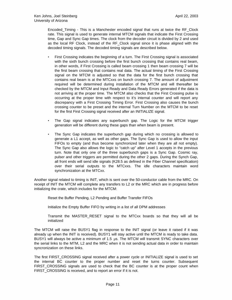
This data is stored in 3 write cycles for each bunch crossing that contains valid data (bunchcrossings not in the sync gap), one of the cycles is 3 RF Clock cycles long (56.4ns), while theother 2 writes are 2 RF Clock cycles (37.6ns). The first write is used to store the Card Errors,Bunch Crossing Number, The first group of Trigger Decision Data, and the L1 Crate Decision Data.The second write is used to store the Card Status, Turn Number, and the second group of TriggerDecision Data. The third write is used to store the third group of Trigger Decision Data. All of thisdata is stored directly into DPMs as it is received and pointers to the data are kept in FIFOs. TheDPM’s are then used to provide all three levels of required buffering for the MTCM. A block diagramof the buffering for the MTCM is shown in Figure 2. The block diagram shows a signal called L1Reject. This signal is produced on the MTCM and is active for any bunch crossing received from theMRC that could have an L1 Accept but does not, in other words any bunch crossing that does notcorrespond to data that would have been processed during the sync gap.
There are 9 16 bit wide DPMs, 6 for the MTCxx Trigger Decision/Supplemental Data and 1 each forthe L1 Crate Decision Data, Bunch/Turn Counters and Status/Error registers. The MTCxx Data isstored in 2 96 bit wide locations for each bunch crossing. Supplemental Trigger Decision Data (16bits for each MTCxx card) is buffered in a DPM on each MTCxx. For L1 Accepts, the SupplementalTrigger Decision Data is read from the MTCxx DPM by the MTCM.
Ken Johns, Joel Steinberg April 22, 2003University of Arizona
Page 24
Figure 2
4.2 Message Construction
The MTCM is responsible for constructing the message on the serial links to the Level 2 TriggerFramework and Level 3 Trigger Framework. The contents of the messages are described in 2.3.2and 2.3.3. Once the MTCM logic determines that a message needs to be transmitted over one ofthese links (because of receiving a L1 Accept or a L2 Accept signal from the MRC), the MTCM
starts reading a message script from the Script Memory. The Script Memory is a non-volatilememory that contains the script for 6 possible messages, a short message to L2, a long messageto L2, a test message to L2, a short message to L3, a long message to L3 and a test message to
Table 1
Script Address
L2 Long Message 1088 0000h – 1088 1FFCh
L2 Short Message 1088 2000h – 1088 2FFCh
L2 Test Message 1088 3000h – 1088 3FFCh
L3 Long Message 1088 4000h – 1088 5FFCh
L3 Short Message 1088 6000h – 1088 6FFCh
L3 Test Message 1088 7000h – 1088 7FFCh

Ken Johns, Joel Steinberg April 22, 2003University of Arizona
Page 25
L3. Table 1 lists the address range for the 6 scripts. The decision to send a long or short messageis set up in control registers in the Message Builder and can be fixed or a 1 of n type signal. ABlock Diagram of the message builder is shown in Figure 3, and a summary of the scriptcommands is shown in Table 2. The script commands allow the MTCM to read data, and transmitit, from each MTCxx or the MTCM based on the output of the pending FIFOs. There are alsocommands that allow the MTCM to to read data from anywhere within the MTCM, any MTCxx or themain processor board.
The non-volatile memory used for storing the message scripts is a “shadow” type memory, that isthe data is stored in normal RAM that is transferred to a “shadow” PROM whenever a write is doneto location 1088Fxxxh. The PROM data is automatically retrieved when the MTCM is powered on orwhen a read is made from location 1088Fxxxh.
Message BuilderFPGA
"Script"Dual Port Memory
("Left" Side)
CE
OE
LA[0:11]
LDATA[0:31]
VME_Address[00:31]
Read_Request
L2_ENN
L2_Data[0:7]
L2_ENA
L2_BIST
L3_ENN
L3_Data[0:7]
L3_ENA
L3_BIST
L2_Pend_Empty
L2_Pending_Data[0:8]
Transfer_FIFO_Empty
Transfer_FIFO_Data[0:8]
Bus_Granted
Data_Acknowledge
Data[0:31]
Figure 3 - Message Builder

Ken Johns, Joel Steinberg April 22, 2003University of Arizona
Page 26
Table 2 – Message Script
Script Data (SD) VME Address
SD[31..28] SD[27..24]
Action
A[31..28] A[27..24] A[23..1]
1 X Read 32 bits from VMEand XMIT 4 bytes
0 SD[27..24] SD[23..1]
2 X Read 16 bits from VMEand XMIT 2 bytes
0 SD[27..24] SD[23..1]
3 X Read 32 bits from VMEand XMIT 4 bytes
1
(MTCM)SD[27..24] A[23..16] = SD[23..16]
A[15..7] = FIFO A[6..1] =SD[6..1]
4 X Read 16 bits from VMEand XMIT 2 bytes
1
(MTCM)SD[27..24] A[23..16] = SD[23..16]
A[15..7] = FIFO A[6..1] =SD[6..1]
5 X Read 32 bits from VMEand XMIT 4 bytes
2
(MTCxx)SD[27..24] A[23..16] = SD[23..16]
A[15..7] = FIFO A[6..1] =SD[6..1]
6 X Read 16 bits from VMEand XMIT 2 bytes
2
(MTCxx)SD[27..24] A[23..16] = SD[23..16]
A[15..7] = FIFO A[6..1] =SD[6..1]
7 0 for data
1 for control
Transmit SD[15..0] as 2bytes of data or
SD[7..0] as a controlcharacter
- - -
8 X Read 32 bits from VMEand XMIT 4 bytes
1
(MTCM)SD[27..24] SD[23..1]
9 X Read 16 bits from VMEand XMIT 2 bytes
1
(MTCM)SD[27..24] SD[23..1]
A X Read 32 bits from VMEand XMIT 4 bytes
2
(MTCxx)SD[27..24] SD[23..1]
B X Read 16 bits from VMEand XMIT 2 bytes
2
(MTCxx)SD[27..24] SD[23..1]
C X Read Pending Pointer 2
(MTCxx)SD[27..24] H”000016”
D X Read Transfer Pointer 2
(MTCxx)SD[27..24] H”000026”
E X Move Transfer Pointerto Empty Buffer List
2
(MTCxx)SD[27..24] H”000026”
0,F X End Message - - -

Ken Johns, Joel Steinberg April 22, 2003University of Arizona
Page 27
5.0 Front Panel Indicators, Switches and Test Points
5.1 Front Panel Indicators (in order from top to bottom)
⇒ VME Data Acknowledge (Green) (D14b)
⇒ TRIG (Green) (D14a)
(Indicates an active output from board, logical OR of MTCM output bits)
⇒ L1 Accept (Green) (D7b)
⇒ L1 Reject (Green) (D7a)
⇒ L2 Accept (Green) (D6b)
⇒ L2 Reject (Green) (D6a)
⇒ First_Crossing Bunch Crossing Error (Red) (D5b)
⇒ Sync Gap Start or End Error (Red) (D5a)
⇒ Data Ready Bunch Crossing Error (Red) (D4b)
⇒ Input Ready Bunch Crossing Error (Red) (D4a)
⇒ Pointer Error (Red) (D11b)
⇒ MRC Buffer Available Error (Red) (D11a)
⇒ MTCxx Error (Red) (D13b)
⇒ VME Error (Red) (D13a)
⇒ 1553B Interface Active (Green) (D12a)
⇒ UART Interface Active (Green) (D12b)
⇒ +5v Power Supply Good (Yellow) (D8)
⇒ +3.3v Power Supply Good (Yellow) (D9)
⇒ -12v Power Supply Good (Yellow) (D10)
5.2 Front Panel Switches
There are no Front Panel Switches

Ken Johns, Joel Steinberg April 22, 2003University of Arizona
Page 28
5.3 Front Panel Test Points
NIM compatible versions of the following signals are available for monitoring on the front panel (inorder from top to bottom):
⇒ FIRST_CROSSING (J9a)
⇒ SYNC_GAP (J9b)
⇒ DATA_READY (J10b)
⇒ INPUT_READY (J10a)
⇒ MTCM Crate Decision (Fast OR) (J11a)
⇒ BC Clock (J11b)
Ken Johns, Joel Steinberg April 22, 2003University of Arizona
Page A-1
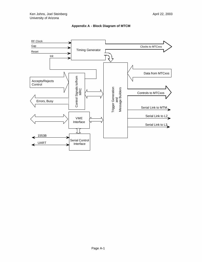
Appendix A - Block Diagram of MTCM
RF Clock
Timing GeneratorGap
Reset
Init
Trig
ger G
ener
atio
n
an
d M
essa
ge B
uild
ers
VMEInterface
Clocks to MTCxxs
Con
trol S
igna
ls to
/from
MR
C
Data from MTCxxs
Controls to MTCxxs
Serial Link to MTM
Serial Link to L2
Serial Link to L3
Accepts/RejectsControl
Errors, Busy
Serial ControlInterface
1553B
UART

Ken Johns, Joel Steinberg April 22, 2003University of Arizona
Page B-1
Appendix B - J1 Connections
J1 Connections
Pin Label Pin Label Pin Label
A1 DATA00 B1 BBSY* C1 DATA08
A2 DATA01 B2 BCLR* C2 DATA09
A3 DATA02 B3 C3 DATA10
A4 DATA03 B4 C4 DATA11
A5 DATA04 B5 +5V C5 DATA12
A6 DATA05 B6 C6 DATA13
A7 DATA06 B7 +5V C7 DATA14
A8 DATA07 B8 C8 DATA15
A9 GND B9 +5V C9 GND
A10 B10 BG3-IN* C0 SYSFAIL*
A11 GND B11 +5V C1 BERR*
A12 DS1* B12 C2 SYSRESET*
A13 DS0* B13 C3 LWORD*
A14 WRITE* B14 C4 AM5
A15 GND B15 BR3* C5 ADDR23
A16 DTACK* B16 AM0 C16 ADDR22
A17 GND B17 AM1 C17 ADDR21
A18 AS* B18 AM2 C18 ADDR20
A19 GND B19 AM3 C19 ADDR19
A20 B20 GND C20 ADDR18
A21 IACKIN* B21 +5V C21 ADDR17
A22 B22 +5V C22 ADDR16
A23 AM4 B23 GND C23 ADDR15
A24 ADDR07 B24 C24 ADDR14
A25 ADDR06 B25 C25 ADDR13
A26 ADDR05 B26 C26 ADDR12
A27 ADDR04 B27 C27 ADDR11
A28 ADDR03 B28 C28 ADDR10
A29 ADDR02 B29 IRQ2* C29 ADDR09
A30 ADDR01 B30 IRQ1* C30 ADDR08
A31 -12V B31 +5V C31
A32 +5V B32 +5V C32 +5V

Ken Johns, Joel Steinberg April 22, 2003University of Arizona
Page B-2
J1 Connections
Pin Label Pin Label
D1 +5V Z1
D2 GND Z2 GND
D3 +5V Z3
D4 +5V Z4 GND
D5 +5V Z5
D6 Z6 GND
D7 Z7
D8 +5V Z8 GND
D9 T_D84 Z9 T_D72
D10 Z10 GND
D11 T_D85 Z11 T_D73
D12 +3.3V Z12 GND
D13 T_D86 Z13 T_D74
D14 +3.3V Z14 GND
D15 T_D87 Z15 T_D75
D16 +3.3V Z16 GND
D17 T_D88 Z17 T_D76
D18 +3.3V Z18 GND
D19 T_D89 Z19 T_D77
D20 +3.3V Z20 GND
D21 T_D90 Z21 T_D78
D22 +3.3V Z22 GND
D23 T_D91 Z23 T_D79
D24 +3.3V Z24 GND
D25 T_D92 Z25 T_D80
D26 +3.3V Z26 GND
D27 T_D93 Z27 T_D81
D28 +3.3V Z28 GND
D29 T_D94 Z29 T_D82
D30 +3.3V Z30 GND
D31 T_D95 Z31 T_D83
D32 +5V Z32 GND

Ken Johns, Joel Steinberg April 22, 2003University of Arizona
Page C-1
Appendix C - J2 Connections
J2 Connections
Pin Label Pin Label Pin Label
A1 Mclock7- B1 +5V C1 MCLOCK3+
A2 MCLOCK6- B2 GND C2 MCLOCK2+
A3 MCLOCK5- B3 Spare 1 C3 MCLOCK1+
A4 MCLOCK4- B4 ADDR24 C4 MCLOCK0+
A5 GND B5 ADDR25 C5 GND
A6 TD_12 B6 ADDR26 C6 TD_36
A7 TD_13 B7 ADDR27 C7 TD_37
A8 TD_14 B8 ADDR28 C8 TD_38
A9 TD_15 B9 ADDR29 C9 TD_39
A10 TD_16 B10 ADDR30 C0 TD_40
A11 TD_17 B11 ADDR31 C1 TD_41
A12 TD_18 B12 GND C2 TD_42
A13 TD_19 B13 +5V C3 TD_43
A14 TD_20 B14 DATA16 C4 TD_44
A15 TD_21 B15 DATA17 C5 TD_45
A16 TD_22 B16 DATA18 C16 TD_46
A17 TD_23 B17 DATA19 C17 TD_47
A18 GND B18 DATA20 C18 GND
A19 TD_24 B19 DATA21 C19 START_P
A20 TD_25 B20 DATA22 C20 SYNCH_L05
A21 TD_26 B21 DATA23 C21 INPUT_READY
A22 TD_27 B22 GND C22 L1_BUSY*
A23 TD_28 B23 DATA24 C23 L2_BUSY*
A24 TD_29 B24 DATA25 C24 MTCXX_ERROR*
A25 TD_30 B25 DATA26 C25 RESET_COUNTERS
A26 TD_31 B26 DATA27 C26 MASTER_RESET
A27 TD_32 B27 DATA28 C27 L1_ACCEPT
A28 TD_33 B28 DATA29 C28 L1_REJECT
A29 TD_34 B29 DATA30 C29 L2_ACCEPT
A30 TD_35 B30 DATA31 C30 L2_REJECT
A31 GND B31 GND C31 GND
A32 +5V B32 +5V C32 DATA_READY

Ken Johns, Joel Steinberg April 22, 2003University of Arizona
Page C-2
J2 Connections
Pin Label Pin Label
D1 MCLOCK3- Z1 MCLOCK7+
D2 MCLOCK2- Z2 MCLOCK6+
D3 MCLOCK1- Z3 MCLOCK5+
D4 MCLOCK0- Z4 MCLOCK4+
D5 GND Z5 GND
D6 TD_48 Z6 TD_00
D7 TD_49 Z7 TD_01
D8 TD_50 Z8 TD_02
D9 TD_51 Z9 TD_03
D10 TD_52 Z10 TD_04
D11 TD_53 Z11 TD_05
D12 TD_54 Z12 TD_06
D13 TD_55 Z13 TD_07
D14 TD_56 Z14 TD_08
D15 TD_57 Z15 TD_09
D16 TD_58 Z16 TD_10
D17 TD_59 Z17 TD_11
D18 GND Z18 GND
D19 BC_OUT0 Z19 TD_60
D20 BC_OUT1 Z20 TD_61
D21 BC_OUT2 Z21 TD_62
D22 BC_OUT3 Z22 TD_63
D23 BC_OUT4 Z23 TD_64
D24 BC_OUT5 Z24 TD_65
D25 BC_OUT6 Z25 TD_66
D26 BC_OUT7 Z26 TD_67
D27 BC_CLOCK Z27 TD_68
D28 FIRST_CROSSING Z28 TD_69
D29 GAP Z29 TD_70
D30 SYNC_GAP Z30 TD_71
D31 GND Z31 GND
D32 +5V Z32 +5V
Ken Johns, Joel Steinberg April 22, 2003University of Arizona
Page D-1
Appendix D - J3 Connections
J3 Connections
Pin Label Pin Label
1 L3_DATA+ 2 L3_DATA-
3 RF_CLOCK+ 4 RF_CLOCK-
5 ENCODED_TIMING+ 6 ENCODED_TIMING-
7 L2_DATA+ 8 L2_DATA-

Ken Johns, Joel Steinberg April 22, 2003University of Arizona
Page E-1
Appendix E - J6 Connections
J6 Connections
Pin Label Pin Label
1 XING1+ 2 XING1-
3 XING2+ 4 XING2-
5 XING3+ 6 XING3-
7 XING4+ 8 XING4-
9 XING5+ 10 XING5-
11 XING6+ 12 XING6-
13 XING7+ 14 XING7-
15 XING8+ 16 XING8-
17 INIT+ 18 INIT-
19 L1_ACCEPT+ 20 L1_ACCEPT-
21 22
23 L2_ACCEPT+ 24 L2_ACCEPT-
25 L2_REJECT+ 26 L2_REJECT-
27 UART_XMIT+ 28 UART_XMIT-
29 Buffer_Available + 30 Buffer_Available -
31 STROB+ 32 STROB-
33 UART_RCV+ 34 UART_RCV-
35 ERROR1+ 36 ERROR1-
37 BUSY1+ 38 BUSY1-
39 BUSY2+ 40 BUSY2-
41 GND 42 GND
43 GND 44 GND
45 GND 46 GND
47 GND 48 GND
49 GND 50 GND

Ken Johns, Joel Steinberg April 22, 2003University of Arizona
Page F-1
Appendix F - MIL-STD-1553B
1.0 Introduction to 1553B
This document describes the communications protocol for transferring data to and from the MTCMusing the MIL-STD-1553B serial link. The 1553B system can access all VME memory in the crateand can therefore be used to download FPGA programs, examine board status, control boardoperation or any other function that has been defined as memory mapped.The MTCM acts as a Remote Terminal (RT) to a 1553B Controller, the EPICS control system isused to coordinate communications between the host system and the MTCM.2.0 1553B Commands
Transfers of data from the controller to the remote terminal have the following structure:
Word # Controller > RT RT > Controller
1 Command Word -
2 Data Word #1 -
… … -
n Data Word #n (n<=32) -
N + 1 - Status Word
Transfers of data from the remote terminal to the controller have the following structure:
Word # Controller > RT RT > Controller
1 Command Word -
2 - Status Word
… - Data Word #1
n - …
N + 1 - Data Word #n (n<=32)
The Command word is defined as follows:
Terminal Address R/T Sub Address / Mode Data Word count
1 2 3 4 5 6 7 8 9 10 11 12 13 14 15 16
The Status Word is defined as follows:
Terminal Address ME Code for Failure modes TF
1 2 3 4 5 6 7 8 9 10 11 12 13 14 15 16

Ken Johns, Joel Steinberg April 22, 2003University of Arizona
Page F-2
2.1 Sub Address Commands
The Sub Address in the Control Word act as instructions to the Remote Terminal. The defined SubAddresses are:
Sub Address Function Description
00 Mode Function FNAL defined command that interprets the Data Word Count asan instruction.
01 Set VME address Send 2 16 bit data words to set the 32 bit VME address.
02 Block transfer to RT Writes up to 32 word transfers to the RT, while incrementing theVME Address.
03 Block transfer from RT Reads up to n 32 word transfers from the RT, while incrementingthe VME Address
04 Return status Returns a word containing status information.
05
06 Reset
2.2 Mode Commands
The Word Count in the Control Word acts as instructions to the remote terminal when a SubAddress of 0 is sent. The defined Word Counts are:
Word Count Function Description
00
01
02
03
04
05
06
07
08 Reset

Ken Johns, Joel Steinberg April 22, 2003University of Arizona
Page G-3
Appendix G - UART Communications
The UART serial link to the MRC receives commands from the MRC which allows the controller inthe MRC to read or write and address in the VME memory of the MRC. All communications usingthe UART are using 8 bit bytes. Communications is always started by the MRC, to which theMTCM will respond with either an Acknowledge (or Negative Acknowledge if an error is detected) forcommands that require no response or the requested data for commands that require a dataresponse. Table G-1 shows the sequence of data transfers from the MRC to the MTCM, Table G-2shows the sequence of data transfers from the MTCM to the MRC and Table G-3 shows theCommand Words available.
Table Appendix G -1: Communication from MRC
Byte # Description
1 Start of Transmission
2 Command Word (defined in Table G-3)
3 - 4 # of bytes to transfer (direction of transferdepends on the Command Word in Byte 2)
5 - n Data transfer (if required)
n + 1 Check Character
Table Appendix G -2: Communication from MTCM
Byte # Description
1 Start of Transmission
2 - n Data transfer
n + 1 Check Character
Table Appendix G -3: Command Words
BasicCommand
Description
00h Indicates a transfer of data into VME Memory at the presentaddress. MTCM increments low order address bits for eachdata word transferred.
01h Indicates a transfer of data out of VME Memory from thepresent address. MTCM increments low order address bits foreach data word transferred.
02h Initiates an interrupt that causes Crate Processor to reset
03h Set VME Address - Resets the 24 bit VME address to the

Ken Johns, Joel Steinberg April 22, 2003University of Arizona
Page G-4
contents of the next 2 data transfers.
Ken Johns, Joel Steinberg April 22, 2003University of Arizona
Page G-5
All data that is received from the UART is made available to a PIC micro-controller. The PIC willinterpret the data (when necessary) and cause the proper action to occur. RC0 through RC7 on thePIC are used as a bidirectional data bus to transfer data between the PIC and the UART (through aninterface chip) and are connected to the 8 data lines on the UART. The rest of the bits are definedbelow:
RTCC - DATA_READY - (I/F => PIC) - Rising edge indicates that the UART has received adata character (connected to Data Ready pin of UART).
RB0 - RD- (PIC => I/F) - Low level signal causes UART to produces addressed data
RB1 - WR- (PIC => I/F) - Low level signal causes data inputs to be written to UART.
RB2 - CS- (PIC => I/F) - Low level signal enables chip
RB3 - A0 (PIC => I/F) - Address bit 0 of UART
RB4 - A1 (PIC => I/F) - Address bit 1 of UART
RB5 - RST (PIC => I/F) - Resets UART
RB6 - Undefined, but connected to I/F (JIC)
RB7 - STATUS_LED - Indicates that the UART is active in either direction.
RA0 - Sel_0 (PIC => I/F) - Interface Control 0
RA1 - Sel_1 (PIC => I/F) - Interface Control 1
RA2 - Sel_2 (PIC => I/F) - Interface Control 2
RA3 - VME_Ready (I/F => PIC) - Requested VME data is on data lines
The Sel_0 - Sel_2 lines instruct the hardware in the FPGA how to process the incoming data lines.The functions of these lines are detailed in Table G-4.
Table Appendix G -4
SEL_2 SEL_1 SEL_0 Function Selected
0 0 0 Not Used
0 0 1 Use next 4 data transfers to set VME address (HO byte,middle bytes and then LO byte)
0 1 0 Store incoming data at address pointed to by VME addressregister
0 1 1 Read data from address pointed to by VME address register andindicate to PIC that transmission is ready.
1 0 0 UART Control Register
1 0 1 UART Bit Rate Select Register

Ken Johns, Joel Steinberg April 22, 2003University of Arizona
Page G-6
1 1 0 UART MODEM Control Register
1 1 1 Not Used

Ken Johns, Joel Steinberg April 22, 2003University of Arizona
Page H-1
Appendix H - VME Memory Maps
System and MTCM Memory Locations
Memory Address Description
00000000 - 000FFFFE Memory on Main Processor Card
00100000 - 0FFFFFFE Undefined
10000000 Program ID # for MTCM Logic FPGA
10000002 Program Checksum for MTCM Logic FPGA
10000004 - 10000FFFE Program Data for MTCM Logic FPGA
10010000 Program ID # for Message Builder FPGA
10010002 Program Checksum for Message Builder FPGA
10010004 - 1002FFFA Program Data for Message Builder FPGA
1002FFFC Module ID Register
1002FFFE Event Status Register 2
10030000 – 1003003E MTCxx Result Test Data
10030040 - 10030FFE Undefined
10400000 Event Status Register 1
10400002 MTCM Latched Error Word
10400004 MTCM Event Error Word
10400006 Set FIRST_CROSSING BC number
10400008 Read measured FIRST_CROSSING BC number (Read Only)
1040000A Set SYNC_GAP Start BC number
1040000C Read measured SYNC_GAP Start BC number (Read Only)
1040000E Set SYNC_GAP End BC number
10400010 Read measured SYNC_GAP End BC number (Read Only)
10400012 Set INPUT_READY BC number
10400014 Read measured INPUT_READY BC number (Read only)
10400016 Set DATA_READY BC number
10400018 Read measured DATA_READY BC number (Read only)
1040001A Undefined
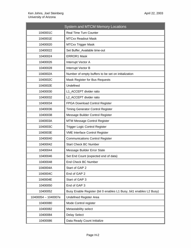
Ken Johns, Joel Steinberg April 22, 2003University of Arizona
Page H-2
System and MTCM Memory Locations
1040001C Real Time Turn Counter
1040001E MTCxx Readout Mask
10400020 MTCxx Trigger Mask
10400022 Set Buffer_Available time-out
10400024 ERROR1 Mask
10400026 Interrupt Vector A
10400028 Interrupt Vector B
1040002A Number of empty buffers to be set on initialization
1040002C Mask Register for Bus Requests
1040002E Undefined
10400030 L1_ACCEPT divider ratio
10400032 L2_ACCEPT divider ratio
10400034 FPGA Download Control Register
10400036 Timing Generator Control Register
10400038 Message Builder Control Register
1040003A MTM Message Control Register
1040003C Trigger Logic Control Register
1040003E VME Interface Control Register
10400040 Communications Control Register
10400042 Start Check BC Number
10400044 Message Builder Error State
10400046 Set End Count (expected end of data)
10400048 End Check BC Number
1040004A Start of GAP 2
1040004C End of GAP 2
1040004E Start of GAP 3
10400050 End of GAP 3
10400052 Busy Enable Register (bit 0 enables L1 Busy, bit1 enables L2 Busy)
10400054 – 1040007e Undefined Register Area
10400080 Mode Control register
10400082 Metastability select
10400084 Delay Select
10400086 Data Ready Count Initialize
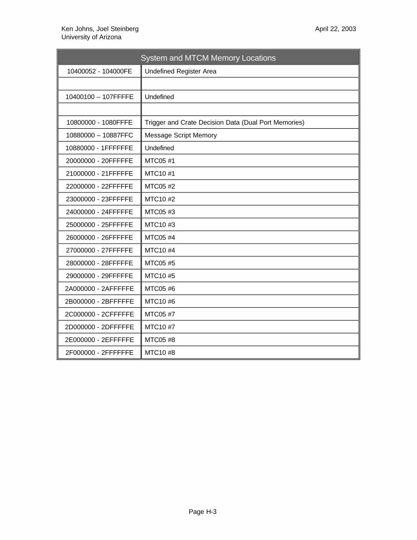
Ken Johns, Joel Steinberg April 22, 2003University of Arizona
Page H-3
System and MTCM Memory Locations
10400052 - 104000FE Undefined Register Area
10400100 – 107FFFFE Undefined
10800000 - 1080FFFE Trigger and Crate Decision Data (Dual Port Memories)
10880000 – 10887FFC Message Script Memory
10880000 - 1FFFFFFE Undefined
20000000 - 20FFFFFE MTC05 #1
21000000 - 21FFFFFE MTC10 #1
22000000 - 22FFFFFE MTC05 #2
23000000 - 23FFFFFE MTC10 #2
24000000 - 24FFFFFE MTC05 #3
25000000 - 25FFFFFE MTC10 #3
26000000 - 26FFFFFE MTC05 #4
27000000 - 27FFFFFE MTC10 #4
28000000 - 28FFFFFE MTC05 #5
29000000 - 29FFFFFE MTC10 #5
2A000000 - 2AFFFFFE MTC05 #6
2B000000 - 2BFFFFFE MTC10 #6
2C000000 - 2CFFFFFE MTC05 #7
2D000000 - 2DFFFFFE MTC10 #7
2E000000 - 2EFFFFFE MTC05 #8
2F000000 - 2FFFFFFE MTC10 #8

Ken Johns, Joel Steinberg April 22, 2003University of Arizona
Page H-4
MTCxx Memory Locations
Relative Address Description
000000 MTCxx Card Status Register
000002 MTCxx Card Error Register
000004 MTCxx Card Latched Error Register
000006 MTCxx Serial Error Register
000008 MTCxx Latched Serial Error Register
00000A Undefined
00000C Buffer Transfer FIFO (Read Only)
00000E Pending Transfer FIFO (Read Only)
000010 Test Data FIFO Control Register
000012 Test Data FIFO Data Input
000020 MTCxx Serial Input Mask Register
000022 Program ID for FPGA #1
000024 Program ID for FPGA #2
000026 Program ID for FPGA #3
000028 Program ID for FPGA #4
00002A Program ID for FPGA #5
00002C Program ID for FPGA #6
00002E Program ID for FPGA #7
000030 Program ID for FPGA #8
000032 Program ID for FPGA #9
000034 Program ID for FPGA #10
000036 Board Type ID and serial Number for MTCxx Flavor Board
000038 MTCxx Serial Number
00003A Checksum for FPGA #1
00003C Checksum for FPGA #2
00003E Checksum for FPGA #3
000040 Checksum for FPGA #4
000042 Checksum for FPGA #5
000044 Checksum for FPGA #6
000046 Checksum for FPGA #7
000048 Checksum for FPGA #8
00004A Checksum for FPGA #9
00004C Checksum for FPGA #10
00004E - 00FFE Undefined

Ken Johns, Joel Steinberg April 22, 2003University of Arizona
Page H-5
MTCxx Memory Locations
Relative Address Description
001000 - 001FFE Dual Port Ram
100000 - 1FFFFE Program Data for FPGAs

Ken Johns, Joel Steinberg April 22, 2003University of Arizona
Page I-1
Appendix I - Glossary
MTCM Muon Trigger Crate Manager - The MTCM forms regional trigger decisions from datareceived from MTCxx cards in the Muon Trigger Crate. The MTCM also receives timingand trigger information from the MRC.
MTC05 Muon Trigger Card type “05” - The Muon Trigger Card which uses tracks from the CFTtrigger and scintillator hit information.
MTC10 Muon Trigger Card type “10” - The Muon trigger Card which uses wire chamber hit andscintillator hit information.
MTCxx Muon Trigger Card type “xx” - Refers to both the MTC05 and MTC10 cards.
MTM Muon Trigger Manager - Receives regional trigger decisions from the three MTCM cardsand forms a global muon trigger decision which is sent to the Trigger framework.
TF Trigger Framework -
MRC Muon Readout Card - The MRC distributes timing and trigger information to the muonfront end cards and muon trigger cards. This information is typically sent to the cratemanager of these systems. The MRC also receives data from the muon front end cardsand muon trigger cards, termed L2 Data this data is read out from the mRC by the VBDfor use in the L3 Trigger.
VBD VME Branch Driver -
L1 Level 1 Trigger - The trigger has a 10 kHz accept rate and 4 µs processing time.
L2 Level 2 Trigger - The trigger has a 1 kHz accept rate and 100 µs processing time.
L3 Level 3 Trigger - The trigger has a 10 Hz accept rate and 25 ms processing time.
BC Bunch Crossing - There are 159 BC’s in one turn, each composed of 7 RF Clocks thatoperate at 53 MHz