Embed Size (px)
Citation preview

arX
iv:p
hysi
cs/0
5031
51 v
1 1
7 M
ar 2
005
Fermilab-PUB-05-034-E
The Muon System of the Run II DØ Detector
V.M. Abazovg, B.S. Acharyaf , G.D. Alexeevg, G. Alkhazovk,V.A. Anosovg, B. Baldinn, S. Banerjeef , O. Bardonr,
J.F. Bartlettn, M.A. Baturitskyg,u, D. Beutelo, V.A. Bezzubovj,V. Bodyagini, J.M. Butlerq, H. Ceasen, E. Chin, D. Denisovn(1),
S.P. Denisovj, H.T. Diehln, S. Doulasr, S.R. Dugadf ,O.V. Dvornikovg,v, A. Dyshkanto, M. Eadso, A. Evdokimovh,V.N. Evdokimovj, T. Fitzpatrickn, M. Fortnero, V. Gavrilovh,
Y. Gershteinm, V. Golovtsovk, R. Goodwinn,Yu.A. Gornushking, D.R. Greenn, A. Guptaf , S.N. Gurzhievj,
G. Gutierrezn, H. Haggertyn, P. Hanletr, S. Hansenn, E. Hazenq,D. Hedino, B. Hoeneisene, A.S. Iton, R. Jayantil, K. Johnsl,
N. Jouravlevg, A.M. Kalining, S.D. Kalmanif , Y.N. Kharzheevg,N. Kirschr, E.V. Komissarovg, V.M. Korablevj, A. Kostritskyj,
A.V. Kozelovj, M. Kozlovskyn, N.P. Kravchukg,M.R. Krishnaswamyf, N.A. Kuchinskyg, S. Kuleshovh,
A. Kupcod, M. Larwilln, R. Leitnerb, V.V. Lipaevj,A. Lobodenkok, M. Lokajicekd, H.J. Lubattit, E. Machadoq,
M. Maityq, V.L. Malyshevg, H.S. Maoa, M. Marcusr,T. Marshallp, A.A. Mayorovj, R. McCroskeyl, Y.P. Merekovg,V.A. Mikhailovg,u, N. Mokhovn, N.K. Mondalf , P. Nagarajf ,
V.S. Narasimhamf, A. Narayananl, P. Neustroevk,A.A. Nozdring, B. Oshinowon, N. Parasharr, N. Paruaf ,
V.M. Podstavkovn, P. Polozovh, S.Y. Porokhovoig,I.K. Prokhorovg, M.V.S. Raof , J. Raskowskio, L.V. Reddyf ,T. Regann, C. Rotolon, N.A. Russakovichg, B.M. Sabirovg,
B. Satyanarayanaf, Y. Scheglovk, A.A. Schukinj,H.C. Shankarf , A.A. Shishking, D. Shpakovr, M. Shupel,
V. Simakc, V. Sirotenkon, G. Smithn, K. Smolekc,K. Soustruznikb, A. Stefanikn, J. Steinbergl, V. Stolinh,D.A. Stoyanovaj, L. Stutten, J. Templel, N. Terentyevk,
V.V. Tetering, V.V. Tokmening, D. Tompkinsl, L. Uvarovk,S. Uvarovk, I.A. Vasilyevj, L.S. Vertogradovg,
P.R. Vishwanathf , A. Vorobyovk, V.B. Vysotskyg,w,H. Willutzkis, M. Wobischn, D.R. Woodr, R. Yamadan,
Preprint submitted to Elsevier Science 24 May 2006

Y.A. Yatsunenkog, F. Yoffen, M. Zanabrian, T. Zhaot,D. Zieminskap, A. Zieminskip, S.A. Zvyagintsevj 1
aInstitute of High Energy Physics, Beijing, People’s Republic of China
bCenter for Particle Physics, Charles University, Prague, Czech Republic
cCzech Technical University, Prague, Czech Republic
dInstitute of Physics, Academy of Sciences, Center for Particle Physics, Prague,
Czech Republic
eUniversidad San Francisco de Quito, Quito, Ecuador
fTata Institute of Fundamental Research, Mumbai, India
gJoint Institute for Nuclear Research, Dubna, Russia
hInstitute for Theoretical and Experimental Physics, Moscow, Russia
iMoscow State University, Moscow, Russia
jInstitute for High Energy Physics, Protvino, Russia
kPetersburg Nuclear Physics Institute, St. Petersburg, Russia
lUniversity of Arizona, Tucson, Arizona 85721
mFlorida State University, Tallahassee, Florida 32306
nFermi National Accelerator Laboratory, Batavia, Illinois 60510
oNorthern Illinois University, DeKalb, Illinois 60115
pIndiana University, Bloomington, Indiana 47405
qBoston University, Boston, Massachusetts 02215
rNortheastern University, Boston, Massachusetts 02115
sBrookhaven National Laboratory, Upton, New York 11973
tUniversity of Washington, Seattle, Washington 98195
u Visitors from Institute of Nuclear Problems of the Belarusian State University,
Minsk, Belarus
v Visitor from National Scientific and Educational Centre of Particle and High
Energy Physics, Belarusian State University, Minsk, Belarus
w Visitor from Research and Production Corporation ”Integral”, Minsk, Belarus
2

Abstract
We describe the design, construction and performance of the upgraded DØ muonsystem for Run II of the Fermilab Tevatron collider. Significant improvements havebeen made to the major subsystems of the DØ muon detector: trigger scintillationcounters, tracking detectors, and electronics. The Run II central muon detector has anew scintillation counter system inside the iron toroid and an improved scintillationcounter system outside the iron toroid. In the forward region, new scintillationcounter and tracking systems have been installed. Extensive shielding has beenadded in the forward region. A large fraction of the muon system electronics is alsonew.
1 Corresponding author. Tel.: + 630-840-3851; Fax: + 630-840-8886; E-mail ad-
dress: [email protected]
3

1 Introduction
The DØ detector [1] collected approximately 120 pb−1 of data during Run I ofthe Fermilab Tevatron collider from 1992 to 1996. While the Tevatron was shutdown for improvements from 1996 to the beginning of Run II in 2001, the DØcollaboration undertook and completed a substantial detector modificationprogram in order to exploit fully the potential of the upgraded Fermilab col-lider including an increase in instantaneous luminosity up to 3×1032 cm−2s−1,an increase in center of mass energy from 1.8 to 1.96 TeV, and a reduction inbunch spacing from 3.5 µs to 396 ns. With improvements to the Tevatron, weexpect to collect 4−8 fb−1 of data by the end of Run II in 2009. In this paperwe describe the design, construction and performance of the DØ Run II muonsystem.
The muon system of a general-purpose collider detector should provide efficientmuon triggering and identification with extensive solid angle and momentumcoverage and low backgrounds. Stable and reliable performance over manyyears of operation and radiation hardness in the high luminosity hadron col-lider environment are critical for the muon system as well. The Run II DØmuon system was designed with the above goals in mind while also taking intoaccount existing technical constraints of the Run I detector [2] and availableresources.
The main components of the DØ muon system are identified in the cross-sectional view of the Run II DØ detector shown in Fig. 1. The DØ coordinatesystem has the z -axis along the Tevatron proton beam direction, x -axis hori-zontal and pointing out of the Tevatron ring, and y-axis pointing straight up.The center of the coordinate system is located in the central tracking detec-tor center. We use pseudorapidity defined as η = − ln[tan(θ/2)], where θ isthe polar angle measured relative to the z -axis. The Run I DØ muon system[2] consisted of two subsystems: the Wide Angle MUon System (WAMUS)and the Small Angle MUon System (SAMUS). WAMUS, covering the pseu-dorapidity region |η| < 2.0, consisted of proportional drift tubes (PDTs) andthree large iron toroidal magnets: a central toroid (CF) and two end toroids(EFs). The PDT chambers were arranged in three layers: the A-layer insidethe toroids and the B and C-layers outside the toroids. SAMUS, covering 2.0< |η| < 3.0, consisted of a set of drift tube planes and two small iron toroids.For Run II, the PDT chambers in the forward region (1.0 < |η| < 2.0) werereplaced by a new tracking system and the SAMUS magnets were replaced byshielding assemblies. The three main toroids in the DØ muon magnet system,the CF and the two EFs, were not changed. The Run II DØ muon magnetsystem is discussed in Section 2.
Simulation studies and experience from Run I demonstrated that additional
4

Fig. 1. Cross-sectional view of the DØ Run II detector.
shielding was needed to protect the muon system and other components ofthe DØ detector from the increased background expected in Run II. Twosets of shielding assemblies consisting of layers of iron, polyethylene and leadwere installed in the existing apertures of the end iron toroids and aroundthe accelerator quadrupole magnets. The design of the new shielding systemis discussed in Section 3.
In Section 4 we discuss three scintillation counter systems added to the orig-inal DØ detector. Triggering on muons and identifying them in the Run IIenvironment with shortened bunch spacing and increased luminosity requiresthe use of scintillation counters with fine segmentation and good time res-olution. The effort to improve the muon trigger began in the latter part ofRun I when 240 scintillation counters covering the region |η| < 1.0 and six ofthe eight octants in azimuth were installed. The solid angle coverage of thesecounters has now been extended to the bottom of the detector with the instal-lation of 132 additional counters. This counter system is discussed in Section4.1. In addition to the counters outside of the central iron toroid, two newscintillation trigger counter systems have been added for Run II: a set of 630scintillation counters called Aϕ counters are located inside the central toroid
5

and another 4214 counters called “pixel” counters are installed in the forwardregion (1.0 < |η| < 2.0) [3]. The Aϕ counter system is discussed in Section 4.2and the pixel counter system is discussed in Section 4.3.
In Section 5 we describe the muon tracking detector which consists of PDTsin the central rapidity region |η| < 1.0 and mini drift tubes (MDTs) in theforward region (1.0 < |η| < 2.0). The MDT system is a new tracking systemthat replaces the WAMUS PDT chambers in the forward region.
In Section 6 we discuss the electronics design of the DØ muon system, describemethods of electronics synchronization to the accelerator, and present theparameters of the major electronics modules designed for Run II. A summaryis given in Section 7.
2 Muon toroidal magnets
The three magnets of the Run II muon detector magnet system [4]; the centraliron toroid and the two end iron toroids; are mounted on the platform thatmoves the entire detector between detector assembly hall and the collisionhall. These toroids account for about 65% of the total 5500 ton weight of thedetector. A cross-sectional view of the Run II DØ magnet system is presentedin Fig. 2. End views of the CF and EF magnets are shown in Fig. 3. Two smalltoroids that were located inside the square apertures of the two end toroidsas part of SAMUS in Run I were removed and replaced by two shieldingassemblies that are discussed in the next section.
As indicated in the end view of the CF toroid in Fig. 3, the CF toroid yokeis made of two side pieces of steel plus a central segment at the bottom. Theseparating lines of the three pieces are indicated by the thick solid vertical lines(one at the top and two at the bottom of the sketch of the CF). The centralsegment of the CF is mounted on the detector platform. The calorimeter, thesuperconducting solenoid, and the central tracking systems are supported bythis central segment. The two side toroid segments move laterally when thedetector is opened to permit access to the inner detector systems. Stainlesssteel shim plates, 0.48 cm thick at the top parting line and 0.32 cm thick at thetwo bottom parting lines, prevent the three magnet elements from “bonding”together magnetically due to residual induction in the steel. Penetrations areprovided through the lower sections of the CF yoke for the passage of thecables of the tracking system. The yokes of the EFs are made of steel withcentral openings.
The central toroid has twenty coils; each end toroid has eight coils. Each CFcoil has ten turns and each EF coil has eight turns. All coils in the toroidal
6
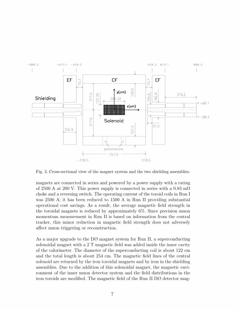
Fig. 2. Cross-sectional view of the magnet system and the two shielding assemblies.
magnets are connected in series and powered by a power supply with a ratingof 2500 A at 200 V. This power supply is connected in series with a 0.83 mΩchoke and a reversing switch. The operating current of the toroid coils in Run Iwas 2500 A; it has been reduced to 1500 A in Run II providing substantialoperational cost savings. As a result, the average magnetic field strength inthe toroidal magnets is reduced by approximately 6%. Since precision muonmomentum measurement in Run II is based on information from the centraltracker, this minor reduction in magnetic field strength does not adverselyaffect muon triggering or reconstruction.
As a major upgrade to the DØ magnet system for Run II, a superconductingsolenoidal magnet with a 2 T magnetic field was added inside the inner cavityof the calorimeter. The diameter of the superconducting coil is about 122 cmand the total length is about 254 cm. The magnetic field lines of the centralsolenoid are returned by the iron toroidal magnets and by iron in the shieldingassemblies. Due to the addition of this solenoidal magnet, the magnetic envi-ronment of the inner muon detector system and the field distributions in theiron toroids are modified. The magnetic field of the Run II DØ detector mag-
7

Fig. 3. a) End view of the CF magnet; b) End view of the EF magnet. The hole atx = −33 cm, y = 206.9 cm is for bypass of the Run I accelerator beam pipe.
net system is calculated using the program TOSCA [5] and corrected usingmeasured values of the field in the steel of the toroids. The estimated errorsof the field map are 1% for the iron magnets and 0.1% for the solenoid. Themagnetic field associated with the solenoidal magnet is shown in Fig. 4. Themagnetic field inside the CF and EF yokes is shown in Figs. 5 and 6.
Both toroidal and solenoidal magnets have current reversing switches whichare reversed regularly so that the experiment collects approximately equalamounts of data in each of the four possible field configurations.
3 Backgrounds and Shielding
Studies performed during Run I led us to understand that most hits in theRun I muon detectors did not originate from colliding-beam-produced muons.Rather, there were several sources of particles that accounted for the highdetector occupancies observed. First, associated with proton and antiprotonbeams losses in the Tevatron and their subsequent interaction with the ac-celerator components, there was a background of particles coming from theaccelerator tunnel into the DØ collision hall. To suppress this background,two protective measures have been developed based on MARS [6] calculations
8

-400
-200
0
200
400
-400 -200 0 200 400
y (c
m)
z (cm)
Toroid
Solenoid
21.78
12.84
21.78
20.12
20.00
20.12
21.80
12.85
21.80
1.00
0.65
0.32
0.25 .63 .39 .30 0.29 0.24 0.25
0.16
0.18
0.370.450.340.330.450.41
0.19
0.20
0.15
0.200.220.24.24.210.08
0.32
0.65
1.00
Fig. 4. Solenoid magnetic field in the y − z plane of the detector. The magnetic fieldis in kG.
and implemented during the 1994 Tevatron shutdown [7]: (i) two 2-m-thickconcrete walls were installed in the tunnel on both sides of the DØ collisionhall; (ii) the accelerator A0 scraper was replaced with a new one with two thinscattering targets. After these steps, the Tevatron halo backgrounds becamenegligible compared to other backgrounds [7,8]. Second, the remnants of theproton and antiproton, after their collision at the interaction point, interactwith the beam pipe, the edges of the forward calorimeter near the beam pipe,and the accelerator’s low-beta quadrupole magnets. The background from theforward calorimeter edges was seen in all muon detector components insidethe toroid, including the central muon detectors. The time spectrum of theseparticles was measured with scintillation counters. The arrival time was as ex-pected for particles originating near the beam pipe at the calorimeter edges.Because the path was longer than that of muons originating from collisions,the background particles arrive measurably later than muons originating in
9

Fig. 5. Magnetic field in the central toroid magnet. The magnetic field is in kG.
the detector center. The background from the low-beta quadrupole magnetswas detected in all parts of the forward muon detector and in those parts ofthe central muon system not protected by the EF magnets. Cosmic ray muonsare only a small contributor to the detectors’ occupancy.
In response to the experience in Run I, we have performed a detailed analysisof shielding for the Run II muon detector [8,9]. Simulations were performedwith GEANT [10] and MARS Monte Carlo codes. The new shielding designincludes two 100-ton assemblies surrounding the beam pipe and the low-betaquadrupole magnets on both ends of the detector. The shielding assemblyextends from the end of the calorimeter to the wall of the collision hall. Topermit articulation of the detector during opening and roll-in, each of thetwo shielding assemblies is made in three overlapping segments. Fig. 7 showsa shielding assembly in the detector operating position. During the detector
10

-400
-200
0
200
400
-400 -200 0 200 400
Fig. 6. Magnetic field in the end toroid magnet. The magnetic field is in kG.
opening process, the end section of the shielding assembly is first split openand the middle section is moved away from detector center on its support rails.The front section of the shielding assembly is supported by the EF toroid andmoves together with the EF toroid.
The shielding assemblies consist of layers of iron, polyethylene, and lead. Theinnermost layer is made of iron because it has reasonably short interaction(16.8 cm) and radiation (1.76 cm) lengths, and is relatively inexpensive. Theoptimal thickness of the individual layers is determined by Monte Carlo simu-lations (GEANT and MARS). The iron absorbs electromagnetic and hadronicshowers that make up the majority of the background. However, iron is al-most transparent to low energy neutrons. Polyethylene is used as a neutronabsorber because it is rich in hydrogen and effective in moderating neutrons.Neutron capture in the polyethylene results in gamma rays. They are, in turn,
11

Fig. 7. Shielding assembly.
absorbed by the outermost lead layer. The shielding is a square tube with wallthickness of 51 cm of iron followed by 15 cm of polyethylene and 5 cm of lead.
The comparison between simulated energy depositions from hadron and elec-tromagnetic showers at an instantaneous luminosity of 2×1032 cm−2s−1 can beseen in Figs. 8 and 9. Fig. 8 shows the muon system without and Fig. 9 with theshielding system. The three scintillation counter layers in the detector forwardregion (seen as vertical lines in the figures) are located approximately 400, 690and 830 cm from the interaction region. The grayscale of the detector areasindicates the level of the radiation dose. Using the Monte Carlo simulation,we find that the energy deposition in the scintillator planes is reduced by afactor of approximately 102. As a result, the number of background hits in themuon counters is reduced by a factor of between 40 and 102 [8,9]. Backgroundrates obtained during Run II agree with the Monte Carlo simulation within50%. For example, occupancy of the B and C-layers of the forward triggerscintillation counters (Section 4.3) for minimum bias event at a luminosity of2×1031 cm−2s−1 is 0.02%.
12

Fig. 8. Energy depositions from hadron (top) and electromagnetic showers (bottom)in the DØ muon detector without the shielding system. The units of the energydeposition scale shown on the right side of the figure are GeV/cm3 per sec for aninstantaneous luminosity of 2×1032 cm−2s−1. The darker shades indicate higherenergy deposition. Vertical axis is y and horizontal axis is z coordinate in the DØcoordinate system given in cm.
4 Scintillation trigger counters
The triggering capability of the Run II DØ muon system has been greatlyenhanced by the addition of scintillation counters with fine segmentation andgood time resolution. The central region (|η| < 1.0) of the Run II DØ detectoris covered by two layers of scintillation counters, one layer outside of the centraltoroid and one layer inside. The forward regions (1.0 < |η| < 2.0) are coveredby three layers of scintillation counters, one layer inside the end toroid andtwo layers outside. These counters are used to trigger on muons associated
13
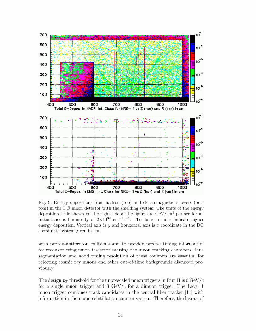
Fig. 9. Energy depositions from hadron (top) and electromagnetic showers (bot-tom) in the DØ muon detector with the shielding system. The units of the energydeposition scale shown on the right side of the figure are GeV/cm3 per sec for aninstantaneous luminosity of 2×1032 cm−2s−1. The darker shades indicate higherenergy deposition. Vertical axis is y and horizontal axis is z coordinate in the DØcoordinate system given in cm.
with proton-antiproton collisions and to provide precise timing informationfor reconstructing muon trajectories using the muon tracking chambers. Finesegmentation and good timing resolution of these counters are essential forrejecting cosmic ray muons and other out-of-time backgrounds discussed pre-viously.
The design pT threshold for the unprescaled muon triggers in Run II is 6 GeV/cfor a single muon trigger and 3 GeV/c for a dimuon trigger. The Level 1muon trigger combines track candidates in the central fiber tracker [11] withinformation in the muon scintillation counter system. Therefore, the layout of
14

the scintillation counters is required to match the 4.5 trigger segmentationin ϕ of the fiber tracker. More information about the DØ three-level triggersystem is given in Section 6.
4.1 Scintillation counters outside the central toroid
During the latter part of Run I, 240 scintillation counters for muon triggeringwere installed on the top and two sides of the C-layer PDT chambers. Detailsof this counter system are given in Ref. [12]. These scintillation counters span|η| < 1.0 and cover six octants (top and sides) in azimuth.
For Run II, an additional 132 scintillation counters covering the two bottomoctants were installed under the central toroid and the two end toroids. Thedesign of these counters is similar to the counters installed previously. They aremade of scintillator sheets with embedded wavelength shifting (WLS) fibersfor light collection. EMI 9902K [13] photomultiplier tubes 38 mm in diameterare used to read out the light produced by the counters. The size of thesecounters is approximately 200 cm × 40 cm. They are arranged in two layers(B and C) and are oriented with the short dimension (40 cm) along the ϕdirection, so that each counter covers approximately 4.5 in ϕ.
4.2 Aϕ scintillation counters inside the central toroid
The Aϕ counter system added for Run II has 630 counters mounted on the A-layer PDT chambers between the central iron toroid and the calorimeter cov-ering |η| < 1.0. Each counter approximately matches the 4.5 ϕ-segmentationof the central fiber tracker. There are nine counter barrels located within−1.0 < η < 1.0. Combining the “in-time” hits from the Aϕ counters withtracks in the central fiber tracker is a key element of muon triggers with lowpT thresholds. The time gate for Aϕ counters signals is 24 ns at the Level 1trigger. In addition, the Aϕ counters provide timestamps to reconstruct muontracks in the A-layer PDT chambers. This is particularly important for low-pT
muons that do not penetrate the toroidal magnet.
4.2.1 Counter design
The Aϕ counters are made from 12.7-mm-thick BICRON 404A scintillatorwith BICRON BCF 92 wavelength shifter fiber [14] embedded in machinedgrooves [15] (see Fig. 10). This WLS has a fast (2.7 ns) decay time and itsabsorption spectrum matches the 420 nm emission peak of the 404A scintil-lator. The grooves are machined 4.5 cm apart and 6 mm deep and run from
15

Fig. 10. Top and side views of an Aϕ counter and counter cross section.
the center of the counter to its edge. Six individual fibers are glued into eachgroove and tapered out of the groove at the middle of the counter. Fibersfrom 10 to 16 grooves are combined into a single bundle that directs lightto a 25-mm-diameter green-extended 115M phototube made by MELZ [16].This phototube has an average quantum efficiency of 15% at 500 nm with amaximum gain around 106. The sensitivity peak of the 115M photocathodematches the 480 nm emission peak of the WLS fibers. The phototube is se-cured to the counter case at the center of the counter. All fibers are within5 mm of being the same length. Each counter is wrapped in a layer of TYVEK[17] type 1056D sheet with a layer of black TEDLAR [17] over the TYVEKfor light-tightness. The counter case is an aluminium box with welded corners.The light-tight case provides mechanical protection for the counter, supportsthe PMT assembly, and provides counter mounts.
The Aϕ counters operate in the 200 to 350 G residual magnetic field of themuon toroidal and central solenoidal magnets. Studies of magnetic shieldinghave been performed [18] with the goal of reducing the magnetic field in thephototube region to about 1 G, which is necessary for high gain operation. Theshielding consists of a 6-mm-thick soft steel tube and a 1.2-mm-thick µ-metal
16

Table 1Numbers and sizes of Aϕ counters.
Number Length (cm) Width (cm)
216 84.5 36.7
144 84.5 27.5
270 84.5 23.1
Table 2Segmentation of the Aϕ counters in a quadrant.
Counter Top Side Bottom
Width (cm) quadrant quadrants quadrant
36.7 3 3 3
27.5 1 3 1
23.1 12 8 2
27.5 1 3 1
36.7 3 3 3
Total number 9 × 20 2 × 9 × 20 9 × 10
cylinder. With this shielding, the phototubes can operate without significantgain reduction in a 700 G magnetic field perpendicular to the phototube axis.For fields parallel to the tube axis, the gain reduction is less than 5% at 250 Gand less than 10% at 350 G.
4.2.2 Counter arrangement and mounting
The Aϕ counters cover the four quadrants of the A-layer PDT chambers.The length of the A-layer PDT chambers in the beam direction is approxi-mately 7.6 m. Nine barrels of counters cover the entire span |η| < 1.0 in thebeam direction. The length of each Aϕ counter is 84.5 cm. Twenty countercolumns, of three different widths, cover one quadrant in the azimuthal di-rection. Three different widths; large, medium and small; allow each columnof counters to cover approximately 4.5 in ϕ, matching the ϕ-segmentation ofthe fiber tracker trigger. The numbers and dimensions of the three differentlysized counters are given in Table 1. Fig. 11 shows the counter arrangement ina quadrant and Table 2 summarizes the counters’ segmentation.
The edges between neighboring counters in azimuth overlap to prevent in-efficiency. The average overlap between counters is about 3% of the counterwidth. In the longitudinal direction, the counters are mounted end-to-end witha 10 mm gap between scintillators. The bottom quadrant is instrumented with
17
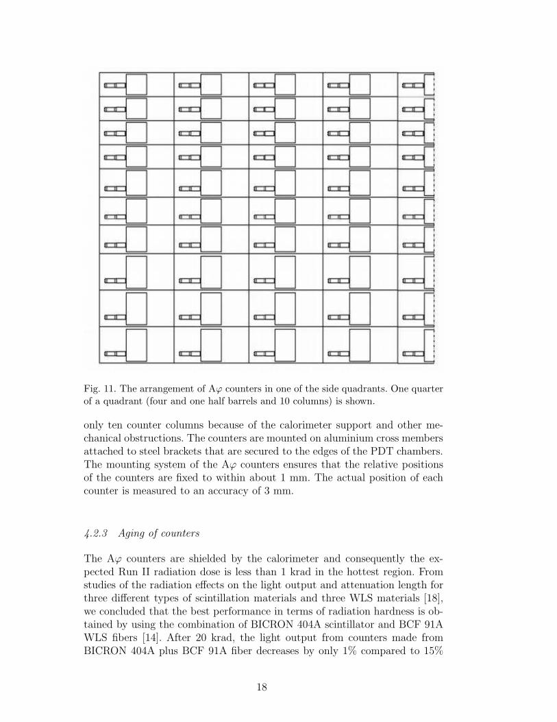
Fig. 11. The arrangement of Aϕ counters in one of the side quadrants. One quarterof a quadrant (four and one half barrels and 10 columns) is shown.
only ten counter columns because of the calorimeter support and other me-chanical obstructions. The counters are mounted on aluminium cross membersattached to steel brackets that are secured to the edges of the PDT chambers.The mounting system of the Aϕ counters ensures that the relative positionsof the counters are fixed to within about 1 mm. The actual position of eachcounter is measured to an accuracy of 3 mm.
4.2.3 Aging of counters
The Aϕ counters are shielded by the calorimeter and consequently the ex-pected Run II radiation dose is less than 1 krad in the hottest region. Fromstudies of the radiation effects on the light output and attenuation length forthree different types of scintillation materials and three WLS materials [18],we concluded that the best performance in terms of radiation hardness is ob-tained by using the combination of BICRON 404A scintillator and BCF 91AWLS fibers [14]. After 20 krad, the light output from counters made fromBICRON 404A plus BCF 91A fiber decreases by only 1% compared to 15%
18

for a counter that uses BCF 92 fiber. This is caused mainly by the decreasedattenuation length in the WLS fibers due to radiation damage. Since the ex-pected dose is less than 1 krad in the highest dose location (for total deliveredluminosity of 10 fb−1), BCF 92 fibers were selected for better light output andtiming. We expect no significant performance degradation of Aϕ counters inRun II due to radiation damage.
The effect of phototube aging is also expected to be small. The gain reductionof phototubes after 100 C charge deposition on the phototube anode is about10%. The charge deposition for the phototubes in the Aϕ counters is expectedto be well below 100 C. Any small gain reduction can be compensated for byadjusting the signal discrimination threshold or phototube operating voltage.
4.2.4 Counter performance
During prototype counter tests the average integrated pulse height was mea-sured to be approximately 55 photoelectrons for cosmic ray muons that pen-etrate the middle of the counter. The measured reduction of signal amplitudefor the area that is farthest away from the phototube is approximately 7%. Thetime resolution of the counter is measured to be 0.8 ns, for 20 mV discrimina-tion threshold, while muon signal amplitude is adjusted to be approximately0.10 V.
During counters production, the light yield for each scintillation counter wasmeasured using cosmic muons and the gain of each phototube was measuredon a test stand. Phototube-to-counter matching was then done to obtain thesame signal amplitudes in each group of fifteen counters connected to the samehigh voltage power supply during detector operation.
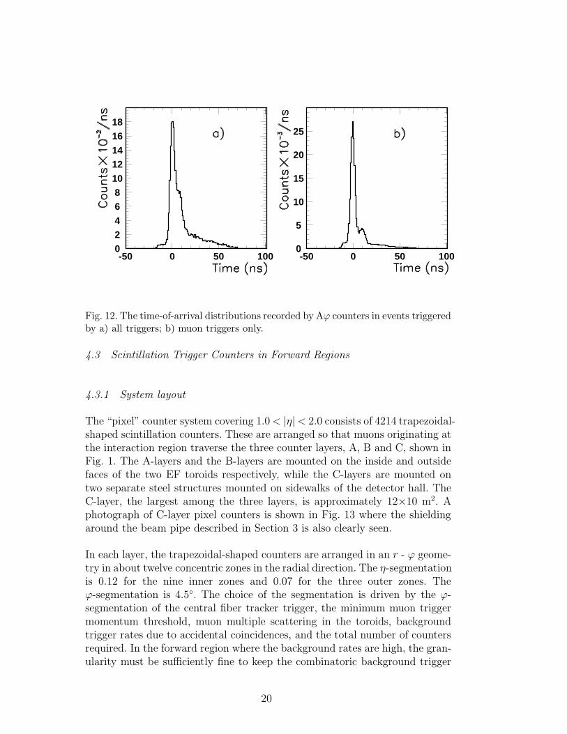
The performance of the installed Aϕ counter system during Run II has beenmonitored using muons from proton-antiproton collisions. The time-of-arrivalof hits using all DØ triggers is shown in Fig. 12a and the time-of-arrival of hitsusing muon triggers based on the central scintillation counters only is shownin Fig. 12b. The peaks around zero in both figures are from muons originatingat the interaction region. The time-of-arrival distribution shown in Fig. 12aincludes a significant number of late hits from the various background sourcesdiscussed in Section 3. A secondary peak near 10 ns that is visible in Fig. 12b iscaused by backscattered particles from the edges of calorimeter. The time res-olution of all 630 Aϕ counters combined is σt = 2.5 ns without corrections fordifferences in time-of-flight, light propagation in the counters or cable lengthwithin each group of fifteen counters. Other factors that contribute to themeasured time resolution of the Aϕ counters include the intrinsic resolutionof the counter and variations in the z -position of the interaction vertex.
19
024681012141618
-50 0 50 1000
5
10
15
20
25
-50 0 50 100
Fig. 12. The time-of-arrival distributions recorded by Aϕ counters in events triggeredby a) all triggers; b) muon triggers only.
4.3 Scintillation Trigger Counters in Forward Regions
4.3.1 System layout
The “pixel” counter system covering 1.0 < |η|< 2.0 consists of 4214 trapezoidal-shaped scintillation counters. These are arranged so that muons originating atthe interaction region traverse the three counter layers, A, B and C, shown inFig. 1. The A-layers and the B-layers are mounted on the inside and outsidefaces of the two EF toroids respectively, while the C-layers are mounted ontwo separate steel structures mounted on sidewalks of the detector hall. TheC-layer, the largest among the three layers, is approximately 12×10 m2. Aphotograph of C-layer pixel counters is shown in Fig. 13 where the shieldingaround the beam pipe described in Section 3 is also clearly seen.
In each layer, the trapezoidal-shaped counters are arranged in an r - ϕ geome-try in about twelve concentric zones in the radial direction. The η-segmentationis 0.12 for the nine inner zones and 0.07 for the three outer zones. Theϕ-segmentation is 4.5. The choice of the segmentation is driven by the ϕ-segmentation of the central fiber tracker trigger, the minimum muon triggermomentum threshold, muon multiple scattering in the toroids, backgroundtrigger rates due to accidental coincidences, and the total number of countersrequired. In the forward region where the background rates are high, the gran-ularity must be sufficiently fine to keep the combinatoric background trigger
20

Fig. 13. A photograph of C-layer pixel counters.
rate low. For three layers of N counters, the combinatoric background rejec-tion scales as N 3 assuming hits in the layers are uncorrelated, so small changesin granularity have a big effect on the combinatoric background.
The size of the smallest counters in the A-layer is 9×14 cm2 and the size ofthe largest counters in the C-layer is 60×110 cm2. The minimum size of thepixel counters is defined by the 3 multiple scattering angular spread of apT = 3 GeV/c muon through the end toroid. As mentioned earlier, triggeringon muons down to pT = 3 GeV/c is one of the basic requirements for the DØmuon trigger system.
4.3.2 Pixel counter design and mounting
Several light collection methods were studied in order to optimize the pixelcounters for light yield, uniformity, time resolution, and background rejectionwhile maintaining a reasonable production cost. From measurements [15], weconcluded that for the geometry of our counters, WLS bars give better lightcollection efficiency and allow a simpler construction procedure than WLSfibers. The design using WLS bars for light collection was chosen as the basicoption for the large majority of the counters [18].
21

The counters use Kumarin 30 type WLS bars [19] for light collection and 12.7-mm-thick BICRON 404A scintillator plates of trapezoidal shape. BICRON404A scintillation light emission peak is 420 nm, its decay time is 2.0 ns, andits attenuation length is 1.7 m. The absorption peak of the Kumarin 30 WLSbar matches the emission peak of the scintillator. The light emission peakof the Kumarin 30 WLS bar is 480 nm, the decay time is 2.7 ns, and theattenuation length is 1.4 m.
Effects of radiation damage on the light output of Kumarin 30 WLS bars andBICRON 404A scintillator were studied using sample counters of differentsizes [18]. We concluded that the expected integrated Run II radiation levelof 1 krad for an integrated luminosity of 10 fb−1 is significantly below whatwould degrade pixel counter performance.
Fig. 14 shows the details of the counter design. All four sides of the trapezoidalscintillator plate are machined but not polished. Our studies concluded thatthe less expensive unpolished design has better photoelectron yield and uni-formity [15,18]. Two WLS bars, 4.2 mm thick and 12.7 mm wide, are placedalong two edges of the scintillator plate with air gaps provided by narrowstrips of adhesive tape attached to the scintillator plate as spacers. The endsections of both bars are bent by 44 to deliver light to the 25-mm-diameterMELZ 115M phototube [16]. The opposite ends of bars are made reflectiveusing aluminized Mylar tape. To provide light tightness, the scintillator andWLS bars are wrapped in a layer of TYVEK material [17] (type 1056D) andtwo layers of black paper. The wrapped counter assembly is secured in a boxmade of two aluminium plates and an extruded aluminium profile along theperimeter.
A different light collection design was used for approximately 150 counterslocated in cramped areas. These counters have twelve WLS fibers along theedges of 12.7-mm-thick Bicron 404A scintillator plates for collecting the scin-tillation light. These fibers are BCF 92 multiclad fibers [14]. Both ends of thefibers are glued into plexiglass light-collector tubes, polished, and brought toa MELZ 115M phototube located on top of the counter assembly. This designprovides 60 to 110 photoelectrons per minimum ionizing particle, dependingon the counter’s size. Using multiclad instead of singleclad BCF 92 fiber [15]increases the light yield 1.4 and 1.7 times for counter sizes 13×18 cm2 and38×44 cm2, respectively.
A phototube assembly; containing a phototube, magnetic shielding, and tubebase; is attached to the counter case by a threaded connection. The residualmagnetic field of the muon toroids and the central solenoidal magnet is typi-cally 150 G for A-layer pixel counters but can reach 300 G in some locations.For the B-layer pixel counters, the typical value is 100 G. The phototube mag-netic shielding is similar to the shielding used for the phototubes of the Aϕ
22

Fig. 14. The design of a pixel scintillation counter. Dimensions are given in mm.
counters. A resistive phototube base optimized for high gain and high timeresolution is mounted at the end of the phototube.
The counters are installed on the frames using a “fish scale” design as shownin Fig. 15. On the flat support frame, counters are tilted and supported byaluminium mounting brackets to achieve gapless coverage. All four edges ofa counter overlap with the edges of neighboring counters. This novel designmakes the procedure for assembling the pixel counter octants straightforwardand also made access to phototubes easy. Eight octants are assembled into a
23

Fig. 15. Fish scale design of the pixel counter mounting: a) counters arrangement;b) an aluminium mounting bracket.
pixel counter layer in the DØ assembly hall and then a complete pixel counterlayer is mounted on the detector as shown in Fig. 13. Placement accuracyof the octants is 3 mm and location of each layer is surveyed using opticalmethods to 1 mm accuracy. After parts of the DØ detector are moved toprovide access for service or repairs, the location of moved pixel counter layersis resurveyed with 1 mm precision.
4.3.3 Pixel counter performance
Performance studies have been done at the Fermilab 125 GeV/c test beamusing prototype counters with WLS bar readout. Three different sizes; large(60×106 cm2), typical (24×34 cm2), and small (17×24 cm2); were tested. Themeasured efficiencies and time resolutions shown in Fig. 16 indicate that thepixel counters’ peak efficiency is greater than 99.9% and the time resolution,depending on counter size, ranges from 0.5 ns to 1 ns. The average lightyield for 125 GeV/c pions was measured to be 60 photoelectrons for the largecounter and 184 for the small counter.
The production procedure for pixel counters included tests to check size tol-erances and light yield measurements using a 60Co radioactive source. Somecounters of each size have been tested using cosmic ray muons to calibrateradioactive source measurements to the number of photoelectrons. Accordingto the cosmic test, the number of photoelectrons varies from 240 for smallA-layer counters to 70 for the largest C-layer counters. The uniformity of lightcollection for particles irradiating the full surface of the counters is ±10%.
24

Fig. 16. Efficiency and time resolution of pixel counters. Open signs represent effi-ciency, closed signs time resolution.
Phototube-to-counter matching has been performed to get close signal ampli-tudes for each counter connected to the same high voltage power supply ina group of sixteen. This matching included the use of phototube test standresults obtained using LED and 60Co measurements. A final matching checkwas made by pulse height measurements using a 90Sr beta source. The uni-formity of 90Sr amplitudes for groups of sixteen counters achieved using thematching procedure is ±25% (full width). High voltage values selected duringthe matching process are used for Run II data taking. Uniformity in signalamplitudes as well as a reasonable choice of discriminator thresholds are il-lustrated in Fig. 17. This figure shows the amplitude distribution for recon-structed muons from proton-antiproton collisions for all 4214 counters. Thediscriminator threshold is equal to 7 mV or about 25 ADC channels.
Time distributions of pixel counters hits during proton-antiproton collisionsrun are shown in Fig. 18. The time distribution of muon hits originating in thecollision region peaks at zero. The time distribution of events selected witha minimum bias trigger, Fig. 18a, has a broad peak that ranges from zero to
25

0
200
400
600
800
1000
0 50 100 150 200 250 300 350 400 450 500
Fig. 17. Muon pulse height distribution for all 4214 pixel counters.
about 70 ns, mainly due to the late-arriving background particles discussedin Section 3. Hits in the 30 ns time gate are sent to the Level 1 trigger. Thedistribution obtained for events selected with a Level 1 muon trigger, Fig. 18b,shows a peak at zero with some background remaining. The time distributionfor hits from reconstructed muon tracks, Fig. 18c, has a clean peak at zerowith a time resolution of all counters combined σt = 2.2 ns. These resultsdemonstrate the power of the DØ forward muon trigger counters for selectingmuons in high rate proton-antiproton collisions. In DØ, about 50% of Level 1forward muon triggered events have a muon reconstructed off-line. Additionalrejection from the Level 2 trigger provides the capability of recording forwardmuon data sample with 80% purity and efficiency of about 90%.
Pixel counters are demonstrating stable operation and high reliability duringphysics data collection. Figure 19 shows the change in timing of 4214 countersin a one year interval measured by the LED calibration system (see Section
26

0
5
10
15
20
0 50 1000
4
8
12
16
20
24
28
0 50 1000
2
4
6
8
10
12
14
16
0 50 100
Fig. 18. Time spectra of hits recorded by pixel counters: a) minimum bias trigger;b) muon trigger; c) reconstructed muons.
4.5). Timing is stable within 0.5 ns for all 4214 counters. The stability of thecounter amplitudes is also measured by the LED pulser system. We foundthat amplitude stability is about 10% for individual counters in three years ofoperation. The stability of the signal amplitude, averaged over all phototubes,is better than 1%.
About fifteen counters have failed over three years of operation primarily dueto bad connectors and bases. Long-enough access to the collision hall to repairfailed counters occurs every 3−6 months. Movers designed to roll out fullyassembled A and B-layers of the pixel counters to provide access to all detectorparts for repairs are mounted on the top of the layers. The typical duration ofopening/closing a pixel counter layer including repairs is one day. The typicalnumber of non-working counters during physics data taking is about two or0.05%.
4.4 High voltage and readout electronics for scintillation counters
A total of 46 negative high voltage power supply modules [20] located in aVME crate provide high voltage to the 630 Aϕ counters in the central region.Another 288 negative high voltage power supply modules placed in six VMEcrates supply high voltage to the 4214 forward pixel counters. The power
27

0
100
200
300
400
500
600
700
800
-8 -6 -4 -2 0 2 4 6 8
Fig. 19. Timing stability of pixel counters monitored by the LED calibration systemover one year.
supplies are rated at 3.5 kV with a maximum current 3.0 mA. Typical currentper phototube base is 145 µA at 1.85 kV and the total current per powersupply is approximately 2 mA.
Signals from phototubes are transmitted via 50 Ω coaxial cables to the VMEbased front-end electronics. This electronics system is discussed in more detailin Section 6. The amplified signals are sent to a 10-bit ADC (one ADC for 16channels, multiplexed) and to discriminators with a variable threshold (1−250mV range, individually adjustable for each channel). Discriminated and gatedsignals from the fired counters are sent to the Level 1 trigger electronics systemand to the TDCs with a 1.03 ns bin size. After digitization, the amplitudeand time information is sent to the Level 2 trigger system and the DØ dataacquisition system.
28

LEDDriverBoard(LDB)
Lucite Blocksrecessed in base
FibersPotted FiberStrain Relief
FiberBlock
OpAmpCopper Box
MixingBlock 2
PINDiode
LEDBlock
MixingBlock 1
BNC/LemoConnectors
CablesCoax Op Amp
Power Box Base(black phenolic)
Fig. 20. Design of the LED pulser module.
4.5 Scintillation counters monitoring and calibration
Calibration of various electronic components is performed periodically by us-ing precision pulsers that inject charge directly into electronics inputs. Inaddition to the electronics calibration, a specially designed LED-based cali-bration system was developed for monitoring the timing and gain of counters[21]. This system illuminates phototubes with light pulses similar to those ofmuon signals in amplitude and shape. The light pulses are generated by twotypes of LED pulser modules. Blue LED pulser modules distribute light signalsto 100 separate fiber optics cables which are connected to MELZ phototubes.Modules using blue-green LEDs have 54 fibers to distribute the light pulseswhich are connected to EMI phototubes.
A sketch of an LED pulser module is shown in Fig. 20. An external pulser sendssignals to the LED driver board that generates current pulses to drive theLED. The waveform of the current pulse creates a signal that imitates a muonpassing through the counter. To create a uniformly illuminated field, the lightpulse generated by the LED goes through two stages of light mixing blocks.A PIN diode is mounted on the first light mixing block to provide an internalmeasure of the light intensity being distributed to the phototubes. The lightpulses are split by the fiber block and fed to phototubes via clear plastic opticalfibers with 1 mm diameter. The light splitter is located directly downstream ofthe second mixing block as shown in Fig. 20. An optical connector is mountedon each counter for connecting the optical fiber.
The performance of the scintillation counters is monitored on a regular ba-sis during collider runs. Voltages and currents of the phototube high voltagepower supplies are checked during every data taking shift using the DØ onlinemonitoring system. Using large samples of muons produced in the proton-antiproton collisions, hit distributions, efficiencies, signal amplitude and tim-
29

ing distributions of counters are monitored online.
5 Muon tracking system
The Run II DØ muon tracking system consists of the original PDT chambersin the central region and new MDT detectors in the forward region. The muonmomentum resolution in the central rapidity region is dominated by the innertracking system which includes the silicon microstrip tracker and the scintil-lating fiber tracker. The muon tracking system provides muon identificationand an independent, confirming momentum measurement. The MDT systemin the forward region plays a more important role in determining the muonmomentum for |η| > 1.6 where the performance of the central tracker is re-duced.
5.1 Central muon tracking system
The central muon tracking system consists of 94 PDT chambers with 6624cells covering the region |η| < 1.0. As shown in Fig. 1, the PDT chambersare grouped into three layers. The inner A-layer chambers are mounted onthe inside surfaces of the central iron toroidal magnet. The B-layer and theC-layer chambers are placed outside the toroidal magnets.
The PDT chambers are assembled from three or four decks of proportionaldrift tubes [2]. Each proportional drift tube consists of a rectangular shapedaluminium enclosure, an anode wire at the center and two cathode pads aboveand below the anode wire. The cathode pads are made of thin copper-cladGlasteel [22] strips with etched copper vernier pads to determine the longi-tudinal position of the muon hits. The copper-clad Glasteel is made of glass-fiber reinforced polyester with catalysts added to promote copper bonding.The Glasteel electrodes outgas and, in a high radiation environment, coat theanode wire with a sheath of insulating material. A procedure for removingthe sheath material [23] was developed in Run I that returns the chambersto nominal performance. Because access to the A-layer PDTs is difficult, wereplaced the electrodes in those chambers with copper-clad G-10 as part ofthe Run II upgrade.
A fast, non-flammable gas mixture consisting of 84% Argon, 8% CF4, and8% CH4 is used for the PDT chambers in Run II. The maximum electrondrift time in the 10 cm wide drift cell is 450 ns. With this gas mixture, anodewires are operated at 4.7 kV and the cathode pad electrodes at 2.3 kV. Thesingle-wire resolution is approximately 1 mm due to the electron diffusion in
30

the drift cell with its 5 cm half-cell width and signal amplitude fluctuations.
The total gas volume of the PDT chambers is 102 m3 and the gas mixture isrecirculated. The design of the gas circulation system takes into account theoutgasing problem due to the Glasteel electrodes in the B and C-layer PDTsby providing two separate gas circulation systems, one for the A-layer PDTchambers and the other for the B and C-layer PDT chambers. The recirculatedgas mixture in both systems goes through molecular filters that removes con-taminants from the Glasteel electrodes and other sources. Both gas circulationsystems are able to circulate the gas mixture rapidly to remove the contami-nants. The average flow rate per PDT chamber is 2 liters per minute resultingin one volume change in about 8 hours. The wire cleaning procedure has notbeen necessary after accumulating 0.8 fb−1 luminosity during Run II due toincreased gas flow, improved shielding, and installation of G-10 electrodes inA-layer chambers.
5.2 Forward muon tracking system
During the Run II upgrade, the original PDT chambers in the forward region(1.0 < |η| < 2.0) were replaced by a new forward muon tracking system. In-creased luminosity and reduced beam bunch spacing are the two main reasonsfor building this new system. The new DØ forward muon tracking system isbased on a mini drift tube technology similar to the one described in Ref. [24].
5.2.1 Mini drift tubes
A cross-sectional view of a mini drift tube is shown in Fig. 21. Each minidrift tube has eight 50-µm gold-plated tungsten anode wires suspended ina comb-shaped thin-wall aluminium profile. The wire tension is 200 g andthe wire spacing is 10 mm. The wires are supported by plastic spacers atintervals of one meter. The wall thickness of the aluminium profile is 0.6 mm.A 0.15-mm-thick stainless steel cover, placed on top of the aluminium profile,completes the cathode enclosure for the eight 9.4×9.4 mm2 drift cells. Themetal structure is enclosed in a 1-mm-thick plastic envelope made of polyvinylchloride (PVC) that provides the electrical insulation for the metal cathodeoperated at negative high voltage. Two plastic end plugs are bonded to thetwo ends of the PVC envelope forming a gas-tight enclosure. Fig. 22 showsa mini drift tube with its cover partially removed. The lengths of the tubesrange from approximately 1 m to 6 m. The mini drift tubes are operated inthe proportional mode and drift times from the anode wires are recorded.
The gas mixture for the MDT system is 90% CF4 and 10% CH4. The se-lection of this mixture as the working gas for the MDTs was based on the
31

@@@@@@@@@@@@@@@@@@@@@@@@@@@@@@@@@@@@@@@@@@@@@@@@@@@@@@@@@@@@@@@@@@@@@@@@@@@@@@@@@@@@@@@@@@@@@@@@@@@@@@@@@@@@ÀÀÀÀÀÀÀÀÀÀÀÀÀÀÀÀÀÀÀÀÀÀÀÀÀÀÀÀÀÀÀÀÀÀÀÀÀÀÀÀÀÀÀÀÀÀÀÀÀÀÀÀÀÀÀÀÀÀÀÀÀÀÀÀÀÀÀÀÀÀÀÀÀÀÀÀÀÀÀÀÀÀÀÀÀÀÀÀÀÀÀÀÀÀÀÀÀÀÀÀÀÀÀÀÀÀÀÀ@@@@@@@@@@@@@@@@@@@@@@@@@@@@@@@@@@@@@@@@@@@@@@@@@@@@@@@@@@@@@@@@@@@@@@@@@@@@@@@@@@@@@@@@@@@@@@@@@@@@@@@@@@@@ÀÀÀÀÀÀÀÀÀÀÀÀÀÀÀÀÀÀÀÀÀÀÀÀÀÀÀÀÀÀÀÀÀÀÀÀÀÀÀÀÀÀÀÀÀÀÀÀÀÀÀÀÀÀÀÀÀÀÀÀÀÀÀÀÀÀÀÀÀÀÀÀÀÀÀÀÀÀÀÀÀÀÀÀÀÀÀÀÀÀÀÀÀÀÀÀÀÀÀÀÀÀÀÀÀÀÀÀFig. 21. The cross-sectional view of a mini drift tube.
Fig. 22. The signal and high voltage end of a mini drift tube with cover partiallyremoved.
following considerations. The gas mixture must be non-flammable for safetyreasons. The electron drift speed must be fast enough so that the maximumdrift time plus the signal propagation time in the longest drift tube is lessthan the beam bunch spacing. And, the gas mixture must not result in wireaging in a high radiation environment. The 90% CF4/10% CH4 mixture sat-isfies all these requirements. The muon efficiency plateau is measured to beapproximately 0.40 kV (from −3.0 kV to −3.4 kV). The operating MDT volt-age is −3.2 kV with a signal discrimination threshold of 2.0 µA and a muon
32

Fig. 23. Time-to-distance relation for a mini drift tube. The data labeled as trianglesand circles are calculated using GARFIELD. The gas mixture is 90% CF4 and 10%CH4 and the cathode voltage is −3.2 kV.
detection efficiency greater than 99%.
Aging tests using radioactive sources have shown no detectable aging effectsup to 2.5 C/cm accumulated charge on the anode wire. The total accumulatedcharge for an integrated luminosity of 10 fb−1 is expected to be 0.02 C/cm inthe MDTs closest to the beam line.
The electron drift time-to-distance relations calculated by the simulation pro-gram GARFIELD [25] and experimentally measured are shown in Fig. 23. Toinvestigate the effect of the square cell geometry, the time-to-distance rela-tions were calculated for two drift paths in a drift cell of the MDT. The datalabeled with triangles is for tracks that enter the drift cell perpendicular tothe surface of the MDT detector plane. The data labeled with circles is fortracks entering along the diagonal direction of the square cell. The maximumdrift distance for 0 tracks is 4.7 mm and the calculated maximum drift timeis approximately 38 ns. In the 45 case, the maximum drift time for a driftdistance of 6.2 mm is about 60 ns. As shown in Fig. 23, the 0 and 45 curvesmostly coincide. This implies that different drift fields in these two directionsdo not significantly affect the electron drift velocity.
33

Table 3Channel count for MDT system.
Layer A B C
Number of MDTs 2048 1944 2088
Number of readout channels 16384 15552 16704
ηmax 2.15 2.13 2.16
ηmin 1.00 1.02 1.13
Maximum tube length (mm) 3571 5066 5830
5.2.2 MDT system design and construction
The MDT system consists of 6080 mini drift tubes that are assembled intosix layers of eight octants each. The total number of anode wires is 48,640.Vigorous quality assurance procedures were implemented at every level of theconstruction. Before the MDTs were assembled into octants, the anode wiretension, the response uniformity, and the gas tightness were tested. Cosmic raytests were performed for every MDT to verify its operational characteristics.MDTs that passed quality tests were mounted on frames made of aluminiumhoneycomb plates and then assembled into octants. The flatness of the alu-minium honeycomb plates was required to be within 1 mm over their entiresurfaces. The MDTs are held in place by rows of plastic blades. The spacing ofthe blades is tightly controlled to ensure the tube’s placement accuracy. Theoutside surfaces of an octant are enclosed by thin aluminium sheets that forma Faraday cage and also protect the MDTs mechanically. Gas tightness andcosmic ray tests were performed for every completed octant.
The forward muon tracking system is arranged as A, B and C-layers similarto the configuration of the pixel counter system discussed in Section 4.3.1.Each layer has eight octants. An A-layer octant contains four planes of tubeswith each plane having 32 MDTs. The four tube planes are mounted on twoaluminium honeycomb frames. Each B-layer octant has three MDT planes andeach plane consists of 44 MDTs, except the two bottom octants that have only30 MDTs. Each C-layer octant has three planes and each plane consists of 48MDTs, except the two bottom octants that have only 30. The parameters ofthe MDT system are summarized in Table 3.
A-layer MDT octants are mounted on the inside faces of the end iron toroidsand B-layer octants are mounted on the outside faces. The C-layer octants aremounted on two steel structures placed against the walls of the collision hall(Fig. 1). Placement accuracy of MDT octants on the detector is 5 mm. Afteroctants are mounted in the detector, their locations are measured using anoptical survey with 0.5 mm precision. After parts of the DØ detector are movedto provide access for service or repairs, the position of MDT octants is re-
34

surveyed. The MDTs in each layer are oriented in such a way that the bendingangle in the toroid magnet of a muon’s trajectory can be measured precisely.A crude determination of the muon trajectory in the direction transverse tothe magnetic bend direction is provided by the pixel scintillation counters.
Amplifier-discriminator boards (ADBs) [26] are mounted near the edge of theoctant closest to the MDT signal end plug on the aluminium covers. The ADBsare protected and shielded by aluminium enclosures. Each ADB has 32 chan-nels that amplify and discriminate the signals from the 32 anode wires. Theoutput differential signals of the ADBs are sent via flat cables to digitizationboards in VME crates.
5.2.3 Gas system
The MDT gas system consists of the gas recirculation, flow rate monitoring,and gas purification systems [27]. The total gas volume of the MDT systemis 18 m3. The CF4/CH4 mixture is recirculated to minimize operating costwith a flow rate of 6 l/min. This flow rate provides a gas exchange rate ofapproximately 0.5 volumes per day. The gas output pressure of the octantsis kept to approximately 5 cm of H2O above atmospheric pressure. A gaspurification system that removes water vapor and oxygen in the return gasmixture prevents the accumulation of such impurities during gas circulation.Fresh gas is added into the MDT gas circulation at an average rate of 0.5 l/minto compensate for losses due to small leaks in the system and to refresh thegas.
The gas flow through the MDTs in each plane (up to 48 tubes) is in series. Gasflow sensors are installed at the gas inlet and outlet of each MDT plane withinan octant to monitor the flow rates. There are 160 planes of MDTs (four ineach A-layer octant and three in each B and C-layer octant) and 320 gas flowsensors are used. The sensors are model AWM3300V mass flow sensors madeby Honeywell Inc. [27]. These flow sensors are mounted on the octants. Theflow rates of the 48 MDT octants can be individually adjusted by precisionvalves.
5.2.4 MDT system performance
The MDT muon tracking efficiency measured during collider operation isgreater than 99% in the active gas volume of the tube cells. The averageper plane muon hit detection efficiency is (95 ± 2)%. Inefficiency of the MDTplanes is mainly caused by geometric factors that include the 0.6 mm thickaluminium comb wall between drift cells and gaps between adjacent tubes(1 mm thick plastic blade plus the walls of the two tubes). At the beginningof operation in 2001, 0.16% of the MDT system channels were non-functional.
35
After three years of running, the percentage of dead channels has increased toapproximately 0.24%. The major sources of non-working channels are brokenand noisy wires.
The coordinate accuracy of the MDT system is limited by the 18.8 ns bin sizeof the drift time digitization. The design goal of the single cell resolution of theMDT system is 1 mm. The single cell resolution can be measured by fitting astraight line through the three muon hits detected in the three or four planesof an MDT octant. Coordinate resolution obtained using this method is σ =0.8 mm.
6 Muon front-end and readout electronics
Design of the Run II front-end and readout muon electronics is based on thefollowing requirements:
• the ability to run with a 132 ns bunch spacing (original specification forRun II, later changed to 396 ns)
• continuous digitization of the input signals• digital pipelines to store data during the Level 1 trigger decision time• deadtimeless Level 1 trigger processing• use of DSPs for data preprocessing and data buffer management• high speed serial cable links to transfer trigger and data information• stand-alone calibration and test capabilities.
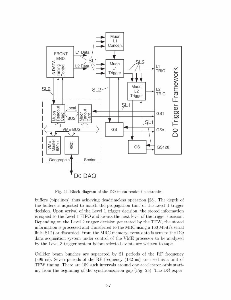
All muon detector subsystems have a common readout interface based on acommercial VME processor and two custom VME modules: the muon readoutcard (MRC) and the muon fanout card (MFC) described in Ref. [28]. Thereadout electronics is housed in eighteen 9U×280 mm VME crates. A blockdiagram of the muon electronics is shown in Fig. 24.
The DØ trigger framework (TFW) is the source of timing and control sig-nals for the entire experiment. The detector electronics is subdivided intoGeographic Sectors (GS) associated with the front-end detector electronics.Timing and trigger information is distributed to the GSs using 1 Gbit/s se-rial links (SL1). Each link is capable of transferring 96 bits of informationwithin 132 ns. A similar 1 Gbit/s link is used to transfer information from thefront-end electronics to the Level 1 trigger system.
All of the front-end crates are synchronized to the accelerator RF frequency(53.1047 MHz) allowing for accurate timing of the electronics to the colliderbeam. Detector signals are continuously digitized by charge-integrator/ADCor discriminator/time-digitizer signal processing chains and stored in circular
36
VME BUS
Local
BUSMuon
Fa
no
ut
Ca
rdR
eadout
Muon
Ca
rd
VM
EM
aste
r680xx
SB
C
Geographic Sector
FRONTEND
L3 D
AT
AT
imin
gC
ontr
ol
GS
GS
D0
Trig
ge
r F
ram
ew
ork
L1TRIG
L2TRIG
GS1
GSx
GS128
MuonL2
Trigger
MuonL1
Trigger
MuonL1
Concen.
L1 Data
L2 Data
SL2
SL1
SL2
SL1
SL1
SL2
D0 DAQ
Fig. 24. Block diagram of the DØ muon readout electronics.
buffers (pipelines) thus achieving deadtimeless operation [28]. The depth ofthe buffers is adjusted to match the propagation time of the Level 1 triggerdecision. Upon arrival of the Level 1 trigger decision, the stored informationis copied to the Level 1 FIFO and awaits the next level of the trigger decision.Depending on the Level 2 trigger decision generated by the TFW, the storedinformation is processed and transferred to the MRC using a 160 Mbit/s seriallink (SL2) or discarded. From the MRC memory, event data is sent to the DØdata acquisition system under control of the VME processor to be analyzedby the Level 3 trigger system before selected events are written to tape.
Collider beam bunches are separated by 21 periods of the RF frequency(396 ns). Seven periods of the RF frequency (132 ns) are used as a unit ofTFW timing. There are 159 such intervals around one accelerator orbit start-ing from the beginning of the synchronization gap (Fig. 25). The DØ exper-
37

Tevatron RFTev Sync
D0 TriggerFramework
Front-End Electronics
Tim
ing
FC
, G
AP
, S
GA
P, R
F
Contr
ol
L1acc,L
2acc,L
2re
j,B
x,IN
IT
BeamDelay
TimingLogic
PipelineDelay
L3 Data MRCD0Detector
7T
SGAP
GAP
GAP
L1
25T
T = 132 ns
Fig. 25. DØ muon detector timing. The circle represents the Tevatron ring filledwith particle bunches (solid line) with abort and synchronization gaps.
iment uses the Tevatron crossing number scheme to guarantee proper eventsynchronization. The seventh crossing after the beginning of synchronizationgap contains the first particle bunch. The specified delay between a beam col-lision and the arrival of the trigger signal from the Level 1 system at the TFWinput is twenty-five 132 ns intervals.
One of the important features of the muon electronics design is the achieve-ment of proper synchronization of all the elements of the system. To do this,the muon electronics has two variable digital delays implemented in the front-ends. The DØ TFW receives timing information from the accelerator andgenerates two sets of timing signals representing the timing structure of thecolliding beams: one for its own logic and the other for the DØ detector sub-systems (see Fig. 25). The latter has a timing offset to compensate for propa-gation delay in the cables. The offset is chosen so that timing signals arrive atthe front-end electronics at approximately the same time as the correspondingdetector signals arrive at the electronics inputs. Fine adjustments have to bedone using the so-called beam delay. The pipeline delay setting is affected bythe beam delay setting and vice versa. To overcome this difficulty, a proce-dure involving the internal test pulser is used to set the correct pipeline delayvalue. After the pipeline delay is selected, the beam delay value is adjustedusing beam data to compensate for cable delay differences. Any change in the
38
beam delay adjustment must be followed by an equal change of the pipelinedelay.
The muon front-end electronics includes PDT electronics, scintillation counterelectronics, and MDT electronics. The readout controllers for these subsystemshave similar designs and an Analog Devices ADSP-21csp01 50 MHz DSP. Thetime digitizers used in the PDT and scintillation counter electronics are basedon Toshiba TMC-TEG3 chips [29].
The PDTs have up to 96 signal wires per chamber. Attached to these chambersare four 24-channel front-end boards (FEB) and one control board (CB). TheFEBs digitize the time of arrival of the wire signal and the charge of the padelectrodes. The TMC chip is running at RF/2 frequency, providing 1.18 nsbin resolution. The digital delays and Level 1 FIFO buffers are also located onFEBs. Each FEB is connected to the CB via an 18 bit uni-directional data busand an 8-bit control bus. The CB has a readout controller, which fetches datasequentially from each FIFO. Upon receiving a Level 1 trigger, the controlleraccepts data and stores it in the DSP memory.
The front-end electronics of the scintillation counter system includes 48-channel9U VME scintillation counter front-end cards (SFE). These cards measure thearrival time of the scintillation counter signals. The TMC chip runs at 4/7 RFfrequency with a timing bin resolution of 1.03 ns. There are three charge inte-grators on each SFE with outputs digitized by ADCs. Each integrator inputcan be connected (multiplexed) to one of sixteen input channels to measurepulse height from the photomultiplier tube. The Level 1 FIFO buffers are readout by a DSP-based readout controller over a custom high speed data bus us-ing the VME J2 backplane. Each VME crate houses up to ten SFE cards, thereadout controller card, LED calibration electronics, and a Motorola 68EC040-based [30] VME processor to provide parameters downloading and testing.
The front-end electronics cards (ADBs) of the MDTs are located on the MDTchambers near the signal ends. Each ADB has 32 channels of amplifiers anddiscriminators. The digitization of the MDT wire signals is accomplished bya VME-based system. The digitization cards are 9U VME cards. Each cardcontains 192 channels. The MDT digitizing cards (MDCs) perform a low res-olution (18.8 ns/bin) measurement of the drift time. The MDC also has adigital pipeline and Level 1 FIFO buffers to store event data. A DSP-basedreadout controller reads out data over a custom VME J3 back plane. TheMDT crates can accommodate up to twelve MDCs, a readout controller, anda VME processor to perform tasks similar to those of the scintillation countersystem.
39
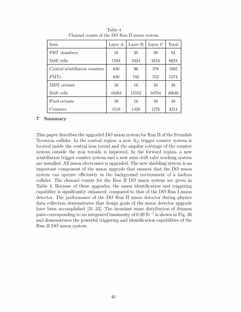
Table 4Channel counts of the DØ Run II muon system.
Item Layer A Layer B Layer C Total
PDT chambers 18 38 38 94
Drift cells 1584 2424 2616 6624
Central scintillation counters 630 96 276 1002
PMTs 630 192 552 1374
MDT octants 16 16 16 48
Drift cells 16384 15552 16704 48640
Pixel octants 16 16 16 48
Counters 1518 1420 1276 4214
7 Summary
This paper describes the upgraded DØ muon system for Run II of the FermilabTevatron collider. In the central region, a new Aϕ trigger counter system islocated inside the central iron toroid and the angular coverage of the countersystem outside the iron toroids is improved. In the forward region, a newscintillation trigger counter system and a new mini drift tube tracking systemare installed. All muon electronics is upgraded. The new shielding system is animportant component of the muon upgrade that ensures that the DØ muonsystem can operate efficiently in the background environment of a hadroncollider. The channel counts for the Run II DØ muon system are given inTable 4. Because of these upgrades, the muon identification and triggeringcapability is significantly enhanced, compared to that of the DØ Run I muondetector. The performance of the DØ Run II muon detector during physicsdata collection demonstrates that design goals of the muon detector upgradehave been accomplished [31–33]. The invariant mass distribution of dimuonpairs corresponding to an integrated luminosity of 0.20 fb−1 is shown in Fig. 26and demonstrates the powerful triggering and identification capabilities of theRun II DØ muon system.
40

]2) mass [GeV/c-µ +µInvariant (2 4 6 8 10 12
2E
vent
s / 2
0 M
eV/c
0
10000
20000
30000
40000
50000
60000ψJ/
’ψφω (1S, 2S, 3S) Υ
DØ
Fig. 26. Invariant mass of µ+µ− pairs detected by the DØ experiment in Run II.
References
[1] S. Abachi, et al., Nucl. Instr. and Meth. A 338 (1994) 185.
[2] C. Brown, et al., Nucl. Instr. and Meth. A 279 (1989) 331;Yu. Antipov, et al., Nucl. Instr. and Meth. A 297 (1990) 121.
[3] V. Abramov, et al., Nucl. Instr. and Meth. A 419 (1998) 660.
[4] R. Yamada, et al., IEEE Trans. Magnetics 28 (1) (1992) 520.
[5] Vector Fields Limited, 24 Bankside, Kidlington, Oxford, OX5 1JE, England.
[6] N. V. Mokhov, The MARS Code System User’s Guide, Fermilab-FN-0628, 1995;N. V. Mokhov, Status of MARS Code, Fermilab-Conf-03/053, 2003;http://www-ap.fnal.gov/MARS/.
[7] J. M. Butler, et al., Reduction of Tevatron and Main Ring Induced Backgroundsin the DØ Detector, Fermilab-FN-0629, 1995.
[8] H. T. Diehl, Aggressive Shielding Strategies for the Muon Upgrade, DØ Note2713, Fermilab, 1995;V. I. Sirotenko, D. S. Denisov, H. T. Diehl, DØ Shielding Optimization:Simulations and Measurements, DØ Note 3417, Fermilab, 1998.
[9] N. V. Mokhov, V. I. Sirotenko, Possible Minimal Solutions for DØ DetectorShielding Based on GCALOR and MARS13 Simulations, DØ Note 2601,Fermilab, 1995.
[10] G. Cosmo, S. Giani, N. J. Høimyr, et al., CERN-LHCC-95-70, CERN, Geneva,Switzerland, 1995.
[11] A. Bross, et al., The DØ Scintillating Fiber Tracker, Proceedings of the SCIFI97 Conference, p. 221, South Bend, Indiana, November, 1997.
41

[12] B. S. Acharya, et al., Nucl. Instr. and Meth. A 401 (1997) 45;V. Abramov, et al., IEEE Trans. Nucl. Sci. NS-46 (4) (1999) 865.
[13] EMI 9902K, Thorn EMI Gencom Inc., 23 Madison Rd., Fairfield, NJ 07006.
[14] Bicron Corporation, 12345 Kinsman Rd, Newbury, OH 44065-9677.
[15] V. Evdokimov, Light Collection from Scintillation Counters using WLS Fibersand Bars, Proceedings of the SCIFI 97 Conference, p. 300, South Bend, Indiana,November, 1997.
[16] MELZ, Electrozavodskaya str., 23, Moscow, Russia, 105023.
[17] Dupont De Nemours & Co., 705 Canter Rd., Rt. 141, Wilmington, DE 19810-1025.
[18] V. Bezzubov, et al., Fast Scintillation Counters with WLS Bars, Proceedings ofthe SCIFI 97 Conference, p. 210, South Bend, Indiana, November, 1997.
[19] S. Belikov, et al., Physical Characteristics of the SOFZ-105 PolymethylMethacrylate Secondary Emitter, Instruments and Experimental Technique, 36(1993) p. 390.
[20] S.-C. Ahn, et al., IEEE Nucl. Sci. Symposium, Vol. 2 (1991) 984.
[21] P. Hanlet, et al., Nucl. Instr. and Meth. A 521 (2004) 343.
[22] Glasteel Tennessee, Inc., 175 Commerce Rd, Collierville, TN 38017.
[23] T. Marshall, Nucl. Instr. and Meth. A 515 (2003) 50.
[24] W. Busza, Nucl. Instr. and Meth. A 265 (1988) 210.
[25] R. Veenhof, GARFIELD, A Drift Chamber Simulation Program, CERNProgram Library. http://garfield.web.cern.ch/garfield/
[26] G. D. Alexeev, et al., Nucl. Instr. and Meth. A 473 (2001) 269.
[27] T. Zhao, et al., IEEE Trans. Nucl. Sci. NS-49 (3) (2002) 1092.
[28] B. Baldin, et al., IEEE Trans. Nucl. Sci. NS-42 (4) (1995) 736.
[29] Y. Arai, F. Sudo and T. Emura, Developments of time memory cell VLSI’s,KEK Preprint 93-49, 1993.
[30] http://gocct.com/products/vme/motorola680x0.htm
[31] V. M. Abazov, et al., Phys. Rev. Lett. 93 (2004) 141801.
[32] V. M. Abazov, et al., Phys. Rev. Lett. 93 (2004) 162002.
[33] V. M. Abazov, et al., hep-ex/0409043; Fermilab-Pub-04/225-E (2004).
42