Embed Size (px)
Citation preview

Multiple Load-Source Integration in a Multilevel Modular Capacitor Clamped DC-DC Converter
Featuring Fault Tolerant Capability Faisa! H. Khan, Leon M. Tolbert
The University of Tennessee Electrical and Computer Engineering
Knoxville, TN 37996-2100 [email protected], [email protected]
Abstract-A multilevel modular capacitor clamped dc-dc converter (MMCCC) will be presented in this paper with some of its advantageous features. By virtue of the modular nature of the converter, it is possible to integrate multiple loads and sources to the converter at the same time. The modular construction of the MMCCC topology provides transformer like taps in the circuit, and depending on the conversion ratio of the converter, it becomes possible to connect several dc sources and loads at these taps. The modularity of the new converter is not limited to this transformer like operation, but also provides redundancy and fault bypass capability in the circuit. Using the modularity feature, some redundant modules can be operated in bypass state, and during any fault, these redundant modules can be used to replace a faulty module to maintain an uninterrupted operation. Thus, this MMCCC topology could be a solution to establish a power management system among multiple sources and loads having different operating voltages.
I. INTRODUCTION
In automotive applications, a high efficiency bi-directional dc-dc converter is a key element to provide the power for the electrical drive train. For this application, a justified choice might be a multilevel capacitor clamped dc-dc converter which can be operated at a very high efficiency. One of the major advantages of the capacitor clamped converter is that it can attain very high efficiency even at partial loads [1], where it is the opposite for classical dc-dc converters with an inductive energy transfer mechanism. There are several different types of multilevel dc-dc converters that have been previously developed [2-11]. The flying capacitor multilevel converter shown in [2][4] has some potential features to be used in automotive applications; however, it suffers from several limitations [1].
A modular circuit is advantageous over the non-modular structure for several reasons. If the circuit is modular, it is possible to distribute the total power handling capability among multiple modules used in the circuit; thereby low voltage/current stress is experienced by individual semiconductor devices in the circuit. In addition, a modular circuit could incorporate redundancy in the system that yields some fault tolerance properties of the circuit. Using the modularity, it is possible to localize any fault in the system, and the affected module can be bypassed and another good module activated, and thus a continuity of operation can be
1-4244-0714-1/07/$20.00 ©2007 IEEE. 361
maintained. Moreover, the faulty module can be physically removed from the system, and can be repaired or replaced by another module. This feature can facilitate easier maintenance and can obtain higher mean time between failures (MTBF).
This paper will present some new features of the multilevel modular capacitor-clamped dc-dc converter (MMCCC) that was presented in [1]. One of the key features of the MMCCC topology is that the circuit can be considered as a dc transformer having multiple taps where each module provides one intermediate voltage node. Using this feature of the circuit, it becomes possible to connect several dc voltage sources having different magnitudes simultaneously. Thus, the converter may eliminate the need of any power management unit that is a requirement for a system with more than two voltage sources and loads. Moreover, it will also be shown how multiple loads can be connected across the voltage nodes so that several voltage outputs can be obtained from the circuit simultaneously. In section II-IV, the new topology and the multiple load/source integration technique will be presented along with simulation and experimental results. Section III will explain the de transformer action of the converter, and section V will present the redundancy and fault bypass feature of the converter.
II. MMCCC TOPOLOGY
The proposed 5-level MMCCC shown in Fig. 1 has an inherent modular structure and can be designed to achieve any conversion ratio. Each modular block has one capacitor and three transistors leading to three terminal points. A modular block is shown in Fig. 2. The terminal V in is connected to either the high voltage battery or to the output of the previous stage. One of the output terminals V next is connected to the input of the next stage. The other output terminal VLV is connected to the low voltage side + battery terminal or load.
In a flying capacitor multilevel dc-dc converter (FCMDC) with conversion ratio of 5, the total operation takes 5 subintervals [1], and this is shown in Table 1. Only one chargedischarge operation is performed in one sub interval. Thus, the component utilization becomes limited in this circuit. For an N-Ievel FCMDC circuit, any capacitor except C1 is utilized during only two sub-intervals for a complete cycle (one sub interval for charging, one for discharging) and for the

Fig. 1. The proposed 5-level MMCCC with four modular blocks.
remaining three sub-intervals in one period, the component is not used. The MMCCC topology can increase the component utilization by performing multiple operations at the same time, which is shown in Table 1.
The switching sequence in the MMCCC circuit works in a simpler way than the FCMDC converter. As there are only two sub-intervals, two switching states are present in the circuit. Switches SRI to SR7 in Fig. 1 are operated at the same time to achieve state 1. In the same way switches SBI to SB6 are operated simultaneously to make state 2, and this gate signal sequence is shown in Fig. 3. The detail operation of the MMCCC topology can be found in [1].
III. MULTIPLE LoAD-SOURCE INTEGRATION
A. Source Integration
The modular MMCCC topology can be used to integrate multiple voltage sources simultaneously to build a power management system among various voltage sources. The 5-level MMCCC circuit shown in Fig. 1 has 4 modules, and every module's input port creates a voltage node in the circuit. Fig. 4 shows a 6-level MMCCC converter, and analytically computed voltage levels generated at nodes 1 to 6 are shown. This figure shows that each node produces a time varying dc voltage with an ac voltage superimposed it. The amplitude of the ac voltage swing is equal to 1VLV or VI. The voltages at different nodes are summarized in Table 2.
Fig. 2. The unique modular block.
TABLE 1. SWITCHING SCHEMES OF FCMDC AND THE MMCCC CIRCUIT. t = CHARGING,..l.= DISCHARGING
FCMDC MMCCC Sub Operations Sub Operations
interval interval No. No. I VIN->Cst +clt I VIN->Cst +clt
2 Cs..l. -> C4 t + Cl t c 4..l. -> C3 t + Cl t
3 c 4..l. -> c 3t + Cit Cz..l. -> Cit
4 c 3..l. -> Czt + Cit 2 CS..l.->c4t +clt
5 Cz..l. -> Cit c 3..l. -> Cz t + Cl t
Using this time varying nature of these node voltages, some additional voltage sources can be connected at these nodes. Inherently, the MMCCC circuit is a bi-directional converter and it can be used to manage the power flow between V HV and VLV (Fig. 1) by controlling the conversion ratio (CR) of the circuit, and the number of active levels present in the circuit governs the CR. The added functionality of the multiple source integration can facilitate a system to integrate up to 7 voltage sources for a 6-level converter; which means 5 additional voltage sources at nodes 2 to 6 can be connected. This feature may be used to integrate various kinds of energy sources such as solar cell, fuel cell, battery etc. having different voltages in the same system.
Table 2 shows the simulated values of the time varying voltages at different nodes of the 6-level MMCCC circuit for the two states present in the circuit. At state 1, the voltage at
SR
o TI2 T
SB
o TI2 T
Fig. 3. The gating signal of the switches in the MMCCC circuit, i.e. there are only two switching states present in the circuit.
362

1-- 1- 1-- 1- 1-- 1--
Fig. 4. The simulation results of the intermediate node voltages in a 6-level MMCCC circuit. The voltage magnitude at any node printed in black is the value during state 1, the value printed in gray is the voltage magnitude during state 2.
node 5 is 4VLV, and during state 2, the voltage is 5VLV• Thus, if an external voltage source of amplitude 4VLV is connected to node 2, it will contribute power along with V HV to the low voltage side of the converter during state 1. During state 2, the voltage at node 5 becomes 5VLV, which is higher than the external source voltage; thus the converter will not draw any power from the external source connected at this node. In the same way, four other voltage sources can be connected at nodes 2, 3, 4, and 6.
While connecting multiple sources in the system, one issue needs to be considered to keep the output voltage ripple the same as in the case when only V HV is connected to the system.
TABLE 2. THE TIME VARYING NODE VOLTAGES OF A 6-LEVEL
MMCCC CIRCUIT
State Active
V6 Vs V4 V3 V2 Switches
1 SR1-SR7 6VLV 4VLV 4VLV 2VLV 2VLV
2 SB1-SB6 SVLV SVLV 3VLV 3VLV IVLv
Load 64
v
Load 53
To achieve this, the current shared by the external sources must be in phase with the current provided by VHV• Table 1 shows that the converter takes power from V HV during state 1 only. Thus, the additional voltage sources must be connected in the system in such a way that they provide power during state 1 only. As mentioned earlier, the magnitude of an external voltage source needs to be close to the lower value among the two voltage levels present at any node, and this is required to bring a balance between the voltage at the node and the external source. Thus, if an external voltage source needs to be connected at node 6, its magnitude needs to be close to 5VLV• At node 6, the voltage varies between 6VLV and 5VLV,
and during state 1, the voltage is 6VLV• Thus, it is not possible to connect a voltage source at node 6 while keeping the output voltage ripple unaffected. For the same reason, node 4 and node 2 will not be suitable for integrating a voltage source in this 6-level converter. Fig. 5 shows the integration of two external sources connected at nodes 3 and 5, because they share the load current during state 1 only. However, it is always possible to connect voltage sources at any node, but a compromise must be made with the output voltage ripple.
B. Load Integration
The other advantage of this integration feature is the ability
Load 42
Fig. S. The schematic diagram of the integration of multiple sources and loads in a 6-level MMCCC circuit.
363
to connect multiple loads at the same time. Fig. 4 shows the no-load voltages at different nodes of the MMCCC circuit. Nodes 2-6 generate time varying dc voltages; however, a dc load cannot be connected between any of these nodes and ground. This figure shows that the time varying voltage at node 2, 4, and 6 have the same phase. This is true for node 3 and 5 also. Thus, it is possible to connect a load in various ways between these in-phase nodes. Fig. 5 shows how loads can be connected between nodes (6, 4), (5, 3), and (4, 2) to obtain a constant dc voltage across the loads. The voltage difference between two adjacent in-phase nodes is 2VLV. In the same way, the voltage difference between node 6 and 2 is 4VLV. Thus, it is possible to connect multiple loads of 1 VLV, 2VLV, and 4VLV simultaneously in a 6-level MMCCC circuit.
IV. EXPERIMENTAL RESULTS
To verify the concept of integrating multiple loads and sources in the circuit, an experimental setup was made, and the schematic in Fig. 5 was followed. A 500 W 6-level MMCCC prototype shown in Fig. 6 was used. Three bench top power supplies were used as VHV, YES, and VE3, and a diode was used in series with each voltage so~ to protect the power supplies fro~verse power flow. A 3 ~ .&ad was used as RLV, and two 24 ~ Aoads w~ used as Load42 and Loads3. In addition to them, one 48 ~ .load was used as a load connected between node 6 and 2. The main input voltage VHV was kept at 75 V.
Fig. 7(a) shows the no-load voltages at HV (the cathode terminal of the diode connected to V HV), V 6 and V S nodes. Fig. 7(b) shows the voltages recorded at V4, V3, V2, and VI nodes. These voltages have the same variations in phase and magnitude found in the simulation (shown in Fig. 4) and analytical computation. The voltages at nodes 2-6 have a swing of 1 VLV. Thus, the voltage at node 2 varies between 12.3 V and 25 V. There was a small variation found at HV node though it was supposed to be a constant value of 75 V obtained from VHV. This voltage was measured at the converter board and not across the power supply terminals. Due to the voltage drop across the current sampling resistor and wire stray inductance, a small ripple was observed at this voltage input port of the converter.
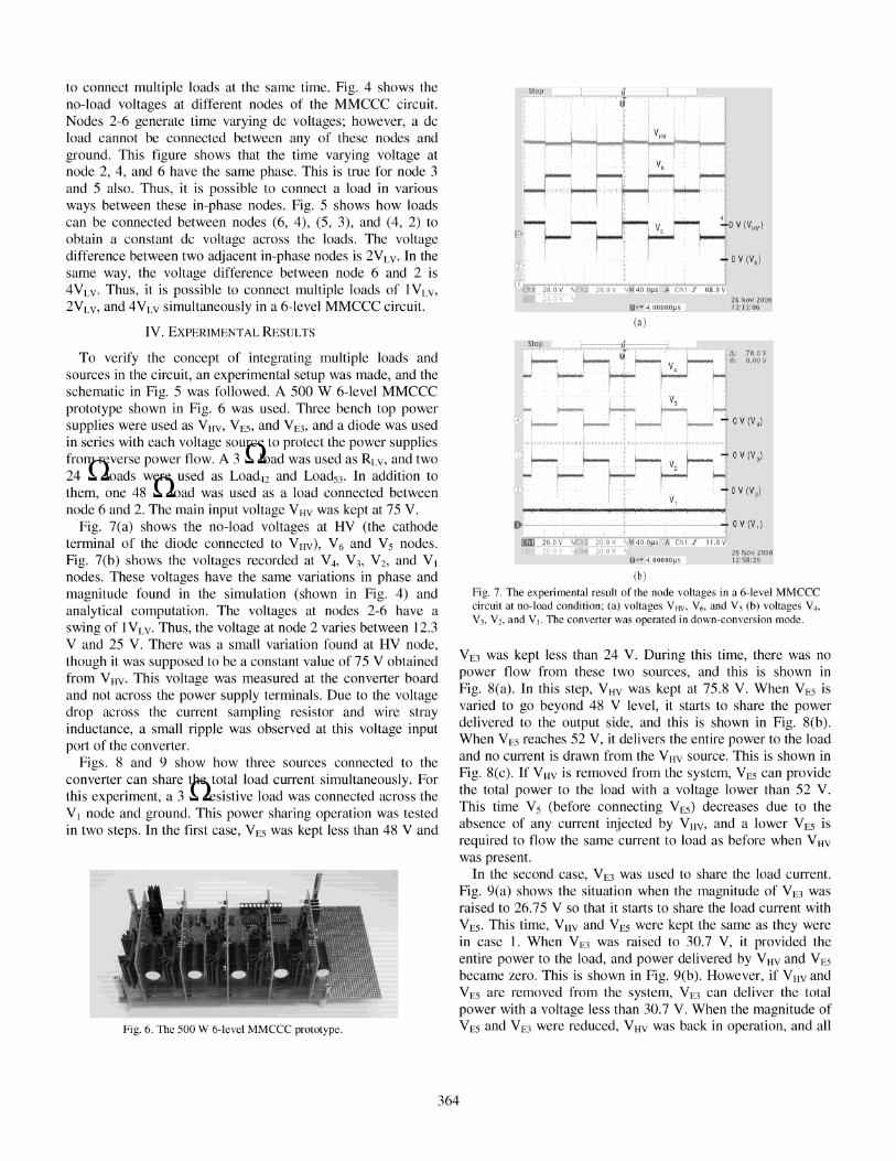
Figs. 8 and 9 show how three sources connected to the converter can share ~ total load current simultaneously. For this experiment, a 3 !:.lesistive load was connected across the V I node and ground. This power sharing operation was tested in two steps. In the first case, VES was kept less than 48 V and
Fig. 6. The 500 w 6-level MMCCC prototype.
(a)
(b)
Fig. 7. The experimental result of the node voltages in a 6-level MMCCC circuit at no-load condition; Ca) voltages VIN• V6• and Vs Cb) voltages V4•
V3• V2• and VI. The converter was operated in down-conversion mode.
VE3 was kept less than 24 V. During this time, there was no power flow from these two sources, and this is shown in Fig. 8(a). In this step, VHV was kept at 75.8 V. When VES is varied to go beyond 48 V level, it starts to share the power delivered to the output side, and this is shown in Fig. 8(b). When VES reaches 52 V, it delivers the entire power to the load and no current is drawn from the V HV source. This is shown in Fig. 8(c). If VHV is removed from the system, VES can provide the total power to the load with a voltage lower than 52 V. This time Vs (before connecting YES) decreases due to the absence of any current injected by VHV, and a lower VES is required to flow the same current to load as before when V HV
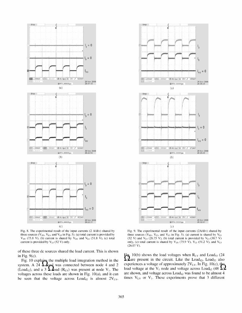
was present. In the second case, V E3 was used to share the load current.
Fig. 9(a) shows the situation when the magnitude of VE3 was raised to 26.75 V so that it starts to share the load current with YES. This time, VHV and VES were kept the same as they were in case 1. When VE3 was raised to 30.7 V, it provided the entire power to the load, and power delivered by VHvand VES became zero. This is shown in Fig. 9(b). However, if VHV and V ES are removed from the system, V E3 can deliver the total power with a voltage less than 30.7 V. When the magnitude of V ES and V E3 were reduced, V HV was back in operation, and all
364
(a)
(b)
(e)
Fig. 8. The experimental result of the input currents (2 Aldiv) shared by three sources (VIN, YES, and VE3 in Fig. 5). (a) total current is provided by VIN (75.8 V), (b) current is shared by VIN and VES (51.8 V), (c) total current is provided by VES (52 V) only.
of these three dc sources shared the load current. This is shown in Fig. 9(c).
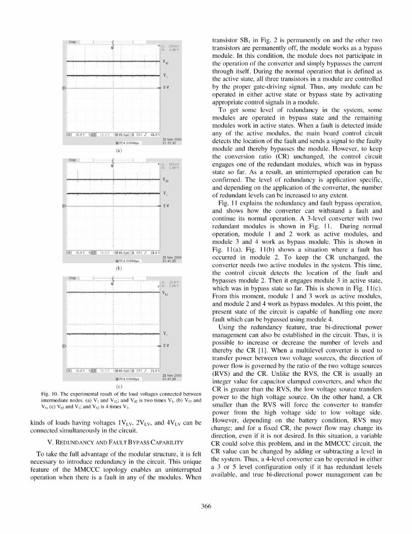
Fig. 10 eXPl~' the multiple load integration method in the system. A 24 was connected between node 4 and 2 (Loadd, and a 3 ad (RLV) was present at node VI. The voltages across these loads are shown in Fig. lO(a), and it can be seen that the voltage across Load42 is almost 2VLV•
365
(a)
(b)
(e)
Fig. 9. The experimental result of the input currents (2A1div) shared by three sources (VIN, VES, and VE3 in Fig. 5). (a) current is shared by VES (52 V) and VE3 (26.75 V), (b) total current is provided by VE3 (30.7 V) only, (c) total current is shared by VIN (75.9 V), VES (51.2 V), and VE3 (26.07 V).
~ 1 O(b) shows the load voltages when RL v and Loads3 (24 ~ ~ are present in the circuit. Like the Loa~2' Loads3 also experiences a voltage of approximately 2VLV• In Fig. lO(c), t~ load voltage at the VI node and voltage across Loa~2 (48 ~~ are shown, and voltage across Loadu2 was found to be almost 4 times V LV or V I. These experiments prove that 3 different
(a)
(b)
(c)
Fig. 10. The experimental result of the load voltages connected between intermediate nodes. (a) VI and V42 ; and V42 is two times VI. (b) V53 and VI. (c) V62 and VI; and V62 is 4 times VI.
kinds of loads having voltages IVLv, 2VLV, and 4VLV can be connected simultaneously in the circuit.
V. REDUNDANCY AND FAULT BYPASS CAPABILITY
To take the full advantage of the modular structure, it is felt necessary to introduce redundancy in the circuit. This unique feature of the MMCCC topology enables an uninterrupted operation when there is a fault in any of the modules. When
transistor SB1 in Fig. 2 is permanently on and the other two transistors are permanently off, the module works as a bypass module. In this condition, the module does not participate in the operation of the converter and simply bypasses the current through itself. During the normal operation that is defined as the active state, all three transistors in a module are controlled by the proper gate-driving signal. Thus, any module can be operated in either active state or bypass state by activating appropriate control signals in a module.
To get some level of redundancy in the system, some modules are operated in bypass state and the remaining modules work in active states. When a fault is detected inside any of the active modules, the main board control circuit detects the location of the fault and sends a signal to the faulty module and thereby bypasses the module. However, to keep the conversion ratio (CR) unchanged, the control circuit engages one of the redundant modules, which was in bypass state so far. As a result, an uninterrupted operation can be confirmed. The level of redundancy is application specific, and depending on the application of the converter, the number of redundant levels can be increased to any extent.
Fig. 11 explains the redundancy and fault bypass operation, and shows how the converter can withstand a fault and continue its normal operation. A 3-level converter with two redundant modules is shown in Fig. 11. During normal operation, module 1 and 2 work as active modules, and module 3 and 4 work as bypass module. This is shown in Fig. 11 (a). Fig. l1(b) shows a situation where a fault has occurred in module 2. To keep the CR unchanged, the converter needs two active modules in the system. This time, the control circuit detects the location of the fault and bypasses module 2. Then it engages module 3 in active state, which was in bypass state so far. This is shown in Fig. l1(c). From this moment, module 1 and 3 work as active modules, and module 2 and 4 work as bypass modules. At this point, the present state of the circuit is capable of handling one more fault which can be bypassed using module 4.
Using the redundancy feature, true bi-directional power management can also be established in the circuit. Thus, it is possible to increase or decrease the number of levels and thereby the CR [1]. When a multilevel converter is used to transfer power between two voltage sources, the direction of power flow is governed by the ratio of the two voltage sources (RVS) and the CR. Unlike the RVS, the CR is usually an integer value for capacitor clamped converters, and when the CR is greater than the RVS, the low voltage source transfers power to the high voltage source. On the other hand, a CR smaller than the RVS will force the converter to transfer power from the high voltage side to low voltage side. However, depending on the battery condition, RVS may change; and for a fixed CR, the power flow may change its direction, even if it is not desired. In this situation, a variable CR could solve this problem, and in the MMCCC circuit, the CR value can be changed by adding or subtracting a level in the system. Thus, a 4-level converter can be operated in either a 3 or 5 level configuration only if it has redundant levels available, and true bi-directional power management can be
366

iHV iHV VHV VHV
T T (a) (b)
iHV Good module in I Faulty active state module
T D Good module in ...... Indication of bypass state bypass operation
(c)
Fig. 11. The redundancy and fault withstand capability of the converter, (a) a three level converter running at normal operating mode with two redundant modules (3 and 4), (b) a fault occurred in module 2, (c) module 2 went into bypass mode and replaced by module 3.
established. For a finer control on the CR, the duty ratio of the gate drive signal may be changed, and it becomes possible to get a more precise control of the current. This can be considered as a future work at this point.
VI. CONCLUSIONS
A new topology of modular multilevel dc-dc converter has been proposed, and the multiple load/source integration technique has been presented and verified through experiments. The test results show that several voltage sources can be connected to the different nodes of the circuit, and load power requirement can be mitigated by those voltage sources in a combined fashion. Thus, it becomes possible to get variable conversion ratio from the circuit, and a complete power management protocol can be established among various voltage sources. Moreover, the circuit can generate different load voltages simultaneously, and this feature makes it possible to obtain various output voltages from a wide input voltage range. Thus, this feature simply helps to consider the MMCCC converter as a dc transformer having multiple taps to connect multiple loads and dc sources at the same time.
In addition to this feature, the modular nature of the MMCCC topology can be successfully used to get redundancy and fault bypassing capability in the system. This feature can increase the reliability of the system and decreases the down time of the converter. Above all, the circuit is capable of bidirectional power handling, and all these features make the MMCCC topology a suitable candidate in various applications.
ACKNOWLEDGEMENT
We would like to thank Oak Ridge National Laboratory for supporting this work through UT-Battelle contract no. 4000007596.
REFERENCES [1] Faisal H. Khan, Leon M. Tolbert, "A Multilevel Modular Capacitor
Clamped DC-DC converter," IEEE Industry Applications Annual Meeting (lAS), Oct. 2006.
[2] Z. Pan, F. Zhang, F. Z. Peng, "Power Losses and Efficiency Analysis of Multilevel DC-DC Converters," IEEE Applied Power Electronics Conference (APEC), pp. 1393-1398, March 2005.
367
[3] F. Zhang, F. Z. Peng, Z. Qian, "Study of Multilevel Converters in DCDC Application," IEEE Power Electronics Specialists Conference (PESC), pp. 1702-1706, June 2004.
[4] F. Z. Peng, F. Zhang, Z. Qian, "A Novel Compact DC-DC Converter for 42V Systems," IEEE Power Electronics Specialists Conference (PESC), pp. 33-38, June 2003.
[5] K. D. T. Ngo, R. Webster, "Steady-State Analysis and Design of a Switched-Capacitor DC-DC Converter," IEEE Transactions on Aero. and Elec. Systems, vol. 30, no. 1, pp. 92-101, Jan. 1994.
[6] W. Harris, K. Ngo, "Power Switched-Capacitor DC-DC Converter, Analysis and Design," IEEE Transactions on Aero. and Elec. Systems, vol. 33, no. 2, pp. 386-395, April 1997.
[7] S. V. Cheong, H. Chung, A. Ioinovici, "Inductorless DC-to-DC Converter with High Power Density," IEEE Transactions on Industrial Electronics, vol. 41, no. 2, pp. 208-215, April 1994.
[8] O. Mak, Y. Wong, A. Ioinovici, "Step-up DC Power Supply Based on a Switched-Capacitor Circuit," IEEE Transactions on Industrial Electronics, vol. 42, no. 1, pp. 90-97, Feb. 1994.
[9] c. K. Tse, S.C. Wong, M. H. L. Chow, "On Lossless SwitchedCapacitor Power Converters," IEEE Transactions on Power Electronics, vol. 10, no. 3, pp. 286-291, May 1995.
10] E. Bayer, "Optimized Control of the 'Flying' -Capacitor Operating Voltage in 'Gear-Box' -Charge Pumps, - The Key Factor for a Smooth Operation," IEEE Power Electronics Specialists Conference (PESC), pp. 610-615, June 2003.
[11] R. D. Middlebrook, "Transformerless DC-to-DC Converters with Large Conversion Ratios," IEEE Transactions on Power Electronics, vol. 3, no. 4, pp. 484-488, October 1988.