Embed Size (px)
Citation preview
Department of EECS University of California, Berkeley
EECS 105 Spring 2017, Module 3
Prof. Ali M. Niknejad Prof. Rikky Muller
MOS Capacitors
EE 105 Spring 2017 Prof. A. M. Niknejad Prof. Rikky Muller
2
Announcements l Welcome to the second half of EE105! l Professor Muller will be lecturing
l Midterm 1 handed back today l Mean = l Median = l Standard Dev =
l Midterm 2 on Thursday, March 23 in lecture
l Attend discussion sessions! They are helpful for homework, exam reviews and topics not covered in lecture.
University of California, Berkeley

EE 105 Spring 2017 Prof. A. M. Niknejad Prof. Rikky Muller
3
MOS Capacitor
l MOS = Metal Oxide Semiconductor l Sandwich of conductors separated by an insulator l “Metal” is more commonly a heavily doped polysilicon
(poly-Si) layer n+ or p+ layer – Was metal (e.g. Al) until ~1970 but changed to poly-Si due to high
temperature processing. After 2008, metal gates have been reintroduced! Learn more about MOS process technology in EE130 & EE143
l NMOS à p-type substrate, PMOS à n-type substrate University of California, Berkeley
Oxide (SiO2)
Body (p-type substrate)
Gate (n+ poly)
011.7sε ε=
03.9oxε ε=
Very Thin!
~1nmoxtx
0

EE 105 Spring 2017 Prof. A. M. Niknejad Prof. Rikky Muller
4
Metal-Oxide-Semi Junction
l Under thermal equilibrium, the n-type poly gate is at a higher potential than the p-type substrate
l No current can flow because of the insulator but this potential difference is accompanied with an electric field
l Fields terminate on charge!
University of California, Berkeley
φ p = −kTqlnNani
φpoly ,n+
=kTqlnNd ,polyni
⎛
⎝⎜⎜
⎞
⎠⎟⎟ ≈ 550mV
Body (p-type substrate)
Gate (n+ poly)

EE 105 Spring 2017 Prof. A. M. Niknejad Prof. Rikky Muller
5
Fields and Charge at Equilibrium
l At equilibrium there is an electric field from the gate to the body
l Need a positive charge on the gate, negative charge in substrate
l Since body is p-type, negative charges in the body come from a depletion region
University of California, Berkeley
Body (p-type substrate)
++++++++++++++++++ − − − − − − − − − − − − − − − − − − − − − − − − − − 0dX
+
− oxV +
− BV oxE

EE 105 Spring 2017 Prof. A. M. Niknejad Prof. Rikky Muller
6
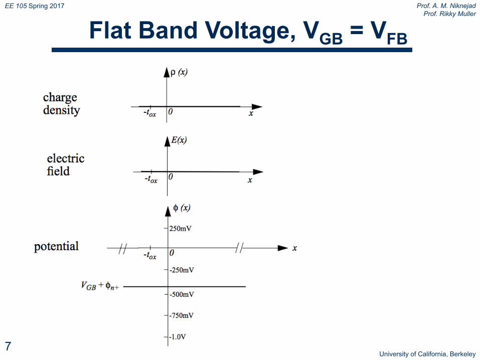
Flat Band Voltage, VGB = VFB
l If we apply a bias, we can compensate for this built-in potential
l In this case the charge on the gate goes to zero and the depletion region disappears
l In solid-state physics lingo, the energy bands are “flat” under this condition
University of California, Berkeley
( )FB pnV φ φ+= − −
( ) 0G GB FBQ V V= =
Body (p-type substrate)
+ − 0FBV <
EE 105 Spring 2017 Prof. A. M. Niknejad Prof. Rikky Muller
7
Flat Band Voltage, VGB = VFB
University of California, Berkeley
EE 105 Spring 2017 Prof. A. M. Niknejad Prof. Rikky Muller
8
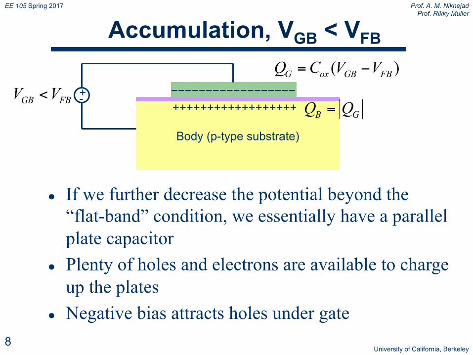
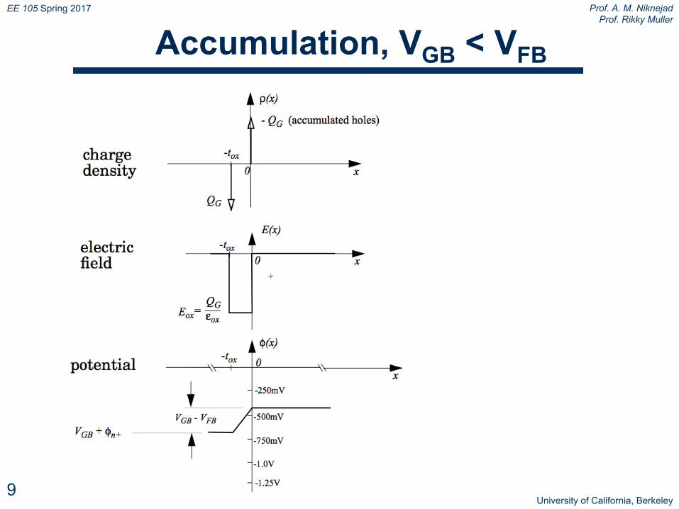
Accumulation, VGB < VFB
l If we further decrease the potential beyond the “flat-band” condition, we essentially have a parallel plate capacitor
l Plenty of holes and electrons are available to charge up the plates
l Negative bias attracts holes under gate
University of California, Berkeley
( )G ox GB FBQ C V V= −
Body (p-type substrate)
+ - GB FBV V<++++++++++++++++++ −−−−−−−−−−−−−−−−−−
B GQ Q=
EE 105 Spring 2017 Prof. A. M. Niknejad Prof. Rikky Muller
9
Accumulation, VGB < VFB
University of California, Berkeley

EE 105 Spring 2017 Prof. A. M. Niknejad Prof. Rikky Muller
10
Depletion, VGB > VFB
l Similar to equilibrium, the potential in the gate is higher than the body
l Body charge is made up of the depletion region ions
l Potential drop across the body and depletion region
University of California, Berkeley
Body (p-type substrate)
+ − GB FBV V> + + + + + + + + + +
( )B a d GBQ qN X V= −− − − − − − − − − − − − − − − − −
( )G GB BQ V Q= −

EE 105 Spring 2017 Prof. A. M. Niknejad Prof. Rikky Muller
11
Depletion, VGB > VFB
University of California, Berkeley

EE 105 Spring 2017 Prof. A. M. Niknejad Prof. Rikky Muller
12
Inversion, VGB > VT
l As we further increase the gate voltage, eventually the surface potential increases to a point where the electron density at the surface equals the background ion density
l At this point, the depletion region stops growing and the extra charge is provided by the inversion charge at surface
l “Inversion” meaning that the surface is effectively n-type University of California, Berkeley
Body (p-type substrate)
+ + + + + + + + + + + − GB TV V=− − − − − − − − − − − − − − − − −
sqkT
s i an n e Nφ
= = s pφ φ= −
sφ

EE 105 Spring 2017 Prof. A. M. Niknejad Prof. Rikky Muller
13
Inversion, VGB > VT
University of California, Berkeley

EE 105 Spring 2017 Prof. A. M. Niknejad Prof. Rikky Muller
14
Threshold Voltage
l The threshold voltage is defined as the gate-body voltage that causes the surface to change from p-type to n-type
l For this condition, the surface potential has to equal the negative of the p-type potential
l We can derive that this voltage is equal to:
University of California, Berkeley
12 2 ( 2 )Tn FB p s a pox
V V q NC
φ ε φ= − + −

EE 105 Spring 2017 Prof. A. M. Niknejad Prof. Rikky Muller
15 University of California, Berkeley
Recap Accumulation: VGB < VFB
l Essentially a parallel plate capacitor l Capacitance is determined by oxide thickness
( )G ox GB FBQ C V V= −
Body (p-type substrate)
− + GB FBV V<++++++++++++++++++ −−−−−−−−−−−−−−−−−−
B GQ Q=
EE 105 Spring 2017 Prof. A. M. Niknejad Prof. Rikky Muller
16 University of California, Berkeley
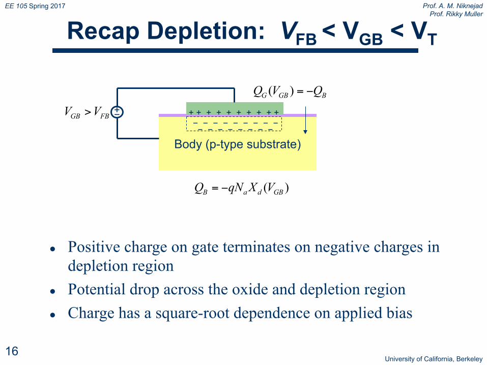
Recap Depletion: VFB < VGB < VT
l Positive charge on gate terminates on negative charges in depletion region
l Potential drop across the oxide and depletion region l Charge has a square-root dependence on applied bias
Body (p-type substrate)
+ − GB FBV V> + + + + + + + + + +
( )B a d GBQ qN X V= −
− − − − − − − − − − − − − − − − −
( )G GB BQ V Q= −

EE 105 Spring 2017 Prof. A. M. Niknejad Prof. Rikky Muller
17 University of California, Berkeley
Recap Inversion: VGB > VT
l The surface potential increases to a point where the electron density at the surface equals the background ion density
l At this point, the depletion region stops growing and the extra charge is provided by the inversion charge (electrons) at the surface
sqkT
s i an n e Nφ
= =
Body (p-type substrate)
+ + + + + + + + + + + − GB TV V=
− − − − − − − − − − − − − − − − −
sφ

EE 105 Spring 2017 Prof. A. M. Niknejad Prof. Rikky Muller
18
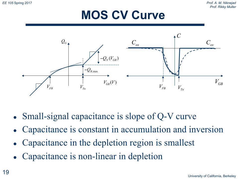
Q-V Curve for MOS Capacitor
l In accumulation, the charge is simply proportional to the applies gate-body bias
l In inversion, the same is true l In depletion, the charge grows slower since the
voltage is applied over a depletion region University of California, Berkeley
GQ
( )GBV VTnVFBV
depletion
,maxBQ−
( )N GBQ V−
EE 105 Spring 2017 Prof. A. M. Niknejad Prof. Rikky Muller
19
MOS CV Curve
l Small-signal capacitance is slope of Q-V curve l Capacitance is constant in accumulation and inversion l Capacitance in the depletion region is smallest l Capacitance is non-linear in depletion
University of California, Berkeley
GQ
( )GBV VTnVFBV
,maxBQ−
( )N GBQ V−
C
GBV
oxC oxC
TnVFBV
EE 105 Spring 2017 Prof. A. M. Niknejad Prof. Rikky Muller
20
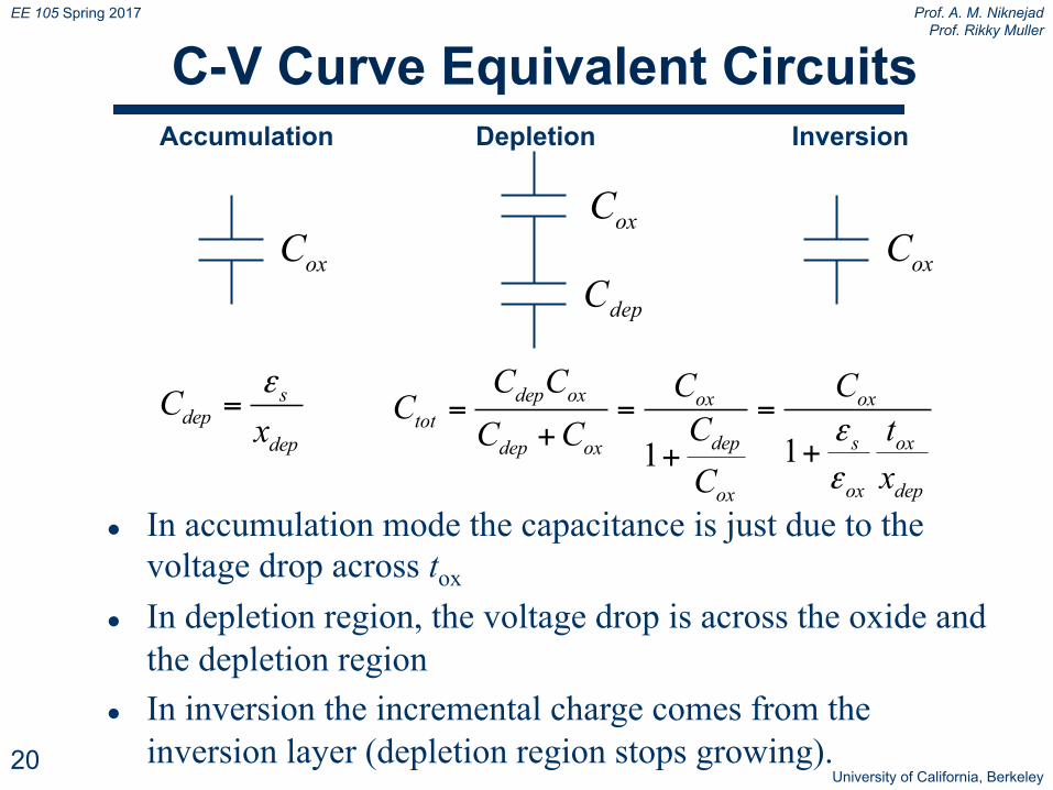
C-V Curve Equivalent Circuits
l In accumulation mode the capacitance is just due to the voltage drop across tox
l In depletion region, the voltage drop is across the oxide and the depletion region
l In inversion the incremental charge comes from the inversion layer (depletion region stops growing).
University of California, Berkeley
oxC oxCoxC
depC
sdep
dep
Cxε
=11
dep ox ox oxtot
dep s oxdep ox
ox depox
C C C CC C tC CxC
εε
= = =+ ++
Accumulation Depletion Inversion

EE 105 Spring 2017 Prof. A. M. Niknejad Prof. Rikky Muller
21
Numerical Example
l MOS Capacitor with p-type substrate:
l Calculate flat-band:
l Calculate threshold voltage:
University of California, Berkeley
20nmoxt = 16 35 10 cmaN−= ×
( ) (550 ( 402)) 0.95VFB pnV φ φ+= − − = − − − = −
12 2 ( 2 )Tn FB p s a pox
V V q NC
φ ε φ= − + −
13
-6
3.45 10 F/cm2 10 cm
oxox
ox
Ctε −×
= =×
19 12 162 1.6 10 1.04 10 5 10 2 0.4.95 2( 0.4) 0.52VTnox
VC
− −× × × × × × × ×= − − − + =

EE 105 Spring 2017 Prof. A. M. Niknejad Prof. Rikky Muller
22
Num Example: Electric Field in Oxide
l Apply a gate-to-body voltage:
l Device is in accumulation l The entire voltage drop is across the oxide:
l The charge in the substrate (body) consist of holes:
University of California, Berkeley
2.5GB FBV V= − <
56
2.5 0.55 ( 0.4) V8 102 10 cm
GB pox nox
ox ox
VVEt t
φ φ+
−
+ − − + − −= = = = − ×
×
7 2( ) 2.67 10 C/cmB ox GB FBQ C V V −= − − = ×