Embed Size (px)
Citation preview

Department of EECS University of California, Berkeley
Prof. Ali M. Niknejad
Differential Amplifiers

EE 105 Fall 2016 Prof. A. M. Niknejad
2
Why Differential?
z Differential circuits are much less sensitive to noises and interferences
z Differential configuration enables us to bias amplifiers and connect multiple stages without using coupling or bypass capacitors
z Differential amplifiers are widely used in IC’s– Excellent matching of transistors, which is critical for
differential circuits– Differential circuits require more transistors Æ not an
issue for IC

EE 105 Fall 2016 Prof. A. M. Niknejad
3
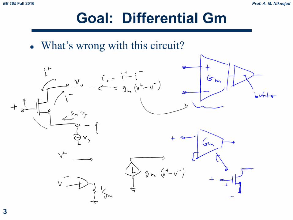
Goal: Differential Gm
z What’s wrong with this circuit?

EE 105 Fall 2016 Prof. A. M. Niknejad
4
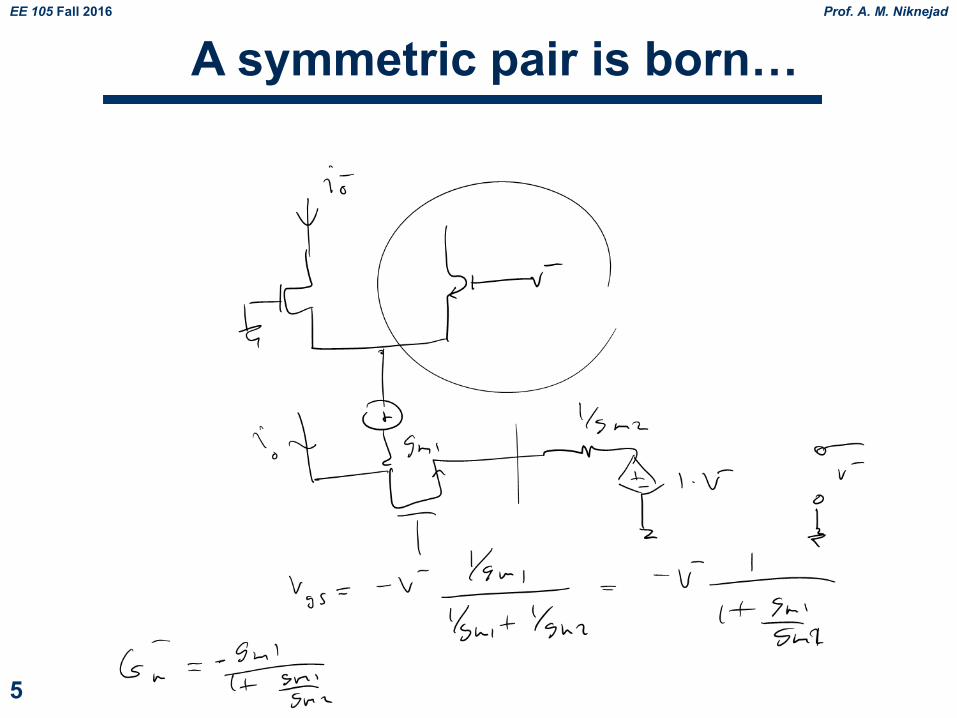
Add a buffer to source side…
EE 105 Fall 2016 Prof. A. M. Niknejad
5
A symmetric pair is born…

EE 105 Fall 2016 Prof. A. M. Niknejad
6
MOS Differential-Pair Basic Configuration

EE 105 Fall 2016 Prof. A. M. Niknejad
7
Common Mode InputsDifferential Pair
Rejects Common-Mode Inputs

EE 105 Fall 2016 Prof. A. M. Niknejad
11
Small Signal Operation

EE 105 Fall 2016 Prof. A. M. Niknejad
12
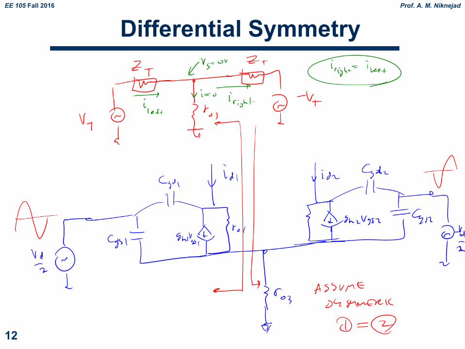
Differential Symmetry

EE 105 Fall 2016 Prof. A. M. Niknejad
13
Differential Half Circuit
Q1 biased at I2
Ad =vod2vid2
= vodvid
= gm RD || ro( )

EE 105 Fall 2016 Prof. A. M. Niknejad
16
CM Symmetry

EE 105 Fall 2016 Prof. A. M. Niknejad
17
CM AC Equivalent Circuit
Non-ideal current source consists of an ideal current source shunted by a large resistance, RSS
EE 105 Fall 2016 Prof. A. M. Niknejad
18
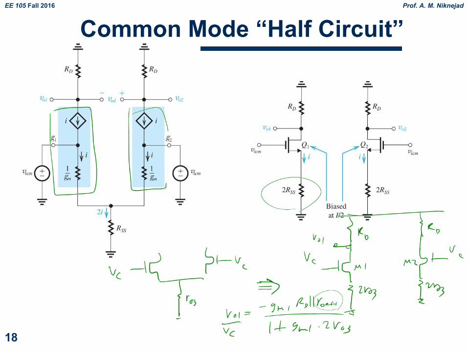
Common Mode “Half Circuit”

EE 105 Fall 2016 Prof. A. M. Niknejad
19
Ideal CM Output Voltage
Common-Source with degeneration

EE 105 Fall 2016 Prof. A. M. Niknejad
20
Common Mode Gain with Mismatched RDHowever, any mismatch in the half circuitswill produce finite output voltage, e.g., RD2 = RD +DRD
vod = vo2 - vo1 =- DRD2RSS
vicm
Common mode gain:
Acm =vodvicm
= - DRD2RSS
= - RD2RSS
æ
èç
ö
ø÷DRDRD
æ
èç
ö
ø÷
Common Mode Rejection Ratio (CMRR):
CMRR ºAdAcm
, in dB: CMRR(dB) º 20 logAdAcm
CMRR should be as large as possible. For the above case,
CMRR = gmRDDRD2RSS
= 2gmRSSDRDRD
æ
èç
ö
ø÷

EE 105 Fall 2016 Prof. A. M. Niknejad
21
Common Mode Gain with Mismatch of gm
Mismatch in gm :
gm1 = gm +12Dgm; gm2 = gm -
12Dgm
gm1 - gm2 =Dgm
(Derivation skipped)
Acm =vodvicm
= RD2RSS
Dgmgm
CMRR = gmRDRD
2RSSDgmgm
= 2gmRSSDgmgm
æ
èç
ö
ø÷

EE 105 Fall 2016 Prof. A. M. Niknejad
22
DC Offset
Due to mismatch in RD, output voltage VO ¹ 0 even both inputsare grounded. To produce zero output, an input offset voltage
VOS =VOAd
, where Ad is differential gain, needs to be applied.

EE 105 Fall 2016 Prof. A. M. Niknejad
23
DC Offset
For example, DC offset caused by mismatch in RD :
RD1 = RD +DRD / 2; RD2 = RD - DRD / 2; VO =VD2 - VD1 =I2DRD
VOS =VOAd= IDRD / 2gmRD
= IDRD / 2
2 I / 2VOV
æ
èç
ö
ø÷RD
= VOV2DRDRD

EE 105 Fall 2016 Prof. A. M. Niknejad
24
Differential Input, Single-End Output
Differential-in, Differential-out Differential input, Single-ended Output

EE 105 Fall 2016 Prof. A. M. Niknejad
25
Current Mirror Load (1)
AC equivalentcircuit for differential input
Current mirror forces small-signal currents through Q3 and Q4 to be the sameÆ output currents = 2x that of half circuit
EE 105 Fall 2016 Prof. A. M. Niknejad
26
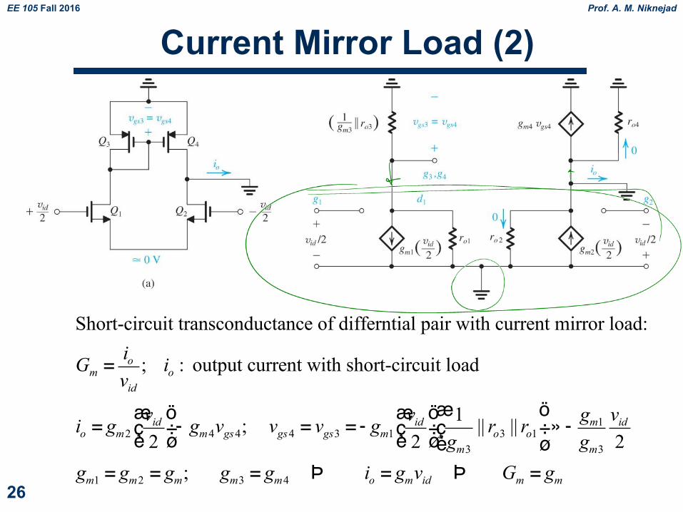
Current Mirror Load (2)
Short-circuit transconductance of differntial pair with current mirror load:
Gm =iovid
; io : output current with short-circuit load
io = gm2vid2
æèç
öø÷- gm4vgs4; vgs4 = vgs3 = - gm1
vid2
æèç
öø÷
1gm3
|| ro3 || ro1æèç
öø÷» - gm1
gm3
vid2
gm1 = gm2 = gm; gm3 = gm4 Þ io = gmvid Þ Gm = gm

EE 105 Fall 2016 Prof. A. M. Niknejad
27
Current Mirror Load (3)
Output resistance,Rout = Rop || Ron = ro4 || ro2
Ad =GmRout = gm ro4 || ro2( )RopRon
Rout

EE 105 Fall 2016 Prof. A. M. Niknejad
28
Common Mode Gain
Common mode gain (derivation skipped):
Acm » -1
2gm3RSS
CMRR = AdAcm
= gm ro4 || ro3( )×2gm3RSS
For ro4 = ro3 = ro and gm = gm3
CMRR = gmro( ) gmRSS( )