Embed Size (px)
Citation preview
Molecular Electronics: History and FundamentalsMarques-Gonzalez, S., & Low, P. (2016). Molecular Electronics: History and Fundamentals. AustralianJournal of Chemistry, 69(3), 244-253. DOI: 10.1071/CH15634
Published in:Australian Journal of Chemistry
DOI:10.1071/CH15634
Document VersionPeer reviewed version
Link to publication in the UWA Research Repository
General rightsCopyright owners retain the copyright for their material stored in the UWA Research Repository. The University grants no end-userrights beyond those which are provided by the Australian Copyright Act 1968. Users may make use of the material in the Repositoryproviding due attribution is given and the use is in accordance with the Copyright Act 1968.
Take down policyIf you believe this document infringes copyright, raise a complaint by contacting [email protected]. The document will beimmediately withdrawn from public access while the complaint is being investigated.
Download date: 10. Jun. 2018
Molecular electronics: history and fundamentals
Santiago Marqués-González,a,b Paul J. Lowa,c
a Department of Chemistry, Durham University, South Rd, Durham, DH1 3LE, UK
b Department of Chemistry, Graduate School of Science and Engineering, Tokyo
Institute of Technology, Meguro, Tokyo 152-8551, Japan
c School of Chemistry and Biochemistry, University of Western Australia, 35 Stirling
Highway, Crawley, 6009, WA, Australia.
Abstract
The increasing difficulties of meeting “Moore’s Law” rates of progress in conventional
semiconductor electronics, coupled with the advent of methods capable of measuring
the electronic properties of single molecules in a laboratory setting, has seen a surge of
activity in the field of molecular electronics over the last decade. However, the concepts
of molecular electronics are far from new, and the basic premise and ideas of molecular
electronics have been shadowing those of solid state semiconductor electronics since the
middle of the 20th Century. In this Primer Review we introduce the topic of molecular
electronics, drawing on some of the earliest expressions of the fundamental concepts,
and summarising key concepts to provide the interested reader with an entry to this
fascinating field of science and emerging technology.
1
1. Introduction
Molecular electronics is an interdisciplinary field that involves the use of
molecules as fundamental electronic components such as wires, transistors, memory
cells, and logic elements. The field, sometimes called “moletronics”,[1] is currently
attracting attention from a broad cross-section of the scientific community in response
to both fascination with the fundamental scientific challenges associated with the
measurement of the electrical properties of molecules, and manipulation of electronic
phenomena via molecular processes,[2] and growing concerns over the technological
challenges and ultimate limits facing solid state semiconductor technology.[3]
Before entering discussion, a distinction needs to be made between molecular
materials for electronics and single molecule electronics. The use of organic materials
for electronic applications in which the bulk electronic or optoelectronic response arises
from ensembles of several millions of molecules, and for which properties are measured
or observed on the macroscopic level, is at a mature stage of development and
application. The most obvious examples of molecular materials readily available in the
electronics mass market are the use of liquid crystals and organic light emitting diodes
(OLEDs) in flat video displays.[4] This sector of the electronics industry continues its
steady development driven by the promises of transparent, flexible, non-toxic, printable
electronics, with improved consumer appeal and reduced fabrication costs.
However, the field of single molecule electronics, which is the subject of this
review, can be summarised as the use of individual molecules to mimic functional
elements in electronic devices. The use of molecules as building blocks to give rise to a
more complex system is typically referred to as a the “bottom-up” approach, as opposed
to the conventional “top-down” lithographic techniques that are employed to etch small
2
features into single-crystal silicon wafers. Despite, or perhaps because of, the great
challenges the field of single molecule electronics presents, the enormous benefits of a
molecule-based “bottom-up” approach motivates the scientific community to keep
moving the field forward. For example, a typical computer microchip nowadays
contains of the order of 109 transistors in areas of about 3 cm2 with all its components
working in perfect harmony and capable of changing state in response to an input signal
at an astonishing rate and for an almost unimaginable number of cycles. The enormous
challenge for single molecule electronics lies in the development of molecular systems
that perform in some way better than, or perhaps provide an alternative function to,
these extraordinary solid-state devices.
2. Molecular and semi-conductor electronics: a brief account of an interwoven
history
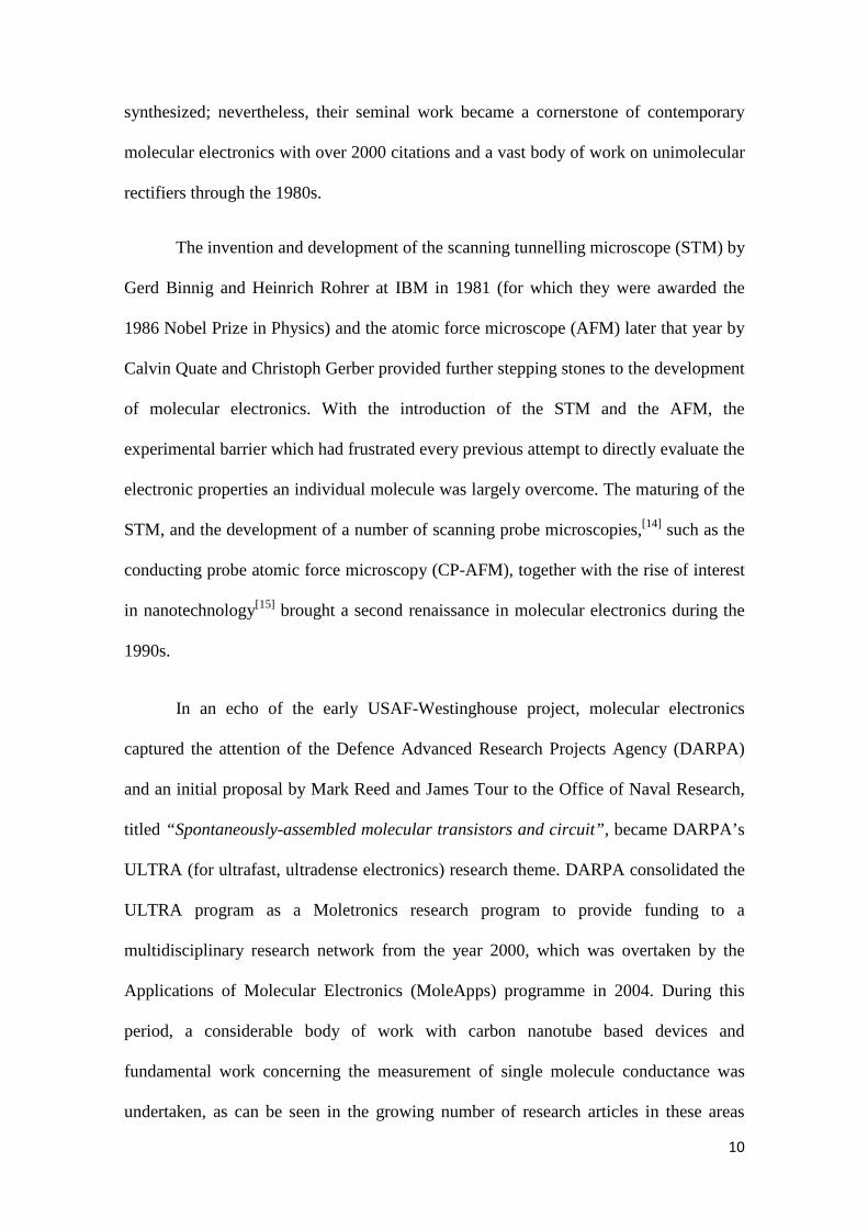
To comprehend the incentives that drive the development of molecular
electronics (Figure 1, right), it is necessary to first appreciate the evolution of the silicon
microelectronics industry (Figure 1, left).[5] The first experiments concerning the
electrical properties of semiconductor materials began early in the 19th century. The
surprising properties of these materials, such as their increased conductance when
heated or exposed to light, captured the attention of scientists and engineers of the time.
Amongst the most renowned contributors of the time are Michael Faraday, who first
reported the conductance increase with temperature in silver sulfide (1833), Alexandre-
Edmond Bequerel, father of the photovoltaic effect (1839), and Alexander Graham Bell
who in 1880 took advantage of photo-sensitivity of selenium to transmit sound over a
beam of light, inadvertently heralding the fiber-optic communications revolution of the
3
21st Century, with a remarkable invention that he named the “photophone”
(US235199A).
In spite of the potential of these early experiments, it is the development of the
solid-state transistor that might best be considered to mark the beginning of the
semiconductor revolution. Shortly after the end of World War II (1947) Walter Brattain,
John Bardeen and William Shockley of Bell laboratories discovered that by applying a
small bias to the surface of a germanium block, the current flow through a second
circuit connected to that piece of germanium could be modulated, thereby providing the
first demonstration of a solid-state transistor.
4
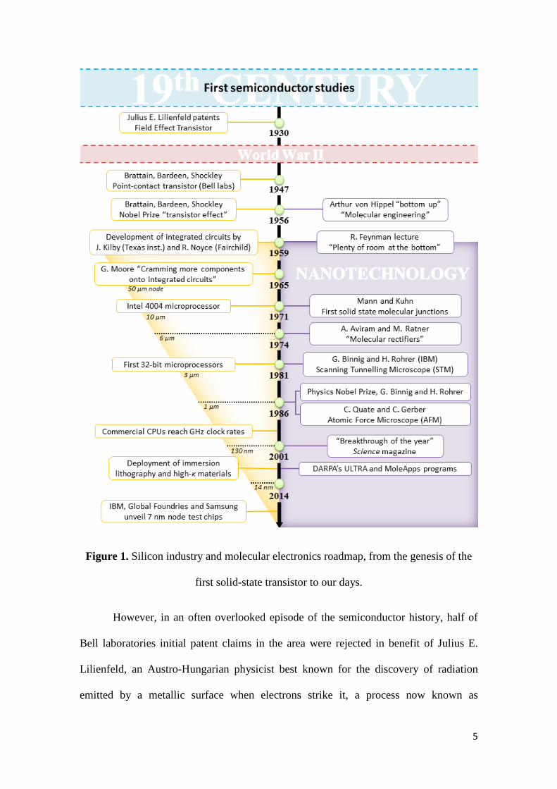
Figure 1. Silicon industry and molecular electronics roadmap, from the genesis of the
first solid-state transistor to our days.
However, in an often overlooked episode of the semiconductor history, half of
Bell laboratories initial patent claims in the area were rejected in benefit of Julius E.
Lilienfeld, an Austro-Hungarian physicist best known for the discovery of radiation
emitted by a metallic surface when electrons strike it, a process now known as
5
Lilienfeld radiation. In 1930, seventeen years before the Bell labs discovery, Lilienfeld
patented the ‘field-effect transistor’ (US1745175A). Despite his early description of the
transistor effect, Lilienfeld’s work was largely ignored by the emerging semiconductor
industry. Bell patents were finally issued for the “point-contact transistor” by Brattain
and Bardeen (US2524035A) and the “junction transistor” by Shockley (US2569347A).
In 1956, only nine years after the first transistor was built, Brattain, Bardeen and
Shockley were awarded the Physics Nobel Prize for the discovery of the transistor
effect. In recognition of Lilienfeld’s sometimes overlooked contribution to science, an
annual prize that carries his name was established in 1988 by the American Physical
Society to reward a most outstanding contribution to physics.
The 1950s was an era of frenetic activity at the Bell laboratories aligned around
the production of solid-state electronics. Parallel to the fabrication of the first
transistors, Jules Andrus and Walter L. Bond began adapting a photoengraving
technique used to print patterns onto integrated circuits to generate sophisticated designs
on silicon wafers. The solid-state transistor and photolithographic process, together with
the serendipitous discovery in 1955 of silicon oxide masking by Carl Frosch, also at
Bell, marked the start point for the modern monolithic microelectronics industry.
However, the same year that the Physics Nobel Prize was awarded for the discovery of
the transistor effect (1956), a German physicist named Arthur von Hippel, then working
at the Massachusetts Institute of Technology, proposed a completely different approach:
“Instead of taking prefabricated materials and trying to devise engineering
applications consistent with their macroscopic properties, one builds
materials from their atoms and molecules for the purpose at hand ...”[6]
6
The notion of “molecular engineering” introduced by von Hippel might be the
first expression of the “bottom-up” approach and could be regarded as the initial
expression of the concept of molecular electronics. von Hippels’s ideas were quickly
embraced by the Westinghouse Electric company,[7] and the US Air Force (USAF). At
that time, the airborne electronic equipment was growing increasingly complex and
vulnerable to failure, as aircraft began flying faster and higher. In 1959 the USAF
decided to invest US$2 million in a joint USAF-Westinghouse research program for the
development of molecular electronics as a possible solution to their problems. Their
research proposal “Molecular Electronics – Dendritic Approach” proved successful
enough to be funded until 1962, although the research program was ultimately
abandoned due to severe manufacturing issues and the rapid progress of the silicon
electronics technology. Coincidently, also in 1959 Jack Kilby at Texas Instruments, and
Robert Noyce at Fairchild Camera, had developed a method to integrate even more of
the individual components to create a ‘solid circuit’. The ability to print and wire
several electronic components on a silicon substrate, coupled with reduction in the size
of components promised to reduced production costs and increase reliability. The
importance of their work was recognized later in 2000 when Kilby was awarded the
Physics Nobel Prize for his contribution in the invention of the integrated circuit.
The desire for smaller, faster, more highly functional electronic components
gave rise to the rapid post-war evolution of the silicon industry, led by development of
the integrated circuit and economic drivers. In 1965, a marketing research paper
“Cramming more components onto integrated circuits” was published by Gordon E.
Moore, then at Fairchild Semiconductors.[8] In this study, Moore noted the doubling of
component density every two years on electronic circuits, and projected that such rates
of progress might be possible until 1975 (!). Only three years later, in 1968, Moore,
7
together with Noyce, founded the Intel Corporation, and in 1971, the Intel 4004
processor was introduced, with over 2000 transistors built on a silicon monolith the size
of a fingernail. The journey towards the evolution of consumer electronics and the
multi-billion dollar semiconductor industry had begun. As semiconductor fabrication
techniques evolved, Moore’s expression of component density doubling every two years
became a self-imposed growth target for the semiconductor industry. The desire to
maintain this rate of progress, typically referred to as “Moore’s Law”, has driven the
relentless miniaturization efforts of the semiconductor industry for five decades.
In contrast, the ideas of molecular electronics technology laid largely fallow
until the 1970s, when a second phase of interest swept the community. Again in 1959,
not long before Moore’s seminal expression of the rates of progress in the
semiconductor industry based on economic considerations, Richard Feynman gave his
now widely celebrated lecture to the American Physical Society at CalTech titled
“There’s plenty of room at the bottom” in which he challenged the whole scientific
community to push the miniaturization limits.[9] For many, the ideas Feynman exposed
in that lecture are the starting point of nanoscience and nanotechnology. In a remarkable
piece of foresight and imagination Feynman succinctly drew together the threads of
both the fast emerging microelectronics industry with a future molecular electronic
technology by noting that, en route to an ultimate miniaturisation of technology,
chemical synthesis allows for the precise organisation of matter within a molecular
framework.
At that time, although chemical synthesis was (relatively) well developed,
establishing electrical contacts across individual molecules was not possible; however
intramolecular electron transfer was being increasingly studied in solution, with
considerable interest in using the characteristic spectroscopic profiles associated with
8
‘mixed valence’ complexes and compounds, led by the seminal work of Taube, Marcus
and Hush.[10] Indeed, the use of mixed-valence systems as models for molecular
electronics components continues to this day, although the neglect of the surface-
molecule interface in these models is noted.[11]
The first direct measurements of through molecule conductance were reported in
1971 when Mann and Kuhn[12] prepared a series of well-ordered fatty acid monolayers
employing the Langmuir-Blodgett (LB) technique, and succeeded in sandwiching them
between metal electrodes and measuring the electrical properties of the systems. Their
studies revealed an exponential decay of the conductivity with the molecular length.
Molecular electronic concepts began to take further formative and conceptual steps
through the 1970s. In 1974, Ari Aviram (IBM) and Mark Ratner (New York University)
started working on a theory of electron transfer through single organic molecules. Their
efforts crystallized in a now-famous article titled “Molecular Rectifiers”.[13] In that
document, Aviram and Ratner described for the first time the use of a molecule with a
modular design based on fragments familiar to chemists as an electronic component
(Chart 1).
NC CN
NC CN
S
S
S
S
Acceptor
Donor
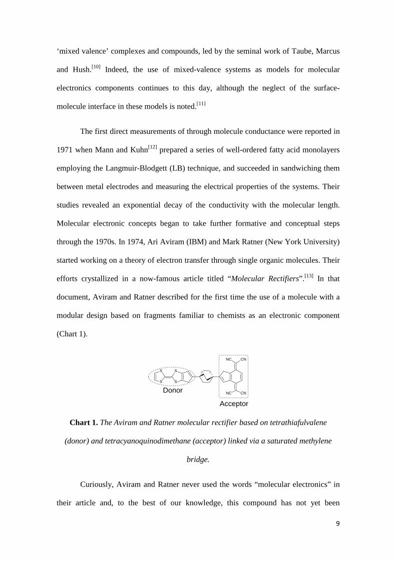
Chart 1. The Aviram and Ratner molecular rectifier based on tetrathiafulvalene
(donor) and tetracyanoquinodimethane (acceptor) linked via a saturated methylene
bridge.
Curiously, Aviram and Ratner never used the words “molecular electronics” in
their article and, to the best of our knowledge, this compound has not yet been
9
synthesized; nevertheless, their seminal work became a cornerstone of contemporary
molecular electronics with over 2000 citations and a vast body of work on unimolecular
rectifiers through the 1980s.
The invention and development of the scanning tunnelling microscope (STM) by
Gerd Binnig and Heinrich Rohrer at IBM in 1981 (for which they were awarded the
1986 Nobel Prize in Physics) and the atomic force microscope (AFM) later that year by
Calvin Quate and Christoph Gerber provided further stepping stones to the development
of molecular electronics. With the introduction of the STM and the AFM, the
experimental barrier which had frustrated every previous attempt to directly evaluate the
electronic properties an individual molecule was largely overcome. The maturing of the
STM, and the development of a number of scanning probe microscopies,[14] such as the
conducting probe atomic force microscopy (CP-AFM), together with the rise of interest
in nanotechnology[15] brought a second renaissance in molecular electronics during the
1990s.
In an echo of the early USAF-Westinghouse project, molecular electronics
captured the attention of the Defence Advanced Research Projects Agency (DARPA)
and an initial proposal by Mark Reed and James Tour to the Office of Naval Research,
titled “Spontaneously-assembled molecular transistors and circuit”, became DARPA’s
ULTRA (for ultrafast, ultradense electronics) research theme. DARPA consolidated the
ULTRA program as a Moletronics research program to provide funding to a
multidisciplinary research network from the year 2000, which was overtaken by the
Applications of Molecular Electronics (MoleApps) programme in 2004. During this
period, a considerable body of work with carbon nanotube based devices and
fundamental work concerning the measurement of single molecule conductance was
undertaken, as can be seen in the growing number of research articles in these areas
10
published during the second half of the 1990s. A series of quite remarkable
achievements in 2001 including the creation of carbon nanotube based transistors,[16]
switchable devices from rotaxanes embedded between n-type polysilicon and Ti/Al
electrodes [17] and reports of 16-bit memory from similar rotaxanes in cross-bar
junctions lead the Science magazine to describe ‘Nanoelectronics’ and the construction
of these rudimentary circuits the breakthrough of the year in 2001.[18] In recent years,
these concepts have evolved and devices as complex as 160-kb rotaxane-based cross-
bar memories have been described. [19]
Against this background of steady progression in molecular electronics, the
semiconductor industry has pushed relentlessly forward at Moore’s Law pace until the
present day.[20] The miniaturization race required remarkable innovations in
microarchitecture designs such as 3D transistors (tri-gate or FinFET),[21] technical
developments such as immersion lithography and double patterning, and the use of
exotic high-κ dielectrics to alleviate tunnelling issues of gate-insulators of only a few
atoms thick.[22] However, the difficulties involved in maintaining Moore’s Law rates of
miniaturization below the 20 nm barrier is perhaps best illustrated by the delayed
deployment of the 14 nm chips (Intel Broadwell, 2015). Whilst a miss-step in Intel’s
production schedule and failure to meet its long standing 12-18-month ‘tick-tock’
schedule of chip refresh (tick = shrinking of the process technology; tock = new
microarchitecture), may not seem a major economic or technological concern, this
missed production window is an indication of the growing difficulties that conventional
semiconductor fabrication methods are now facing. In fact, the challenges associated
with manufacturing advanced electronic circuits are now so great that in the
international community has been forced to re-write Moore’s Law:
After 2013, the Moore’s Law rate of on-chip transistors slows to double every three
11
years.[23]
Nevertheless, the miniaturization race continues, as it was recently proven by IBM,
Global Foundries and Samsung research alliance, with the development of the first 7 nm
node test chips at the SUNY Polytechnic Institute’s College of Nanoscale Science and
Engineering. This astonishing feat required several industry-first innovations such as the
fabrication of Si-Ge transistor channels, extreme ultraviolet lithography, and allegedly
quadruple patterning.
As the semiconductor industry approaches the physical limits of solid-state
materials, molecular electronics is entering something of a third era, this time supported
by shared academic and industrial interest, with an appreciation of the need to solve
fundamental problems in order to reach a hybrid electronics technology in which
molecular systems serve as a viable material within solid state frameworks. However,
the complex experimental set-up required to determine the electrical properties of a
single molecule has historically been, and to some extent still is, one of the most
important obstacles to the exploration of fundamental concepts in molecular electronics
and advancement towards a viable technology. Nevertheless, the invention of the STM
and AFM and improvements in nanofabrication, now present us with a number of
methods that allow the formation of molecular junctions in order to study their physical
properties and electronic performance have been firmly established.[24] The main aim of
these methods is to assemble either one or a small number of molecules between two
metallic electrodes to create a junction, which in turn allows the electronic properties of
the sandwiched molecules to be measured.[25] In the remainder of this article we turn
attention to these molecular junctions, and explore the basic processes that underpin the
electrical properties of molecules within electrode gaps.
12
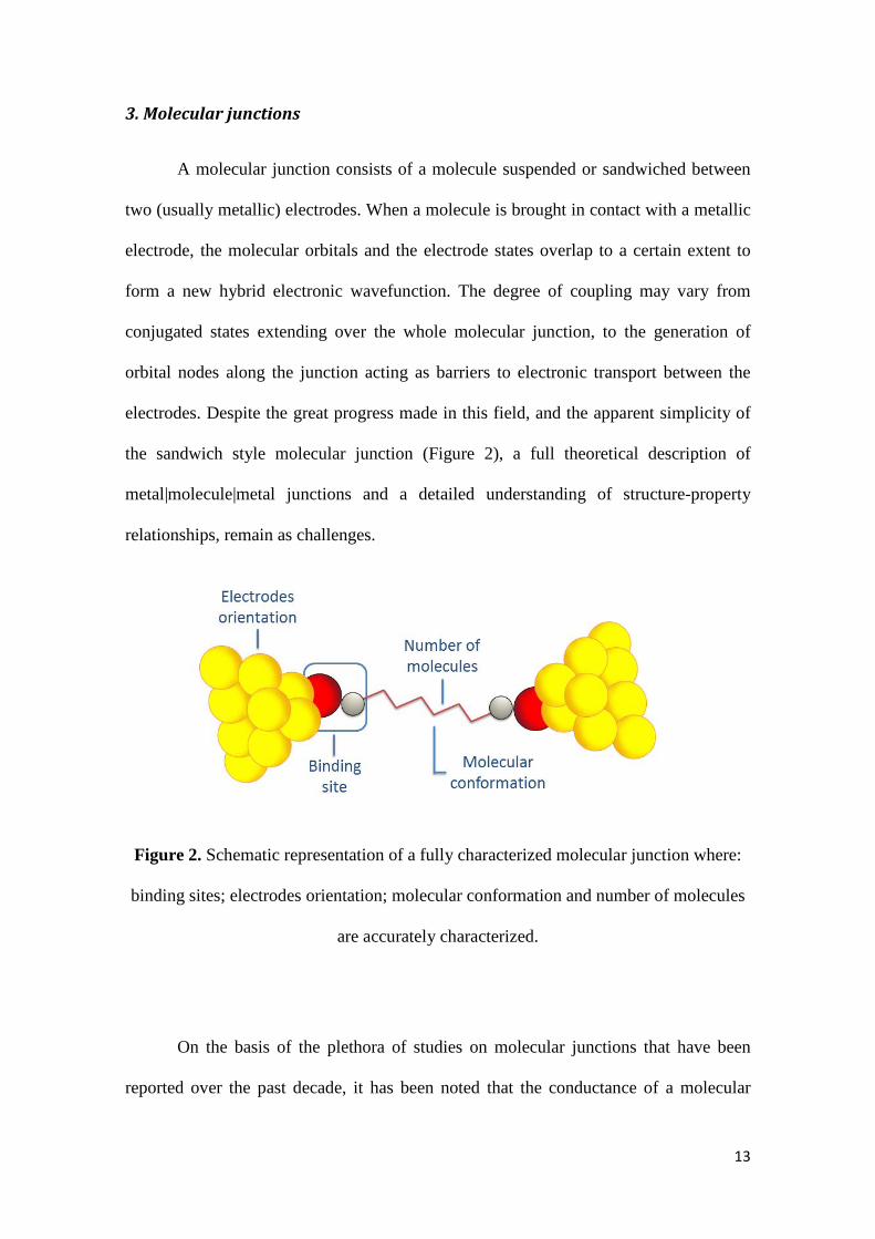
3. Molecular junctions
A molecular junction consists of a molecule suspended or sandwiched between
two (usually metallic) electrodes. When a molecule is brought in contact with a metallic
electrode, the molecular orbitals and the electrode states overlap to a certain extent to
form a new hybrid electronic wavefunction. The degree of coupling may vary from
conjugated states extending over the whole molecular junction, to the generation of
orbital nodes along the junction acting as barriers to electronic transport between the
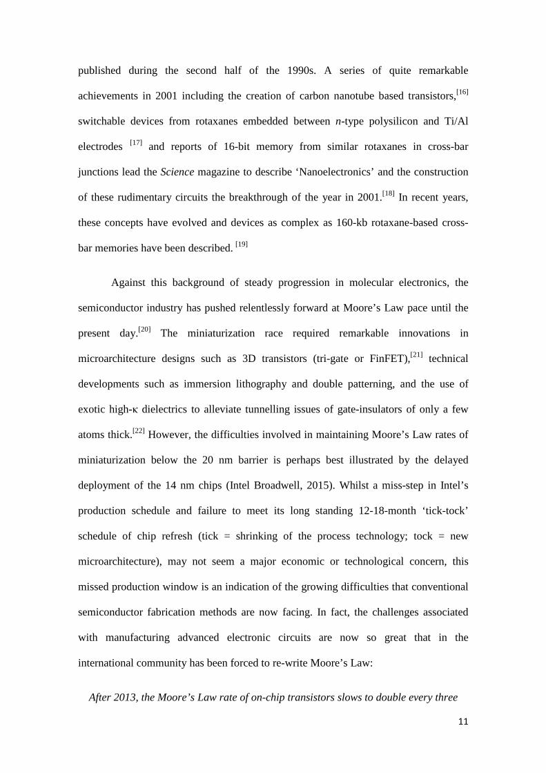
electrodes. Despite the great progress made in this field, and the apparent simplicity of
the sandwich style molecular junction (Figure 2), a full theoretical description of
metal|molecule|metal junctions and a detailed understanding of structure-property
relationships, remain as challenges.
Figure 2. Schematic representation of a fully characterized molecular junction where:
binding sites; electrodes orientation; molecular conformation and number of molecules
are accurately characterized.
On the basis of the plethora of studies on molecular junctions that have been
reported over the past decade, it has been noted that the conductance of a molecular
13
junction can be affected by several factors such as: the structure and degree of
conjugation of the molecular bridge;[26] the nature of the linker group and its
geometry;[27] the junction geometry (tilt angles and gap size);[28] and the electronic
character of substituents on the molecular backbone.[29]
Much of the early work in single molecule studies was focused on the molecular
backbone assuming that any other factor would have a small influence in the junction
electronic performance. Particularly large contributions to this field have come from
studies of symmetrically and unsymmetrically substituted linear oligo(phenylene-
ethynylene) (OPE) derivatives, [30] including organometallic analogues. [31] These highly
conjugated derivatives, sometimes referred to as “Tour wires” due to the pioneering
studies of these molecules by J. M. Tour,[32] have been of significant interest in many
different fields of chemistry and physics due to their exceptional properties.[33] The
modular synthesis of OPEs,[34] and good single molecule conductance ensure that these
systems merit particular attention.[26b, 35]
However, despite the great interest in the design of conjugated wire-like
backbones for use in molecular electronic components, it is now agreed that the metal-
molecule interface, and therefore the molecular anchoring group, have a great influence
on the global junction behaviour.[27a, 27b] This area of research has been largely
dominated by the thiolate linker that, due to its ability to self-assemble on gold has
provided a strong test-bed to study the electrical properties of single molecules and
ensembles.[36] However, several potential disadvantages have been reported to the use of
thiols as molecular linkers. The thiolate-gold bond has a strength similar to that of the
gold-gold bond resulting on the electrode surface modification.[37] In addition, at room
temperature, stochastic switching of the junction conductance has been observed,
ascribed to the mobility of the chemisorbed contacts.[38] The free thiols also tend to
14
oxidise to give dithiolates, often requiring the use of protective groups during their
synthesis. Due to these difficulties and the influence of the linker on the junction
properties, the development of alternative contacts has become an area of great research
activity and several alternative linkers to thiols have been proposed.[27c-f, 39]
In addition to the linker, the exact separation between the two electrodes when
the molecular bridge is formed can have a pronounced influence in the junction
conductance. This is extremely relevant to the development of molecular electronic
devices that can show a considerable range of contact-gap separation. Haiss et al.
demonstrated that the molecular conductance can be measured as a function of electrode
gap to sub-nanometre precision.[28a] More recently, the effect of the junction gap was
also studied for a series of rigid molecular wires.[28b] In those studies, a substantial
conductance increase was found as the gap between the electrodes was closed. DFT
studies supported those results proving the significant influence of the molecular tilt
angle in the junction conductance.[28a]
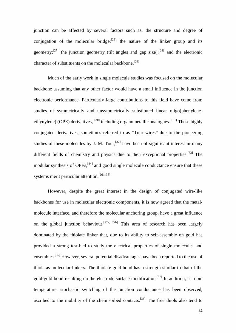
A simplified electronic description of a molecular junction involving two
electrodes bridged by a molecule can be seen in Figure 3. Both electrodes are described
as a continuum of energy levels filled up to a given energy level (Fermi level), the
energy symmetry between both electrodes is broken by the applied bias. On the other
hand, the bridging molecule is characterized by discrete energy levels filled up to the
HOMO. Importantly, the orbital alignment relative to the electrode Fermi level is
directly characteristic of each molecular junction and dependant on several factors such
as: the nature of the molecular bridge;[40] the nature of the metal-molecule
interaction;[27e] the electronic and conformational changes induced by the charge
transfer;[41] environmental effects[25b] and redox state. [25b, 42]
15
Figure 3. Simplified description of the electronic diagram in a molecular junction.
Charge transport in molecules contacted by macroscopic electrodes is best
described by the Landauer formalism. In this description electrons are treated as waves
that can be reflected or transmitted through the molecular bridge. According to the
Landauer formalism the conductance G of a molecular junction can be calculated
(Equation 1).
𝐺𝐺 = 2𝑒𝑒2
ℎ∑ 𝑇𝑇𝑛𝑛𝑛𝑛 Equation 1
where e is the electron charge, h is Planck’s and Tn are the transmission coefficients of
the individual transport channels. According to this expression, the conductance of a
system G, is the summation of all possible individual transmission channels. Perhaps
the most relevant implication of this equation is that conductance at the molecular level
is quantized. For a perfect coupling i.e. ballistic conductors (Tn = 1), the conductance
can only increase or decrease in units of the quantum of conductance G0 = 2e2/h ~
77481 nS. It is important to clarify that the Landauer formalism does not imply that the
conductance of any system must be an integer of G0 however it defines the maximum
16
conductance for a single channel as the G0. Transmission coefficients Tn typically take
values smaller than the unity and several transport channels coexist to give the system
conductance. Conductance values for single molecules are orders of magnitude smaller
than G0 typically ranging from (10-5 - 10-1) G0.
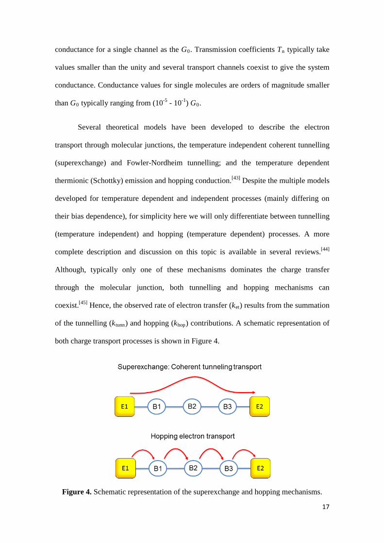
Several theoretical models have been developed to describe the electron
transport through molecular junctions, the temperature independent coherent tunnelling
(superexchange) and Fowler-Nordheim tunnelling; and the temperature dependent
thermionic (Schottky) emission and hopping conduction.[43] Despite the multiple models
developed for temperature dependent and independent processes (mainly differing on
their bias dependence), for simplicity here we will only differentiate between tunnelling
(temperature independent) and hopping (temperature dependent) processes. A more
complete description and discussion on this topic is available in several reviews.[44]
Although, typically only one of these mechanisms dominates the charge transfer
through the molecular junction, both tunnelling and hopping mechanisms can
coexist.[45] Hence, the observed rate of electron transfer (ket) results from the summation
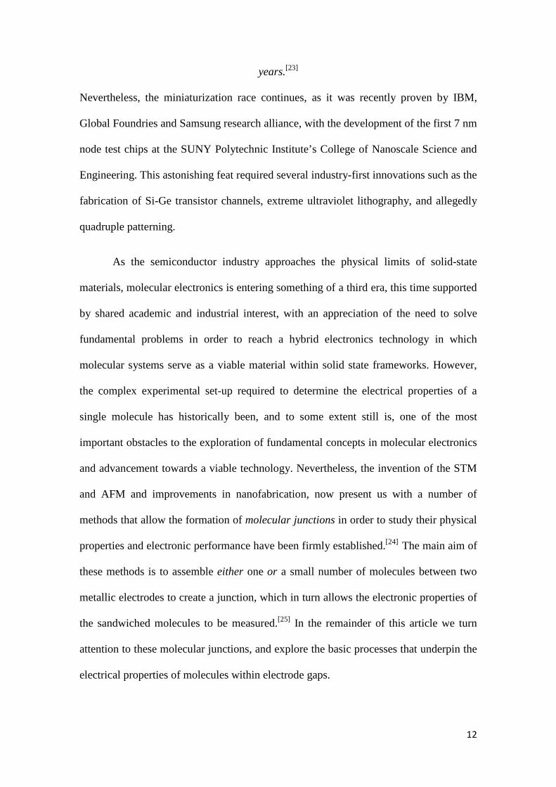
of the tunnelling (ktunn) and hopping (khop) contributions. A schematic representation of
both charge transport processes is shown in Figure 4.
Figure 4. Schematic representation of the superexchange and hopping mechanisms.
17
The super-exchange mechanism is based on the probability of an electron
traversing an energy barrier coherently i.e in the absence of inelastic scattering events.
In this case, the charge transfer takes place in one step through the molecular orbitals of
the bridging molecule. Hence, the charge carrier is considered not to reside in the
orbitals of the bridging molecular wire for a significant space of time. It is important to
note that, the electron transference kET is enhanced by the molecular orbitals increasing
the probability of through-bond tunnelling over trough-space tunnelling. In this scenario
the energy barrier is set by the energetically higher electronic states of the bridge
compared to those of the electron source. The electron transport rate kET for the super-
exchange mechanism can be calculated using Equation 2
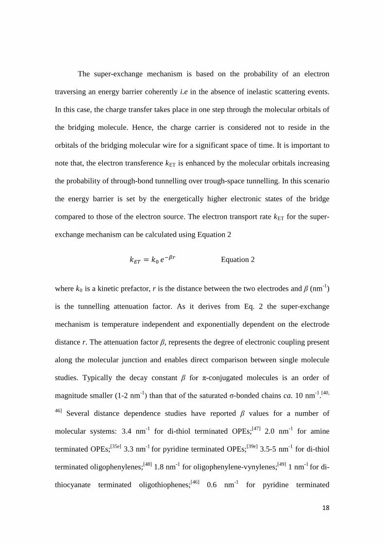
𝑘𝑘𝐸𝐸𝐸𝐸 = 𝑘𝑘0 𝑒𝑒−𝛽𝛽𝛽𝛽 Equation 2
where k0 is a kinetic prefactor, r is the distance between the two electrodes and β (nm-1)
is the tunnelling attenuation factor. As it derives from Eq. 2 the super-exchange
mechanism is temperature independent and exponentially dependent on the electrode
distance r. The attenuation factor β, represents the degree of electronic coupling present
along the molecular junction and enables direct comparison between single molecule
studies. Typically the decay constant β for π-conjugated molecules is an order of
magnitude smaller (1-2 nm-1) than that of the saturated σ-bonded chains ca. 10 nm-1.[40,
46] Several distance dependence studies have reported β values for a number of
molecular systems: 3.4 nm-1 for di-thiol terminated OPEs;[47] 2.0 nm-1 for amine
terminated OPEs;[35e] 3.3 nm-1 for pyridine terminated OPEs;[39e] 3.5-5 nm-1 for di-thiol
terminated oligophenylenes;[48] 1.8 nm-1 for oligophenylene-vynylenes;[49] 1 nm-1 for di-
thiocyanate terminated oligothiophenes;[46] 0.6 nm-1 for pyridine terminated
18
oligoynes;[39b] as opposed to 9.4 nm-1 for saturated di-thiol terminated alkyls[48a] and the
24-40 nm-1 for vacuum.[50] It is important to note that, the attenuation factor β not only
depends on the orbital delocalization of the molecular backbone but on the entire
molecular junction, including the binding sites and the electrode shape and material (i.e.
the measuring technique).[49a] However, due to the exponential distance dependence of
the superexchange mechanism, coherent tunnelling is only effective for distances under
2.5 nm. The charge hopping mechanism is believed to dominate for longer bridges (ca.
> 3 nm).
Contrary to the super-exchange mechanism, in the case of charge hopping, the
electron traversing the molecular wire is localized for a short time before moving to the
next bridge site until it crosses trough the molecular junction.[49b, 51] The hopping
conduction mechanism is more likely to be present in molecular junctions where the
Fermi levels of the metallic contacts lie close in energy to the molecular bridge frontier
orbitals.[43] Importantly, significant nuclear motion is involved in this transport process
as vibrational relaxation takes place at each bridge site. Consequently, the distance
dependence of charge hopping is less marked, i.e. inversely proportional to distance
(Ohmic) (Equation 3) (although other relationships are also known (e.g. kET = khopN-2,
where N is the number of hopping stations in the bridge)).[45] In addition, due to the
vibrational relaxation processes involved the hopping mechanism is temperature
dependant.[43, 45]
𝑘𝑘𝐸𝐸𝐸𝐸 = 𝑘𝑘ℎ𝑜𝑜𝑜𝑜 ∝ 1/𝑟𝑟 Equation 3
In order to experimentally determine the transport process ruling in a given
molecular junction, two electrical measurements are typically performed: the length
dependence of the molecular conductance and the temperature dependence of the I-V
19
profile. These experiments also exclude the possibility of artefacts such as metallic
filaments or interface effects being the source of the electrical properties registered.
However, the determination of the charge transport mechanism can sometimes be
difficult. For example, a pronounced temperature dependence was reported for the
conductance of alkanedithiols attributed to changes in the distribution of the molecular
conformers.
The coexistence of both tunnelling and hopping mechanisms was first reported
by Wasielewski and Ratner.[52] In their work, the recombination rate of several
photoexcited Donor-Bridge-Acceptor (D-B-A) complexes featuring p-phenylene-
vinylene oligomeric bridges (n = 1 - 5) was studied. Notably, a less marked distance
dependence was found for those molecular bridges with sizes over 2.4 nm that was
attributed to a change in the transport mechanism from superexchange (n = 1 - 2) to
hopping (n = 3 - 5). Choi and co-workers reported a similar behaviour for
phenyleneimine oligomers (n = 1 – 10) in solid state CP-AFM studies.[53] Those results
confirmed the coexistence of both transport mechanisms in the solid state. In this case,
transport mechanism was reported to change from tunnelling to hopping for molecular
wires over 4 nm in size (n = 6 - 10). Despite the great experimental complexity of these
experiments, a number of similar studies have been reported recently confirming the
coexistence of both mechanisms.[35e, 39e, 54] Although in first instance the charge hopping
mechanism and its weaker distance dependence should allow long distance charge
transport, which makes it more attractive for potential electronic application, the
tunnelling mechanism is still intriguing the scientific community. For instance, recent
studies indicate that tunnelling-energy gap effects can differentiate the distance
dependence of energy-storing charge-separation reactions from energy-wasting
20
recombination processes.[50b] Hence further understanding of the tunnelling mechanism
may provide an additional way to obtain long-living charge-separated states.
4.2 Relationships between electron transfer rates and molecular conductance.
As the number of single molecule studies increases, several theoretical studies
have investigated the relation between the electron transfer rates (kDA) obtained from
the in-solution studies and the molecular conductance (G) obtained for molecular
junctions.[55] Despite the fundamental differences behind the two physical systems both
processes depend on quantum tunnelling to carry the charge through the molecular
bridge.[44b, 56] Hence, the conduction profile of a given system and its electron transfer
properties must be closely related.[55a] It is important to bear in mind that, because of the
tunnelling regime there is always an Ohmic behaviour region near zero bias. On the
basis of this similarity first noted by Nitzan,[55a, 57] the relation between the rate constant
kAD and conductance G is shown in Equation 4
𝐺𝐺 ≈ 𝑒𝑒2
Γ𝐷𝐷Γ𝐴𝐴𝐹𝐹𝑘𝑘𝐷𝐷𝐷𝐷 Equation 4
where e is the electron charge, and the Г factors are the inverse lifetimes of an electron
on the donor and acceptor states once the molecular junction is formed, and F is the
Marcus thermally averaged Franck-Condon factor dependant of reorganization energy
and temperature. However this relation is only applicable for the simple case of thermal,
non-adiabatic electron transfer in those junctions where the molecular electronic
structure is not greatly affected by the metal-molecule interaction. A rough estimation
of this relation for a junction with typical magnitudes of reorganization energy and
metal-molecule coupling was done by Nitzan leading to G(S) ~ 10-17 kDA (s-1).[55a]
Despite the fact that this theoretical model was first developed for the tunnelling
21
mechanism, it was later extended to the hopping mechanism.[57] For those cases where
the charge transfer takes place through a large number of bridge sites the relation
between G and kDA was found to be
𝐺𝐺 ≈ 𝑒𝑒2
𝑘𝑘𝐵𝐵𝐸𝐸𝑒𝑒−
∆𝐸𝐸𝑘𝑘𝐵𝐵𝑇𝑇 𝑘𝑘𝐷𝐷𝐷𝐷 Equation 5
where kB is the Boltzmann constant, e is the electron charge and ΔE is the difference
between the activation energies involved. Interestingly at T = 300 K, for those cases
where ΔE ≤ kBT, Eq 1-14 can be simplified as G(S) ~ (5· 10-18) kDA (s-1) remarkably
similar to the numerical estimate obtained for the coherent tunnelling mechanism.
Recently, Wierzbinski and co-workers reported the first experimental study of
this relationship.[54b] In their work, they evaluated the correlation between molecular
conductance and electrochemical rate constants for alkanes and nucleic acid oligomers
as a function of length, structure and charge transport. Interestingly, contrary to the
linear correlation theoretically proposed by Nitzan a power law correlation was found
between G and kDA for each molecular bridge studied. The deviation from the linear
relation was attributed to charge-transfer energy barriers and bridge dephasing. In
situations where multiple mechanisms can coexist, these factors can lead to differences
between the distance dependence of kDA and G. Generally speaking, these results show
the relative propensity of different chemical species to transmit charge differently in
electrochemical measurements as opposed to molecular junctions.
4. Conclusion and future prospects in molecular electronics
Since its inception some 60 years ago the field of molecular electronics has
surged, ebbed, and surged with conceptual, technical and scientific advances. The great
22
advances in our understanding of the unique and complex nature of charge transport at
the molecular level, together with a growing and increasingly recognised industrial
need, may, perhaps finally, see the potential of molecular electronics realised.
Through the wider access to the experimental tools that allow single molecule
measurements, many new charge transport phenomena beyond the simple ballistic
electron transport have been identified. Amongst those phenomena, molecular rectifying
(redox, thermal or mechanic), quantum-interference, spintronics and optoelectronics are
now being actively pursued, and open avenues for exploration of both organic
compounds and metal complexes. In addition, theoretical models and computational
methods based on the non-linear Green’s function (NLGF) are providing the theoretical
base required to fully understand the transport process at the nano-scale. A full
description of the theoretical rules that drive the molecular conduction is of great
importance as it would lead to molecular behaviour prediction and therefore to a
rational design of the molecules.
Molecular electronics seems predestined to converge with the highly developed
semiconductor industry, in a curious reunification of ideas shared a common heritage
and conceptual beginning. The great effort now being devoted to increase the
compatibility of molecular electronics with the fabrication methods employed by the
semiconductor industry heralds a new initiative in realising a true molecular electronics
technology. [23]
Computing with molecules as circuit building blocks is an exciting
concept with several desirable advantages over conventional circuit
elements. Because of their small size, very dense circuits could be
built, and bottom-up self-assembly of molecules in complex structures
23
could be applied to augment top-down lithography fabrication
techniques. As all molecules of one type are identical, molecular
switches should have identical characteristics, thus reducing the
problem of variability of components. However, the success of
molecular electronics depends on our understanding of the
phenomena accompanying molecular switching, where currently
many questions remain.
The obstacles to this goal should be seen as challenges for the scientific
community, acting as motivation and defining the long-term goals of the field. In the
words of Heath and Ratner,[58] on the molecular electronics horizon should be placed a
very robust, energy-efficient, connected to the outside world, computational platform
based on molecular electronics with a bit density of 1012 cm-2. The great advances
needed to accomplish that goal, would make it hard to believe that an electronic device
will be the most significant result of such an effort.
1.6. References
[1] K. S. Kwok, J. C. Ellenbogen, Materials Today 2002, 5, 28. [2] (a) F. Chen, N. J. Tao, Accounts of Chemical Research 2009, 42, 429; (b) R. M. Metzger, Journal of Materials Chemistry 2008, 18, 4364.
24
[3] (a) R. K. Cavin, P. Lugli, V. V. Zhirnov, Proceedings of the IEEE 2012, 100, 1720; (b) A. Huang, Spectrum, IEEE 2015, 52, 43; (c) N. Collaert, A. Alian, H. Arimura, G. Boccardi, G. Eneman, J. Franco, et al., Microelectronic Engineering 2015, 132, 218. [4] (a) I.-C. Khoo, I. Wiley, Liquid crystals 2007 (Wiley-Interscience: Hoboken, N.J., USA); (b) A. P. Kulkarni, C. J. Tonzola, A. Babel, S. A. Jenekhe, Chemistry of Materials 2004, 16, 4556; (c) H. Sasabe, J. Kido, Chemistry of Materials 2010, 23, 621; (d) C. Zhong, C. Duan, F. Huang, H. Wu, Y. Cao, Chemistry of Materials 2010, 23, 326. [5] H. Choi, C. C. M. Mody, Social Studies of Science 2009, 39, 11. [6] A. von Hippel, Science 1956, 123, 315. [7] E. A. Sack, D. A. Lewis, IEEE Annals of the History of Computing 2012, 34, 74. [8] G. E. Moore, Electronics Magazine 1965, 38, 8. [9] (a) 'Plenty of room' revisited [Editorial], Nature Nanotech. 2009, 4, 781; (b) R. P. Feynman, Caltech Engineering and Science 1960, 23:5, 22. [10] (a) M. B. Robin, Inorganic Chemistry 1962, 1, 337; (b) P. Day, Inorganic Chemistry 1963, 2, 452; (c) D. Culpin, P. Day, P. R. Edwards, R. J. P. Williams, Chemical Communications (London) 1965, 450; (d) C. Creutz, H. Taube, Journal of the American Chemical Society 1969, 91, 3988; (e) G. C. Allen, N. S. Hush. in Progress in Inorganic Chemistry 2007, pp. 357-389 (John Wiley & Sons, Inc.: ; (f) P. Day, N. S. Hush, R. J. H. Clark, Philosophical Transactions of the Royal Society A: Mathematical, Physical and Engineering Sciences 2008, 366, 5. [11] J.-P. Launay, Coordination Chemistry Reviews 2013, 257, 1544. [12] B. Mann, H. Kuhn, Journal of Applied Physics 1971, 42, 4398. [13] A. Aviram, M. A. Ratner, Chemical Physics Letters 1974, 29, 277. [14] R. J. Hamers, The Journal of Physical Chemistry 1996, 100, 13103. [15] Y. Xia, J. A. Rogers, K. E. Paul, G. M. Whitesides, Chemical Reviews 1999, 99, 1823. [16] H. W. C. Postma, T. Teepen, Z. Yao, M. Grifoni, C. Dekker, Science 2001, 293, 76. [17] C. P. Collier, J. O. Jeppesen, Y. Luo, J. Perkins, E. W. Wong, J. R. Heath, et al., Journal of the American Chemical Society 2001, 123, 12632. [18] R. F. Service, Science 2001, 294, 2442. [19] J. E. Green, J. Wook Choi, A. Boukai, Y. Bunimovich, E. Johnston-Halperin, E. DeIonno, et al., Nature 2007, 445, 414. [20] S. E. Thompson, S. Parthasarathy, Materials Today 2006, 9, 20. [21] F. Monnier, F. o. Turtaut, L. Duroure, M. Taillefer, Organic Letters 2008, 10, 3203. [22] (a) L. Manchanda, M. D. Morris, M. L. Green, R. B. van Dover, F. Klemens, T. W. Sorsch, et al., Microelectronic Engineering 2001, 59, 351; (b) H. Wong, H. Iwai, Microelectronic Engineering 2006, 83, 1867; (c) R. L. McCreery, H. Yan, A. J. Bergren, Physical Chemistry Chemical Physics 2013, 15, 1065. [23] J. Luo, M. Liu, Q. Zhao, J. Zhao, Y. Zhang, L. Tan, et al., Electrochimica Acta 2010, 56, 454. [24] (a) B. A. Hylke, B. Bert de, Journal of Physics: Condensed Matter 2008, 20, 013001; (b) H. Haick, D. Cahen, Accounts of Chemical Research 2008, 41, 359. [25] (a) R. L. McCreery, A. J. Bergren, Advanced Materials 2009, 21, 4303; (b) R. J. Nichols, W. Haiss, S. J. Higgins, E. Leary, S. Martin, D. Bethell, Physical Chemistry Chemical Physics 2010, 12, 2801. [26] (a) M. Mayor, C. von Hänisch, H. B. Weber, J. Reichert, D. Beckmann, Angewandte Chemie International Edition 2002, 41, 1183; (b) K. Liu, X. Wang, F. Wang, ACS Nano 2008, 2, 2315. [27] (a) S. Hong, R. Reifenberger, W. Tian, S. Datta, J. I. Henderson, C. P. Kubiak, Superlattices and Microstructures 2000, 28, 289; (b) S.-H. Ke, H. U. Baranger, W. Yang, Journal of the American Chemical Society 2004, 126, 15897; (c) F. Chen, X. Li, J. Hihath, Z. Huang, N. Tao, Journal of the American Chemical Society 2006, 128, 15874; (d) Z. L. Cheng, R. Skouta, V. H., J. R. Widawsky, S. Schneebeli, W. Chen, et al., Nat Nano 2011, 6, 353; (e) M. Frei, S. V. Aradhya, M. S. Hybertsen, L. Venkataraman, Journal of the American Chemical Society 2012,
25
134, 4003; (f) T. A. Su, J. R. Widawsky, H. Li, R. S. Klausen, J. L. Leighton, M. L. Steigerwald, et al., Journal of the American Chemical Society 2013, 135, 18331. [28] (a) W. Haiss, C. Wang, I. Grace, A. S. Batsanov, D. J. Schiffrin, S. J. Higgins, et al., Nat Mater 2006, 5, 995; (b) W. Haiss, C. Wang, R. Jitchati, I. Grace, S. Martín, A. S. Batsanov, et al., Journal of Physics: Condensed Matter 2008, 20, 374119. [29] (a) Z. Li, B. Han, G. Meszaros, I. Pobelov, T. Wandlowski, A. Blaszczyk, et al., Faraday Discussions 2006, 131, 121; (b) J. R. Quinn, F. W. Foss, L. Venkataraman, R. Breslow, Journal of the American Chemical Society 2007, 129, 12376. [30] J. G. Kushmerick, D. B. Holt, J. C. Yang, J. Naciri, M. H. Moore, R. Shashidhar, Physical Review Letters 2002, 89, 086802. [31] S. Rigaut, Dalton Transactions 2013, 42, 15859. [32] J. M. Tour, Molecular Electronics: Commercial Insights, Chemistry, Devices, Architecture and Programming 2003 (World Scientific Publishing: NJ, USA). [33] P. F. H. Schwab, M. D. Levin, J. Michl, Chemical Reviews 1999, 99, 1863. [34] K. Sonogashira. in Metal-Catalyzed Cross-Coupling Reactions 1st Ed 1998, Ch. 5, pp. 203–229 (Wiley-VCH: Weinheim, Germany). [35] (a) M. A. Reed, J. Chen, A. M. Rawlett, D. W. Price, J. M. Tour, Applied Physics Letters 2001, 78, 3735; (b) F.-R. F. Fan, R. Y. Lai, J. Cornil, Y. Karzazi, J.-L. Brédas, L. Cai, et al., Journal of the American Chemical Society 2004, 126, 2568; (c) X. Xiao, L. A. Nagahara, A. M. Rawlett, N. Tao, Journal of the American Chemical Society 2005, 127, 9235; (d) A. S. Blum, J. G. Kushmerick, D. P. Long, C. H. Patterson, J. C. Yang, J. C. Henderson, et al., Nat Mater 2005, 4, 167; (e) Q. Lu, K. Liu, H. Zhang, Z. Du, X. Wang, F. Wang, ACS Nano 2009, 3, 3861. [36] H. Hakkinen, Nat Chem 2012, 4, 443. [37] (a) J. A. M. Sondag-Huethorst, C. Schonenberger, L. G. J. Fokkink, The Journal of Physical Chemistry 1994, 98, 6826; (b) G. Rubio, N. Agraït, S. Vieira, Physical Review Letters 1996, 76, 2302; (c) G. Rubio-Bollinger, S. R. Bahn, N. Agraït, K. W. Jacobsen, S. Vieira, Physical Review Letters 2001, 87, 026101; (d) D. Krüger, H. Fuchs, R. Rousseau, D. Marx, M. Parrinello, Physical Review Letters 2002, 89, 186402; (e) Huang, F. Chen, P. A. Bennett, Tao, Journal of the American Chemical Society 2007, 129, 13225. [38] (a) Z. J. Donhauser, B. A. Mantooth, K. F. Kelly, L. A. Bumm, J. D. Monnell, J. J. Stapleton, et al., Science 2001, 292, 2303; (b) G. K. Ramachandran, T. J. Hopson, A. M. Rawlett, L. A. Nagahara, A. Primak, S. M. Lindsay, Science 2003, 300, 1413; (c) S. Yasuda, S. Yoshida, J. Sasaki, Y. Okutsu, T. Nakamura, A. Taninaka, et al., Journal of the American Chemical Society 2006, 128, 7746. [39] (a) B. Xu, N. J. Tao, Science 2003, 301, 1221; (b) C. Wang, A. S. Batsanov, M. R. Bryce, S. Martín, R. J. Nichols, S. J. Higgins, et al., Journal of the American Chemical Society 2009, 131, 15647; (c) Y. Ie, T. Hirose, H. Nakamura, M. Kiguchi, N. Takagi, M. Kawai, et al., Journal of the American Chemical Society 2011, 133, 3014; (d) G. Sedghi, V. M. Garcia-Suarez, L. J. Esdaile, H. L. Anderson, C. J. Lambert, S. Martin, et al., Nat Nano 2011, 6, 517; (e) X. Zhao, C. Huang, M. Gulcur, A. S. Batsanov, M. Baghernejad, W. Hong, et al., Chemistry of Materials 2013, 25, 4340; (f) L. Venkataraman, J. E. Klare, I. W. Tam, C. Nuckolls, M. S. Hybertsen, M. L. Steigerwald, Nano Letters 2006, 6, 458; (g) L. Venkataraman, Y. S. Park, A. C. Whalley, C. Nuckolls, M. S. Hybertsen, M. L. Steigerwald, Nano Letters 2007, 7, 502; (h) L. Patrone, S. Palacin, J. Charlier, F. Armand, J. P. Bourgoin, H. Tang, et al., Physical Review Letters 2003, 91, 096802; (i) P. Moreno-García, M. Gulcur, D. Z. Manrique, T. Pope, W. Hong, V. Kaliginedi, et al., Journal of the American Chemical Society 2013, 135, 12228; (j) S. Martin, W. Haiss, S. J. Higgins, R. J. Nichols, Nano Letters 2010, 10, 2019; (k) M. Kiguchi, S. Miura, K. Hara, M. Sawamura, K. Murakoshi, Applied Physics Letters 2006, 89, 213104; (l) J. Chen, L. C. Calvet, M. A. Reed, D. W. Carr, D. S. Grubisha, D. W. Bennett, Chemical Physics Letters 1999, 313, 741; (m) J. M. Beebe, V. B. Engelkes, L. L. Miller, C. D. Frisbie, Journal of the American Chemical Society 2002, 124, 11268; (n) M.-D. Fu, I. W. P. Chen, H.-C. Lu, C.-T. Kuo, W.-H. Tseng, C.-h. Chen, The Journal of Physical Chemistry C 2007, 111, 11450; (o) A. Fukazawa, M. Kiguchi, S. Tange, Y. Ichihashi, Q. Zhao, T.
26
Takahashi, et al., Chemistry Letters 2011, 40, 174; (p) G. Pera, S. Martín, L. M. Ballesteros, A. J. Hope, P. J. Low, R. J. Nichols, et al., Chemistry – A European Journal 2010, 16, 13398; (q) S. Marques-Gonzalez, D. S. Yufit, J. A. K. Howard, S. Martin, H. M. Osorio, V. M. Garcia-Suarez, et al., Dalton Transactions 2013, 42, 338; (r) Y. Komoto, S. Fujii, K. Hara, M. Kiguchi, The Journal of Physical Chemistry C 2013, 117, 24277; (s) W. Hong, H. Li, S.-X. Liu, Y. Fu, J. Li, V. Kaliginedi, et al., Journal of the American Chemical Society 2012, 134, 19425. [40] M. J. Huang, L. Y. Hsu, M. D. Fu, S. T. Chuang, F. W. Tien, C. H. Chen, Journal of the American Chemical Society 2014, 136, 1832. [41] X. Crispin, V. Geskin, A. Crispin, J. Cornil, R. Lazzaroni, W. R. Salaneck, et al., Journal of the American Chemical Society 2002, 124, 8131. [42] N. J. Tao, Physical Review Letters 1996, 76, [43] G. Wang, T. W. Kim, T. Lee, W. Wang, M. A. Reed. in Comprehensive Nanoscience and Technology (Andrews DL, Scholes GD, Wiederrecht GP) 2011, Ch. 4.16, pp. 463-487 (Academic Press: Amsterdam). [44] (a) A. Nitzan, Annual Review of Physical Chemistry 2001, 52, 681; (b) A. Nitzan, M. A. Ratner, Science 2003, 300, 1384; (c) L. Malysheva, A. Onipko, physica status solidi (b) 2007, 244, 4244; (d) N. A. Zimbovskaya, M. R. Pederson, Physics Reports 2011, 509, 1. [45] (a) D. M. Adams, L. Brus, C. E. D. Chidsey, S. Creager, C. Creutz, C. R. Kagan, et al., The Journal of Physical Chemistry B 2003, 107, 6668. (b) C. Chiorboli, M.T. Indelli, F. Scandola, Top. Curr. Chem. 2005, 257, 63. [46] R. Yamada, H. Kumazawa, T. Noutoshi, S. Tanaka, H. Tada, Nano Letters 2008, 8, 1237. [47] V. Kaliginedi, P. Moreno-García, H. Valkenier, W. Hong, V. M. García-Suárez, P. Buiter, et al., Journal of the American Chemical Society 2012, 134, 5262. [48] (a) D. J. Wold, R. Haag, M. A. Rampi, C. D. Frisbie, The Journal of Physical Chemistry B 2002, 106, 2813; (b) T. Ishida, W. Mizutani, Y. Aya, H. Ogiso, S. Sasaki, H. Tokumoto, The Journal of Physical Chemistry B 2002, 106, 5886. [49] (a) H. Liu, N. Wang, J. Zhao, Y. Guo, X. Yin, F. Y. C. Boey, et al., ChemPhysChem 2008, 9, 1416; (b) M. D. Newton, J. F. Smalley, Physical Chemistry Chemical Physics 2007, 9, 555. [50] (a) J. N. Onuchic, D. N. Beratan, J. R. Winkler, H. B. Gray, Annual Review of Biophysics and Biomolecular Structure 1992, 21, 349; (b) O. S. Wenger, Accounts of Chemical Research 2010, 44, 25. [51] C. Joachim, M. A. Ratner, Nanotechnology 2004, 15, 1065. [52] W. B. Davis, W. A. Svec, M. A. Ratner, M. R. Wasielewski, Nature 1998, 396, 60. [53] S. Ho Choi, B. Kim, C. D. Frisbie, Science 2008, 320, 1482. [54] (a) L. Luo, S. H. Choi, C. D. Frisbie, Chemistry of Materials 2010, 23, 631; (b) E. Wierzbinski, R. Venkatramani, K. L. Davis, S. Bezer, J. Kong, Y. Xing, et al., ACS Nano 2013, 7, 5391; (c) N. Renaud, Y. A. Berlin, F. D. Lewis, M. A. Ratner, Journal of the American Chemical Society 2013, 135, 3953. [55] (a) A. Nitzan, The Journal of Physical Chemistry A 2001, 105, 2677; (b) Y. A. Berlin, M. A. Ratner, Radiation Physics and Chemistry 2005, 74, 124; (c) M. C. Traub, B. S. Brunschwig, N. S. Lewis, The Journal of Physical Chemistry B 2007, 111, 6676. [56] J. P. Bergfield, M. A. Ratner, physica status solidi (b) 2013, 250, 2249. [57] A. Nitzan, Israel Journal of Chemistry 2002, 42, 163. [58] J. R. Heath, M. A. Ratner, Physics Today 2003, 56, 43.
27