Embed Size (px)
Citation preview
Molecular Electronics: From Devices andInterconnect to Circuits and Architecture
MIRCEA R. STAN, SENIOR MEMBER, IEEE, PAUL D. FRANZON, SENIOR MEMBER, IEEE,SETH COPEN GOLDSTEIN, MEMBER, IEEE, JOHN C. LACH, MEMBER, IEEE, AND
MATTHEW M. ZIEGLER, MEMBER, IEEE
Invited Paper
As the dominating CMOS technology is fast approaching a“brick wall,” new opportunities arise for competing solutions.Nanoelectronics has achieved several breakthroughs lately andpromises to overcome many of the limitations intrinsic to cur-rent semiconductor approaches. Most of the results in this areareported until now focus on devices and interconnect; this workgoes several steps further and presents issues related to circuitsand architecture. Based on proposed nanoscale interconnect anddevice structures, we explore the design space available to thenanoelectronic circuit designer and system architect.
Keywords—Crossbar architectures, defect tolerance, molecularelectronics, nanocircuits, nanodevices, nanoscience, nanotech-nology, nanotubes.
I. INTRODUCTION
While traditional silicon electronics should continue in-dustrial dominance for the next decade, novel nanoelectronicsolutions will be needed to surmount the physical and eco-nomic barriers of current semiconductor technologies andcontinue along the exponential projections of Moore’s Law.Although most new nanoelectronic solutions are still in their
Manuscript received October 10, 2002; revised May 18, 2003. The workof M. R. Stan and M. M. Ziegler was supported in part by the National Sci-ence Foundation (NSF) under Grant 0210585 and by a UVa FEST award.The work of P. D. Franzon was supported by the Defense Advanced Re-search Projects Agency and the Office of Naval Research under ContractsN00014-01-1-0657 and F29601-00-D-0244. The work of S. C. Goldsteinwas supported in part by grants from DARPA. The work of J. C. Lach wassupported by the NSF under Grant CCR-0105626.
M. R. Stan, J. C. Lach, and M. M. Ziegler are with the Electrical andComputer Engineering Department, University of Virginia, Charlottesville,VA 22904-4743 USA (e-mail: [email protected]; [email protected];[email protected]).
P. D. Franzon is with North Carolina State Univeristy, Department ofElectrical and Computer Engineering, Raleigh, NC 27695-7911 USA(e-mail: [email protected]).
S. C. Goldstein is with the School of Computer Science, Carnegie MellonUniversity, Pittsburgh, PA 15213-3891 USA (e-mail: [email protected]).
Digital Object Identifier 10.1109/JPROC.2003.818327
infancy, they present the potential for unprecedented levelsof device density, low power computing, and tight integra-tion with other biological and chemical functions such assensors. Recent progress in molecular nanoelectronics pro-vides hope that functional large-scale nanocircuits will be vi-able in the not too distant future. Common to many of theseemerging nanotechnologies is the assumption that some formof self-assembly will be required to fabricate nanoscale cir-cuits. Until recently, the focus has been mainly on materialsand device science and engineering, but recent work sug-gests that the field is ready to undertake the challenge of in-tegrating numerous devices into functional circuits. Viableconcepts for molecular integrated circuits are starting to ap-pear [1]–[3].
Just as the design of modern CMOS circuits relies heavilyon abstraction due to increased design complexity, so mustnanoelectronic-based circuit design. Abstraction is used toallow for design entry at the gate level, the logic level, andon up to the architecture level. This abstraction-based designmethodology has been successful primarily due to accuratemodeling, which allows for simulation at different levels. Ahigh-level design can be validated without going through thelengthy computer-aided design (CAD) processes of deab-straction to the physical design level. For this methodologyto be effective for nanotechnology-based circuit and systemdesign, accurate models must be developed up through theabstraction hierarchy. Not only must individual device char-acteristics be modeled, but also their behavior when inter-acting with other devices to form gates and so on up thehierarchy.
Such models are necessary not only to ensure proper func-tionality via reliable high-level simulation but also to estab-lish accurate cost functions for all relevant figures of metrics.Area, performance, power, reliability, and other metrics mustbe accurately modeled to enable synthesis, mapping, andphysical design algorithms to implement circuits of minimal
0018-9219/03$17.00 © 2003 IEEE
1940 PROCEEDINGS OF THE IEEE, VOL. 91, NO. 11, NOVEMBER 2003
cost, as evaluated by the cost function. These models areessential for designers to establish the proper cost functionbased on the metrics of greatest importance to their designgoals.
The purpose of this paper is to explore approaches todesigning molecular electronics above the device level.Intentionally we look mainly at the class of electronicnanoscale solutions that are amenable to self-assembly,which for the time being are mostly limited to two-terminaldevices.1 Questions addressed include the following. How ismolecular computing technology viewed from a circuit andtechnology perspective? How are the devices modeled andtreated at circuit-level abstractions? How can digital logiccircuits be built from available devices? What are the logicarchitectures that are potentially useful given the natureof the underlying technology? This paper is organized toaddress these questions in the sequence described.
II. NANO FABRICATION
The differences between molecular electronics and tradi-tional CMOS are nowhere greater than in how the circuitswill be fabricated. Typical molecular switches are typicallyonly 2 nm long. They are synthesized in a test tube, ratherthan defined using dopants or epitaxy on solid state mate-rials. Therefore, fabricating integrated circuits (ICs) out ofmolecular electronic devices requires a very different ap-proach than is used in conventional IC fabrication.
The most interesting of the proposals, at least in long-termpotential, are aimed at assembling circuits using bottom-upmanufacturing, as opposed to today’s top-down approaches.Bottom-up manufacturing is a hierarchical approach that firstcreates the individual components and then assembles themtogether into ever larger structures. This approach has the po-tential advantage of reducing the manufacturing precision re-quired, thus reducing the cost of creating chips. Furthermore,it appears that it may be the only method which can scaleboth in the number of components assembled together and inthe sizes of the individual components. It has the drawbackthat, unlike photolithography, it may not be able to create thecomponents and their connections simultaneously. In addi-tion, the hugely complex and highly controlled patterns en-abled by photolithography will likely be impossible with na-noelectronic fabrication techniques.
The first step in bottom-up manufacturing is to create thedevices and wires. There has been tremendous progress inthis area. Researchers have created a variety of interestingmolecular devices, including resonant-tunneling diode(RTD) devices [4], [5], programmable molecular switches[6], carbon nanotube transistors, [7] and diodes [8], toname but a few. Wires which have diameters of only afew nanometers have also been fabricated: single-crystalnanowires [9]–[12] and carbon-nanotube wires [13] are buta few of the many conductors that have been created. Some
1Note that there are also some organic electronic devices with sizes muchlarger than the nanometer range. Such large devices, while useful in speciallow-cost applications, will automatically lead to low levels of integrationand are not further considered in this paper.
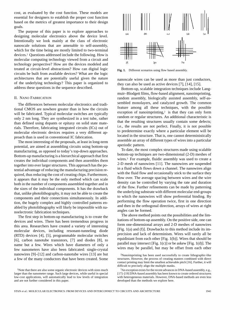
Fig. 1. Different scenarios using flow based assembly.
nanoscale wires can be used as more than just conductors,they can also be used as active devices [7], [14], [15].
Bottom-up, scalable integration techniques include Lang-muir–Blodgett films, flow-based alignment, nanoimprinting,random assembly, biologically assisted assembly, self-as-sembled monolayers, and catalyzed growth. The commonfeature among all these techniques, with the possibleexception of nanoimprinting,2 is that they can only formrandom or regular structures. An additional characteristic isthat the resulting structures usually contain some defects;i.e., the results are not perfect. Finally, it is not possibleto predetermine exactly where a particular element will belocated in the structure. That is, one cannot deterministicallyassemble an array of different types of wires into a particularaperiodic pattern.
To date, the most complex structures made using scalablebottom-up techniques are two-dimensional (2-D) meshes ofwires.3 For example, fluidic assembly was used to create a2-D mesh of nanowires [11]. The nanowires are suspendedin a fluid which flows down a channel. The nanowires alignwith the fluid flow and occasionally stick to the surface theyflow over. The average spacing between wires and the wiredensity can be controlled by varying the rate and durationof the flow. Further refinements can be made by patterningthe underlying substrate with different molecular end-groupsto which the nanowires will show preferential binding. Byperforming the flow operation twice, first in one directionand then in the orthogonal direction, arrays of wires at rightangles can be formed.
The above method points out the possibilities and the lim-itations of bottom-up assembly. On the positive side, one canform one-dimensional arrays and 2-D meshes of nanowires[Fig. 1(a) and (f)]. Drawbacks to this method include its im-precision and lack of determinism. Wires will rarely all beequidistant from each other [Fig. 1(b)]. Wires that should beparallel may intersect [Fig. 1(c)] or be askew [Fig. 1(d)]. Thewires may be parallel, but may be offset from each other
2Nanoimprinting has been used successfully to create lithographic-likestructures. However, the process of creating masters combined with directcontact printing may limit the smallest achievable pitch [16]. Further, it willdifficult to precisely align the multiple masks.
3An exception exists for the recent advances in DNA-based assembly, e.g.,[17]–[19] DNA-based assembly has been known to create ordered structureswith heterogeneous materials. However, DNA-based methods are even lessdeveloped than the methods we explore here.
STAN et al.: MOLECULAR ELECTRONICS: FROM DEVICES AND INTERCONNECT TO CIRCUITS AND ARCHITECTURE 1941
[Fig. 1(e)]. Finally, it is not possible to create a predeter-mined, aperiodic pattern of different types of wires. The re-sulting arrays may contain shorts [Fig. 1(c)] or open con-nections [Fig. 1(g) and Fig. 1(h)]. Finally, the technique cannever deterministically produce complex aperiodic arrange-ments of the wires.
Another approach for creating crossbars is to use nanoim-printing, in which a master is made using techniques suchas electron-beam lithography. The result is a stamp that hasridges and trenches. When the master is pressed onto a targetsurface, usually coated with a soft material, such as plasticdeformation magnetic assembly (PDMA), the result is thatthe pattern on the master is transferred to the target. The re-sulting surface can be then be functionalized. For example,the trenches on the target can be filled with metal to createwires. Researchers at Hewlett-Packard (HP) have recentlyused this technique to make a 64-b molecular memory. Theyuse the master to create parallel wires in one direction, fillthe trenches with wires, coat the surface with a molecularswitch, and then rotate the master by 90to make a secondimprint. The result is a crossbar made with 40-nm-wide wiresat a pitch of slightly more than 100 nm. At each junctionbetween two wires, there are approximately 1000 moleculeswhich can serve as a bit of memory.
A. Implications on Circuits and Architectures
The use of self-assembly as the dominant means of circuitassembly imposes the most severe limitations on nanoscalearchitectures: it will be difficult to create either precise align-ment between components or deterministic aperiodic struc-tures. Chemical self-assembly, as a stochastic process, willnot always produce precise alignment of structures, and ma-nipulation of single nanoscale structures to construct large-scale ordered circuits, as currently built in silicon, is imprac-tical. Furthermore, the methods used to assemble nanoscalecomponents are most effective at creating random, or, at best,crystal-like structures. These two facts have significant im-plications on the kinds of circuits and structures that can berealized at the time of fabrication.
The structural implications of bottom-up assembly are asfollows.
1) Two-terminal devices are preferred. The easiest de-vices to incorporate into a circuit will be devices withtwo terminals, e.g., diodes, configurable switches, andmolecular negative-differential resistance (NDR) de-vices. It is much easier to bring two terminals into pre-cise proximity than three.
2) Connections by overlapping wires. Lack of precisealignment means that end-to-end connections betweengroups of nanoscale wires will be nearly impossibleto achieve. A scheme where all connections betweennanoscale wires occur only when the wires are or-thogonal and overlap, reduces the need to preciselyalign the wires.
3) Meshes are a common basic unit. Since practical fore-seeable nanocomputer design will have to rely on theplacement of active components at wire intersections,
many concepts rely on using a crossbar array or meshas a basic repeated unit. More complicated structureswill have to be created either by combining meshes to-gether or cutting the wires in a mesh to break it up intosubarrays.
4) Randomness has to be accepted. Random assembly isa matter of fact. There are different ways of viewingrandomness. One is to view it as a defect pattern thathas to be coped with, e.g., a crossbar array with anumber of shorts and opens in it. Another is to use el-ements to program around defects or to create higherlevels of order—for example, using programmable de-vices as fuses or antifuses.
5) Nanoscale to microscale connections will have to besparse. A direct implication of the size differencebetween the nanoscale and the microscale is thatconnections between the two will have to be few. Ifthere are many connections between the two worlds,the density of the nanoscale components will be dic-tated by the density of the microscale. For example,using a demultiplexor to connect microscale wires tonanoscale wires would at any particular instant allowone of nanoscale wires to be addressed usingmicroscale wires. As grows large, the nanoscalewires, not the microscale wires, dominate the device.
The architectural implications of molecular electronicsand self-assembly are as follows.
1) Fine-grained reconfigurable. The most likely as-sembly processes are best at creating crystal-likestructures, e.g., 2-D meshes. Thus, the resulting struc-tures cannot directly implement a complex, aperiodiccircuit. To create useful aperiodic circuits will requirethat the device be configured after it is manufactured.
2) Defect tolerance. The stochastic process behindmolecular self-assembly will inevitably give rise todefects in the manufactured structures. Instead ofdefect densities in the range of one part per billion(as one gets in silicon), defect densities for bottom-upassembly may be as high as a few percent. The ar-chitecture will have to be designed to include spares,which can be used in place of defective components.Another useful design criterion will be to ensure thatwhen a set of components is assembled into a largerstructure, i.e., wires into parallel wires, the individualcomponents are interchangeable. For example, in a setof parallel wires, it should not mattera priori whichworking wire is used to implement a particular circuit.Rather than attempting to eliminate all the defectscompletely with manufacturing techniques, one canalso rely on postfabrication steps that allow the chipto work in spite of its defects. A natural method ofhandling the defects, first used in the Teramac [20],is to design the device to be reconfigurable and thenexploit its reconfigurable nature. After fabrication,the device can be configured to test itself, the resultof testing being a map of the device’s defects. Thedefect map can then be used to configure the device to
1942 PROCEEDINGS OF THE IEEE, VOL. 91, NO. 11, NOVEMBER 2003
implement a particular function in a way that avoidsor incorporates the detected defects.
3) Locality. As devices and wires scale down to molec-ular dimensions, the wires become an increasinglyimportant part of the total design. This is truenot only for molecular computing, but also forend-of-the-roadmap CMOS [21]. Architectures withsignificant locality (and, thus, the ability to communi-cate most frequently over shorter wires), will have anadvantage.
III. N ANODEVICES AND MODELS
We begin our discussion of molecular electronics abstrac-tions by examining molecular device modeling. The push toscale electronics to nanometer dimensions is bringing newdevice phenomena to the forefront. Experiment and theoryshow nanoscale devices may exhibit nonclassical character-istics due to electron energy discreteness, electron tunneling,and Coulomb blockade effects. Although some of these phe-nomena may be considered parasitic in conventional devices,it is possible that nanoelectronic circuits and systems mayachieve greater performance through the utilization of suchnonclassical behavior. As discussed above, modeling the be-havior of nanoscale devices in a manner that allows com-plex circuits to be simulated in a reasonable amount of timerequires new approaches to device modeling. Furthermore,with the field of nanoelectronics being in such an infant stage,there have been many new devices proposed. The ability toquickly and easily create robust device models will aid devicedesigners and circuit designers in evaluating the applicabilityof new devices.
Many efforts are underway for developing solid-statemodels for nanoscale systems [22], [23]. However, the ma-jority of the higher level work in molecular nanoelectronicshas for the most part skipped the circuit level and focused onarchitectures [24]–[27]. Thus, modeling molecular devicesat the level of abstraction needed for circuit design requiresa jump start to fill the gap between the device level workand the architectural proposals.
The conventional method for modeling devices for use incircuit simulation, such as MOSFETs, incrementally buildson a well-established model framework. However, newly de-signed nanoscale devices do not have this legacy and needto be modeled from the ground up. Furthermore, because thenonclassical characteristics observed in these devices and theunderlying physics are not yet completely understood, it isdifficult to develop compact physics-based models for all thedevices that require evaluation at the circuit level.
We classify underlying modeling approaches asphysics-based, component-based, and empirical models.Previous work on nonclassical device models for SPICEsimulation includes models for RTDs [22], [28] andsingle-electron transistors (SETs) [23]. The RTD modelsmentioned above exhibit the two extremes for modeling andimplementation approaches. Bhattacharya and Mazumder[22] have developed a physics-based RTD using the com-pact RTD equations presented in [29]. This compiled modelwas added to the open-source Berkeley SPICE simulator.The advantages of this model [22] include fast and robust
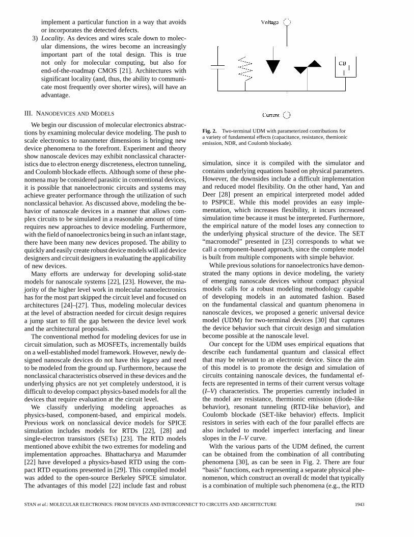
Fig. 2. Two-terminal UDM with parameterized contributions fora variety of fundamental effects (capacitance, resistance, themionicemission, NDR, and Coulomb blockade).
simulation, since it is compiled with the simulator andcontains underlying equations based on physical parameters.However, the downsides include a difficult implementationand reduced model flexibility. On the other hand, Yan andDeer [28] present an empirical interpreted model addedto PSPICE. While this model provides an easy imple-mentation, which increases flexibility, it incurs increasedsimulation time because it must be interpreted. Furthermore,the empirical nature of the model loses any connection tothe underlying physical structure of the device. The SET“macromodel” presented in [23] corresponds to what wecall a component-based approach, since the complete modelis built from multiple components with simple behavior.
While previous solutions for nanoelectronics have demon-strated the many options in device modeling, the varietyof emerging nanoscale devices without compact physicalmodels calls for a robust modeling methodology capableof developing models in an automated fashion. Basedon the fundamental classical and quantum phenomena innanoscale devices, we proposed a generic universal devicemodel (UDM) for two-terminal devices [30] that capturesthe device behavior such that circuit design and simulationbecome possible at the nanoscale level.
Our concept for the UDM uses empirical equations thatdescribe each fundamental quantum and classical effectthat may be relevant to an electronic device. Since the aimof this model is to promote the design and simulation ofcircuits containing nanoscale devices, the fundamental ef-fects are represented in terms of their current versus voltage(I–V) characteristics. The properties currently included inthe model are resistance, thermionic emission (diode-likebehavior), resonant tunneling (RTD-like behavior), andCoulomb blockade (SET-like behavior) effects. Implicitresistors in series with each of the four parallel effects arealso included to model imperfect interfacing and linearslopes in theI–V curve.
With the various parts of the UDM defined, the currentcan be obtained from the combination of all contributingphenomena [30], as can be seen in Fig. 2. There are four“basis” functions, each representing a separate physical phe-nomenon, which construct an overall dc model that typicallyis a combination of multiple such phenomena (e.g., the RTD
STAN et al.: MOLECULAR ELECTRONICS: FROM DEVICES AND INTERCONNECT TO CIRCUITS AND ARCHITECTURE 1943
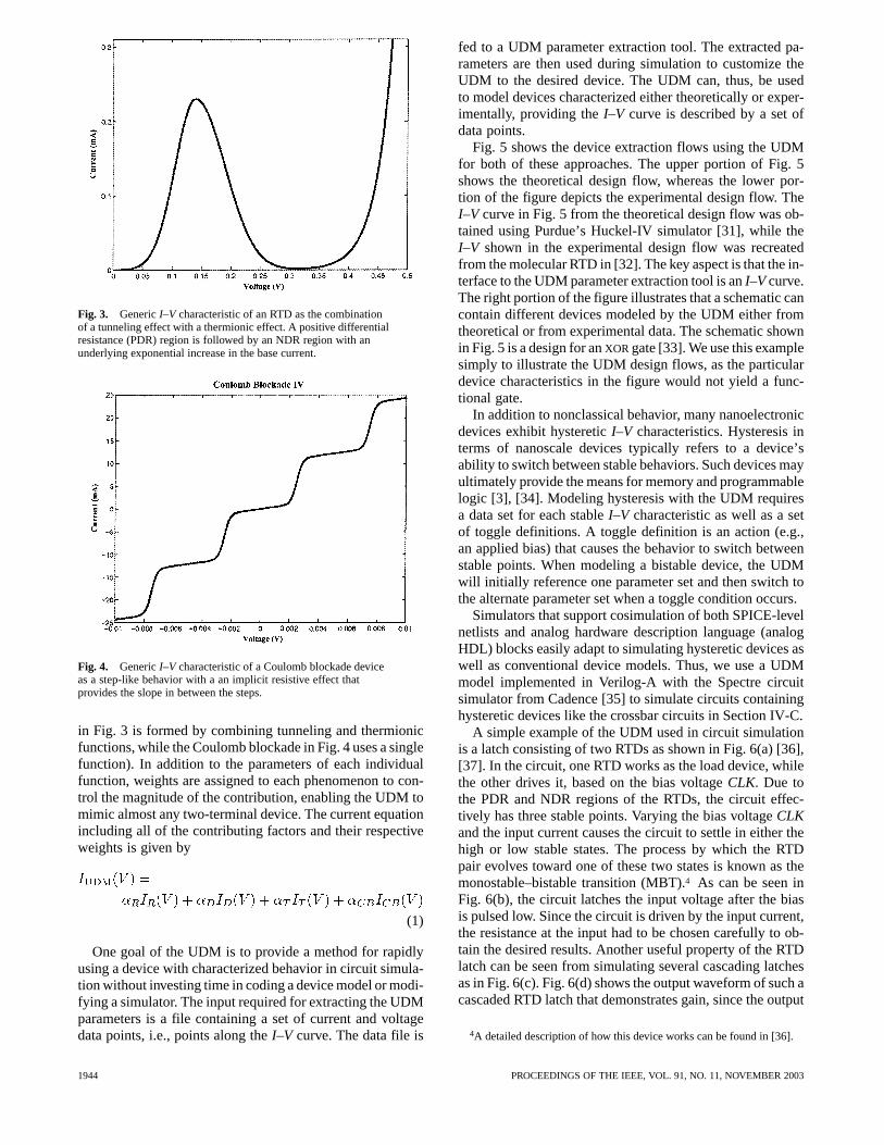
Fig. 3. GenericI–V characteristic of an RTD as the combinationof a tunneling effect with a thermionic effect. A positive differentialresistance (PDR) region is followed by an NDR region with anunderlying exponential increase in the base current.
Fig. 4. GenericI–V characteristic of a Coulomb blockade deviceas a step-like behavior with a an implicit resistive effect thatprovides the slope in between the steps.
in Fig. 3 is formed by combining tunneling and thermionicfunctions, while the Coulomb blockade in Fig. 4 uses a singlefunction). In addition to the parameters of each individualfunction, weights are assigned to each phenomenon to con-trol the magnitude of the contribution, enabling the UDM tomimic almost any two-terminal device. The current equationincluding all of the contributing factors and their respectiveweights is given by
(1)
One goal of the UDM is to provide a method for rapidlyusing a device with characterized behavior in circuit simula-tion without investing time in coding a device model or modi-fying a simulator. The input required for extracting the UDMparameters is a file containing a set of current and voltagedata points, i.e., points along theI–V curve. The data file is
fed to a UDM parameter extraction tool. The extracted pa-rameters are then used during simulation to customize theUDM to the desired device. The UDM can, thus, be usedto model devices characterized either theoretically or exper-imentally, providing theI–V curve is described by a set ofdata points.
Fig. 5 shows the device extraction flows using the UDMfor both of these approaches. The upper portion of Fig. 5shows the theoretical design flow, whereas the lower por-tion of the figure depicts the experimental design flow. TheI–V curve in Fig. 5 from the theoretical design flow was ob-tained using Purdue’s Huckel-IV simulator [31], while theI–V shown in the experimental design flow was recreatedfrom the molecular RTD in [32]. The key aspect is that the in-terface to the UDM parameter extraction tool is anI–Vcurve.The right portion of the figure illustrates that a schematic cancontain different devices modeled by the UDM either fromtheoretical or from experimental data. The schematic shownin Fig. 5 is a design for anXOR gate [33]. We use this examplesimply to illustrate the UDM design flows, as the particulardevice characteristics in the figure would not yield a func-tional gate.
In addition to nonclassical behavior, many nanoelectronicdevices exhibit hystereticI–V characteristics. Hysteresis interms of nanoscale devices typically refers to a device’sability to switch between stable behaviors. Such devices mayultimately provide the means for memory and programmablelogic [3], [34]. Modeling hysteresis with the UDM requiresa data set for each stableI–V characteristic as well as a setof toggle definitions. A toggle definition is an action (e.g.,an applied bias) that causes the behavior to switch betweenstable points. When modeling a bistable device, the UDMwill initially reference one parameter set and then switch tothe alternate parameter set when a toggle condition occurs.
Simulators that support cosimulation of both SPICE-levelnetlists and analog hardware description language (analogHDL) blocks easily adapt to simulating hysteretic devices aswell as conventional device models. Thus, we use a UDMmodel implemented in Verilog-A with the Spectre circuitsimulator from Cadence [35] to simulate circuits containinghysteretic devices like the crossbar circuits in Section IV-C.
A simple example of the UDM used in circuit simulationis a latch consisting of two RTDs as shown in Fig. 6(a) [36],[37]. In the circuit, one RTD works as the load device, whilethe other drives it, based on the bias voltageCLK. Due tothe PDR and NDR regions of the RTDs, the circuit effec-tively has three stable points. Varying the bias voltageCLKand the input current causes the circuit to settle in either thehigh or low stable states. The process by which the RTDpair evolves toward one of these two states is known as themonostable–bistable transition (MBT).4 As can be seen inFig. 6(b), the circuit latches the input voltage after the biasis pulsed low. Since the circuit is driven by the input current,the resistance at the input had to be chosen carefully to ob-tain the desired results. Another useful property of the RTDlatch can be seen from simulating several cascading latchesas in Fig. 6(c). Fig. 6(d) shows the output waveform of such acascaded RTD latch that demonstrates gain, since the output
4A detailed description of how this device works can be found in [36].
1944 PROCEEDINGS OF THE IEEE, VOL. 91, NO. 11, NOVEMBER 2003
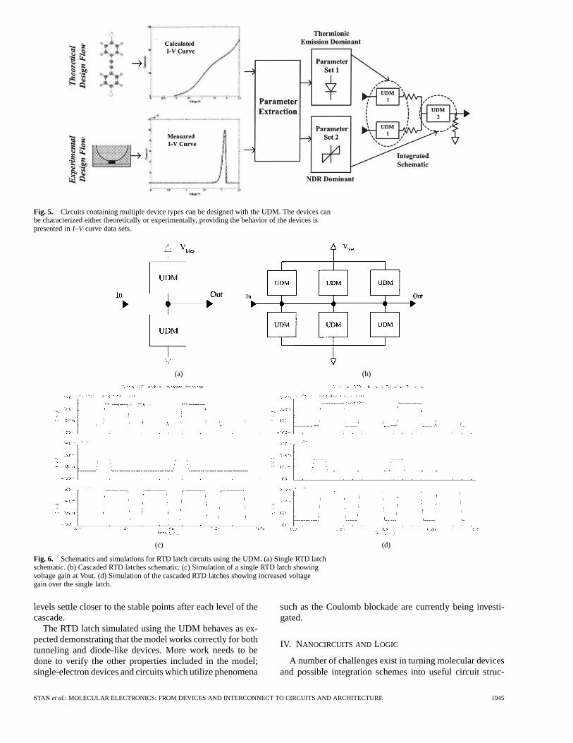
Fig. 5. Circuits containing multiple device types can be designed with the UDM. The devices canbe characterized either theoretically or experimentally, providing the behavior of the devices ispresented inI–V curve data sets.
(a) (b)
(c) (d)
Fig. 6. Schematics and simulations for RTD latch circuits using the UDM. (a) Single RTD latchschematic. (b) Cascaded RTD latches schematic. (c) Simulation of a single RTD latch showingvoltage gain at Vout. (d) Simulation of the cascaded RTD latches showing increased voltagegain over the single latch.
levels settle closer to the stable points after each level of thecascade.
The RTD latch simulated using the UDM behaves as ex-pected demonstrating that the model works correctly for bothtunneling and diode-like devices. More work needs to bedone to verify the other properties included in the model;single-electron devices and circuits which utilize phenomena
such as the Coulomb blockade are currently being investi-gated.
IV. NANOCIRCUITS AND LOGIC
A number of challenges exist in turning molecular devicesand possible integration schemes into useful circuit struc-
STAN et al.: MOLECULAR ELECTRONICS: FROM DEVICES AND INTERCONNECT TO CIRCUITS AND ARCHITECTURE 1945
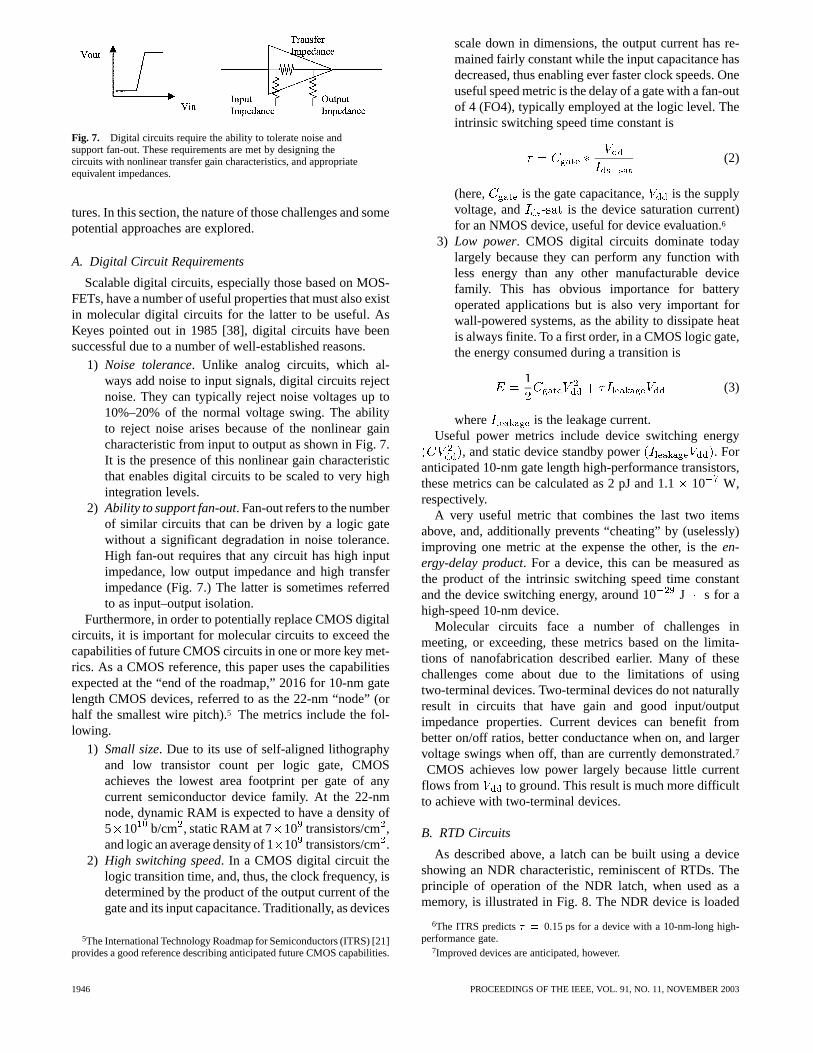
Fig. 7. Digital circuits require the ability to tolerate noise andsupport fan-out. These requirements are met by designing thecircuits with nonlinear transfer gain characteristics, and appropriateequivalent impedances.
tures. In this section, the nature of those challenges and somepotential approaches are explored.
A. Digital Circuit Requirements
Scalable digital circuits, especially those based on MOS-FETs, have a number of useful properties that must also existin molecular digital circuits for the latter to be useful. AsKeyes pointed out in 1985 [38], digital circuits have beensuccessful due to a number of well-established reasons.
1) Noise tolerance. Unlike analog circuits, which al-ways add noise to input signals, digital circuits rejectnoise. They can typically reject noise voltages up to10%–20% of the normal voltage swing. The abilityto reject noise arises because of the nonlinear gaincharacteristic from input to output as shown in Fig. 7.It is the presence of this nonlinear gain characteristicthat enables digital circuits to be scaled to very highintegration levels.
2) Ability to support fan-out. Fan-out refers to the numberof similar circuits that can be driven by a logic gatewithout a significant degradation in noise tolerance.High fan-out requires that any circuit has high inputimpedance, low output impedance and high transferimpedance (Fig. 7.) The latter is sometimes referredto as input–output isolation.
Furthermore, in order to potentially replace CMOS digitalcircuits, it is important for molecular circuits to exceed thecapabilities of future CMOS circuits in one or more key met-rics. As a CMOS reference, this paper uses the capabilitiesexpected at the “end of the roadmap,” 2016 for 10-nm gatelength CMOS devices, referred to as the 22-nm “node” (orhalf the smallest wire pitch).5 The metrics include the fol-lowing.
1) Small size. Due to its use of self-aligned lithographyand low transistor count per logic gate, CMOSachieves the lowest area footprint per gate of anycurrent semiconductor device family. At the 22-nmnode, dynamic RAM is expected to have a density of5 10 b/cm , static RAM at 7 10 transistors/cm,and logic an average density of 110 transistors/cm.
2) High switching speed. In a CMOS digital circuit thelogic transition time, and, thus, the clock frequency, isdetermined by the product of the output current of thegate and its input capacitance. Traditionally, as devices
5The International Technology Roadmap for Semiconductors (ITRS) [21]provides a good reference describing anticipated future CMOS capabilities.
scale down in dimensions, the output current has re-mained fairly constant while the input capacitance hasdecreased, thus enabling ever faster clock speeds. Oneuseful speed metric is the delay of a gate with a fan-outof 4 (FO4), typically employed at the logic level. Theintrinsic switching speed time constant is
(2)
(here, is the gate capacitance, is the supplyvoltage, and - is the device saturation current)for an NMOS device, useful for device evaluation.6
3) Low power. CMOS digital circuits dominate todaylargely because they can perform any function withless energy than any other manufacturable devicefamily. This has obvious importance for batteryoperated applications but is also very important forwall-powered systems, as the ability to dissipate heatis always finite. To a first order, in a CMOS logic gate,the energy consumed during a transition is
(3)
where is the leakage current.Useful power metrics include device switching energy
, and static device standby power . Foranticipated 10-nm gate length high-performance transistors,these metrics can be calculated as 2 pJ and 1.110 W,respectively.
A very useful metric that combines the last two itemsabove, and, additionally prevents “cheating” by (uselessly)improving one metric at the expense the other, is theen-ergy-delay product. For a device, this can be measured asthe product of the intrinsic switching speed time constantand the device switching energy, around 10J s for ahigh-speed 10-nm device.
Molecular circuits face a number of challenges inmeeting, or exceeding, these metrics based on the limita-tions of nanofabrication described earlier. Many of thesechallenges come about due to the limitations of usingtwo-terminal devices. Two-terminal devices do not naturallyresult in circuits that have gain and good input/outputimpedance properties. Current devices can benefit frombetter on/off ratios, better conductance when on, and largervoltage swings when off, than are currently demonstrated.7
CMOS achieves low power largely because little currentflows from to ground. This result is much more difficultto achieve with two-terminal devices.
B. RTD Circuits
As described above, a latch can be built using a deviceshowing an NDR characteristic, reminiscent of RTDs. Theprinciple of operation of the NDR latch, when used as amemory, is illustrated in Fig. 8. The NDR device is loaded
6The ITRS predicts� = 0.15 ps for a device with a 10-nm-long high-performance gate.
7Improved devices are anticipated, however.
1946 PROCEEDINGS OF THE IEEE, VOL. 91, NO. 11, NOVEMBER 2003
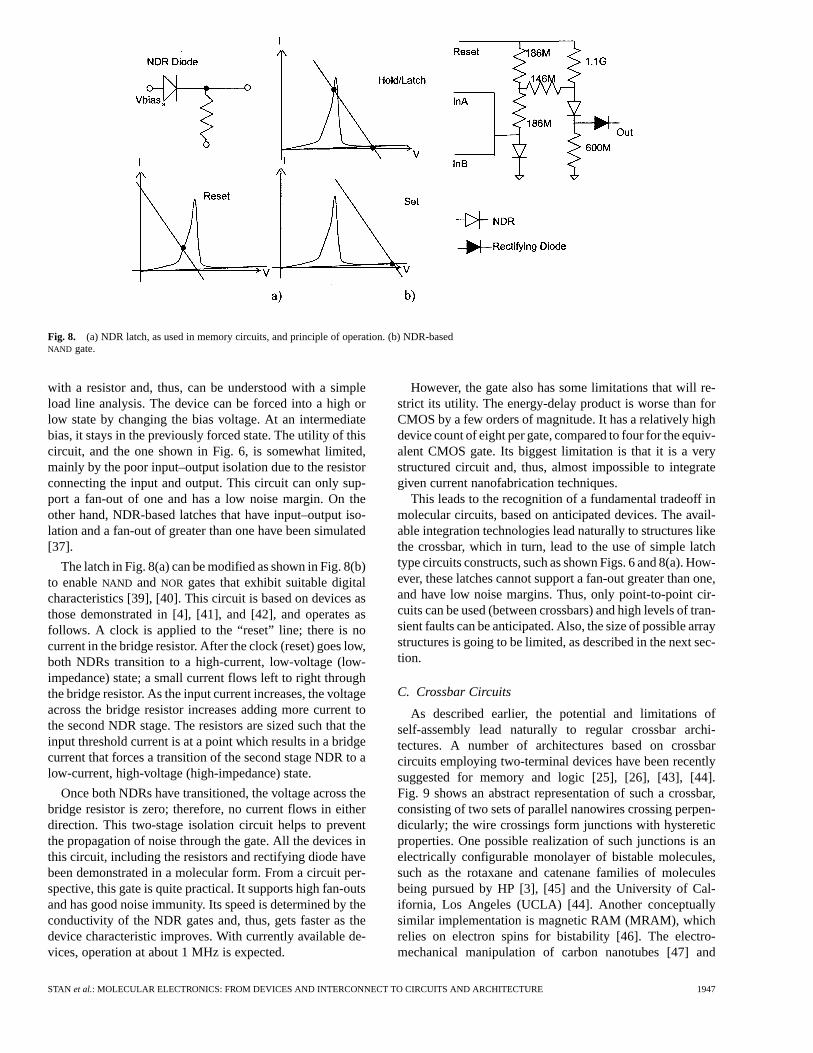
Fig. 8. (a) NDR latch, as used in memory circuits, and principle of operation. (b) NDR-basedNAND gate.
with a resistor and, thus, can be understood with a simpleload line analysis. The device can be forced into a high orlow state by changing the bias voltage. At an intermediatebias, it stays in the previously forced state. The utility of thiscircuit, and the one shown in Fig. 6, is somewhat limited,mainly by the poor input–output isolation due to the resistorconnecting the input and output. This circuit can only sup-port a fan-out of one and has a low noise margin. On theother hand, NDR-based latches that have input–output iso-lation and a fan-out of greater than one have been simulated[37].
The latch in Fig. 8(a) can be modified as shown in Fig. 8(b)to enableNAND and NOR gates that exhibit suitable digitalcharacteristics [39], [40]. This circuit is based on devices asthose demonstrated in [4], [41], and [42], and operates asfollows. A clock is applied to the “reset” line; there is nocurrent in the bridge resistor. After the clock (reset) goes low,both NDRs transition to a high-current, low-voltage (low-impedance) state; a small current flows left to right throughthe bridge resistor. As the input current increases, the voltageacross the bridge resistor increases adding more current tothe second NDR stage. The resistors are sized such that theinput threshold current is at a point which results in a bridgecurrent that forces a transition of the second stage NDR to alow-current, high-voltage (high-impedance) state.
Once both NDRs have transitioned, the voltage across thebridge resistor is zero; therefore, no current flows in eitherdirection. This two-stage isolation circuit helps to preventthe propagation of noise through the gate. All the devices inthis circuit, including the resistors and rectifying diode havebeen demonstrated in a molecular form. From a circuit per-spective, this gate is quite practical. It supports high fan-outsand has good noise immunity. Its speed is determined by theconductivity of the NDR gates and, thus, gets faster as thedevice characteristic improves. With currently available de-vices, operation at about 1 MHz is expected.
However, the gate also has some limitations that will re-strict its utility. The energy-delay product is worse than forCMOS by a few orders of magnitude. It has a relatively highdevice count of eight per gate, compared to four for the equiv-alent CMOS gate. Its biggest limitation is that it is a verystructured circuit and, thus, almost impossible to integrategiven current nanofabrication techniques.
This leads to the recognition of a fundamental tradeoff inmolecular circuits, based on anticipated devices. The avail-able integration technologies lead naturally to structures likethe crossbar, which in turn, lead to the use of simple latchtype circuits constructs, such as shown Figs. 6 and 8(a). How-ever, these latches cannot support a fan-out greater than one,and have low noise margins. Thus, only point-to-point cir-cuits can be used (between crossbars) and high levels of tran-sient faults can be anticipated. Also, the size of possible arraystructures is going to be limited, as described in the next sec-tion.
C. Crossbar Circuits
As described earlier, the potential and limitations ofself-assembly lead naturally to regular crossbar archi-tectures. A number of architectures based on crossbarcircuits employing two-terminal devices have been recentlysuggested for memory and logic [25], [26], [43], [44].Fig. 9 shows an abstract representation of such a crossbar,consisting of two sets of parallel nanowires crossing perpen-dicularly; the wire crossings form junctions with hystereticproperties. One possible realization of such junctions is anelectrically configurable monolayer of bistable molecules,such as the rotaxane and catenane families of moleculesbeing pursued by HP [3], [45] and the University of Cal-ifornia, Los Angeles (UCLA) [44]. Another conceptuallysimilar implementation is magnetic RAM (MRAM), whichrelies on electron spins for bistability [46]. The electro-mechanical manipulation of carbon nanotubes [47] and
STAN et al.: MOLECULAR ELECTRONICS: FROM DEVICES AND INTERCONNECT TO CIRCUITS AND ARCHITECTURE 1947
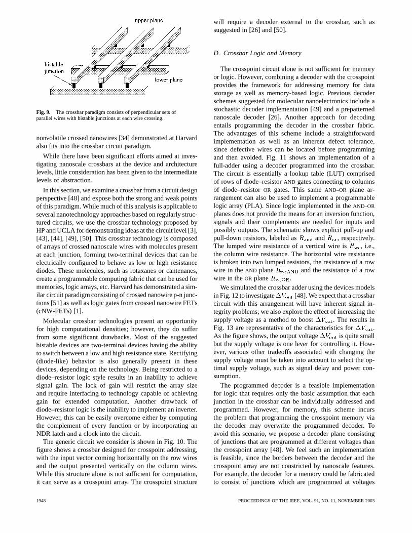
Fig. 9. The crossbar paradigm consists of perpendicular sets ofparallel wires with bistable junctions at each wire crossing.
nonvolatile crossed nanowires [34] demonstrated at Harvardalso fits into the crossbar circuit paradigm.
While there have been significant efforts aimed at inves-tigating nanoscale crossbars at the device and architecturelevels, little consideration has been given to the intermediatelevels of abstraction.
In this section, we examine a crossbar from a circuit designperspective [48] and expose both the strong and weak pointsof this paradigm. While much of this analysis is applicable toseveral nanotechnology approaches based on regularly struc-tured circuits, we use the crossbar technology proposed byHP and UCLA for demonstrating ideas at the circuit level [3],[43], [44], [49], [50]. This crossbar technology is composedof arrays of crossed nanoscale wires with molecules presentat each junction, forming two-terminal devices that can beelectrically configured to behave as low or high resistancediodes. These molecules, such as rotaxanes or cantenanes,create a programmable computing fabric that can be used formemories, logic arrays, etc. Harvard has demonstrated a sim-ilar circuit paradigm consisting of crossed nanowire p-n junc-tions [51] as well as logic gates from crossed nanowire FETs(cNW-FETs) [1].
Molecular crossbar technologies present an opportunityfor high computational densities; however, they do sufferfrom some significant drawbacks. Most of the suggestedbistable devices are two-terminal devices having the abilityto switch between a low and high resistance state. Rectifying(diode-like) behavior is also generally present in thesedevices, depending on the technology. Being restricted to adiode–resistor logic style results in an inability to achievesignal gain. The lack of gain will restrict the array sizeand require interfacing to technology capable of achievinggain for extended computation. Another drawback ofdiode–resistor logic is the inability to implement an inverter.However, this can be easily overcome either by computingthe complement of every function or by incorporating anNDR latch and a clock into the circuit.
The generic circuit we consider is shown in Fig. 10. Thefigure shows a crossbar designed for crosspoint addressing,with the input vector coming horizontally on the row wiresand the output presented vertically on the column wires.While this structure alone is not sufficient for computation,it can serve as a crosspoint array. The crosspoint structure
will require a decoder external to the crossbar, such assuggested in [26] and [50].
D. Crossbar Logic and Memory
The crosspoint circuit alone is not sufficient for memoryor logic. However, combining a decoder with the crosspointprovides the framework for addressing memory for datastorage as well as memory-based logic. Previous decoderschemes suggested for molecular nanoelectronics include astochastic decoder implementation [49] and a prepatternednanoscale decoder [26]. Another approach for decodingentails programming the decoder in the crossbar fabric.The advantages of this scheme include a straightforwardimplementation as well as an inherent defect tolerance,since defective wires can be located before programmingand then avoided. Fig. 11 shows an implementation of afull-adder using a decoder programmed into the crossbar.The circuit is essentially a lookup table (LUT) comprisedof rows of diode–resistorAND gates connecting to columnsof diode–resistorOR gates. This sameAND–OR plane ar-rangement can also be used to implement a programmablelogic array (PLA). Since logic implemented in theAND–OR
planes does not provide the means for an inversion function,signals and their complements are needed for inputs andpossibly outputs. The schematic shows explicit pull-up andpull-down resistors, labeled as and , respectively.The lumped wire resistance of a vertical wire is , i.e.,the column wire resistance. The horizontal wire resistanceis broken into two lumped resistors, the resistance of a rowwire in theAND plane and the resistance of a rowwire in theOR plane .
We simulated the crossbar adder using the devices modelsin Fig. 12 to investigate [48]. We expect that a crossbarcircuit with this arrangement will have inherent signal in-tegrity problems; we also explore the effect of increasing thesupply voltage as a method to boost . The results inFig. 13 are representative of the characteristics for .As the figure shows, the output voltage is quite smallbut the supply voltage is one lever for controlling it. How-ever, various other tradeoffs associated with changing thesupply voltage must be taken into account to select the op-timal supply voltage, such as signal delay and power con-sumption.
The programmed decoder is a feasible implementationfor logic that requires only the basic assumption that eachjunction in the crossbar can be individually addressed andprogrammed. However, for memory, this scheme incursthe problem that programming the crosspoint memory viathe decoder may overwrite the programmed decoder. Toavoid this scenario, we propose a decoder plane consistingof junctions that are programmed at different voltages thanthe crosspoint array [48]. We feel such an implementationis feasible, since the borders between the decoder and thecrosspoint array are not constricted by nanoscale features.For example, the decoder for a memory could be fabricatedto consist of junctions which are programmed at voltages
1948 PROCEEDINGS OF THE IEEE, VOL. 91, NO. 11, NOVEMBER 2003
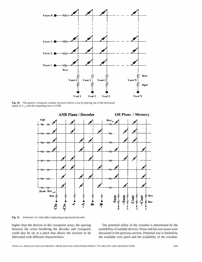
Fig. 10. The generic crosspoint crossbar structure selects a row by placing one of the horizontalinputs toV and the remaining rows to GND.
Fig. 11. Schematic of a full-adder employing programmed decoder.
higher than the devices in the crosspoint array; the spacingbetween the wires bordering the decoder and crosspointcould also be set at a pitch that allows the sections to befabricated with different characteristics.
The potential utility of the crossbar is determined by theavailability of suitable devices. Noise and fan-out issues werediscussed in the previous section. Potential size is limited bythe available wire pitch and the scalability of the crossbar.
STAN et al.: MOLECULAR ELECTRONICS: FROM DEVICES AND INTERCONNECT TO CIRCUITS AND ARCHITECTURE 1949
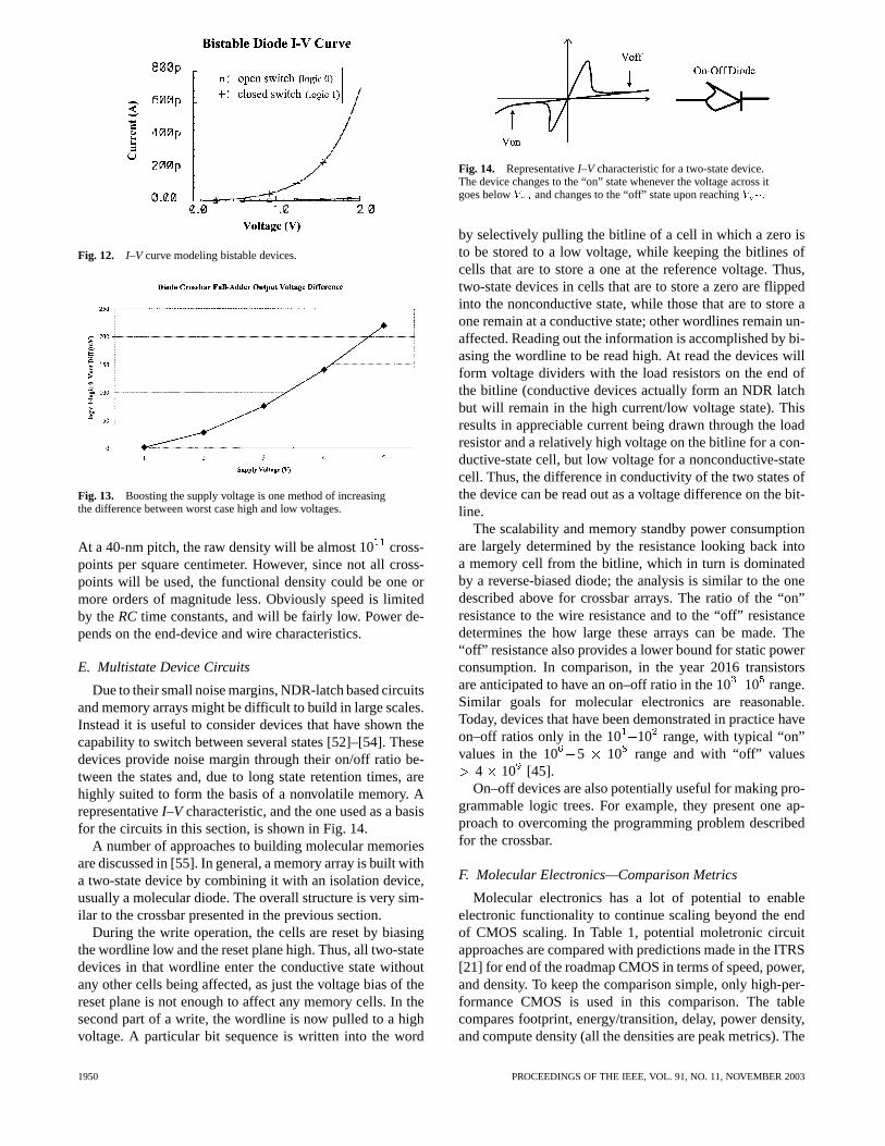
Fig. 12. I–V curve modeling bistable devices.
Fig. 13. Boosting the supply voltage is one method of increasingthe difference between worst case high and low voltages.
At a 40-nm pitch, the raw density will be almost 10cross-points per square centimeter. However, since not all cross-points will be used, the functional density could be one ormore orders of magnitude less. Obviously speed is limitedby theRC time constants, and will be fairly low. Power de-pends on the end-device and wire characteristics.
E. Multistate Device Circuits
Due to their small noise margins, NDR-latch based circuitsand memory arrays might be difficult to build in large scales.Instead it is useful to consider devices that have shown thecapability to switch between several states [52]–[54]. Thesedevices provide noise margin through their on/off ratio be-tween the states and, due to long state retention times, arehighly suited to form the basis of a nonvolatile memory. ArepresentativeI–V characteristic, and the one used as a basisfor the circuits in this section, is shown in Fig. 14.
A number of approaches to building molecular memoriesare discussed in [55]. In general, a memory array is built witha two-state device by combining it with an isolation device,usually a molecular diode. The overall structure is very sim-ilar to the crossbar presented in the previous section.
During the write operation, the cells are reset by biasingthe wordline low and the reset plane high. Thus, all two-statedevices in that wordline enter the conductive state withoutany other cells being affected, as just the voltage bias of thereset plane is not enough to affect any memory cells. In thesecond part of a write, the wordline is now pulled to a highvoltage. A particular bit sequence is written into the word
Fig. 14. RepresentativeI–V characteristic for a two-state device.The device changes to the “on” state whenever the voltage across itgoes belowV and changes to the “off” state upon reachingV .
by selectively pulling the bitline of a cell in which a zero isto be stored to a low voltage, while keeping the bitlines ofcells that are to store a one at the reference voltage. Thus,two-state devices in cells that are to store a zero are flippedinto the nonconductive state, while those that are to store aone remain at a conductive state; other wordlines remain un-affected. Reading out the information is accomplished by bi-asing the wordline to be read high. At read the devices willform voltage dividers with the load resistors on the end ofthe bitline (conductive devices actually form an NDR latchbut will remain in the high current/low voltage state). Thisresults in appreciable current being drawn through the loadresistor and a relatively high voltage on the bitline for a con-ductive-state cell, but low voltage for a nonconductive-statecell. Thus, the difference in conductivity of the two states ofthe device can be read out as a voltage difference on the bit-line.
The scalability and memory standby power consumptionare largely determined by the resistance looking back intoa memory cell from the bitline, which in turn is dominatedby a reverse-biased diode; the analysis is similar to the onedescribed above for crossbar arrays. The ratio of the “on”resistance to the wire resistance and to the “off” resistancedetermines the how large these arrays can be made. The“off” resistance also provides a lower bound for static powerconsumption. In comparison, in the year 2016 transistorsare anticipated to have an on–off ratio in the 1010 range.Similar goals for molecular electronics are reasonable.Today, devices that have been demonstrated in practice haveon–off ratios only in the 10 10 range, with typical “on”values in the 10 5 10 range and with “off” values
4 10 [45].On–off devices are also potentially useful for making pro-
grammable logic trees. For example, they present one ap-proach to overcoming the programming problem describedfor the crossbar.
F. Molecular Electronics—Comparison Metrics
Molecular electronics has a lot of potential to enableelectronic functionality to continue scaling beyond the endof CMOS scaling. In Table 1, potential moletronic circuitapproaches are compared with predictions made in the ITRS[21] for end of the roadmap CMOS in terms of speed, power,and density. To keep the comparison simple, only high-per-formance CMOS is used in this comparison. The tablecompares footprint, energy/transition, delay, power density,and compute density (all the densities are peak metrics). The
1950 PROCEEDINGS OF THE IEEE, VOL. 91, NO. 11, NOVEMBER 2003
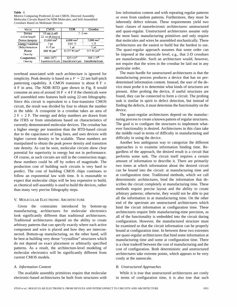
Table 1Metrics Comparing Predicted 22-nm CMOS, Directed AssemblyMolecular Circuits Based On NDR Molecules, and Self-AssembledCrossbars Based on Multistate Devices
overhead associated with each architecture is ignored forsimplicity. Peak density is based on a 22 nm half-pitchpatterning capability. A CMOS transistor is about 8 F4 F in area. The NDR–RTD gate shown in Fig. 8 wouldconsume an area of around 16 F4 F if the chemicals wereself assembled onto features built using 22-nm lithography.Since this circuit is equivalent to a four-transistor CMOScircuit, the result was divided by four to obtain the numberin the table. A crosspoint in a crossbar takes an area of2 F 2 F. The energy and delay numbers are drawn fromthe ITRS or from simulations based on characteristics ofcurrently demonstrated molecular devices. The crossbar hasa higher energy per transition than the RTD-based circuitdue to the capacitance of long lines, and uses devices withhigher current density to be scalable. These numbers aremanipulated to obtain the peak power density and transitionrate density. As can be seen, molecular circuits show clearpotential for superiority in energy but not in performance.Of course, as such circuits are still in the construction stage;these numbers could be off by orders of magnitude. Theproduction cost of building such circuits is very hard topredict. The cost of building CMOS chips continues tofollow an exponential law with time. It is reasonable toexpect that molecular chips will be less expensive to build,as chemical self-assembly is used to build the devices, ratherthan many very precise lithography steps.
V. MOLECULAR ELECTRONIC ARCHITECTURE
Given the constraints introduced by bottom-upmanufacturing, architectures for molecular electronicslook significantly different than traditional architectures.Traditional architectures depend on the ability to createarbitrary patterns that can specify exactly where each activecomponent and wire is placed and how they are intercon-nected. Bottom-up manufacturing, on the other hand, willbe best at building very dense “crystalline” structures whichdo not depend on exact placement or arbitrarily specifiedpatterns. As a result, the architecture-level modeling ofmolecular electronics will be significantly different fromcurrent CMOS models.
A. Information Content
The available assembly primitives require that molecularelectronic-based architectures be built from structures with
low information content and with repeating regular patternsor even from random patterns. Furthermore, they must beinherently defect tolerant. These requirements yield twobasic classes of nanoelectronic architectures: unstructuredand quasi-regular. Unstructured architectures assume onlythe most basic manufacturing primitives and only requirethat molecules and wires be assembled stochastically. Thesearchitectures are the easiest to build but the hardest to use.The quasi-regular approach assumes that some order canbe imposed at the nanoscale level, e.g., that 2-D crossbarsare manufacturable. Such an architecture would, however,not require that the wires in the crossbar be laid out in anyparticular order.
The main hurdle for unstructured architectures is that themanufacturing process produces a device that has no pre-determined information content. Instead, the user of the de-vice must probe it to determine what kinds of structures arepresent. After probing the device, if useful structures arefound, they can be connected to form a circuit. The probingtask is similar in spirit to defect detection, but instead offinding the defects, it must determine the functionality on thedevice.
The quasi-regular architectures depend on the manufac-turing process to create a known pattern of regular structures.The goal is to configure the structures to implement what-ever functionality is desired. Architectures in this class takethe middle road in terms of difficulty in manufacturing anddifficulty in using the device.
Another less ambiguous way to categorize the differentapproaches is to examine information binding time. Re-gardless of the approach, the desired result is a circuit thatperforms some task. The circuit itself requires a certainamount of information to describe it. There are primarilytwo times at which information about the desired circuitcan be bound into the circuit: at manufacturing time andat configuration time. Traditional methods, which we calldeterministic architectures, bind the information that de-scribes the circuit completely at manufacturing time. Thesemethods require precise layout and the ability to createarbitrary patterns; otherwise, they would not be able to putall the information in at manufacturing time. On the otherend of the spectrum are unstructured architectures whichbind the circuit information at configuration time. Thesearchitectures require little manufacturing-time precision, asall of the functionality is embedded into the circuit duringconfiguration. However, the manufactured structure mustbe examined so that the circuit information can be properlybound at configuration time. In between these two extremesare quasi-regular architectures that bind some information atmanufacturing time and some at configuration time. Thereis a clear tradeoff between the cost of manufacturing and thecost of configuration. Both deterministic and unstructuredarchitectures take extreme points, which appears to be verycostly at the nanoscale.
B. Unstructured Approaches
While it is true that unstructured architectures are costlyin terms of configuration time, it is also true that such
STAN et al.: MOLECULAR ELECTRONICS: FROM DEVICES AND INTERCONNECT TO CIRCUITS AND ARCHITECTURE 1951
Fig. 15. Schematic of a molecular demultiplexor based on randomassembly of gold particles to act as gates on nanoscale wires.The horizontal, wide, gray lines represent microwires, while thethin lines represent nanowires. The “dots” on the transistor gatesrepresent connections between the microscale and the nanoscale.
architectures have some clear advantages over approachesrequiring more order. A good example of how unstructuredapproaches can reduce the cost of manufacturing withoutsignificantly increasing the cost of configuration is thenondeterministic demultiplexor proposed by HP [50]. Thisdemultiplexor (demux) is formed by intersecting a parallelset of microscale wires with an orthogonal set of parallelnanoscale wires. Between the microscale wires and thenanoscale wires is a layer consisting of randomly placedgold particles. Wherever the nanoscale wires contact a goldparticle a transistor gate is formed. If the gold particle alsocontacts a microscale wire, then that microscale wire can beused to turn on that particular “transistor.” The microscalewires essentially provide an address which is used to selectone of the nanoscale wires (see Fig. 15.) A traditionaldemux using binary signals requires address wires toselect from one of outputs; however, it requires substantialprecision at the time of manufacture. The demux proposedby HP, on the other hand, requires more microscale addresslines, since the address of each nanoscale wire is formed“randomly”; furthermore, one does not know at manufac-turing time which address will select which nanoscale wire.However, the difficulty in determining the addresses is low,and with a sufficient number of micrometer-scale wires,each of the output wires can be selected ( addresslines will select each one of theoutputs with greater than50% probability). Note that the three-terminal devices inthis example can be modeled as conventional FETs with noneed for the UDM, which right now is limited to modelingtwo-terminal devices.
A more complete architecture based on the unstructuredapproach is the Nanocell [56]. The Nanocell architectureis based on the random assembly of a small grid of on–off
Fig. 16. A nanoBlock. The MLA is reconfigurable andcombines with the resistors attached toV and ground to createa reconfigurable diode–resistor logic array. Signal restoration isperformed in the molecular latches which are orthogonal to theoutput wires.
devices. The functionality of each grid is determined post-fabrication through a detection phase using external voltagepulses. Gain and input–output isolation are establishedbetween cells using NDR-latch type circuits. Preliminarycalculations show that this approach, when combined withCMOS at the 22-nm node, can achieve a functional densityequivalent to 10 devices/cm.
C. Array-Based Architectures
Array-based or crossbar-based architectures typifythe quasi-regular class of architectures. Each basic unit(crossbar) consists of wires and programmable moleculardevices. The crossbars are then connected together to forma larger mesh of configurable elements. Unlike unstructuredarchitectures, the potential functionality of array-baseddevices does not have to be discovered; however, thesearchitectures do depend on postfabrication programmingin order to create logical circuits. Furthermore, since thefabrication primitives are unlikely to yield perfect meshes,these architectures require reprogrammable components inorder to provide defect tolerance.
One such architecture is the nanoFabric [25], of whichthe basic unit of logic is a nanoBlock (see Fig. 16). EachnanoBlock is based around a molecular logic array (MLA).At each intersection of the MLA is a reconfigurable switch(e.g., a pseudo-rotaxene) in series with a diode. Diode–re-sistor logic is used to perform logical operations. To createa complete logic family, signals and their complements arebrought into each circuit and produce both the desired func-tions and their complements. Logic values are restored usingmolecular latches [37], which also provide a mechanism forlatching values and isolating outputs from one nanoBlockfrom the inputs of another nanoBlock. The nanoBlocksare grouped together into clusters and arranged so that theoutputs of a nanoBlock intersect the inputs of two other
1952 PROCEEDINGS OF THE IEEE, VOL. 91, NO. 11, NOVEMBER 2003
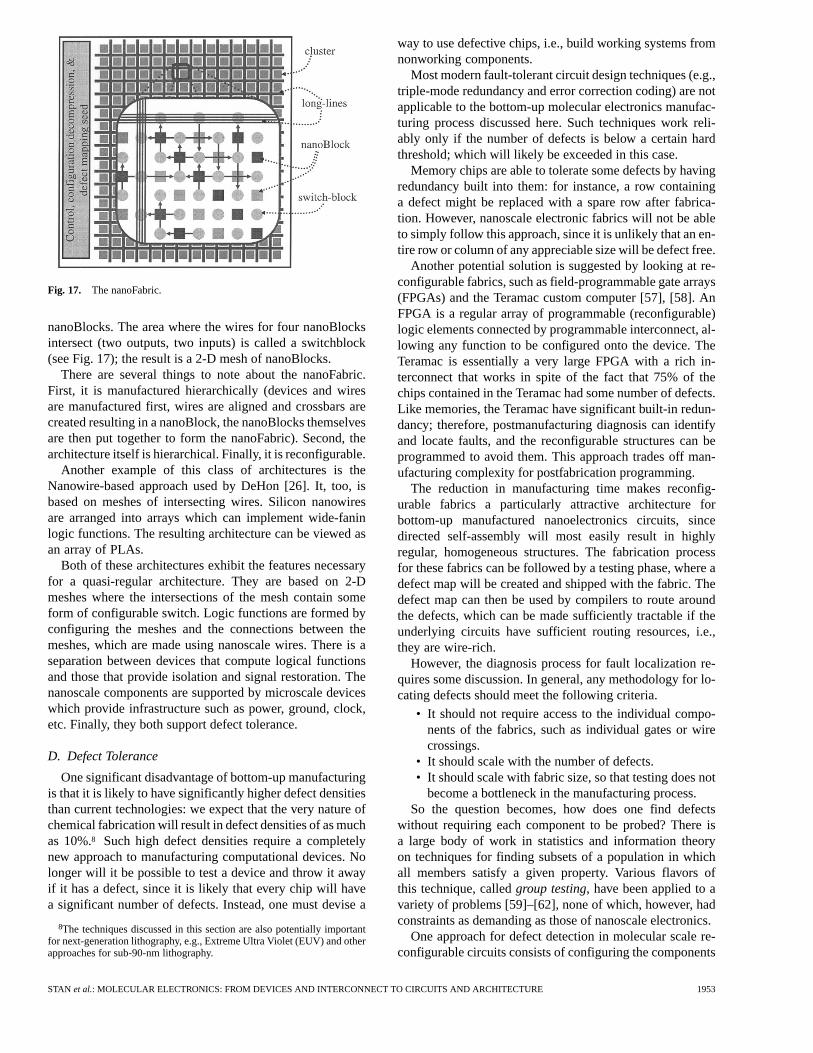
Fig. 17. The nanoFabric.
nanoBlocks. The area where the wires for four nanoBlocksintersect (two outputs, two inputs) is called a switchblock(see Fig. 17); the result is a 2-D mesh of nanoBlocks.
There are several things to note about the nanoFabric.First, it is manufactured hierarchically (devices and wiresare manufactured first, wires are aligned and crossbars arecreated resulting in a nanoBlock, the nanoBlocks themselvesare then put together to form the nanoFabric). Second, thearchitecture itself is hierarchical. Finally, it is reconfigurable.
Another example of this class of architectures is theNanowire-based approach used by DeHon [26]. It, too, isbased on meshes of intersecting wires. Silicon nanowiresare arranged into arrays which can implement wide-faninlogic functions. The resulting architecture can be viewed asan array of PLAs.
Both of these architectures exhibit the features necessaryfor a quasi-regular architecture. They are based on 2-Dmeshes where the intersections of the mesh contain someform of configurable switch. Logic functions are formed byconfiguring the meshes and the connections between themeshes, which are made using nanoscale wires. There is aseparation between devices that compute logical functionsand those that provide isolation and signal restoration. Thenanoscale components are supported by microscale deviceswhich provide infrastructure such as power, ground, clock,etc. Finally, they both support defect tolerance.
D. Defect Tolerance
One significant disadvantage of bottom-up manufacturingis that it is likely to have significantly higher defect densitiesthan current technologies: we expect that the very nature ofchemical fabrication will result in defect densities of as muchas 10%.8 Such high defect densities require a completelynew approach to manufacturing computational devices. Nolonger will it be possible to test a device and throw it awayif it has a defect, since it is likely that every chip will havea significant number of defects. Instead, one must devise a
8The techniques discussed in this section are also potentially importantfor next-generation lithography, e.g., Extreme Ultra Violet (EUV) and otherapproaches for sub-90-nm lithography.
way to use defective chips, i.e., build working systems fromnonworking components.
Most modern fault-tolerant circuit design techniques (e.g.,triple-mode redundancy and error correction coding) are notapplicable to the bottom-up molecular electronics manufac-turing process discussed here. Such techniques work reli-ably only if the number of defects is below a certain hardthreshold; which will likely be exceeded in this case.
Memory chips are able to tolerate some defects by havingredundancy built into them: for instance, a row containinga defect might be replaced with a spare row after fabrica-tion. However, nanoscale electronic fabrics will not be ableto simply follow this approach, since it is unlikely that an en-tire row or column of any appreciable size will be defect free.
Another potential solution is suggested by looking at re-configurable fabrics, such as field-programmable gate arrays(FPGAs) and the Teramac custom computer [57], [58]. AnFPGA is a regular array of programmable (reconfigurable)logic elements connected by programmable interconnect, al-lowing any function to be configured onto the device. TheTeramac is essentially a very large FPGA with a rich in-terconnect that works in spite of the fact that 75% of thechips contained in the Teramac had some number of defects.Like memories, the Teramac have significant built-in redun-dancy; therefore, postmanufacturing diagnosis can identifyand locate faults, and the reconfigurable structures can beprogrammed to avoid them. This approach trades off man-ufacturing complexity for postfabrication programming.
The reduction in manufacturing time makes reconfig-urable fabrics a particularly attractive architecture forbottom-up manufactured nanoelectronics circuits, sincedirected self-assembly will most easily result in highlyregular, homogeneous structures. The fabrication processfor these fabrics can be followed by a testing phase, where adefect map will be created and shipped with the fabric. Thedefect map can then be used by compilers to route aroundthe defects, which can be made sufficiently tractable if theunderlying circuits have sufficient routing resources, i.e.,they are wire-rich.
However, the diagnosis process for fault localization re-quires some discussion. In general, any methodology for lo-cating defects should meet the following criteria.
• It should not require access to the individual compo-nents of the fabrics, such as individual gates or wirecrossings.
• It should scale with the number of defects.• It should scale with fabric size, so that testing does not
become a bottleneck in the manufacturing process.So the question becomes, how does one find defects
without requiring each component to be probed? There isa large body of work in statistics and information theoryon techniques for finding subsets of a population in whichall members satisfy a given property. Various flavors ofthis technique, calledgroup testing, have been applied to avariety of problems [59]–[62], none of which, however, hadconstraints as demanding as those of nanoscale electronics.
One approach for defect detection in molecular scale re-configurable circuits consists of configuring the components
STAN et al.: MOLECULAR ELECTRONICS: FROM DEVICES AND INTERCONNECT TO CIRCUITS AND ARCHITECTURE 1953
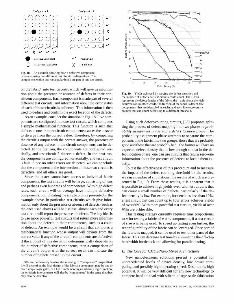
Fig. 18. An example showing how a defective componentis located using two different test circuit configurations. Thecomponents within one rectangular block are part of one test circuit.
on the fabric9 into test circuits, which will give us informa-tion about the presence or absence of defects in their con-stituent components. Each component is made part of severaldifferent test circuits, and information about the error statusof each of those circuits is collected. This information is thenused to deduce and confirm the exact location of the defects.
As an example, consider the situation in Fig. 18. Five com-ponents are configured into one test circuit, which computesa simple mathematical function. This function is such thatdefects in one or more circuit components causes the answerto diverge from the correct value. Therefore, by comparingthe circuit’s output with the correct answer, the presence orabsence of any defects in the circuit components can be de-tected. In the first run, the components are configured ver-tically, and test circuit 2 detects a defect. In the next run,the components are configured horizontally, and test circuit3 fails. Since no other errors are detected, we can concludethat the component at the intersection of these two circuits isdefective, and all others are good.
Since the tester cannot have access to individual fabriccomponents, the test circuits will be large, consisting of tensand perhaps even hundreds of components. With high defectrates, each circuit will on average have multiple defectivecomponents, complicating the simple picture presented in theexample above. In particular, test circuits which give infor-mation only about the presence or absence of defects (such asthe ones used above) will be useless: almost each and everytest circuit will report the presence of defects. The key idea isto use more powerful test circuits that return more informa-tion about the defects in their components, such as a countof defects. An example would be a circuit that computes amathematical function whose output will deviate from thecorrect value if any of the circuit’s components are defective;if the amount of this deviation deterministically depends onthe number of defective components, then a comparison ofthe circuit’s output with the correct result can indicate thenumber of defects present in the circuit.
9We are deliberately leaving the meaning of “component” unspecified.It will depend on the final design of the fabric: a component may be one ormore simple logic gates, or a LUT implementing an arbitrary logic function;the on-fabric interconnects will also be “components” in the sense that theymay also be defective.
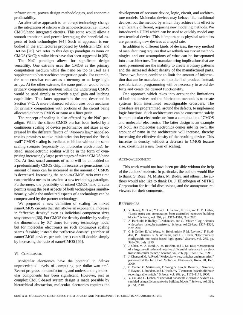
Fig. 19. Yields achieved by varying the defect densities andthe number of defects our test circuits could count. Thex axisrepresents the defect density of the fabric, they axis shows the yieldachieved (or, in other words, the fraction of the fabric’s defect-freecomponents that are identified as such), and each line represents acounter that can count defects up to a different threshold.
Using such defect-counting circuits, [63] proposes split-ting the process of defect-mapping into two phases: aprob-ability assignment phaseand adefect location phase. Theprobability assignment phase attempts to separate the com-ponents in the fabric into two groups: those that are probablygood and those that are probably bad. The former will have anexpected defect density that is low enough so that in the de-fect location phase, one can use circuits that return zero–oneinformation about the presence of defects to locate them ex-actly.
To test the effectiveness of this procedure and to measurethe impact of the defect-counting threshold on the results,we ran a number of simulations, the results of which are pre-sented in Fig. 19. From these results, it is apparent that itis possible to achieve high yields even with test circuits thatcan count a small number of defects, particularly if the de-fect density is low. For example, for densities less than 10%,a test circuit that can count up to four errors achieves yieldsof over 80%. With more powerful test circuits, yields of over95% are achievable.
This testing strategy currently requires time proportionalto for testing a fabric of components, if a test circuitof size is being used. To speed up testing even further, thereconfigurability of the fabric can be leveraged. Once part ofthe fabric is mapped, it can be used to test other parts of thefabric. This can decrease test time by eliminating the off-chipbandwidth bottleneck and allowing for parallel testing.
E. The Case for CMOS/Nano Mixed Architectures
New nanoelectronic solutions present a potential forunprecedented levels of device density, low power com-puting, and possibly high operating speed. Despite this highpotential, it will be very difficult for any new technology tocompete head to head with silicon’s large-scale fabrication
1954 PROCEEDINGS OF THE IEEE, VOL. 91, NO. 11, NOVEMBER 2003
infrastructure, proven design methodologies, and economicpredictability.
An alternative approach to an abrupt technology changeis the integration of silicon with nanoelectronics, i.e., mixedCMOS/nano integrated circuits. This route would allow asmooth transition and permit leveraging the beneficial as-pects of both technologies [64]. Such an approach is em-bodied in the architectures proposed by Goldstein [25] andDeHon [26]. We refer to this design paradigm as nano onCMOS (NoC); similar ideas have also been suggested in [65].
The NoC paradigm allows for significant designversatility. One extreme uses the CMOS as the primarycomputation medium while the nano on top is used as asupplement to better achieve integration goals. For example,the nano crossbar can act as a memory or as large logicarrays. At the other extreme, the nano portion would be theprimary computation medium while the underlying CMOSwould be used simply to provide signal gain and latchingcapabilities. This latter approach is the one described inSection V-C. A more balanced solution uses both mediumsfor primary computation with portions of the circuit beingallocated either to CMOS or nano at a finer grain.
The concept of scaling is also affected by the NoC par-adigm. While the silicon CMOS era has been fueled by acontinuous scaling of device performance and sizes as ex-pressed by the different flavors of “Moore’s law,” nanoelec-tronics promises to take miniaturization beyond the “brickwall” CMOS scaling is predicted to hit but without the samescaling scenario (especially for molecular electronics). In-stead, nanoelectronic scaling will be in the form of com-prising increasingly large percentages of mixed CMOS/nanoICs. At first, small amounts of nano will be embedded ona predominantly CMOS chip. In successive generations, theamount of nano can be increased as the amount of CMOSis decreased. Increasing the nano-to-CMOS ratio over timecan provide a means to ease into a new technology paradigm.Furthermore, the possibility of mixed CMOS/nano circuitspermits using the best aspects of both technologies simulta-neously, while the undesired aspects of a technology can becompensated by the partner technology.
We proposed a new definition of scaling for mixednano/CMOS circuits that still allows an exponential increasein “effective density” even as individual component sizesstay constant [66]. For CMOS the density doubles by scalingthe dimensions by 0.7 times for every technology node,but for molecular electronics no such continuous scalingseems feasible; instead the “effective density” (number ofnano/CMOS devices per unit area) can still double simplyby increasing the ratio of nano/CMOS [66].
VI. CONCLUSION
Molecular electronics have the potential to deliverunprecedented levels of computing per dollar-watt-cm.Recent progress in manufacturing and understanding molec-ular components has been significant. However, just ascomplex CMOS-based system design is made possible byhierarchical abstraction, molecular electronics requires the
development of accurate device, logic, circuit, and architec-ture models. Molecular devices may behave like traditionaldevices, but the method by which they achieve this effect issignificantly different, requiring new modeling methods. Weintroduced a UDM which can be used to quickly model anytwo-terminal device. This is important as physical scientistsare generating new devices at a rapid rate.
In addition to different kinds of devices, the very methodof manufacturing requires that we rethink our circuit method-ologies and our assumptions of what can be incorporatedinto an architecture. The manufacturing implications that aremost prominent are the inability to create arbitrary patternsand the increased defect density of the manufactured parts.These two factors combine to limit the amount of informa-tion that can be manufactured into the final product. Instead,postfabrication programming will be necessary to avoid de-fects and create the desired functionality.
One approach which takes into account the limitationsof both the devices and the fabrication methods is to createsystems from interlinked reconfigurable crossbars. Thecrossbars are programmed, around the defects, to implementlogic functions. Such architectures can be constructed solelyfrom molecular electronics or from a combination of CMOSand molecular electronics. The latter design is an exampleof NoC. As molecular electronics comes into its own, theamount of nano in the architecture will increase, therebyincreasing the effective density of the resulting device. Thisincrease in density, without a decrease in CMOS featuresize, constitutes a new form of scaling.
ACKNOWLEDGMENT
This work would not have been possible without the helpof the authors’ students. In particular, the authors would liketo thank G. Rose, M. Mishra, M. Budiu, and others. The au-thors would also like to thank Dr. J. Ellenbogen of MITRECorporation for fruitful discussions, and the anonymous re-viewers for their comments.
REFERENCES
[1] Y. Huang, X. Duan, Y. Cui, L. J. Lauhon, K. Kim, and C. M. Lieber,“Logic gates and computation from assembled nanowire buildingblocks,”Science, vol. 294, pp. 1313–1316, Nov. 2001.
[2] A. Bachtold, P. Hadley, T. Nakanishi, and C. Dekker, “Logic circuitswith carbon nanotube transistors,”Science, vol. 294, pp. 1317–1320,Nov. 2001.
[3] C. P. Collier, E. W. Wong, M. Belohradsky, F. M. Raymo, J. F. Stod-dart, P. J. Kuekes, R. S. Williams, and J. R. Heath, “Electronicallyconfigurable molecular-based logic gates,”Science, vol. 285, pp.391–394, July 1999.
[4] J. Chen, M. A. Reed, A. M. Rawlett, and J. M. Tour, “Observationof a large on–off ratio and negative differential resistance in an elec-tronic molecular switch,”Science, vol. 286, pp. 1550–1552, 1999.
[5] J. Chen and M. A. Reed, “Molecular wires, switches and memories,”presented at the Int. Conf. Molecular Electronics, Kona, HI, Dec.2000.
[6] C. Collier, G. Mattersteig, E. Wong, Y. Luo, K. Beverly, J. Sampaio,F. Raymo, J. Stoddart, and J. Heath, “A [2]catenane-based solid statereconfigurable switch,”Science, vol. 289, pp. 1172–1175, 2000.
[7] Y. Cui and C. Lieber, “Functional nanoscale electronic devices as-sembled using silicon nanowire building blocks,”Science, vol. 291,p. 851, 2001.
STAN et al.: MOLECULAR ELECTRONICS: FROM DEVICES AND INTERCONNECT TO CIRCUITS AND ARCHITECTURE 1955
[8] Y. Huang, X. Duan, Y. Cui, L. Lauhon, K.-H. Kim, and C. Lieber,“Logic gates and computation from assembled nanowire buildingblocks,”Science, vol. 294, p. 1313, 2001.
[9] Y. Cui, C. Lieber, L. Lauhon, M. Gudiksen, and J. Wang, “Diameter-controlled synthesis of single crystal silicon nanowires,”Appl. Phys.Lett., vol. 78, no. 15, pp. 2214–2216, 2001.
[10] T. I. Kamins, R. S. Williams, Y. Chen, Y.-L. Chang, and Y. A. Chang,“Chemical vapor deposition of Si nanowires nucleated by TiSi2 is-lands on Si,”Appl. Phys. Lett., vol. 76, pp. 562–564, 2000.
[11] Y. Huang, X. Duan, Q. Wei, and C. Lieber, “Directed assembly ofonedimensional nanostructures into functional networks,”Science,vol. 291, pp. 630–633, Jan. 2001.
[12] A. Morales and C. Lieber, “A laser ablation method for the syn-thesis of crystalline semiconductor nanowires,”Science, vol. 279,pp. 208–211, 1998.
[13] C. Soh, C. Quate, C. Morpurgo, C. Marcus, C. Kong, and C. Dai, “In-tegrated nanotube circuits: controlled growth and ohmic contactingof single-walled carbon nanotubes,”Appl. Phys. Lett., vol. 75, no. 5,pp. 627–629, 1999.
[14] T. Rueckes, K. Kim, E. Joselevich, G. Tseng, C. Cheung, and C.Lieber, “Carbon nanotube based nonvolatile random access memoryfor molecular computing,”Science, vol. 289, pp. 94–97, 2000.
[15] D. J. Pena, B. Razavi, P. A. Smith, M. J. Natan, T. S. Mayer, T.E. Mallouk, and C. D. Keating, “Electrochemical synthesis ofmulti-material nanowires as building blocks for functional nanos-tructures,” inProc. MRS Symp., vol. 636, 2001, pp. D4.6.1–D4.6.6.
[16] Y. Xia, J. Rogers, K. Paul, and G. Whitesides, “Unconventionalmethods for fabricating and patterning nanostructures,”Chem. Rev.,vol. 99, pp. 1823–1848, 1999.
[17] E. Winfree, F. Liu, L. A. Wenzler, and N. C. Seeman, “Design andself-assembly of two-dimensional DNA crystals,”Nature, vol. 394,pp. 539–544, 1998.
[18] C. Mirkin, “Programming the assembly of two- and three-dimen-sional architectures with DNA and nanoscale inorganic buildingblocks,” Inorg. Chem., vol. 39, pp. 2258–2272, 2000.
[19] S. R. Nicewarner-Pena, S. Raina, G. P. Goodrich, N. V. Fedoroff,and C. D. Keating, “Hybridization and extension of au nanopar-ticle-bound oligonucleotides,”J. Amer. Chem. Soc., vol. 124, pp.7314–7323, 2002.
[20] W. B. Culbertson, R. Amerson, R. Carter, P. Kuekes, and G. Snider,“Defect tolerance on the teramac custom computer,” inProc.1997 IEEE Symp. FPGAs Custom Computing Machines, 1997, pp.116–124.
[21] SIA/Sematech. (2000) International Technology Roadmap for Semi-conductors. [Online] Available: http://public.itrs.net
[22] M. Bhattacharya and P. Mazumder, “Augmentation of SPICE forsimulation of circuits containing resonant tunneling diodes,”IEEETrans. Computer-Aided Design, vol. 20, pp. 39–50, Jan. 2001.
[23] Y. S. Yu, Y. I. Jung, J. H. Park, S. W. Hwang, and D. Ahn, “Simu-lation of single-electron/CMOS hybrid circuits using SPICE macro-modeling,” J. Korean Phys. Soc., vol. 20, no. 35, pp. S991–S994,1999.
[24] J. R. Heath, P. J. Kuekes, G. S. Snider, and R. S. Williams, “A defect-tolerant computer architecture: opportunities for nanotechnology,”Science, vol. 280, pp. 1716–1721, June 1998.
[25] S. C. Goldstein and M. Budiu, “Nanofabrics: spatial computingusing molecular nanoelectronics,” inProc. 28th Int. Symp. Com-puter Architecture, 2001, pp. 178–189.
[26] A. DeHon, “Array-based architecture for molecular electronics,”presented at the 1st Workshop Non-Silicon Computation (NSC-1),Boston, MA, 2002.
[27] L. J. K. Durbeck and N. J. Macias, “The cell matrix: an architecturefor nanocomputing,”Nanotechnology, vol. 12, pp. 217–320, Aug.2001.
[28] Z. Yan and M. J. Deer, “New RTD large-signal DC suitable forPSPICE,” IEEE Trans. Computer-Aided Design, vol. 14, pp.167–172, Feb. 1995.
[29] J. N. Schulman, H. J. De Los Santos, and D. H. Chow, “Physics-based RTD current-voltage equation,”IEEE Electron Device Lett.,vol. 17, pp. 220–222, May 1996.
[30] M. Ziegler, G. Rose, and M. Stan, “A universal device model for na-noelectronic circuit simulation,” presented at the IEEE Conf. Nan-otechnology (IEEE-NANO), Washington, DC, 2002.
[31] The Nanotechnology Simulation Hub. [Online] Available: http://nanohub.purdue.edu/
[32] J. Chen, M. A. Reed, A. M. Rawlett, and J. M. Tour, “Large on–offratios and negative differential resistance in a molecular electronicdevice,”Science, vol. 286, pp. 1550–1552, Nov. 1999.
[33] J. C. Ellenbogen and J. C. Love, “Architectures for molecular elec-tronic computers. I. Logic structures and an adder designed frommolecular electronic diodes,”Proc. IEEE, vol. 88, pp. 386–426, Mar.2000.
[34] X. Duan, Y. Huang, and C. M. Lieber, “Nonvolatile memory andprogrammable logic from molecule-gated nanowires,”Nano Lett.,vol. 2, no. 5, pp. 487–490 , 2002.
[35] Cadence. [Online] Available: http://www.cadence.com/[36] R. H. Mathews, J. P. Sage, T. C. L. G. Sollner, S. D. Calawa,
C.-L.Chang-Lee Chen, L. J. Mahoney, P. A. Maki, and K. M.Molvar, “A new RTD-FET logic family,”Proc. IEEE, vol. 87, pp.596–605, Apr. 1999.
[37] S. C. Goldstein and D. Rosewater, “Digital logic using molecularelectronics,” inProc. Int. Solid-State Circuits Conf., 2002, p. 12.5.
[38] R. W.Robert W. Keyes, “What makes a good computer device?,”Science, vol. 230, no. 4722, pp. 138–144, 1985.
[39] D. Nackashi and P. Franzon, “Moletronics: a circuit design perspec-tive,” in Proc. SPIE, Int. Conf. SPIE Smart Electronics and MEMS,vol. 4236, 2000, pp. 80–88.
[40] D. P. Nackashi, C. J. Amsinck, and P. D. Franzon, “Molecular elec-tronic circuits and circuit elements,”IEEE J. Nanotechnol., sub-mitted for publication.
[41] R. M. Metzgeret al., “Unimolecular electrical rectification in hex-adecylquinolinium tricyanoquinodimethanide,”J. Amer. Chem. Soc.,vol. 119, pp. 10 455–10 466, 1997.
[42] P. S. Weisset al., “Probing electronic properties of conjugated andsaturated molecules in self-assembled monolayers,”Ann. NY Acad.Sci., vol. 852, pp. 145–168, 1998.
[43] P. J. Kuekes, J. R. Heath, and R. S. Williams, “Molecular wirecrossbar memory,” U.S. Patent 6 128 214, Oct. 2000.
[44] A. R. Pease, J. O. Jeppesen, J. F. Stoddart, Y. Luo, C. P. Collier, andJ. R. Heath, “Switching devices based on interlocked molecules,”Acc. Chem. Res., vol. 34, no. 6, pp. 433–444, 2001.
[45] Y. Chen, G. Jung, D. A. A. Ohlberg, X. Li, D. R. Stewart, J.O. Jeppesen, K. A. Nielsen, J. F. Stoddart, and R. S. Williams,“Nanoscale molecular-switch crossbar circuits,”Nanotechnology,no. 14, pp. 462–468, 2003.
[46] W. J. Gallagher, J. H. Kaufman, S. S. Papworth, and R. E. Scheuer-lein, “Magnetic memory array using magnetic tunnel junction de-vices in the memory cells,” U.S. Patent 5 640 343 (IBM), June 1997.
[47] T. Rueckes, K. Kim, E. Joselevich, G. Y. Tseng, C. Cheung, andC. M. Lieber, “Carbon nanotube-based nonvolatile random accessmemory for molecular computing,”Science, vol. 289, pp. 94–97,July 2000.
[48] M. Ziegler and M. Stan, “Design and analysis of crossbar circuits formolecular nanoelectronics,” presented at the IEEE Conf. Nanotech-nology (IEEE-NANO), Washington, DC, 2002.
[49] P. J. Kuekes, J. R. Heath, and R. S. Williams, “Molecular-wirecrossbar interconnect (MWCI) for signal routing and communica-tions,” U.S. Patent 6 314 019, Nov. 2001.
[50] P. J. Kuekes and R. S. Williams, “Demultimplexer for a molecularwire crossbar network (MWCN DEMUX),” U.S. Patent 6 256 767,July 2001.
[51] Y. Cui and C. M. Lieber, “Functional nanoscale electronic devicesassembled using silicon nanowire building blocks,”Science, vol.291, pp. 851–853, Feb. 2001.
[52] M. A. Reed, J. Chen, A. M. Rawlett, D. W. Price, and J. M. Tour,“Molecular random access memory cell,”App. Phys. Lett., vol. 78,pp. 3735–3737, June 2001.
[53] Z. J. Donhauser, B. A. Mantooth, K. F. Kelly, L. A. Bumm, J. D.Monnell, J. J. Stapleton Jr., D. W. Price, A. M. Rawlett, D. L. Al-lara, J. M. Tour, and P. S. Weiss, “Conductance switching in singlemolecules through conformational changes,”Science, vol. 292, pp.2303–2307, June 2001.
[54] F.-R. F. Fan, J. Yang, S. M. Dirk, D. W. Price, D. Kosynkin, J. M.Tour, and A. J. Bard, “Determination of the molecular electricalproperties of self-assembled monolayers of compounds of interestin molecular electronics,”J. Amer. Chem. Soc., vol. 123, pp.2454–2455, Mar. 2001.
[55] C. J.Christian J. Amsinck, D. P.David P. Nackashi, N. H.Neil H. DiSpigna, and P. D.Paul D. Franzon, “Electrically accessible molecularmemories,”IEEE J. Nanotechnol., submitted for publication.
[56] J. M. Tour, V. Zandt, C. Husband, S. Husband, E. Libby, D. Ruths,K. Young, L. Wilson, P. Franzon, and D. Nackashi, “Nanocell logicgates for molecular computing,”IEEE J. Nanotechnol., to be pub-lished.
[57] B. Culbertson, R. Amerson, R. Carter, P. Kuekes, and G. Snider,“Defect tolerance on the teramac custom computer,” in1997 IEEESymp. FPGAs Custom Computing Machines (FCCM ’97), 1997, pp.116–123.
1956 PROCEEDINGS OF THE IEEE, VOL. 91, NO. 11, NOVEMBER 2003
[58] J. R.James R. Heath, P. J.Philip J. Kuekes, G. S.Gregory S. Snider,and R. S.R. Stanley Williams, “A defect-tolerant computer archi-tecture: opportunities for nanotechnology,”Science, vol. 280, pp.1716–1721, June 12, 1998.
[59] R. Dorfman, “The detection of defective members of large popula-tions,” Ann. Math. Stat., vol. 14, pp. 436–440, Dec. 1943.
[60] M.Milton Sobel and P. A.Phyllis A. Groll, “Group testing to elimi-nate efficiently all defectives in a binomial sample,”Bell Syst. Tech.J., pp. 1179–1224, Sept. 1959.
[61] J. K. Wolf, “Born again group testing: multiaccess communica-tions,” IEEE Trans. Inform. Theory, vol. IT-31, pp. 185–191, Mar.1985.
[62] E. Knill, W. J. Bruno, and D. C. Torney, “Non-adaptive group testingin the presence of errors,” Los Alamos Natl. Lab., Los Alamos, NM,Tech. Rep. LAUR-95-2040, 1996.
[63] M. Mishra and S. Goldstein, “Scalable defect tolerance for molecularelectronics,” presented at the 1st Workshop Non-Silicon Computa-tion (NSC-1), Boston, MA, 2002.
[64] M. Ziegler and M. Stan, “A case for CMOS/nano co-design,” pre-sented at the Int. Conf. Computer Aided Design (ICCAD), San Jose,CA, 2002.
[65] Microelectronics Advanced Research Initiative MELARI NANO.(2000) Technology Roadmap for Nanoelectronics. [Online] Avail-able: http://www.cordis.lu/esprit/src/melna-rm.htm
[66] M. Stan, “A scaling scenario for nanoelectronic technologies,” inProc. Georgia Tech Conf. Nanoscience and Nanotechnology, 2001,p. 103.
Mircea R. Stan (Senior Member, IEEE) receivedthe Diploma degree in Electronics and Commu-nications from Politehnica University, Bucharest,Romania, in 1984 and the M.S. and Ph.D. degreesin electrical and computer engineering from theUniversity of Massachusetts, Amherst, in 1994and 1996, respectively.
He has more than eight years of industrialexperience as an R&D Engineer in Bucharest,Romania; Tokyo, Japan; and Atlanta, GA.Since 1996, he has been with the Department
of Electrical and Computer Engineering at the University of Virginia,Charlottesville, first as an Assistant Professor, and as an Associate Professorsince 2002. He has also been a Visiting Faculty Member at IBM in 2000,and at Intel in 1999 and 2002. His research interests include the areasof high-performance and low-power very large scale integration (VLSI),mixed-mode analog and digital circuits, computer arithmetic, embeddedsystems, and nanoelectronics.
Prof. Stan is a Member of the Association for Computing Machinery,Usenix, Eta Kappa Nu, Phi Kappa Phi, and Sigma Xi. He was the GeneralChair for the Great Lakes Symposium on VLSI (GLSVLSI) 2003. Since2001, he has been an Associate Editor for the IEEE TRANSACTIONS ON
VLSI SYSTEMS. In 1997, he received the National Science FoundationCAREER Award for investigating low-power design techniques.
Paul D. Franzon (Senior Member, IEEE)received the B.S., B.E. (with honors), andPh.D. degrees from the University of Adelaide,Adelaide, Australia, in 1983, 1984, and 1988,respectively.
He has been with AT&T Bell Laboratories,DSTO Australia, Australia Telecom, andCommunica Ltd. He is currently an AlumniDistinguished Professor at North Carolina StateUniversity (NCSU), Raleigh. He has led severalmajor efforts and published over 100 papers
in his areas of expertise. His current interests center on the technologyand design of complex systems incorporating very large scale integration,microelectromechanical systems (MEMS), advanced packaging, andmolecular computing. Application areas currently being explored includenovel advanced packaging structures, network processors, silicon-on-insu-lator baseband radio circuit design for deep space, on-chip inductor andinductance issues, radio frequency MEMS, and moleware circuits andcharacterization.
Dr. Franzon received the National Science Foundation Young Investiga-tors Award in 1993 and was selected to join the NCSU Academy of Out-standing Teachers in 2001.
Seth Copen Goldstein (Member, IEEE) re-ceived the B.S. degree from Princeton University,Princeton, NJ, in 1985 and the M.S. and Ph.D.degrees in computer science from the Universityof California, Berkeley, in 1994 and 1997,respectively.
He was CEO and Founder of CompleteComputer Corporation. research focuses oncomputing systems and nanotechnology. Since1997, he has been on the faculty of CarnegieMellon University, Pittsburgh, PA. He is cur-
rently working on architectures and compilers for computer systems builtwith electronic nanotechnology. Because he believes that the fundamentalchallenge for computer science in the 21st century is how to effectivelyharness systems which contain billions of potentially faulty components,he is also working on novel circuit techniques, defect and fault tolerance,reconfigurable architectures, scalable optimizing compilers for spatialcomputing, and self-organizing systems.
John C. Lach (Member, IEEE) received theB.S. degree from Stanford University, Stanford,CA, in 1996 and the M.S. and Ph.D. degreesin electrical engineering from the Universityof California, Los Angeles, in 1998 and 2000,respectively.
Since 2000, he has been an Assistant Professorin the Electrical and Computer EngineeringDepartment at the University of Virginia, Char-lottesvills. He is also the Principal Investigatoron the Dynaptable Computing project funded by
the National Science Foundation. His primary research interests includedynamically adaptable and real-time embedded systems, computer-aideddesign techniques for very large scale integration, general purpose andapplication specific processor design, intellectual property protection, andwearable technologies for aged independence.
He is a Member of the IEEE Computer Society, the Association for Com-puting Machinery, the Special Interest Group on Design Automation, andEta Kappa Nu. While at UCLA, he twice received the School of Engineeringand Applied Sciences Dean’s Award. He received the 2001–2002 Universityof Virginia Teaching Fellowship and the 2002–2003 Electrical and Com-puter Engineering New Faculty Teaching Award.
Matthew M. Ziegler (Member, IEEE) receivedthe B.S. degree in electrical engineering from theUniversity of Virginia, Charlottesville, in 2000.He is currently working toward the Ph.D. degreein electrical engineering at the University of Vir-ginia.
He has been an Intern with Annapolis MicroSystems, Inc., and Thomson Consumer Elec-tronics. Since 2001, he has been with the MITRECorporation, McLean, VA, part-time, wherehe has worked on the simulation of nanoscale
systems. His current research interests include very large scale integration(VLSI) design, computer-aided design, and developing VLSI approachesfor nanoelectronics and molecular electronics.
STAN et al.: MOLECULAR ELECTRONICS: FROM DEVICES AND INTERCONNECT TO CIRCUITS AND ARCHITECTURE 1957