Embed Size (px)
Citation preview
Foundations of Molecular Electronics – ChargeTransport in Molecular Conduction Junctions
Joshua Jortner1, Abraham Nitzan1 and Mark A. Ratner2
1 School of Chemistry, Tel Aviv University, Tel Aviv, 69978, Israel2 Department of Chemistry and Institute for Nanotechnology, Northwestern
University, Evanston, Illinois 60208, U.S.A.
Abstract. The most fundamental structure involved in molecular electronics is amolecular transport junction, consisting of one (ideally) or more molecules extend-ing between two electrodes. These junctions combine the fundamental process ofintramolecular electron transfer with the mixing of molecular and continuum levelsat the electrodes and the nonequilibrium process of voltage-driven currents. Muchof this book is devoted to the complicated but significant behaviors that arise fromthis conjunction. This introductory chapter attempts to sketch some of the princi-ples and also some of the unresolved issues that characterize molecular transportjunctions.
Sections 2–4 deal with fundamental ideas. These include an appropriate theoret-ical formulation of the conductance calculation in terms of non-equilibrium Green’sfunctions, the relationship between junction conductance and nonadiabatic electrontransfer rates in the same molecular entities, and the role and magnitude of inter-actions between the dynamics of the transferring electronic charges and the nucleardegrees of freedom. Section 5 addresses some of the outstanding and difficult issuesin understanding junction transport, including geometry and its change with volt-age, the electrostatic profile under applied voltage, electronic structure models andtheir limitations, and fluctuations and switching phenomena in junctions.
Molecular electronics is an area of very rapidly growing scientific and appliedinterest and activity. While the technological drivers, including materials, electro-chemical, biological, sensing, memory and logic applications are all important, thefundamental issues involved in the nonequilibrium responses of molecule-based hy-brid materials to applied electromagnetic fields is the fundamental driver for thisscience. In this sense, molecular electronics is a sort of spectroscopy. Due to theintensity and quality of the research being done in the area, the community maysoon be able to understand molecular transport spectroscopy at a level of depthand sophistication almost comparable to other, more traditional spectroscopies.Contemporary research in the area, as exemplified in this book and at the Dresdenconference that initiated the book, is driving in that direction.
1 Prologue
Molecular electronics, one of the major fields of current efforts in nanoscience,involves the exploration of the electronic level structure, response and trans-port, together with the development of electronic devices and applicationsthat depend on the properties of matter at the molecular scale. This includes
14 J. Jortner et al.
single molecules, molecular arrays and molecular networks connected to otherelectronic components. Its major application areas include sensors, displays,smart materials, molecular motors, logic and memory devices, molecular scaletransistors and energy transduction devices. Often molecular electronics isenvisioned as the next step in device miniaturization. The importance ofmolecules in device applications stems not only from their electronic proper-ties, but also from their ability to bind to one another, recognize each other,assemble into larger structures, and exhibit dynamical stereochemistry [1–11].
While the promise of new technological breakthroughs has been a majordriving force in this field, consideration of molecular systems as componentsof electronic devices raises important fundamental questions. In particular,while traditional quantum chemistry deals with molecules as electronicallyclosed systems, practitioners of molecular electronics face problems involvingmolecular systems that are open to their electronic environment and, more-over, function in situations far from equilibrium. Informed design of suchdevices requires an understanding of the interplay among molecular struc-ture, dynamics and function. In addition, for particular applications such asswitching, rectification and memory storage/reading on the molecular level,we need to understand the non-linear response of such systems. Possibleheating in such junctions should be considered as well, implying the need tounderstand relaxation and heat conduction in such molecular structures. Fi-nally, the vision to adjust and to monitor the operation of these devices bringsout the need to understand different control modes, ranging from structuraldesign to interaction with external forces such as a radiation field or othermolecular entities.
During the past half century remarkable progress was made in estab-lishing the conceptual framework for electron transfer (ET) processes [11]in molecular, supermolecular, and biophysical systems. ET provides a cen-tral conceptual and technical basis for molecular electronics, pertaining bothto molecular devices and to molecular materials. ET in supermolecules fallsinto two general categories: (1) Bridged species, often consisting of an elec-tron donor (D) and an electron acceptor (A), linked by a non-rigid or a rigidmolecular bridge (B); and (2) biophysical systems such as the photosyntheticreaction centers (RC) of bacteria and plants, where the primary process (theconversion of solar energy into chemical energy) proceeds via a sequence ofwell-organized, highly efficient, directional and specific ET processes betweenprosthetic groups embedded in the protein medium.
The control of ET in donor/bridge/acceptor (DBA) or donor/acceptor(DA) systems in solution [12], in a solid [13], in a protein [14], in DNA [15] orwithin an “isolated” solvent-free supermolecule [16] can be accomplished by:(1) Structural control. ‘Molecular engineering’ of the D, A and B subunitsdetermines the molecular energetics and the direct D–A or superexchange D–B–A electronic coupling. (2) Intramolecular dynamic control of the nuclearequilibrium configurational changes (i.e. nuclear distortions) that accompany
Foundations of Molecular Electronics – Charge Transport 15
ET [17]. (3) Medium control of ‘conventional’ ET in a solvent or in a cluster.The functions of the medium on DBA → D
+BA
−ET include: (i) the ener-
getic stabilization of the ionic states; (ii) and the coupling of the electronicstates with the medium nuclear motion, which originates from short-rangeand long-range interactions in polar solvents, with short-range interactionswith C–H group dipoles in non-polar hydrocarbons and with polar amino acidresidues in protein. (4) Dynamic medium control of ET [18] involving eitherthe medium acting as a heat bath, solvent-controlled ET, specific dynamiccontrol of pathways by solvent motions (‘gating’), or very slow solvent relax-ations such as in glassy matrices, that lead to reduced solvent reorganizationenergies.
The structural, intramolecular, solvent, and dynamic control of ET allowsfor the design of molecular systems where ET is: (i) ultrafast (on the timescale of ∼1 ps to ∼100 fs), overwhelming any energy waste processes; (ii)highly efficient, eliminating any back reactions; (iii) stable with respect tothe predictable variation of molecular and medium properties; (iv) practicallyinvariant with respect to temperature changes.
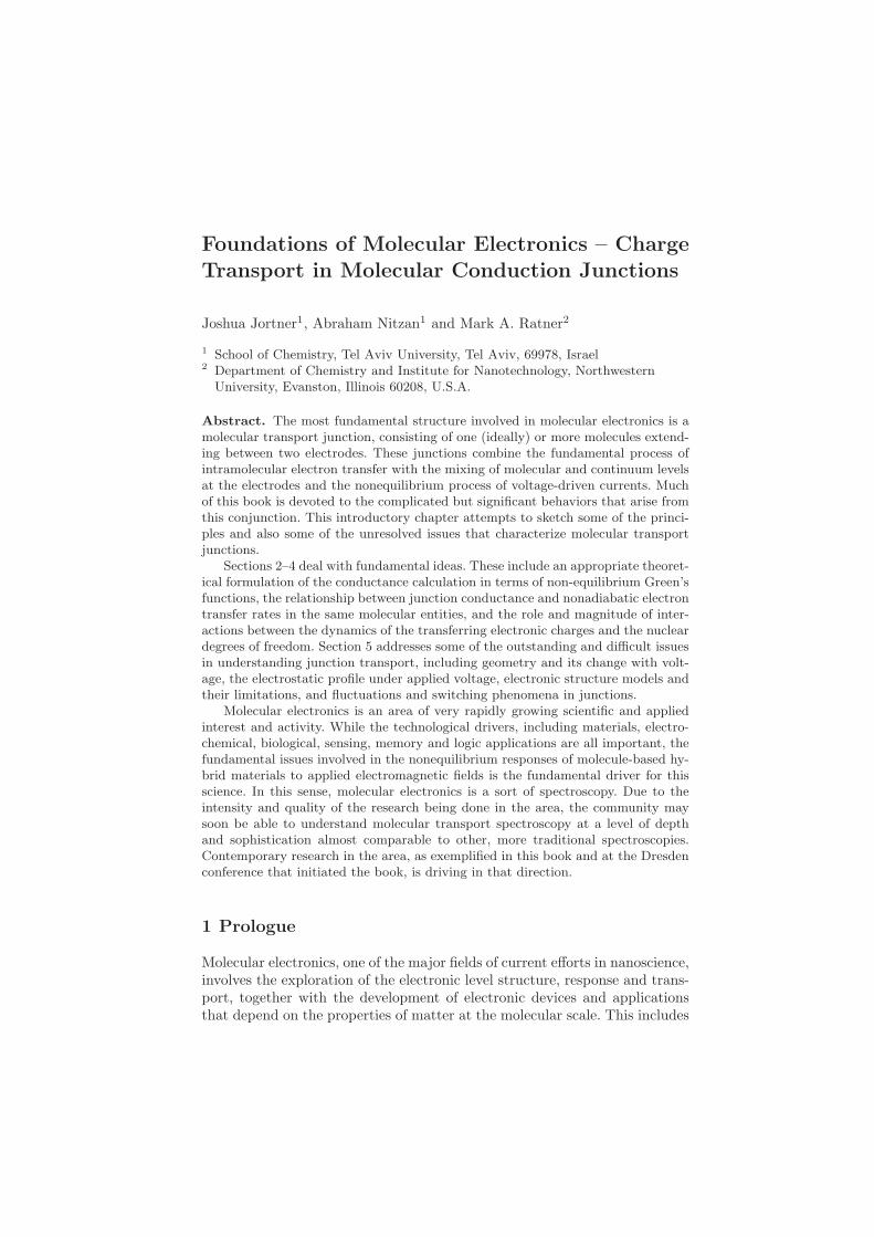
ET theory for donor–acceptor charge transfer represents the non-adiabaticET rate kD→A in the basic form
kD−A = (2π/)V 2F (1)
where V is the effective electronic coupling and F is the thermally aver-aged nuclear vibrational Franck-Condon factor. This microscopic descriptionrests on several ingredients: (1). ET is described as a radiationless transition.(2). The Born-Oppenheimer separability of electronic and nuclear motion ap-plies, enabling the description of the system in terms of diabatic potentialsurfaces Fig. 1 (3). The electronic coupling is sufficiently weak to warrantthe description of the radiationless transition in the non-adiabatic limit. (4).Microscopic ET rates are insensitive to medium dynamics. This state of af-fairs is realized for the common situation of clear separation of time scalesbetween electronic and nuclear processes. (5). Incoherent charge transfer be-tween the donor-acceptor sites, involving dephasing at each ET step. Thisstate of affairs is analogous to Holstein’s small polaron [19] in the incoherentlimit.
The electronic coupling in the DBA system V = VDA+Vsuper consists of asum of a direct D–A exchange contribution VDA between the electronic statesof DA and D
+A
−, and a superexchange off-resonance interaction [20] Vsuper.
The accumulated information concerning the distance dependence of bothdirect and superexchange interactions is that both interactions are expectedto exhibit an exponential distance dependence [21]
V = α exp(−βRDA) , (2)
where RDA is the (either edge-to-edge or center-to-center) D–A distance. Thedistance dependence of intramolecular superexchange interactions in man-made synthetic systems and nature-made biological photosynthetic systems
16 J. Jortner et al.
EaEA
Eb
λλλλ
∆∆∆∆E
energy
ab
Xa Xtr Xb
Fig. 1. A schematic diagram showing the energetics of an electron transfer reactionin terms of two diabatic surfaces, characterized by their curvature, the gap energy∆E and the reorganization energy λ
and in DNA provides a dynamic ruler for the interrogation of the distancedependence of incoherent charge transfer between molecular sites, which aredriven by the electronic coupling with kD→A constrained by the nuclearFranck-Condon factor.
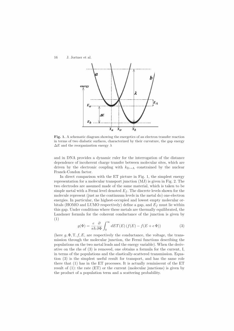
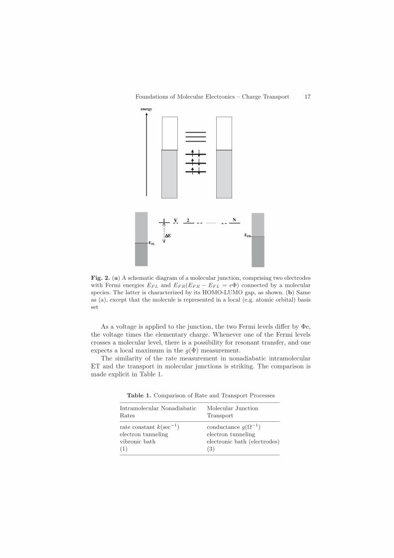
In direct comparison with the ET picture in Fig. 1, the simplest energyrepresentation for a molecular transport junction (MJ) is given in Fig. 2. Thetwo electrodes are assumed made of the same material, which is taken to besimple metal with a Fermi level denoted Ef . The discrete levels shown for themolecule represent (just as the continuum levels in the metal do) one-electronenergies. In particular, the highest-occupied and lowest empty molecular or-bitals (HOMO and LUMO respectively) define a gap, and Ef must lie withinthis gap. Under conditions where these metals are thermally equilibrated, theLandauer formula for the coherent conductance of the junction is given by(1)
g(Φ) =e
π
∂
∂Φ
∫ ∞
0
dET (E) (f(E) − f(E + eΦ)) (3)
(here g,Φ,T, f, E, are respectively the conductance, the voltage, the trans-mission through the molecular junction, the Fermi functions describing thepopulations on the two metal leads and the energy variable). When the deriv-ative on the rhs of (3) is removed, one obtains a formula for the current, I,in terms of the populations and the elastically-scattered transmission. Equa-tion (3) is the simplest useful result for transport, and has the same rolethere that (1) has in the ET processes. It is actually reminiscent of the ETresult of (1): the rate (ET) or the current (molecular junctions) is given bythe product of a population term and a scattering probability.
Foundations of Molecular Electronics – Charge Transport 17
........1 2
∆∆∆∆E
V
EFL
N
E
energy
FR
Fig. 2. (a) A schematic diagram of a molecular junction, comprising two electrodeswith Fermi energies EFL and EFR(EFR − EFL = eΦ) connected by a molecularspecies. The latter is characterized by its HOMO-LUMO gap, as shown. (b) Sameas (a), except that the molecule is represented in a local (e.g. atomic orbital) basisset
As a voltage is applied to the junction, the two Fermi levels differ by Φe,the voltage times the elementary charge. Whenever one of the Fermi levelscrosses a molecular level, there is a possibility for resonant transfer, and oneexpects a local maximum in the g(Φ) measurement.
The similarity of the rate measurement in nonadiabatic intramolecularET and the transport in molecular junctions is striking. The comparison ismade explicit in Table 1.
Table 1. Comparison of Rate and Transport Processes
Intramolecular Nonadiabatic Molecular JunctionRates Transport
rate constant k(sec−1) conductance g(Ω−1)electron tunneling electron tunnelingvibronic bath electronic bath (electrodes)(1) (3)
18 J. Jortner et al.
Since both processes are determined by electron tunneling, they are closelyrelated to one another, as will be discussed in Sect. 3, after a brief descriptionof conductance formulations in Sect. 2. The bath medium, into which theenergy is dissipated, differs from the vibrations and solvent polarization inET to the electrode Fermi sea for simple coherent transport in junctions; thisleads to quite different temperature dependences for the two phenomena.
Section 3 discusses the magnitudes expected for the conductance and forthe rate constants, and presents an analysis of the relationship between thesetwo important observable properties. Section 4 is devoted to behaviors arisingfrom the interactions of the electronic and vibrational degrees of freedom,including inelastic tunneling spectroscopy and the transition from coherentto activated behavior. Section 5 presents a very brief overview of some of theoutstanding issues involved in modeling transport junctions.
Over the past half century the properties of non-molecular electronicmaterials, i.e., metals, semiconductors and dielectrics, and their interfaces,have been investigated extensively and are well understood. Only relativelyrecently was a similar effort directed towards systems involving molecular,mostly organic, materials. During the past decade a new focus on the elec-tronic transport properties of single molecule junctions, as well as molecularand biomolecular DNA chains, is emerging. This research is motivated notonly by envisioned single molecule devices, but also by the conceptual simplic-ity of such systems that offer convenient platforms for correlating theory andexperiment, and by the intrinsic challenge involved in understanding thermo-dynamic response, both electronic and structural, of molecular species in atransport junction.
This book is devoted to the area of molecular electronics, and to explicat-ing and demonstrating some of its crucial understandings, accomplishmentsand challenges. This introductory overview chapter addresses the interrela-tionship among charge transfer, transmission and transport in molecular sys-tems, providing the conceptual framework for molecular electronics. It shouldbe regarded as a sketchy introduction to the field, not a survey. The authorsapologize for the many omissions, and the deeply incomplete literature cita-tions, in this chapter. These should be remedied by the wide scope and depthof this book as an entirety.
2 Theoretical Approaches to Conductance
In this section, we give a brief outline of the standard approaches for model-ing and understanding transport in MJ. Carbon nanotubes, because of theirstiffness and aspect ratio, constitute a special case, and we focus rather onorganic molecules.
The simplest interpretation of Scanning Tunneling Microscope images wasdeveloped by Tersoff and Hamann [22], and states that the current is propor-tional to the total density of states at the position of the terminal atom of the
Foundations of Molecular Electronics – Charge Transport 19
tip and at the Fermi energy. For molecular junctions, this picture is invalid,because the two molecular ends are both in contact with an electrode.
When a molecular structure, acting as a wire, is functionalized to twoelectrodes, a molecular transport junction is formed. The simplest discussionof transport is then to assume that incoming electrons are scattered both atthe interfaces between the metal and the molecule and along the wire itself.Under these conditions, the conductance will depend on the net probabilityof scattering. An important point first noticed by Landauer [23, 24] is thatsuch scattering does not have to be inelastic – even elastic scattering willprevent electrons making it through the junction. Dissipation of energy willeventually occur, but that can happen in the (macroscopic) leads leading tothe molecular junction.
This fundamental realization suggests that the junction resistance in thiscase arises from its behavior as a scatterer, and its conductance can thereforebe calculated simply from scattering theory. This coherent conductance isexpected to characterize most short molecular wires, particularly those inwhich transport occurs far from resonance between the metal Fermi energyand the molecular eigenstates,1 and at low temperature for short wires. Underthose conditions, the conductance g(E, V ) is given by
g(E, V ) =2e2
h
∑ij
tij(E, V ) (4)
Here the prefactor is the quantum of conductance, and tij is the proba-bility that a carrier coming from the left lead in transverse mode i will betransmitted to the right lead in transverse mode j.
A more general approach includes not only elastic scattering, but alsosuch issues as interaction between the molecule and the electrodes and thecoupling to vibrations and to external fields such as light or thermal gradients.The most common formulation is the Keldysh-Kadanoff-Baym [25–28] one interms of non-equilibrium Green’s functions (NEGF). Reference [29–35] Theuse of molecular electronic structure theory for the molecule, combined withmodels for the interface and appropriate treatments (NEGF formulations[29–36], Lippman/Schwinger scattering approaches [37–40]) of the scatteringprocess lead to actual calculations of molecular transport.
In the limit of small applied voltage V , the coherent conductance can bewritten as
g(Φ) =e2
πTrMGM (Φ)ΓR(Φ)GM+
(Φ)ΓL(Φ) (5)
Here the Green’s function GM describes propagation through the mole-cule, and ΓR and ΓL are respectively the spectral densities coupling themolecule to the electrodes on the left and the right. The TrM denotes a
1Near resonance the possibility for dephasing and relaxation may limit the va-lidity of (4)
20 J. Jortner et al.
trace over the states of the molecule, and GM is modified from the baremolecule propagator by including the broadening and shifting effects of themolecule/electrode interactions.
The dependence of the conductance on the molecular species arises mostlyfrom the Green’s function G in (5). In a very simple single-determinant de-scription, if we use i, j to denote atomic orbitals and µ for molecular orbitals,the matrix elements of G are
Gi,j (E) =∑
µ
< i|µ >< µ|j > /(E − Eµ −Σµ ) (6)
with E,Eµ and Σµ respectively the energy variable, the molecular orbitalenergy and the self-energy. The self energy is a complex function – its realpart describes the shift of the resonance due to interaction with the externalpartners, while the imaginary part, Γ, characterizes the lifetime of the state.Note that (as is intuitive) the G will maximize when the injection energy Eis close to a molecular orbital resonance energy Eµ and when the molecularorbital involved has substantial components from the atomic orbitals i, j onthe two ends of the molecule.
A particularly simple junction contains only one homonuclear diatomic(such asH2), with one basis function on each atom. References [3,41] ignoringelectron repulsion and orbital overlap, the two degenerate sites of energy E0
mix by a tunneling energy t0. Then the conductance becomes g(EF ) where
g(E) =e2
π
Γ|t0|2|(E − E0 + (1/2)iΓ)2 − t0|2|2
(7)
When injection occurs exactly on resonance (EF = E0± t0) and t20 Γ 2,this behaves as a pure Landauer channel.
g = g0 = 2e2/h (8)
Note that this holds independent of the spectral density Γ, so long asthe energy E − E0 − t0 overlaps with any nonvanishing value of Γ. Theelastic current for resonance injection is g0, independent of the (nonvanishing)binding between molecule and electrodes. Experimental reports of near-unitconductance for dihydrogen on platinum at low temperatures [42] may reflectsuch injection.
One way to produce resonance injection is to move the molecular eigen-state energies by a gating field. Recent work with a molecular transistor in-jection has indeed observed resonant injection, and g ∼= g0, for such moleculesas ferrocene [43].
Note that if Γ2 t20 but injection is not on resonance (but, say, atmidgap), we find [41]
g = g04t20Γ
2
(t20 + Γ)2→ 0 (9)
Foundations of Molecular Electronics – Charge Transport 21
The conductance then exhibits turnover behavior, vanishing at t0= 0 (as seenfrom (7)) because no mixing of the two molecular sites occurs, and at t0 Γ,because there is no available spectral density at the orbital resonance energy.
3 The Relationship Between Electron Transfer Ratesand Molecular Conduction
We have already noted that electron transfer and molecular conduction aretwo facets of electron transmission through a molecular environment, and assuch should be interrelated. Still this relationship is not a trivial one for sev-eral reasons. First, as discussed in Sect. 1 there are fundamental differencesbetween the two processes that arise from different physical boundary con-ditions. One is driven by nuclear relaxation at the donor and acceptor siteswhile the other is made possible by absorption of the transmitted electronin the continuum of metal electronic states. Secondly, even though the coreprocess in both situations is electron transmission through a molecular layeror bridge, the fact that in the conduction process one puts a potential acrossthe junction may change the electronic structure of the bridge; at the sim-plest level this gives rise to a potential gradient on the bridge itself, implyingchange in local energies. Finally, the two quantities observed, transfer rate inone case and conductance in the other, are different physical observables ofdifferent dimensionalities.
Still, the conduction property of a given molecular system and the elec-tron transfer properties of the same system should be closely related at leastfor low bias potentials and once the different boundary processes have beensorted out. Expression relating the two were recently derived both for the co-herent transport regime and for the incoherent hopping regime. Here we limitourselves to demonstrating the physical issues involved using simple limitingforms. For the coherent transport regime and symmetric electron transfer onefinds [3, 44]
g ≈ 8e2
π2Γ(L)D Γ(R)
A FkD→A (10)
where g is the zero bias conduction, kD→A is the donor-to acceptor electrontransfer rate, F is the Franck-Condon weighted density of states thermal en-vironment (see (1)) and Γ(L)
D and Γ(R)A represent the inverse escape time of
an electron on the donor molecule when next to (say) the left metal elec-trode, into that electrode, and similarly for the acceptor next to the rightmetal electrode. Equation (10) is a limiting form obtained when these ratesare comparable to, or larger than the inverse energy difference between themetal’s Fermi energy and the energy of molecular orbital that is active in thetransport process. Another limiting form is obtained for incoherent hoppingtransfer through a long molecular bridge, provided that energy shifts caused
22 J. Jortner et al.
by the molecule-metal coupling are small relative to kBT . It reads (again forsymmetric electron transfer) [45]
g ≈ e2
kBTkD→A (11)
The simple form of the latter result stems from the fact that for incoherenthopping transmission through a long chain is dominated by dynamics on thechain itself and not at the molecule-lead contacts. Interestingly, and quiteaccidentally, both (10) and (11) yield at room temperature similar numericalestimates
g ∼ (e2/π)(10−13kD→A(S(s−1)) ∼= [10−17kD→A(s−1)]Ω−1 (12)
when the semiclassical Marcus expression [46] for F in a symmetric donor-acceptor problem, F ≈ (
√4πλkBT )−1 exp(−λ/4kBT ) is used in (10) together
with the value λ = 0.5 eV for the reorganization energy and the valuesΓ(L)
D = Γ(R)A ∼ 0.5 eV for the electron escape rates into the electrodes. Actual
values of these parameters can of course differ, but these representative valuesprovide an order-of-magnitude criterion for observing conduction in the smallvoltage-bias regime of molecular conduction junctions. For example, with acurrent detector sensitive to pico-amperes, kD→A has to exceed ∼106 s−1 (forthe estimates of F and Γ given above) before measurable current can be ob-served at 0.1V across such a junction. Such estimates should be exercisedwith caution, both because the above expressions are approximate limitingforms of more complex relationships within the corresponding models andbecause the models themselves are highly simplified. Still, they may be use-ful as rough order of magnitude estimates as was indeed found in a recentcomparison of electron transfer and conduction through alkane bridges [47].
4 Interaction with Nuclear Degrees of Freedom
Electron transfer processes, as described in Sect. 1 involve electron-phononcoupling in an essential way: this coupling causes the relaxation process thataffects electron localization on the donor and acceptor species and therebydrives the transfer process. As discussed in Sect. 2, molecular conduction isdriven by a potential difference between two infinite electrodes and phononinduced localization does not play any essential role in affecting this driving.Still, also in molecular conduction, the coupling between electronic and nu-clear degrees of freedom is of great interest on several counts. First, it under-lines the interplay between coherent transport by carrier tunneling and/orband motion, polaronic conduction and incoherent, thermally assisted hop-ping transport [3]. Indeed, the importance of the full hopping regime, in whichcharges are definitely localized on the molecular bridge, has been demon-strated both in the Coulomb blockade limit [48] and in a polaron-type local-ization situation [49]. Secondly, it is directly relevant to the issue of junction
Foundations of Molecular Electronics – Charge Transport 23
heating [50–52]. Also, vibronic interactions accompanying electron transportmay lead to specific nuclear motions such as rotations [53, 54], lateral hop-ping of molecules on the surface [55], atomic rearrangements [56] and chemicalreactions [57]. Finally, nuclear motions can directly manifest themselves asinelastic signals in the current-voltage spectra. Inelastic electron tunnelingspectroscopy (IETS) has been an important tool for identifying molecularspecies in tunnel junctions for a long time [58]. With the development andadvances in scanning tunneling microscopy (STM) and spectroscopy (STS)it has proven invaluable as a tool for identifying and characterizing molecu-lar species within the conduction region [54, 59–62]. Indeed, this is the onlydirect way to ascertain that a molecular species indeed participates in theconduction process, and at the same time to provide important spectroscopicand structural data on the conducting molecule, in particular information onthe strength of the vibronic coupling itself [63].
4.1 Timescale Issues
The relative importance of vibronic (or electron-phonon) interactions in elec-tron transmission processes is an issue of relative timescales. If the trans-mission event is fast on the timescale of nuclear motion the latter may betaken static, and we only need to average the resulting elastic transmissionprobability over the relevant ensemble of nuclear configurations. The other ex-treme limit, where the nuclear motion is fast relative to the electronic processis usually not relevant in our system. Dynamic electron-phonon effects maypotentially play a significant role when the electronic and nuclear timescaleare similar. In order to make an assessment of this possibility an estimateof the relevant electronic timescale is needed. For resonance electron transferthis timescale is associated with the electronic coupling, e.g. for band motion– by the inverse bandwidth. For off resonance tunneling transmission a usefulestimate is provided by the tunneling traversal time, τtrav, essentially a (non-rigorous) estimate of the time available for a tunneling electron to interactwith degrees of freedom localized in the barrier region. For example, for aparticle of mass m and energy E that tunnel through a rectangular barrierof height U and width D, the traversal time is given by
τtrav =√
m
2(U − E)D (13)
while for transmission in the model of Fig. 2b, involving N bridge levels andan energy gap ∆E we obtain [64]
τtrav =N
E (14)
It may in fact be shown [64] that both (13) and (14) are limiting cases of amore general expression. For typical molecular parameters, say D = 1 nm,
24 J. Jortner et al.
N ∼= 2 − 4 and ∆E = U − E = 1V (13) and (14) yield τtrav in the range0.1 − 1 fs. On this short timescale one may disregard nuclear motion andinelastic effects on electron transmission. We see however that for smaller∆E inelastic effects may become relevant. In particular this is often the casein resonance tunneling situations. For example, a recent computational studyof electron tunneling through water films [65] has revealed the existence ofwater structures that support resonance tunneling in the energy range of upto 1 eV below the vacuum barrier and with traversal timescales of the orderof ∼10 fs, similar to the period of the OH stretch vibrations in water.
4.2 Transition from Coherent to Incoherent Motion
In most treatments of electron transmission and conduction through insu-lating barriers one assumes that the barrier nuclear configuration is static.(This should be distinguished from nuclear relaxation at the donor and ac-ceptor sites in the electron transfer process which is the driving force forthis process). The breakdown of this assumption can potentially have farreaching consequences. In the extreme case, energy transfer into nuclear mo-tions from the transmitting electrons may lead to conformation changes andeventually to disintegration of the junction. Indeed, an important factor indesigning molecular conductors is their structural stability and understand-ing processes that can undermine this stability is of utmost importance [66].A single molecule junction that carries 1 nA of current over a voltage dropof 1 volt passes ∼1010 eV of energy per second, many orders of magnitudemore than is needed to atomize its components. This implies the need forunderstanding heat generation and dissipation in molecular conductors. Inthe other limit of very weak electron-nuclear interaction, electron transferand transmission remain essentially the same, still the signature of electron-phonon coupling may be observed as vibrational features in the voltage de-pendence of the current observed in inelastic tunneling spectroscopy.
In very common intermediate cases, energy does not accumulate exces-sively in the junction, still interactions with the thermal environments canlead to a fundamental change in the transmission mechanism: Coherent trans-fer is replaced by incoherent hopping. This can be simply demonstrated [29],for a one dimensional wire problem where, in the linear transport regime, theLandauer formula [29] for the conduction reads
g(E) =e2
πT (15)
where T is the transmission coefficient and e the electron charge. Considernow a conductor of length L as a series of N macroscopic scatterers. At eachscatterer the electron can be transmitted with probability T , or reflectedwith probability P = 1 − T . Let the the total transmission through N suchobjects be TN , so that T = T1. Provided that the phase of the wavefunc-tion is destroyed after each transmission-reflection event, so that we can add
Foundations of Molecular Electronics – Charge Transport 25
probabilities, the transmission through an N scatterers system is obtainedby considering a connection in series of an N − 1 scatterer system with anadditional scatterer, and summing over all multiple scattering paths
TN = TN−1(1 + RRN−1 + (RRN−1)2 + . . .)T =T TN−1
1 −RRN−1(16)
with R = 1 − T and RN = 1 − TN . This implies
1 − TN
TN=
1 − TN−1
TN−1+
1 − TT = N
1 − TT (17)
so thatTN =
TN(1 − T ) + T =
L0
L+ L0(18)
where L0 = T /V (1 − T and v = N/L is the scatterer density. Using thistransmission coefficient in (15) yields
g(E) =e2
π
L0
L+ L0(19)
that gives the inverse length dependence characteristic of Ohm’s law as L→∞.
More detailed treatments can handle situations where dephasing is notcomplete at each scatterer. Buttiker [67] has introduced phase destructionprocesses by conceptually attaching an electron reservoir onto the constrictionunder the condition that, while charge carriers are exchanged between thecurrent-carrying system and the reservoir, no net averaged current is flowinginto this reservoir. Such a contact, essentially a voltage probe, acts as a phasebreaking scatterer, and the dephasing efficiency is controlled by adjustingthe coupling strength between this device and the system. A very differentapproach to dephasing was considered by Bixon and Jortner [68, 69] whopointed out that the irregular nature of Franck Condon overlaps betweenintramolecular vibrational states associated with different electronic centerscan lead to phase erosion in resonant electron transfer. Yet another approachuses the machinery of non-equilibrium statistical mechanics, starting froma Hamiltonian that includes the junction and its thermal environment andderiving reduced equations of motion for the electron dynamics. This leadsto a dynamical description that includes the effect of dephasing and energyrelaxation that are characterized by properties of the thermal bath and thesystem-bath coupling.
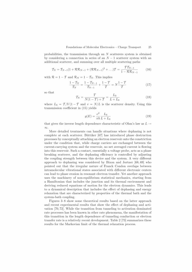
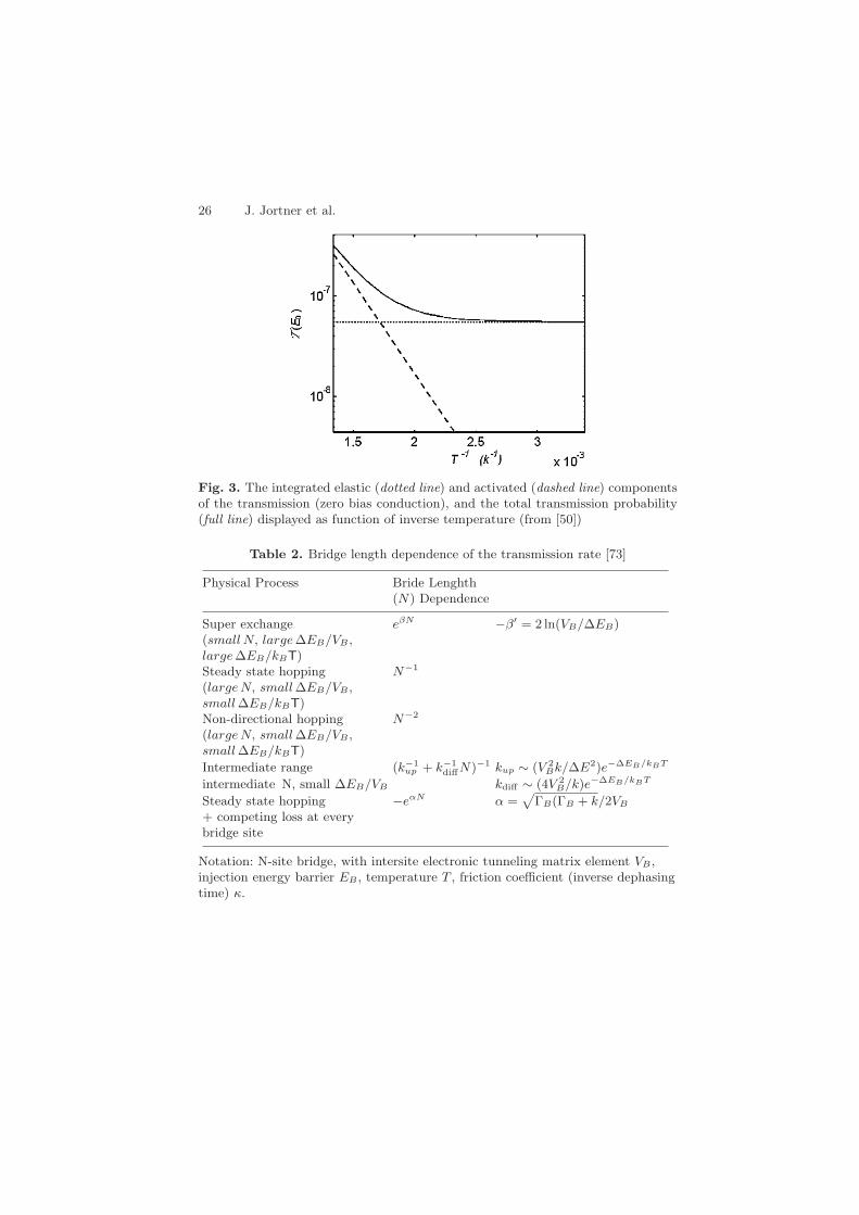
Figures 3–8 show some theoretical results based on the latter approachand recent experimental results that show the effect of dephasing and acti-vation [70, 72]. While the transition from tunneling to activation dominatedrate processes has been known in other rate phenomena, the manifestation ofthis transition in the length dependence of tunneling conduction or electrontransfer rate is a relatively recent development. Table 2 [73] summarizes theseresults for the Markovian limit of the thermal relaxation process.
26 J. Jortner et al.
Fig. 3. The integrated elastic (dotted line) and activated (dashed line) componentsof the transmission (zero bias conduction), and the total transmission probability(full line) displayed as function of inverse temperature (from [50])
Table 2. Bridge length dependence of the transmission rate [73]
Physical Process Bride Lenghth(N) Dependence
Super exchange eβN −β′ = 2 ln(VB/∆EB)(small N, large ∆EB/VB ,large ∆EB/kBT)Steady state hopping N−1
(large N, small ∆EB/VB ,small ∆EB/kBT)Non-directional hopping N−2
(large N, small ∆EB/VB ,small ∆EB/kBT)
Intermediate range (k−1up + k−1
diffN)−1 kup ∼ (V 2Bk/∆E2)e−∆EB/kBT
intermediate N, small ∆EB/VB kdiff ∼ (4V 2B/k)e−∆EB/kBT
Steady state hopping −eαN α =√
ΓB(ΓB + k/2VB
+ competing loss at everybridge site
Notation: N-site bridge, with intersite electronic tunneling matrix element VB ,injection energy barrier EB , temperature T , friction coefficient (inverse dephasingtime) κ.
Foundations of Molecular Electronics – Charge Transport 27
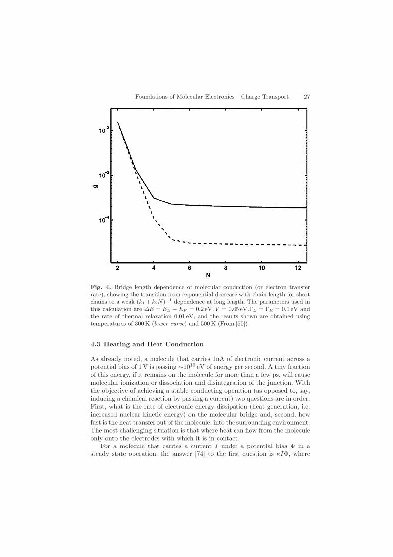
Fig. 4. Bridge length dependence of molecular conduction (or electron transferrate), showing the transition from exponential decrease with chain length for shortchains to a weak (k1 + k2N)−1 dependence at long length. The parameters used inthis calculation are ∆E = EB − EF = 0.2 eV, V = 0.05 eV.ΓL = ΓR = 0.1 eV andthe rate of thermal relaxation 0.01 eV, and the results shown are obtained usingtemperatures of 300 K (lower curve) and 500K (From [50])
4.3 Heating and Heat Conduction
As already noted, a molecule that carries 1nA of electronic current across apotential bias of 1V is passing ∼1010 eV of energy per second. A tiny fractionof this energy, if it remains on the molecule for more than a few ps, will causemolecular ionization or dissociation and disintegration of the junction. Withthe objective of achieving a stable conducting operation (as opposed to, say,inducing a chemical reaction by passing a current) two questions are in order.First, what is the rate of electronic energy dissipation (heat generation, i.e.increased nuclear kinetic energy) on the molecular bridge and, second, howfast is the heat transfer out of the molecule, into the surrounding environment.The most challenging situation is that where heat can flow from the moleculeonly onto the electrodes with which it is in contact.
For a molecule that carries a current I under a potential bias Φ in asteady state operation, the answer [74] to the first question is κIΦ, where
28 J. Jortner et al.
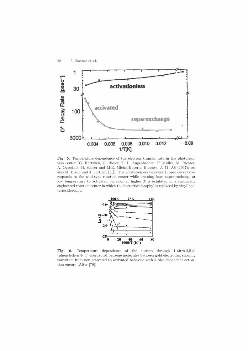
Fig. 5. Temperature dependence of the electron transfer rate in the photoreac-tion center (G. Hartwich, G. Bieser, T. L. Angenbachen, P. Muller, M. Richter,A. Ogrodnik, H. Scheer and M.E. Michel-Beyerle, Biophys. J. 71, A8 (1997); seealso M. Bixon and J. Jortner, [11]). The activationless behavior (upper curve) cor-responds to the wild-type reaction center while crossing from super-exchenge atlow temperature to activated behavior at higher T is exhibited in a chemicallyengineered reaction center in which the bacteriochlorophyl is replaced by vinyl bac-teriochlorophyl
Fig. 6. Temperature dependence of the current through 1-nitro-2,5-di(phenylethynyl- 4’ -mercapto) benzene molecules between gold electrodes, showingtransition from non-activated to activated behavior with a bias-dependent activa-tion energy (After [70])
Foundations of Molecular Electronics – Charge Transport 29
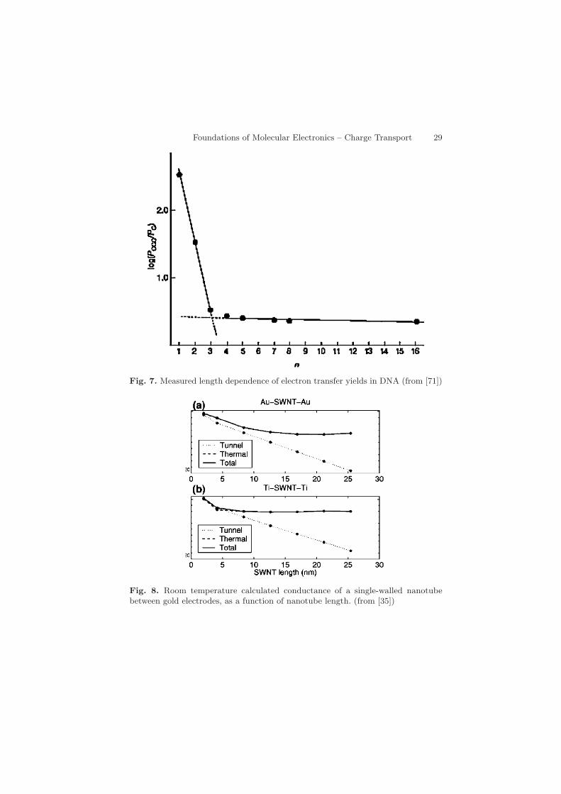
Fig. 7. Measured length dependence of electron transfer yields in DNA (from [71])
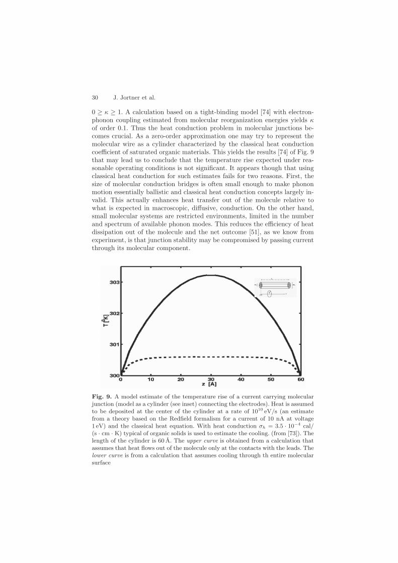
Fig. 8. Room temperature calculated conductance of a single-walled nanotubebetween gold electrodes, as a function of nanotube length. (from [35])
30 J. Jortner et al.
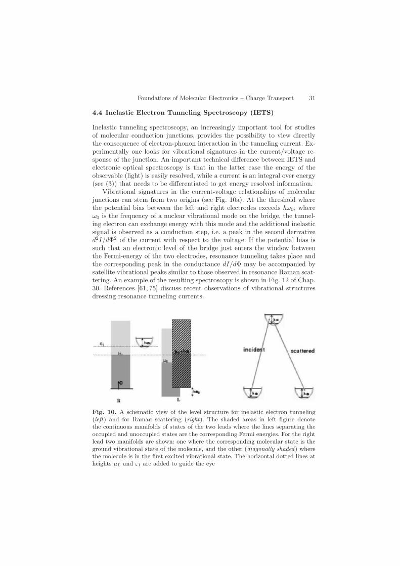
0 ≥ κ ≥ 1. A calculation based on a tight-binding model [74] with electron-phonon coupling estimated from molecular reorganization energies yields κof order 0.1. Thus the heat conduction problem in molecular junctions be-comes crucial. As a zero-order approximation one may try to represent themolecular wire as a cylinder characterized by the classical heat conductioncoefficient of saturated organic materials. This yields the results [74] of Fig. 9that may lead us to conclude that the temperature rise expected under rea-sonable operating conditions is not significant. It appears though that usingclassical heat conduction for such estimates fails for two reasons. First, thesize of molecular conduction bridges is often small enough to make phononmotion essentially ballistic and classical heat conduction concepts largely in-valid. This actually enhances heat transfer out of the molecule relative towhat is expected in macroscopic, diffusive, conduction. On the other hand,small molecular systems are restricted environments, limited in the numberand spectrum of available phonon modes. This reduces the efficiency of heatdissipation out of the molecule and the net outcome [51], as we know fromexperiment, is that junction stability may be compromised by passing currentthrough its molecular component.
Fig. 9. A model estimate of the temperature rise of a current carrying molecularjunction (model as a cylinder (see inset) connecting the electrodes). Heat is assumedto be deposited at the center of the cylinder at a rate of 1010 eV/s (an estimatefrom a theory based on the Redfield formalism for a current of 10 nA at voltage1 eV) and the classical heat equation. With heat conduction σh = 3.5 · 10−4 cal/(s · cm · K) typical of organic solids is used to estimate the cooling. (from [73]). Thelength of the cylinder is 60 A. The upper curve is obtained from a calculation thatassumes that heat flows out of the molecule only at the contacts with the leads. Thelower curve is from a calculation that assumes cooling through th entire molecularsurface
Foundations of Molecular Electronics – Charge Transport 31
4.4 Inelastic Electron Tunneling Spectroscopy (IETS)
Inelastic tunneling spectroscopy, an increasingly important tool for studiesof molecular conduction junctions, provides the possibility to view directlythe consequence of electron-phonon interaction in the tunneling current. Ex-perimentally one looks for vibrational signatures in the current/voltage re-sponse of the junction. An important technical difference between IETS andelectronic optical spectroscopy is that in the latter case the energy of theobservable (light) is easily resolved, while a current is an integral over energy(see (3)) that needs to be differentiated to get energy resolved information.
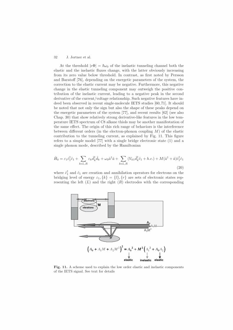
Vibrational signatures in the current-voltage relationships of molecularjunctions can stem from two origins (see Fig. 10a). At the threshold wherethe potential bias between the left and right electrodes exceeds ω0, whereω0 is the frequency of a nuclear vibrational mode on the bridge, the tunnel-ing electron can exchange energy with this mode and the additional inelasticsignal is observed as a conduction step, i.e. a peak in the second derivatived2I/dΦ2 of the current with respect to the voltage. If the potential bias issuch that an electronic level of the bridge just enters the window betweenthe Fermi-energy of the two electrodes, resonance tunneling takes place andthe corresponding peak in the conductance dI/dΦ may be accompanied bysatellite vibrational peaks similar to those observed in resonance Raman scat-tering. An example of the resulting spectroscopy is shown in Fig. 12 of Chap.30. References [61, 75] discuss recent observations of vibrational structuresdressing resonance tunneling currents.
Fig. 10. A schematic view of the level structure for inelastic electron tunneling(left) and for Raman scattering (right). The shaded areas in left figure denotethe continuous manifolds of states of the two leads where the lines separating theoccupied and unoccupied states are the corresponding Fermi energies. For the rightlead two manifolds are shown: one where the corresponding molecular state is theground vibrational state of the molecule, and the other (diagonally shaded) wherethe molecule is in the first excited vibrational state. The horizontal dotted lines atheights µL and ε1 are added to guide the eye
32 J. Jortner et al.
At the threshold |eΦ| = ω0 of the inelastic tunneling channel both theelastic and the inelastic fluxes change, with the latter obviously increasingfrom its zero value below threshold. In contrast, as first noted by Perssonand Baratoff [76], depending on the energetic parameters of the system, thecorrection to the elastic current may be negative. Furthermore, this negativechange in the elastic tunneling component may outweigh the positive con-tribution of the inelastic current, leading to a negative peak in the secondderivative of the current/voltage relationship. Such negative features have in-deed been observed in recent single-molecule IETS studies [60,71]. It shouldbe noted that not only the sign but also the shape of these peaks depend onthe energetic parameters of the system [77], and recent results [62] (see alsoChap. 30) that show relatively strong derivative-like features in the low tem-perature IETS spectrum of C8 alkane thiols may be another manifestation ofthe same effect. The origin of this rich range of behaviors is the interferencebetween different orders (in the electron-phonon coupling M) of the elasticcontribution to the tunneling current, as explained by Fig. 11. This figurerefers to a simple model [77] with a single bridge electronic state (1) and asingle phonon mode, described by the Hamiltonian
H0 = ε1c†1c1 +
∑kεL,R
εkd†kdk + ω0a
†a+∑
kεL,R
(Vk1d†k c1 + h.c.) +M(a† + a)c†1c1
(20)where c†1 and c1 are creation and annihilation operators for electrons on thebridging level of energy ε1, k = l, r are sets of electronic states rep-resenting the left (L) and the right (R) electrodes with the corresponding
electrons
vibrations M
A0A1M
A2M2
(((( )))) (((( ))))1 1
2 2 2 202 20
20A AA MA M AA AM+ ++ ++ ++ + ++++==== ++++
elastic inelastic elastic
Fig. 11. A scheme used to explain the low order elastic and inelastic componentsof the IETS signal. See text for details
Foundations of Molecular Electronics – Charge Transport 33
creation and annihilation operators d†k and dk and a†k and a are creation andannihilation operator for the phonon mode of frequency ω0. The tunnelingamplitude may be written, to second order in the electron-phonon couplingM as A = A0 + A1M + A2M
2 where A0 is the amplitude of a zero orderprocess that involves no phonons, A1 is a 1-phonon inelastic tunneling am-plitude and A2 is a 2-phonon elastic amplitude that describes a second orderprocess where one phonon was created then destroyed. Clearly, the intensityA2 contains in second order contributions of inelastic process, and interferingelastic processes as seen in Fig. 11.
5 Remarks and Generalities
Since junction transport is in some senses an extension of non-adiabatic mole-cular electron transfer, conductances and rate constants are closely related(Sect. 3), and both undergo characteristic changes between coherent and in-coherent motion mechanisms (Sect. 4). Because of these similarities, thereare a number of common issues that will arise in the measurement of eitherconductance or electron transfer rates. These are discussed in Sect. 5.1 ofthis chapter. There are, however, some special aspects of junction transport,that arise from the nature of the states and the dynamical processes involved.These aspects are discussed in Sect. 5.2.
5.1 Electron Transfer and Conductance: Common Issues
Electronic States
Because charge transfer or transport is the defining process, both ET andJC (electron transfer and junction conductance) deal with initial and finalelectronic states. In junctions, the electronic states in question lie within thecontinuum of the leads. For ET, both the initial and final states are isolatedmolecule electronic eigenstates. Nevertheless, the transport coefficients (kET
and g) will vary with varying initial or final electronic state. While this hasbeen extensively investigated in the ET field [1, 78, 79] (in particular usingphotoelectrochemistry), it is also expected to be present in junctions: indeed,photoexcited junction transport has been discussed in the theoretical litera-ture [80], and some initial experimental aspects are beginning to appear [81].
Electron Correlation
The electron correlation problem enters into both processes. This term refersto the fact that interelectron repulsion both makes the electronic structure ofmolecules or solids a problem that is impossible to solve exactly, and substan-tively modifies energy levels. In most treatments of ET or MJ, a major simpli-fication is made in that only the single electron terms of a model Hamiltonian
34 J. Jortner et al.
are used: these models are sometimes called tight binding [82], or extendedHuckel or one electron. Electron repulsions cause major changes in the prop-erties of individual molecules (for example, they change the optical spectraqualitatively, they are responsible for bond formation and taking them intoaccount is the dominant reason why electronic structure calculations in 2004are better than they were in 1946).
Calculations employing electronic correlation, often using density func-tional theory, are now becoming standard both in transport [29–41, 83] andin transfer, but nevertheless major problems still inhere in dealing correctlywith the effects of correlation. A specific instance involving junction behaviorwill be discussed in Sect. 5.2.
Spin Effects
Because of the Exclusion Principle, interactions between same spin and oppo-site spin electrons are different. In ET, these spin effects are strongly markedin situations involving particular open shell transition metal ions, notablycobalt. In junction transport, there have been a number of theoretical analy-ses of possible spin effects [84]: one idea is that the spins are polarized inthe metallic electrode, and the amplitude for scattering through the junctionfor same spin and differing spin electrons will differ. The opposite limit in-volves non-singlet states on the molecule itself. No experimental observationsof such phenomena are yet reported. There is also an interesting issue of spinquantization axis, since the two electrodes and the molecule might have quitediffering spin axes.
Geometry
It has already been stressed that to obtain useful structure/function rela-tionships, one needs to know structure. Electronic structure calculation forindividual molecules can give bond lengths and bond angles, for stable or-ganics, that are essentially as exact as experiment. For ET reactions, then,the geometry problem is to some extent computationally solved. In starkcontrast, with the possible exception of nanotubes, nearly nothing is knownexperimentally about the actual geometry of molecules in transport junc-tions: this is a non-equilibrium situation, and non-equilibrium methods arerequired to calculate such geometries. There have been some attempts in thisdirection [85], but since experimental determination of the geometries is sovery difficult, it is not known how accurate such calculations are.
5.2 Junction Conductance
Because ET is one of the most important reactions in chemistry, the issuesdiscussed in Sect. 5.1 of this chapter have been investigated there both theo-retically and experimentally. Since studies of JC are essentially only a decade
Foundations of Molecular Electronics – Charge Transport 35
old, and since the metrical problems are so serious, much of this territory hasbeen unexplored. But other effects can dominate in junction transport, andthese differentiate the ET and JC situations.
Geometric Behavior
Modifications in structure lead to modifications in molecular properties; suchstructure/function relationships are at the heart of modern chemistry. InJC, as already stated several times, the geometries are effectively unknown,and indeed there does not seem any direct scattering method that can beused experimentally to find accurately the geometry of a molecule madeof first row atoms in the presence of a large number of metal or semicon-ductor atoms constituting the electrode. Indirect structural analysis, usingvibrational spectroscopy and scanning probe information, is becoming avail-able [62,86]. Until such geometric information permits comparison with com-putations both of the structure and of transport with different structures,this will comprise a very serious difficulty for accurate comparison betweenmodeling and experiments. Beautiful experiments have demonstrated thatelectronic currents in junctions can actually break chemical bonds, excitevibrations, and otherwise alter the structural chemistry of the molecules ofthese junctions [53,54,57,59–61,74]. Understanding that variation remains amajor task.
Voltage Profiles
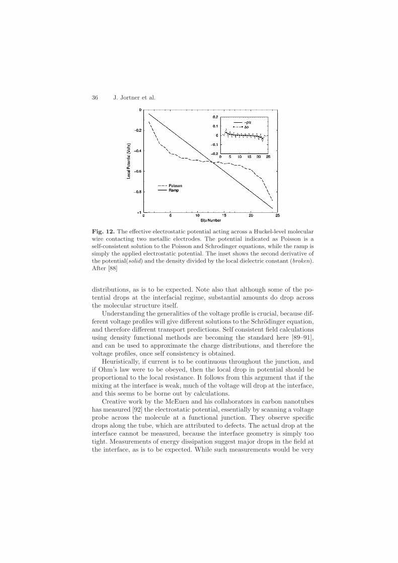
The issue of voltage profiles, effectively the electrochemical potential across ajunction in a non-equilibrium state, can be crucial in determining behaviors.This has been studied beginning with a clarification by Datta and his collab-orators of the importance of the voltage drop structure [87]. Figure 12 showssome calculations of the local electrostatic field across a model wire systemin the Huckel drescription [88]: notice the change in shape from the simpleramp (which is correct in the absence of any charge within the junctions)to a highly screened interaction in which most of the field drops at the elec-trode/molecule interface. The extent to which a voltage drop occurs at anygiven spot can only be determined by a self consistent calculation that takesinto account carrier-carrier interactions, because it is necessary to solve si-multaneously the Poisson equation for the electrostatics and the Schrodingerequation for the wave function. The smooth curves in Fig. 12 come fromsolving these equations simultaneously for a simple junction model of a wire.In more extensive calculations on the molecules, there have been attempts todescribe the electrostatics. Figure 13 shows the calculated electrostatics fora junction consisting of an organic between gold electrodes [89]. There aresubstantial changes in the potential due to the presence of electrical charge
36 J. Jortner et al.
Fig. 12. The effective electrostatic potential acting across a Huckel-level molecularwire contacting two metallic electrodes. The potential indicated as Poisson is aself-consistent solution to the Poisson and Schrodinger equations, while the ramp issimply the applied electrostatic potential. The inset shows the second derivative ofthe potential(solid) and the density divided by the local dielectric constant (broken).After [88]
distributions, as is to be expected. Note also that although some of the po-tential drops at the interfacial regime, substantial amounts do drop acrossthe molecular structure itself.
Understanding the generalities of the voltage profile is crucial, because dif-ferent voltage profiles will give different solutions to the Schrodinger equation,and therefore different transport predictions. Self consistent field calculationsusing density functional methods are becoming the standard here [89–91],and can be used to approximate the charge distributions, and therefore thevoltage profiles, once self consistency is obtained.
Heuristically, if current is to be continuous throughout the junction, andif Ohm’s law were to be obeyed, then the local drop in potential should beproportional to the local resistance. It follows from this argument that if themixing at the interface is weak, much of the voltage will drop at the interface,and this seems to be borne out by calculations.
Creative work by the McEuen and his collaborators in carbon nanotubeshas measured [92] the electrostatic potential, essentially by scanning a voltageprobe across the molecule at a functional junction. They observe specificdrops along the tube, which are attributed to defects. The actual drop at theinterface cannot be measured, because the interface geometry is simply tootight. Measurements of energy dissipation suggest major drops in the field atthe interface, as is to be expected. While such measurements would be very
Foundations of Molecular Electronics – Charge Transport 37
helpful for small molecule circuits, the short length (∼1 nm) makes them verydifficult.
The simplest way to think about such effects is to consider that moleculesact like polarizable capacitors in junctions, and that the molecular charge dis-tribution polarizes itself to offset the applied field. In this sense, the interfacelooks slightly like an electrochemical double layer.
The superexchange mechanisms, as detailed above, suggest that whichevereffectively coupled frontier level is closer in energy to the injection energy inthe junction case, or closer in energy to the donor in the ET case, shoulddominate the rate constant. Analysis is more difficult with the junctions, onlybecause so many levels of the “extended molecules” enter. For example, veryrecent calculations by the Bredas Group [93] and by Basch and collaborators[93] have demonstrated that the effective levels of the extended molecule arenot the HOMO and the LUMO, because of the importance of metal-inducedgap states [94]. Important, strongly coupled levels can be found by populationanalysis, and for the simple benzenedithiol case there are of the order of adozen intervening in the extended molecule [93].
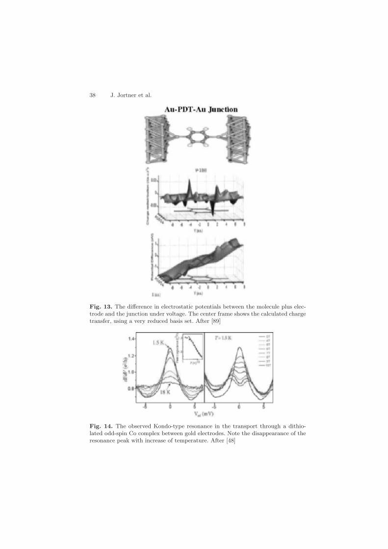
Classically, one expects that the presence of a charge distribution near ametal will result in polarization of the metal, and that this polarization canbe well described in terms of an image potential picture. Computationally,using electronic structure methods to calculate this image is difficult [96],essentially because of the interelectronic repulsions in the metal. It is notclear how well any of the “extended molecule” schemes currently in vogue forcalculating junction transport deal with the very important image problem,nor is it really clear how to include the image heuristically (double countingof image effects must be avoided). Very recent work by the Purdue group [95]has used a self consistent solution to the Poisson equation with an imagecorrection, within a semiempirical CNDO model Hamiltonian. They calculateboth the effective voltage profile and the I/V characteristics. The resultsshow rectification behavior, agreeing very well with break junction transportmeasurements [99].
Electron Correlation
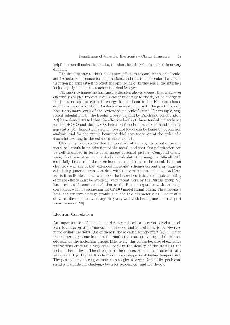
An important set of phenomena directly related to electron correlation ef-fects is characteristic of mesoscopic physics, and is beginning to be observedin molecular junctions. One of these is the so called Kondo effect [48], in whichthere is actually a maximum in the conductance at zero voltage, if there is anodd spin on the molecular bridge. Effectively, this comes because of exchangeinteractions creating a very small peak in the density of the states at themetallic Fermi level. The strength of these interactions is characteristicallyweak, and (Fig. 14) the Kondo maximum disappears at higher temperature.The possible engineering of molecules to give a larger Kondo-like peak con-stitutes a significant challenge both for experiment and for theory.
38 J. Jortner et al.
Fig. 13. The difference in electrostatic potentials between the molecule plus elec-trode and the junction under voltage. The center frame shows the calculated chargetransfer, using a very reduced basis set. After [89]
Fig. 14. The observed Kondo-type resonance in the transport through a dithio-lated odd-spin Co complex between gold electrodes. Note the disappearance of theresonance peak with increase of temperature. After [48]
Foundations of Molecular Electronics – Charge Transport 39
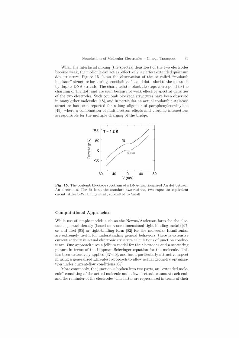
When the interfacial mixing (the spectral densities) of the two electrodesbecome weak, the molecule can act as, effectively, a perfect extended quantumdot structure. Figure 15 shows the observation of the so called “coulombblockade” structure for a bridge consisting of a gold dot linked to the electrodeby duplex DNA strands. The characteristic blockade steps correspond to thecharging of the dot, and are seen because of weak effective spectral densitiesof the two electrodes. Such coulomb blockade structures have been observedin many other molecules [48], and in particular an actual coulombic staircasestructure has been reported for a long oligomer of paraphenylenevinylene[49], where a combination of multielectron effects and vibronic interactionsis responsible for the multiple charging of the bridge.
V (mV)-80
data
fit
T = 4.2 K
Cur
rent
(pA
)
-40 0 40 80
50
0
-50
100
Fig. 15. The coulomb blockade spectrum of a DNA-functionalized Au dot betweenAu electrodes. The fit is to the standard two-resistor, two capacitor equivalentcircuit. After S-W. Chung et al., submitted to Small
Computational Approaches
While use of simple models such as the Newns/Anderson form for the elec-trode spectral density (based on a one-dimensional tight binding metal) [97]or a Huckel [95] or tight-binding form [82] for the molecular Hamiltonianare extremely useful for understanding general behaviors, there is extensivecurrent activity in actual electronic structure calculations of junction conduc-tance. One approach uses a jellium model for the electrodes and a scatteringpicture in terms of the Lippman-Schwinger equation for the molecule. Thishas been extensively applied [37–40], and has a particularly attractive aspectin using a generalized Ehrenfest approach to allow actual geometry optimiza-tion under current-flow conditions [85].
More commonly, the junction is broken into two parts, an “extended mole-cule” consisting of the actual molecule and a few electrode atoms at each end,and the reminder of the electrodes. The latter are represented in terms of their
40 J. Jortner et al.
surface Green’s functions, and act as source and drain. The extended mole-cule is treated using a chosen electronic structure model [29–36]. The choiceof method and the basis set determines the quality of the calculation, andself-consistent solution of transport and electronic structure allows predictionof the voltage-dependent conductance. Usually, some form of static DensityFunctional Theory (DFT) is used for the electronic structure problem.
There are substantive difficulties here, including the fact that static DFTdoes a very poor job of representing electron injection or ionization processes(essentially the content of the G in (5)), and the balance problem between thebasis sets on the molecule and the metal atoms [83,98]. Several contributionsboth in this book and elsewhere [98] describe alternate, sometimes moresophisticated electronic structure approaches. Since ab-initio methods usingcorrelation corrections of the coupled cluster or Moller-Plesset type do aquite good job in describing ionization and electron capture, their use forconductance seems promising. Basis set issues might be simplified by goingto plane-wave formulations.
Reliability, Reproducibility, Experimental Conditionsand Switching
Because junction transport is such a new measurement, the community con-tinues to seek the most effective ways to make voltage spectroscopic mea-surements of transport. Several of the important schemes for doing so willbe outlined in the following chapters of this book. In general, however, themeasurements break down into two major categories. First, there are breakjunction measurements [42,99,100], fabrication schemes [101], particular lim-its of crossed-wire, STM and nanodot collection measurements [102–104], inwhich one is presumably measuring a small number (ideally 1) of molecules.Second are measurements on adlayers, in which many thousands of moleculescan contribute to the transport [105, 106]. There is no necessary reason whythese two sorts of measurement should give the same current/voltage signa-tures, even if the molecules are identical, and the electrodes are identical [107].There are several reasons why such disparities might exist:
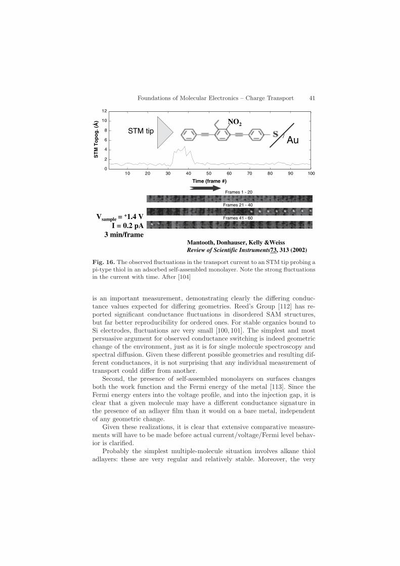
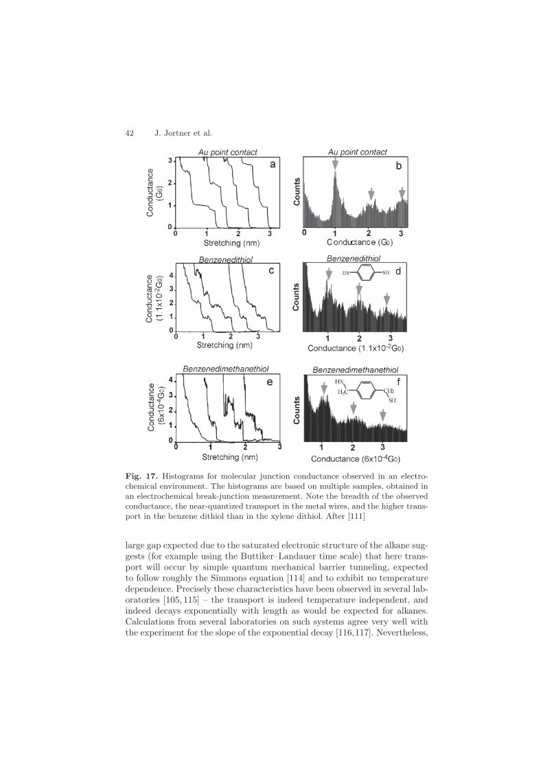
First, the spectral densities (effective inverse contact resistance) couldvary between adlayers and single molecules. Indeed, calculations indicate[108] (and measurements of adlayer stability and motion also suggest [109]that there are several stable sites for the most common geometries, suchas thiol/gold or siloxy linkages [110]. These different geometries are alsocalculated to have different spectral densities, and therefore different con-ductance signatures [108]. This is almost certainly the reason for the often-observed striking switching in time dependent measurements of transport.Figure 16 shows an important contribution from the Weiss laboratory [104],with switching on and switching off of transport through a conjugated mole-cule in a mixed adlayer film. Figure 17 shows the histograms observed byTao’s group [111], found by an electrochemical break-junction scheme. This
Foundations of Molecular Electronics – Charge Transport 41
10 20 30 40 50 60 70 80 90 100
Time (frame #)
ST
M T
op
og
. (Å
)
Frames 1 - 20
Frames 21 - 40
Frames 41 - 60Vsample = +1.4 VI = 0.2 pA
3 min/frame
NO2
Mantooth, Donhauser, Kelly &WeissReview of Scientific Instruments73, 313 (2002)
/ AuSTM tip
0
2
4
6
8
10
12
Fig. 16. The observed fluctuations in the transport current to an STM tip probing api-type thiol in an adsorbed self-assembled monolayer. Note the strong fluctuationsin the current with time. After [104]
is an important measurement, demonstrating clearly the differing conduc-tance values expected for differing geometries. Reed’s Group [112] has re-ported significant conductance fluctuations in disordered SAM structures,but far better reproducibility for ordered ones. For stable organics bound toSi electrodes, fluctuations are very small [100, 101]. The simplest and mostpersuasive argument for observed conductance switching is indeed geometricchange of the environment, just as it is for single molecule spectroscopy andspectral diffusion. Given these different possible geometries and resulting dif-ferent conductances, it is not surprising that any individual measurement oftransport could differ from another.
Second, the presence of self-assembled monolayers on surfaces changesboth the work function and the Fermi energy of the metal [113]. Since theFermi energy enters into the voltage profile, and into the injection gap, it isclear that a given molecule may have a different conductance signature inthe presence of an adlayer film than it would on a bare metal, independentof any geometric change.
Given these realizations, it is clear that extensive comparative measure-ments will have to be made before actual current/voltage/Fermi level behav-ior is clarified.
Probably the simplest multiple-molecule situation involves alkane thioladlayers: these are very regular and relatively stable. Moreover, the very
42 J. Jortner et al.
Fig. 17. Histograms for molecular junction conductance observed in an electro-chemical environment. The histograms are based on multiple samples, obtained inan electrochemical break-junction measurement. Note the breadth of the observedconductance, the near-quantized transport in the metal wires, and the higher trans-port in the benzene dithiol than in the xylene dithiol. After [111]
large gap expected due to the saturated electronic structure of the alkane sug-gests (for example using the Buttiker–Landauer time scale) that here trans-port will occur by simple quantum mechanical barrier tunneling, expectedto follow roughly the Simmons equation [114] and to exhibit no temperaturedependence. Precisely these characteristics have been observed in several lab-oratories [105, 115] – the transport is indeed temperature independent, andindeed decays exponentially with length as would be expected for alkanes.Calculations from several laboratories on such systems agree very well withthe experiment for the slope of the exponential decay [116,117]. Nevertheless,
Foundations of Molecular Electronics – Charge Transport 43
interface effects, electrode instabilities and fabrication problems continue tohaunt transport measurements [118].
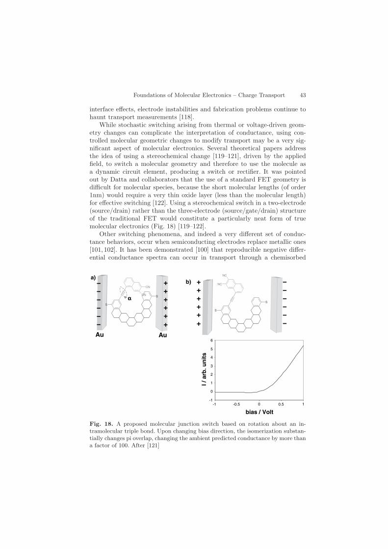
While stochastic switching arising from thermal or voltage-driven geom-etry changes can complicate the interpretation of conductance, using con-trolled molecular geometric changes to modify transport may be a very sig-nificant aspect of molecular electronics. Several theoretical papers addressthe idea of using a stereochemical change [119–121], driven by the appliedfield, to switch a molecular geometry and therefore to use the molecule asa dynamic circuit element, producing a switch or rectifier. It was pointedout by Datta and collaborators that the use of a standard FET geometry isdifficult for molecular species, because the short molecular lengths (of order1nm) would require a very thin oxide layer (less than the molecular length)for effective switching [122]. Using a stereochemical switch in a two-electrode(source/drain) rather than the three-electrode (source/gate/drain) structureof the traditional FET would constitute a particularly neat form of truemolecular electronics (Fig. 18) [119–122].
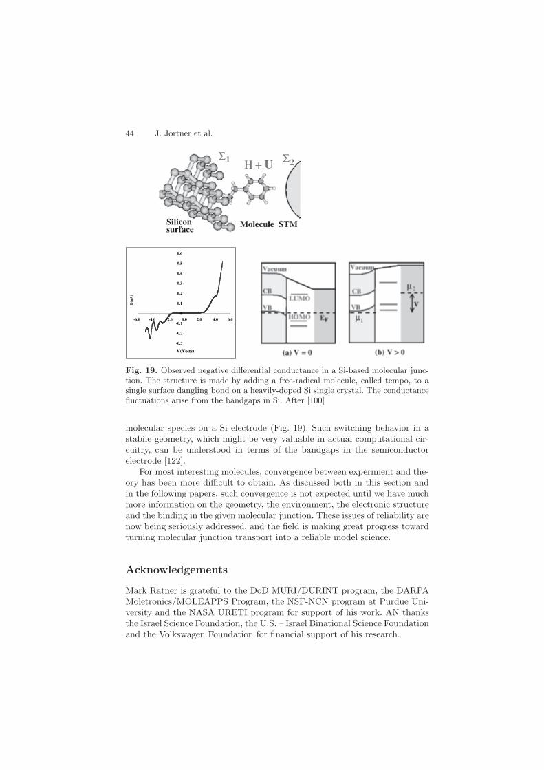
Other switching phenomena, and indeed a very different set of conduc-tance behaviors, occur when semiconducting electrodes replace metallic ones[101, 102]. It has been demonstrated [100] that reproducible negative differ-ential conductance spectra can occur in transport through a chemisorbed
-1 -0.5 0 0.5 1
bias / Volt
I / a
rb. u
nit
s
S
SCN
CN
NC
NC
S
S
− − − − − −
++ + + + +
αααα
Au
Au
++++++
− − − − − −
b)a)
-1
0
1
2
3
4
5
6
Fig. 18. A proposed molecular junction switch based on rotation about an in-tramolecular triple bond. Upon changing bias direction, the isomerization substan-tially changes pi overlap, changing the ambient predicted conductance by more thana factor of 100. After [121]
44 J. Jortner et al.
-0.3
-0.2
-0.1
0
0.1
0.2
0.3
0.4
0.5
0.6
-6.0 -4.0 -2.0 0.0 2.0 4.0 6.0
V(Volts)
I (n
A)
Fig. 19. Observed negative differential conductance in a Si-based molecular junc-tion. The structure is made by adding a free-radical molecule, called tempo, to asingle surface dangling bond on a heavily-doped Si single crystal. The conductancefluctuations arise from the bandgaps in Si. After [100]
molecular species on a Si electrode (Fig. 19). Such switching behavior in astabile geometry, which might be very valuable in actual computational cir-cuitry, can be understood in terms of the bandgaps in the semiconductorelectrode [122].
For most interesting molecules, convergence between experiment and the-ory has been more difficult to obtain. As discussed both in this section andin the following papers, such convergence is not expected until we have muchmore information on the geometry, the environment, the electronic structureand the binding in the given molecular junction. These issues of reliability arenow being seriously addressed, and the field is making great progress towardturning molecular junction transport into a reliable model science.
Acknowledgements
Mark Ratner is grateful to the DoD MURI/DURINT program, the DARPAMoletronics/MOLEAPPS Program, the NSF-NCN program at Purdue Uni-versity and the NASA URETI program for support of his work. AN thanksthe Israel Science Foundation, the U.S. – Israel Binational Science Foundationand the Volkswagen Foundation for financial support of his research.
Foundations of Molecular Electronics – Charge Transport 45
References
1. C. Joachim, J.K. Gimzewski, and A. Aviram: Electronics using hybrid-molecular and mono-molecular devices, Nature 408, 541 (2000).
2. A. Nitzan and M. Ratner: Electron transport in molecular wire junctions,Science 300, 1384 (2003).
3. A. Nitzan: Electron transmission through molecules and molecular interfaces,Ann. Rev. Phys. Chem. 52, 681 (2001).
4. P. Hanggi, M. Ratner, and S. Yaliraki, eds., Chemical Physics 281, 111 (2002).5. J.R. Heath and M.A. Ratner: Molecular electronics, Physics Today 56, 43
(2003); C.R. Kagan and M.A. Ratner, eds., MRS Bulletin, 29, #6 (2004)6. D.M. Adams, L. Brus, C.E.D. Chidsey, et al.: Charge transfer on the nanoscale:
Current status, J. Phys. Chem. B 107, 6668 (2003).7. M.C. Petty, M.R. Bryce, and D. Bloor, Introduction to Molecular Electron-
ics (Oxford University Press, Oxford, 1995); C.A. Mirkin, and M.A. Ratner:Molecular electronics, Annu. Rev. Phys. Chem., 43, 719 (1992); A. Aviram,ed., Molecular Electronics – Science and Technology (American Institute ofPhysics, College Park, MD, 1992); A. Aviram, M.A. Ratner, and V. Mu-jica: Molecular electronics – science and technology, eds., Ann. N.Y. Acad.Sci., 852, (1998); J. Jortner, and M.A. Ratner, eds. Molecular Electronics(Blackwell Science, Cambridge, MA, 1997); M.A. Ratner, and M.A. Reed,Encyclopedia of Science and Technology, 3rd ed., (Academic Press, New York,2002); V. Mujica, and M.A. Ratner, in Handbook of Nanoscience, Engineeringand Technology, W.A. Goddard III, D.W. Brenner, S.E. Lyshevshi, and G.J.Iafrate, eds. (CRC Press, Boca Raton, FL, 2002); M.A. Reed, and T. Lee, eds.,Molecular Nanoelectronics (American Scientific Publishers, Stevenson Ranch,CA, 2003).
8. Jeffrey R. Reimers, et al.: Molecular Electronics III, eds., Ann. N.Y. Acad.Sci., 1006, (2003).
9. Thomas Tsakalakos, Ilya A. Ovid’ko and Asuri K. Vasudevan, eds., Nanostruc-tures: Synthesis, Functional Properties and Applications, (Kluwer, Dordrecht,2003).
10. A. Aviram, M. Ratner, and V. Mujica, eds., Molecular electronics II, Ann.N.Y. Acad. Sci., 960, (2002).
11. J. Jortner, and M. Bixon, in Advances in Chemical Physics, I. Prigogine, and S.Rice, eds. 106 (Wiley, New York, 1999); A.M. Kuznetsov, Charge Transfer inPhysics, Chemistry and Biology (Gordon & Breach, New York, 1995); A.M.Kuznetsov, J. Ulstrup, A.M.K., et al., Electron Transfer in Chemistry andBiology: An Introduction to the Theory (Wiley, New York, 1998).
12. R.A. Marcus: Chemical and electrochemical electron-transfer theory, Ann.Rev. Phys. Chem. 15, 155 (1964).
13. J.R. Miller, J.V. Beitz, and R. Huddleston: Effect of free energy on rates ofelectron transfer between molecules, J. Am. Chem. Soc. 106, 5057 (1984).
14. J. Jortner and B. Pullman, eds., Perspectives in Photosynthesis. Dordrecht:Kluwer, 1990.
15. J. Jortner, M. Bixon, T. Langenbacher, and M.E. Michel-Beyerle: Chargetransfer and transport in DNA, Proceed. Natl. Acad. Sci. USA 95, 12759(1998).
16. M. Bixon and J. Jortner, [1], p. 35.
46 J. Jortner et al.
17. J. Ulstrup and J. Jortner: The effect of intramolecular quantum modes on freeenergy relationships for electron transfer reaction, J. Chem. Phys. 63, 4358(1975).
18. M. Bixon and J. Jortner: Solvent relaxation dynamics and electron transfer,Chem. Phys. 176, 467 (1993).
19. T. Holstein: Polaron motion. I. Molecular crystal model, Ann. Phys. (N.Y.)8, 325, 343 (1959).
20. H. McConnell: Intramolecular charge transfer in aromatic free radicals, J.Chem. Phys. 35, 508 (1961).
21. J. Jortner: Temperature dependent activation energy for electron transfer be-tween biological molecules, J. Chem. Phys. 64, 4860 (1976); V. Mujca, M.Kemp, M. Roitberg, and M.A. Ratner: Electron conduction in molecularwires. I. A scattering formalism and II. Application to scanning tunnelingmicroscopy, J. Chem. Phys. 101, 6849, 6856 (1994).
22. J. Tersoff, and D.R. Hamann: Theory of the scanning tunneling microscope,Phys. Rev. B, 31, 805 (1985).
23. R. Landauer: Spatial variation of currents and field due to localized scatterersin metallic conduction, IBM J. Res. Dev. 1, 223, (1957); R. Landauer: Elec-trical resistance of disordered one-dimensional lattices, Phil. Mag., 21, 863(1970).
24. C.W.J. Beenakker, and H. van Houten: Advances in research and applications.Qantum transport in semiconductor nanostructures, Solid State Physics, 44,1 (Academic Press, New York, 1991).
25. L.V. Keldysh, Sov. Phys. JETP, 20, 1018 (1965).26. L. P. Kadanoff, and G. Baym, Quantum Statistical Mechanics; Green’s func-
tion Methods in Equilibrium and Nonequilibrium (W.A. Benjamin, New York,1962).
27. Y. Meir and N.S. Wingreen: Landauer formula for the current through aninteracting electron region, Phys. Rev. Lett. 68, 2512 (1992)
28. T. Seideman, and W.H. Miller: Quantum mechanical reaction probabilitiesvia a discrete variable representation-absorbing boundary condition Green’sfunction, J. Chem. Phys., 97, 2499 (1992); T. Seideman, and W.H. Miller:Calculation of the cumulative reaction probability via a discrete variable rep-resentation with absorbing boundary conditions, J. Chem. Phys, 96, 4412(1992).
29. S. Datta, Electric transport in Mesoscopic Systems (Cambridge UniversityPress, Cambridge, 1995); S. Datta, to be published.
30. Y. Xue, S. Datta, and M.A. Ratner: Charge transfer and “band lineup”in molecular electronic devices: A chemical and numerical interpretation, J.Chem. Phys., 115, 4292 (2001).
31. L.E. Hall, J.R. Reimers, N.S. Hush, et al.: Formalism, analytical model, anda priori Green’s-function-based calculations of the current-voltage character-istics of molecular wires, J. Chem. Phys., 112, 1510 (2000).
32. S. Datta, W.D. Tian, S.H. Hong, et al.: Current-voltage characteristics of self-assembled monolayers by scanning tunneling microscopy, Phys. Rev. Lett., 79,2530 (1997).
33. H. Ness, and A.J. Fisher: Quantum inelastic conductance through molecularwires, Phys. Rev. Lett., 83, 452 (1999); E.G. Petrov, I.S. Tolokh, and V. May:The magnetic-field influence on the inelastic electron tunnel current mediated
Foundations of Molecular Electronics – Charge Transport 47
by a molecular wire, J. Chem. Phys., 109, 9561 (1998); E.G. Emberly, and G.Kirczenow: Electron standing-wave formation in atomic wires, Phys. Rev. B,60, 6028 (1999); E.G. Emberly, and G. Kirczenow: Models of electron trans-port through organic molecular monolayers self-assembled on nanoscale metal-lic contacts, Phys. Rev. B, 64, 235412 (2001); M. Brandbyge et al.: Density-functional method for nonequilibrium electron transport, Phys. Rev. B, 65,165401 (2002); B. Larade, et al.: Conductance, I-V curves, and negative dif-ferential resistance of carbon atomic wires, Phys. Rev. B, 64, 075420 (2001); J.Taylor, H. Guo, J. Wang: Ab initio modeling of open systems: Charge transfer,electron conduction, and molecular switching of a C60 device, Phys. Rev. B,63, 121104(R) (2001); M. Magoga, and C. Joachim: Minimal attenuation fortunneling through a molecular wire, Phys. Rev. B, 57, 1820 (1998); M. Ma-goga, and C. Joachim: Conductance of molecular wires connected or bondedin parallel, Phys. Rev. B, 59, 16011 (1999); P. Stampfus, et al., in ProceedingsNIC Symposium; D. Wolf, G. Munster, M. Kremer, eds., 20, 101 (2003); R.Baer and D. Neuhauser: Ab initio electrical conductance of a molecular wire,Int. J. Quant. Chem., 91, 524 (2003); R. Baer, et al: Ab initio study of thealternating current impedance of a molecular junction, J. Chem. Phys. 120,3387 (2004).
34. J.K. Tomfohr, and O. Sankey: Complex band structure, decay lengthg, andFermi level alignment in simple molecular electronic systems, Phys. Rev. B,65, 245105 ( 2002); B. Larade, J. Taylor, H. Mehrez, and H. Guo: Conduc-tance, I-V curves, and negative differential resistance of carbon atomic wires,Phys Rev. B, 64, 075420 (2001); J. Taylor, H. Guo, and J. Wang: Ab initiomodeling of open systems; Charge transfer, electron conduction, and molecu-lar switching of a C60 device, Phys. Rev. B, 63, 121104(R) (2001); H. Mehrez,G. Hong, J. Wang, and C. Roland: Carbon nanotubes in the Coulomb block-ade regime, Phys. Rev. B, 63, 245410/1 (2001); A. di Carlo et al.: Theoreticaltools for transport in molecular nanostructures, Physica B, 314, 86 (2002);J.C. Cuevas et al.: theoretical description of the electrical conduction in atomicand molecular junctions, Nanotechnology, 14, R29 (2003); J.J. Palacios et al.:First-principal approach to electrical transport in atomic-scale nanostructures,Phys. Rev. B, 66, 035322 (2002).
35. Y.Q. Xue and M.A. Ratner: Microscopic study of electrical transport throughindividual molecules with metallic contacts. (2). Effect fo the interface struc-ture, Phys. Rev. B, 68, 115407 (2003); and: Schottky barrier at metal-finitesemiconduction carbon nanotube interfaces, Appl. Phys. Lett. 83, 2429 (2003).
36. T. Seideman, and H. Guo: Quantum transport and current-triggered dynamicsin molecular tunnel junctions, J. Theor. Comp. Chem., 2, 439 (2004).
37. N.D. Lang: Resistance of atomic wires, Phys. Rev. B, 52, 5335 (1995).38. N.D. Lang, and P. Avouris: Carbon-atom wires: Charge-transfer doping, volt-
age drop, and the effect of distortions, Phys. Rev. Lett., 84, 358 (2000).39. M. diVentra, S. Pantelides, and N. Lang: Erratum: Current-induced forces
in molecular wires [Phys. Rev. Lett., 88, 046801 (2002)], Phys. Rev. Lett.,89, 139902 (2002); M. Di Ventra, and S.T. Pantelides: Scanning tunnelingmicroscopy images: A full ab initio approach, Phys. Rev. B, 59, R5320 (1999).
40. S.N. Rashkeev, M. Di Ventra, and S.T. Pantelides: Transport in moleculartransistors: Symmetry effects and nonlinearities, Phys. Rev. B, 66, 033301/1(2002); Y. Zhongqin, N.D. Lang, and M. Di Ventra: Effects of geometry and
48 J. Jortner et al.
doping on the operation of molecular transistors, App. Phys. Lett., 82, 1938(2003); S.T. Pantelides, M. Di Ventra, and N.D. Lang: First-principles simu-lations of molecular electronics, Ann. N.Y. Acad. Sci., 960, 177 (2002); S.T.Pantelides, M. Di Ventra, N.D. Lang, and S.N. Rashkeev: Molecular electron-ics by the numbers, IEEE Transactions on Nanotechnology, 1, 86 (2002); M.Di Ventra, N.D. Lang, and S.T. Pantelides: Electronic transport in single mole-cules, Chem. Phys., 281, 189 (2002); M. Di Ventra, S.T. Pantelides, and N.D.Lang: Current-induced forces in molecular wires, Phys. Rev. Lett., 88, 046801(2002); M. Di Ventra, and N.D. Lang: Transport in nanoscale conductors fromfirst principles, Phys. Rev. B, 65, 045402 (2002).
41. A. Troisi, and M.A. Ratner: Molecular wires conductance: Some theoreticaland computational aspects, Molecular Nanoelectronics, M.A. Reed, and T.Lee, eds., 1 (American Scientific Publishers, Stevenson Ranch, CA, 2003).
42. R.H.M. Smit, Y. Noat, C. Untiedt, N.D. Lang, M.C.V. Hemert, and J.M. vanRuitenbeek: Measurement of the conductance of a hydrogen molecule, Nature,419, 906 (2002).
43. M. Fuhrer, S.A. Getty, L. Wang, C. Engtrakul, and L. R. Sita: Near-perfectconduction through a ferrocene-based molecular wire, unpublished.
44. A. Nitzan: A relationship between electron-transfer rates and molecular con-duction, J. Phys. Chem. A, 105, 2677 (2001).
45. A. Nitzan: The relationship between electron-transfer rate and molecular con-duction. (2). The sequential hopping case, Israel J. Chem., 42, 163 (2002).
46. R.A. Marcus: On the theory of electron-transfer reactions. (6). Unified treat-ment for homogeneous and electrode reactions, J. Chem. Phys., 43, 679(1965); M.D. Newton: Quantum chemical probes of electron-transfer kinet-ics: The nature of donor acceptor interactions, Chem. Rev., 91, 767 (1991).
47. D.M. Adams et al.: Charge transfer on the nanoscale: Current status, J. Phys.Chem. B, 107, 6668 (2003)
48. J. Park, A.N. Pasupathy, J.I. Goldsmith, C.C. Chang, Y. Yaish, J.R. Petta, M.Rinkoski, J.P. Sethna, H.D. Abruna, P.L. McEuen, and D.C. Ralph: Coulombblockade and the Kondo effect in single-atom transistors, Nature, 417, 722(2002); W. Liang et al.: Kondo resonance in a single-molecule transistor, Na-ture 417, 725 (2002)
49. S. Kubatkin, A. Danilov, M. Hjort, J. Cornil, J.-L. Bredas, N. Stuhr-Hansen,P. Hedegard, and T. Bjornholm: Single-electron transistor of a single organicmolecule with access to several redox states, Nature, 425, 698 (2003).
50. D. Segal and A. Nitzan: Steady-state quantum mechanics of thermally relaxingsystems, Chem. Phys. 268, 315 (2001); D. Segal, and A. Nitzan: Heating incurrent carrying molecular junctions, J. Chem. Phys., 117, 3915 (2002).
51. D. Segal, A. Nitzan, and P. Hanggi: Thermal conductance through molecularwires, J. Chem. Phys., 119, 6840 (2003).
52. Y.-C. Chen, M. Zwolak, and M. DiVentra: Local heating in nanoscale con-ductors, Nano Lett., 3, 1691 (2003); T.N. Todorov: Local heating in ballis-tic atomic-scale contacts, Philosoph. Mag. B, 77(4), 965 (1998); M.J. Mont-gomery, T.N. Todorov, and A.P. Sutton: Power dissipation in nanoscale con-ductors, J. Phys.: Cond. Matt., 14, 5377 (2002).
53. B.C. Stipe, M.A. Rezaei, and W. Ho: Inducing and viewing the rotationalmotion of a single molecule, Science, 279, 1907 (1998).
Foundations of Molecular Electronics – Charge Transport 49
54. B.C. Stipe, M.A. Rezaei, and W. Ho: Localiztion of inelastic tunneling andthe determination of atomic-scale structure with chemical specifity, Phys. Rev.Lett., 82, 1724 (1999).
55. T. Komeda, Y. Kim, M. Kawai, B.N.J. Persson, and H. Ueba: Lateral hoppingof molecules induced by excitation of internal vibration mode, Science, 295,2055 (2002).
56. S. Alavi, B. Larade, J. Taylor, H. Guo, and T. Seideman: Current-triggeredvibrational excitation in single-molecule transistors, Chem. Phys., 281, 293(2002); T. Seideman: Current-triggered dynamics in molecular-scale devices,J. Phys.: Cond. Matt., 15, R521 (2003); B.N.J. Persson, and H. Ueba; Theoryof inelastic tunneling induced motion of adsorbates on metal surfaces, Surf.Sci., 12, 502 (2002).
57. S.-W. Hla, L. Bartels, G. Meyer, and K.-H. Rieder: Inducing all steps of achemical reaction with the scanning tunneling microscope tip: Towards singlemolecule engineering, Phys. Rev. Lett., 85, 2777 (2000); G.V. Nazin, X.H. Qiu,and W. Ho: Visualization and spectroscopy of a metal-molecule-metal bridge,Science, 302, 77 (2003); J.R. Hahn, and W. Ho: Oxidation of a single car-bon monoxide molecule manipulated and induced with a scanning tunnelingmicroscope, Phys. Rev. Lett., 87, 166102 (2001).
58. E.L. Wolf, Principles of electron tunneling spectroscopy (Oxford UniversityPress, New York, 1985); K.W. Hipps and U. Mazur: Inelastic electron tunnel-ing: An alternative molecular spectroscopy, J. Phys. Chem., 97, 7803 (1993).
59. H.J. Lee and W. Ho: Single-bond formation and characterization with a scan-ning tunneling microscope, Science, 286, 1719 (1999); N. Lorente, M. Persson,L.J. Lauhon, and W. Ho: Symmetry selection rules for vibrationally inelastictunneling, Phys. Rev. Lett., 86, 2593 (2001); J.R. Hahn, and W. Ho: Singlemolecule imaging and vibrational spectroscopy with a chemical modified tipof a scanning tunneling microscope, Phys. Rev. Lett., 87, 196102 (2001); L.J.Lauhon and W. Ho: Direct observation of the quantum tunneling of singlehydrogen atoms with a scanning tunneling microscope, Phys. Rev. Lett., 85,4566 (2000); J. Gaudioso, J.L. Laudon, and W. Ho: Vibrationally mediatednegative differential resistance in a single molecule, Phys. Rev. Lett., 85, 1918(2000); L.J. Lauhon and W. Ho: Single-electron vibrational spectroscopy andmicroscopy: CO on Cu(001) and Cu(110), Phys. Rev. B, 60, R8525 (1999);H.J. Lee and W. Ho: Structural determination by single-molecule vibrationalspectroscopy and microscopy: Contrast between copper and iron carbonyls,Phys. Rev. B, 61, R16347 (2000).
60. J.R. Hahn, H.J. Lee, and W. Ho: Electronic resonance and symmetry in single-molecule inelastic electron tunneling, Phys. Rev. Lett., 85, 1914 (2000).
61. N.B. Zhitenev, H. Meng, and Z. Bao: Conductance of small molecular junc-tions, Phys. Rev. Lett., 88, 226801 (2002); H. Park, J. Park, A.K.L. Lim, E.H.Anderson, A.P. Alivisatos, and P.L. McEuen: Nanomechanical oscillations ina single-C60 transistor, Nature, 407, 57 (2000).
62. W. Wang, T. Lee, I. Kretzschmar, and M.A. Reed: Inelastic electron tunnelingspectroscopy of alkanedithiol self-assembled monolayers, Nano Lett., 4, 643(2004); J.G. Kushmerick, J. Lazorcik, C.H. Patterson, R. Shashidhar, D.S.Seferos, and G.C. Bazan: Vibronic contributions to charge transport acrossmolecular junctions, Nano Lett., 4, 639 (2004).
50 J. Jortner et al.
63. A. Nitzan, M. Galperin, and M.A. Ratner: Inelastic electron tunneling spec-troscopy in molecular junctions: Peaks and dips, submitted for publication(cond-mat/0405472).
64. A. Nitzan, J. Jortner, J. Wilkie, et al.: Tunneling time for electron transferreactions, J. Phys. Chem. B, 104, 5661-5665 (2000).
65. U. Peskin, A. Edlund, I. Bar-On, et al.: Transient resonance structures inelectron tunneling through water, J. Chem. Phys., 111, 7558 (1999).
66. E. Yablonovitch: The chemistry of solid-state electronics, Science, 246, 347(1989).
67. R. Venugopal, M. Paulsson, S. Goasguen, S. Datta, and M. Lundstrom: Asimple quantum mechanical treatment of scattering in nanoscale transistors,J. App. Phys., 93, 5613 (2003); M. Buttiker: Four-terminal phase-coherentconductance, Phys. Rev. Lett., 57, 1761 (1986).
68. M. Bixon, and J. Jortner: Vibrational coherence in nonadiabatical dynamics,J. Chem. Phys., 107, 1470 (1997).
69. M. Bixon, and J. Jortner: Electron transfer via bridges, J. Chem. Phys., 107,5154 (1997).
70. Y. Selzer, et al.: Temperature effects on conduction through a molecular junc-tion, Nanotechnology 15, S483 (2004); and: Thermally activated conductionin molecular junctions, J. Am. Chem. Soc. 126, 4052 (2004).
71. B. Giese et al.: Direct observation of the hole transfer through DNA by hop-ping between adenine beaes and by tunneling, Nature 412, 318 (2001).
72. D. Segal, A. Nitzan, W.B. Davis, M.R. Wasilewski, and M.A. Ratner: Elec-tron transfer rates in bridged molecular systems. 2. A steady-state analysisof coherent tunneling and thermal transitions, J. Phys. Chem. B, 104, 3817(2000); D. Segal, and A. Nitzan: Conduction in molecular junctions: Inelasticeffects, Chem. Phys., 281, 235 (2002); D. Segal, and A. Nitzan: Steady-statequantum mechanics of thermally relaxing systems, Chem. Phys., 268, 315(2001), and references therein.
73. D. Segal, and A. Nitzan: Heating in current carrying molecular junctions, J.Chem. Phys., 117, 3915 (2002).
74. X.H. Qiu, G.V. Nazin, and W. Ho: Vibronic states in single molecule electrontransport, Phys. Rev. Lett., 92, 206102 (2004).
75. B.N.J. Persson, and A. Baratoff: Inelastic electron tunneling from a metal tip:The contribution from resonant processes, Phys. Rev. Lett., 59, 339 (1987).
76. A. Bayman, P. Hansma, and W.C. Kaska: Shifts and dips in inelastic-electron-tunneling spectra due to the tunnel-junction environment, Phys. Rev. B, 24,2449 (1981).
77. M. Galperin, M.A. Ratner, and A. Nitzan: Hysteresis, switching and negativedifferential reistance in molecular junctions: A polaron model, Nano Letters,5(1), 125 (2005).
78. M.R. Wasielewski: Photoinduced electron transfer in supramolecular systemsfor artificial photosynthesis, Chem. Rev., 92, 435 (1992).
79. G. Closs, J.R. Miller: Intramolecular long-distance electron transfer in organicmolecules, Science, 240, 440 (1988).
80. J. Lehmann, S. Kohler, P. Hanggi, and A. Nitzan: Molecular wires acting ascoherent quantum ratchets, Phys. Rev. Lett., 88, 228305 (2002); J. Lehmann,S. Kohler, P. Hanggi, and A. Nitzan: Rectification of laser-induced eletronictransport through molecules, J. Chem. Phys., 118, 3283 (2002); S. Kohler,
Foundations of Molecular Electronics – Charge Transport 51
S. Camalet, M. Strass, J. Lehmann, G.-L. Ingold, and P. Hanggi: Chargetransport through a molecule driven by a high-frequency field, Chem. Phys.,296, 243 (2004); J. Lehmann, S. Camalet, S. Kohler, and P. Hanggi: Lasercontrolled molecular switches and transistors, Chem. Phys. Lett., 368, 282(2003); A. Keller, O. Atabek, M. Ratner, and V. Mujica: Laser-assisted con-ductance of molecular wires, J. Phys. B Atomic Molecular & Optical Physics,35, 4981 (2002); A. Tikhonov, R.D. Coalson, and Y. Dahnovsky: Calculatingelectron transport in a tight-binding model of a field driven molecular wire:Floquet theory, J. Chem. Phys., 116, 10909 (2002); A. Tikhonov, R.D. Coal-son, and Y. Dahnovsky: Calculating electron current in a tight-binding modelof a field driven molecular wire: Application to xylyl-dithiol, J. Chem. Phys.,117, 567 (2002).
81. Y. Kamada, N. Naka, S. Saito, N. Nagasawa, Z.M. Li, and Z.K. Tang: Photo-irradiation effects on electrical conduction of single wall carbon nanotubes,Solid State Communications, 123, 375 (2002); V. Gerstner, A. Knoll, W.Pfeiffer, A. Thon, and G. Gerber: Femtosecond laser assisted scanning tun-neling microscopy, J. Appl. Phys., 88, 4851 (2000); R.J. Schoelkopf, A.A.Kozhevnikov, D.E. Prober, and M.J. Rooks: Observation of “photon-assisted”shot-noise in a phase-coherent conductor, Phys. Rev. Lett., 80, 2437 (1998);R.J. Schoelkopf, P.J.B. , A.A. Kozhevnikov, D.E. Prober, and M.J. Rooks: Fre-quency dependence of shot noise in a diffusive mesoscopic conductor, Phys.Rev. Lett., 78, 3370 (1997); B.J. Keay, S.J. Allen, Jr., J. Galan, J.P. Kamin-ski, K.L. Campman, A.C. Gossard, U. Bhattacharya, and M.J.W. Rodwell:Photon-assisted electric field domains and multiphoton-assisted tunneling insemiconductor superlattices, Phys. Rev. Lett., 75, 4098 (1995); Dulic D, et al.:One-way optoelectronic switching of photochromic molecules on gold, Phys.Rev. Lett., 91, 207402 (2003).
82. T. Frauenheim, et al.: Atomistic simulations of complex materials: Groundstate and excited-state properties, J. Phys. Cond. Matt., 14, 3015 (2002).
83. C.W. Bauschlicher, Jr., A. Ricca, Y. Xue, and M.A. Ratner: Current-voltagecurves for molecular junctions: pyrene versus diphenylacetylene, Chem. Phys.Lett., 390, 246 (2004); J.M. Seminario, L.E. Cordova and P.A. Derosa: Anab initio approach to the calculation of current-voltage characteristics of pro-grammable molecular devices, Proc. IEEE 91, 1958 (2000); Y. Xue, S. Datta,and M.A. Ratner: Charge transfer and “band lineup” in molecular electronicdevices: A chemical and numerical interpretation, J. Chem. Phys., 115, 4292( 2001).
84. K. Tagami, L. Wang, and M. Tsukada: Interface sensitivity in quantum trans-port through single molecules, Nano Lett., 4, 209 (2004); E. Emberly and G.Kirczenow: Molecular spintronics: Spin-dependent electron transport in mole-cular wires, Chem. Phys. 281, 311(2002); E.G Petrov, I.S. Tolokh and V. May:Magnetic field control of an electron tunnel current through a molecular wire,J. Chem. Phys. 108, 4386(1998).
85. Z.Q. Yang and M. Di Ventra: Nonlinear current-induced forces in Si atomicwires, Phys. Rev. B 67, 161311 (2003).
86. X.-Y. Zhu: Charge transport at metal-molecule interfaces: A spectroscopicview, J. Phys. Chem. B, 108, (2004).
87. S. Datta, W. Tian, S. Hong, R. Reifenberger, J.I. Henderson, C.P. Kubiak:Current-voltage characteristics of self-assembled monolayers by scanning tun-
52 J. Jortner et al.
nelling microscopy, Phys. Rev. Lett., 79, 2530 (1997); W. Tian, S. Datta, S.Hong, R. Reifenberger, J.I. Henderson, and C.P. Kubiak: Conductance spec-tra of molecular wires, J. Chem. Phys., 109, 2874 (1998); Y. Xue, S. Datta, S.Hong, R. Reifenberger, J.I. Henderson, and C.P. Kubiak: Negative differentialresistance in the scanning tunneling spectroscopy of organic molecules, Phys.Rev. B, 59, R7852 (1999).
88. V. Mujica, A.E. Roitberg and M. Ratner: Molecular wire conductance: Eloc-trostatic potential spatial profile, J. Chem. Phys. 112, 6834 (2000)
89. A. Xue, and M.A. Ratner: Microscopic study of electrical transport throughindividual molecules with metallic contacts. II. Effect of the interface struc-ture, Phys. Rev. B, 68, 115407 (2003).
90. C. Liang, A.W. Ghosh, M. Paulsson, S. Datta: Electrostatic potential profilesof molecular conductors, Phys. Rev. B, 69, 115302 (2004).
91. M. Di Ventra, S.T. Pantelides, and N.D. Lang: The benzene molecule as amolecular resonant-tunneling transistor, App. Phys. Lett., 76, 3448 (2000).
92. A. Bachtold, et al.: Scanned probe microscopy of electronic transport in carbonnanotubes, Phys. Rev. Lett., 84, 6082 (2000).
93. Y. Karzazi, et al.: Influence of contact geometry and molecular derivatizationon the interfacial interactions between gold and conjugated wires, Chem. Phys.Lett., 387, 502 (2004); H. Basch, and M.A. Ratner: Binding at molecule/goldtransport interfaces. II. Orbitals and density of states, J. Chem. Phys., 119,11943 (2003).
94. F. Zahid, M. Paulsson and S. Datta: Electrical conduction through molecules,in Advanced Semiconductors and Organic Nanotechniques, H. Morkoc, ed.,(Academic Press, New York, 2003).
95. F. Zahid, M. Paulsson et al., to be published.96. A. Rassolov, M.A. Ratner, and J.A. Pople: Semiempirical models for image
eletrostatics. I. Bare external charge, J. Chem. Phys., 114, 2062 (2001).97. V. Mujica, M. Kemp, and M.A. Ratner: Electron conduction in molecular
wires. I. A scattering formalism and II. Application to scanning tunnelingmicroscopy, J. Chem. Phys., 101, 6849, 6856 (1994).
98. D.S. Kosov: Schrodinger equation for current carrying states, J. Chem. Phys.,116, 6368 (2002); J. Tomfohr, O. F. Sankey: Theoretical analysis of electrontransport through organic molecules, J. Chem. Phys., 120, 1542 (2004); K.Thygesen et al., work in progress; R. Car, K. Burke, et al, work in progress.
99. J. Reichert, H.B. Weber, M. Mayor, H.V. Lohneysen: Low-temperature con-ductance measurements on single molecules, Appl. Phys. Lett., 82, 4137(2003); J.O. Lee et al.: Electrical transport study of phenylene-based π-conjugated molecules in a three terminal geometry, Annals Of The New YorkAcademy Of Sciences, 1006, 122 (2003); D. Janes et al., to be published; M.A.Reed, et al.: Conductance of a molecular junction, Science, 278, 252 (1997).The structure assumed here may be incorrect: e.g. P.L. Pugmire, M.J. Tarlov,R.D. van Zee: The structure of benzenedimethanethiol self-assembled mono-layers on gold grown by solution and vapor techniques, Langmuir, 19, 3720(2003).
100. N.P. Guisinger, M.E. Greene, R. Basu, A.S. Baluch, M.C. Hersam: Room tem-perature negative differential resistance through individual organic moleculeson silicon surfaces, Nano Lett., 4, 55 (2004).
Foundations of Molecular Electronics – Charge Transport 53
101. X.P. Cao, R.J. Hamers: Silicon surfaces as electron acceptors: Dative boundingof amines with Si(001) and Si(111) surfaces, J. Am Chem Soc 123, 10988(2001); S.N. Patitsas et al.: Current-induced organic-silicon bond breaking:Consequences for molecular devices, Surf. Sci. 457, L425 (2000)
102. J.G. Kushmerick, et al.: Understanding charge transport in molecular elec-tronics, Ann. NY Acad. Sci. 1006, 277 (2003)
103. X.D. Cui, et al.: Reproducible measurement of single-molecule conductivity,Science, 294, 571(2001).
104. B. Mantooth, et al.: Cross-correlation image tracking for adsorbate analysisand drift correction, Rev. Sci. Inst., 73, 313 (2002).
105. R.P. Andres, et al.: “Coulomb staircase” at room temperature in a self-assembled molecular nanostructure, Science 272, 1323 (1996); A. Dhirani, etal.: Self-assembled molecular rectifiers, J. Chem. Phys. 106, 5249 (1997); R.McCreery, et al.: Molecular rectification and conductance swithing in carbon-based molecular junctions by structural rearrangement accompanying electroninjection, J. Am. Chem. Soc. 125, 10748 (2003); D.J. Wold, et al.: Distancedependence of electron tunneling through aelf-assembled monolayers measuredby conducting probe atomic force microscopy: Unsaturated versus saturatedmolecular junctions, J. Phys. Chem. B, 106, 2813 (2002)
106. C. Lin, and C.R. Kagan: Layer-by-layer growth of metal-metal bondedsupramolecular thin films and its use in the fabrication of lateral nanoscaledevices, J. Am. Chem. Soc., 125, 336 (2003).
107. Y. Selzer, et al.: Temperature effects on conduction through a molecular junc-tion, Nanotechnology, 15, S483 (2004).
108. H. Basch, and M.A. Ratner, unpublished.109. G. Poirier: Characterization of organosulfur molecular monolayers on Au(111)
using scanning tunneling microscopy, Chem. Revs., 97, 1117 (1997).110. S. Liu, R. Maoz, J. Sagiv: Planned nanostructures of colloidal gold via self-
assemply on hierarchically assembled organic bilayer template patterns within-situ generated terminal amino functionality, Nano Lett., 4, 845 (2004).
111. X.Y. Xiao, B.Q. Xu, N.J. Tao: Measurement of single molecule conductance:Benzenedithiol and benzenedimethanethiol; Nano Lett., 4, 267 (2004).
112. W. Wang, T. Lee, and M.A. Reed: Mechanism of electron conduction in self-assembled alkanethiol monolayer devices, Phys. Rev. B, 68, 035416 (2003).
113. J.W. Gadzuk and E.W. Plummer: Field emission energy distribution (FEED),Revs. Mod. Phys., 45, 487 (1973).
114. G.G. Fagas, A. Kambili and M. Elstner: Complex band structure: A method todetermine the off-resonant electron transport in oligomers, Chem. Phys. Lett.,389, 268 ( 2004); V. Mujica, and M.A. Ratner: Current-voltage characteristicsof tunneling molecular junctions for off-resonance injection, Chem. Phys., 264,395 (2002).
115. W. Wang, T. Lee, and M.A. Reed: Intrinsic molecular electronic transport:Mechanisms and mehtods, J. Phys. Chem. B, in press.
116. C.C. Kaun, H. Guo: Resistance of alkanethiol molecular wires, Nano Lett., 3,1521 (2003).
117. H. Basch, and M.A. Ratner: Binding at molecule/gold transport interfaces. V.Comparison of different metals and molecular bridges, submitted to J. Chem.Phys.
118. A. Salomon, et al.: Comparison of electronic transport measurements on or-ganic molecules, Adv. Mat. 15, 1881 (2003)
54 J. Jortner et al.
119. P.E. Kornilovitch, A.M. Bratkovsky, and R. S. Williams: Bistable molecularconductors with a field-switchable dipole group, Phys. Rev. B, 66, 245413(2002).
120. E.G. Emberly, and G. Kirczenow: The smallest molecular switch, Phys. Rev.Lett., 91, 188301 (2003).
121. A. Troisi, M.A. Ratner: Conformational molecular rectifiers, Nano Lett., 4,591 (2004).
122. T. Rakshit, G.C. Liang, A. Ghosh, S. Datta: Silicon based molecular electron-ics, cond-mat/0305695 (2003), submitted to Phys. Rev. Lett.