Embed Size (px)
Citation preview

UNIVERSIDAD DE LA REPUBLICA
Facultad de Ingenierıa
Instituto de Ingenierıa Electrica
Tesis para optar por el Tıtulode Magister en Ingenierıa Electrica
Modular Architecture For Ultra LowPower Switched-Capacitor DC-DC
Converters
Author:Ing.Pablo Castro Lisboa
Academic Director:Prof.Fernando Silveira
Thesis Advisors:Prof.Fernando SilveiraProf.Adj.Gabriel Eirea
Montevideo, Uruguay
22 de febrero de 2012

II

UNIVERSIDAD DE LA REPUBLICA ORIENTAL DELURUGUAY
FACULTAD DE INGENIERIA
INSTITUTO DE INGENIERIA ELECTRICA
Los abajo firmantes certificamos que hemos leıdo el presente trabajo titulado“Mo-dular Architecture For Ultra Low Power Switched Capacitor DC-DC Converters”hecho porPablo Castroy encontramos que el mismo satisface los requerimientos cu-rriculares que la Facultad de Ingenierıa exige para la tesis del tıtulo de Magister enIngenierıa Electrica.
Fecha: 9 de Diciembre de 2011
Director academico y Co-tutor de tesis:
Prof.Fernando Silveira:
Co-Tutor de Tesis:
Prof.Adj.Gabriel Eirea:
Tribunal Examinador:
Prof.Jose Luis Huertas:
Prof.Cesar Briozzo:
Prof.Agr.Conrado Rossi:
III

IV

A mis padres....Que me dieron lo mas importante.
V

Reconocimientos
A mis tutores Fernando Silveira y Gabriel Eirea por haberme dado la oportunidadde llevar adelante este trabajo, y por su permanente disponibilidad para guiarme lo cualvaloro mucho.
A la ANII (Agencia Nacional de Investigacion e Innovacion) por la beca otorgada.
Al cluster de Facultad de Ingenierıa de la UDELAR por haberme permitido hacerla exploracion del espacio de diseno.
VI

Contents
1. Introduction 11.1. Motivation. . . . . . . . . . . . . . . . . . . . . . . . . . . . . . . . 11.2. General Considerations forSwitched Capacitor Converters . . . . 4
1.2.1. Losses InSwitched Capacitor Converters . . . . . . . . . . 61.2.2. Efficiency. . . . . . . . . . . . . . . . . . . . . . . . . . . . 71.2.3. Output Resistance. . . . . . . . . . . . . . . . . . . . . . . 8
2. Proposed Architecture 112.1. Capacitors Implementation. . . . . . . . . . . . . . . . . . . . . . . 132.2. Charge Transfer Analysis. . . . . . . . . . . . . . . . . . . . . . . . 142.3. Parasitic Capacitances Losses. . . . . . . . . . . . . . . . . . . . . . 182.4. Rotation Technique to Reduce Parasitic Capacitances Losses. . . . . 222.5. Energy Saved with Improved Rotation Technique. . . . . . . . . . . 272.6. The Control Logic. . . . . . . . . . . . . . . . . . . . . . . . . . . . 292.7. Chapter Summary. . . . . . . . . . . . . . . . . . . . . . . . . . . . 30
3. Numerical Model 333.1. General Considerations for the Model. . . . . . . . . . . . . . . . . 33
3.1.1. Non-linear Capacitors. . . . . . . . . . . . . . . . . . . . . 343.1.2. Switches Resistances. . . . . . . . . . . . . . . . . . . . . . 343.1.3. Representation in the State Space. . . . . . . . . . . . . . . 34
3.2. Phase T1. . . . . . . . . . . . . . . . . . . . . . . . . . . . . . . . . 373.3. Phase T2. . . . . . . . . . . . . . . . . . . . . . . . . . . . . . . . . 383.4. Energy Losses. . . . . . . . . . . . . . . . . . . . . . . . . . . . . . 40
3.4.1. Parasitic Capacitances Losses. . . . . . . . . . . . . . . . . 403.4.2. Gate-drive Losses. . . . . . . . . . . . . . . . . . . . . . . . 403.4.3. Conduction Losses. . . . . . . . . . . . . . . . . . . . . . . 413.4.4. Digital and Analog Control Circuits Losses. . . . . . . . . . 41
3.5. How the Model Works . . . . . . . . . . . . . . . . . . . . . . . . . 413.5.1. Magnitudes That Change With Each Time Step. . . . . . . . 423.5.2. Magnitudes That Change With Events. . . . . . . . . . . . . 423.5.3. Model Pseudo Code. . . . . . . . . . . . . . . . . . . . . . 43
VII

3.6. Comparison with Electrical Simulations. . . . . . . . . . . . . . . . 443.7. Design Space Exploration for OptimumN Selection . . . . . . . . . 45
4. Proposed Control Scheme 474.1. Feedback Loop Analysis. . . . . . . . . . . . . . . . . . . . . . . . 484.2. VREF Optimum Value . . . . . . . . . . . . . . . . . . . . . . . . . 504.3. About the Feedback Loop. . . . . . . . . . . . . . . . . . . . . . . . 50
5. Results and Comparison with Other Works 535.1. Results. . . . . . . . . . . . . . . . . . . . . . . . . . . . . . . . . . 535.2. Comparison with Other Works. . . . . . . . . . . . . . . . . . . . . 55
6. Conclusions and Future Work 636.1. Future Work. . . . . . . . . . . . . . . . . . . . . . . . . . . . . . . 64
A. Numerical Model Data Construction 67A.1. File Tree. . . . . . . . . . . . . . . . . . . . . . . . . . . . . . . . . 67
A.1.1. FunctionPerformanceFinal.m. . . . . . . . . . . . . . . . . . 67A.1.2. amis05um.m. . . . . . . . . . . . . . . . . . . . . . . . . . 67A.1.3. QdeVs05um.m. . . . . . . . . . . . . . . . . . . . . . . . . 69A.1.4. VsdeQPMosPoly.m. . . . . . . . . . . . . . . . . . . . . . . 69A.1.5. VsdeQ05um.m. . . . . . . . . . . . . . . . . . . . . . . . . 70A.1.6. CalcRT1.m . . . . . . . . . . . . . . . . . . . . . . . . . . . 70A.1.7. ResMos05um.m. . . . . . . . . . . . . . . . . . . . . . . . 70A.1.8. fIteracionT1.m . . . . . . . . . . . . . . . . . . . . . . . . . 70A.1.9. deltaESwitchesBuffers.m. . . . . . . . . . . . . . . . . . . . 71A.1.10. deltaESwitches.m. . . . . . . . . . . . . . . . . . . . . . . . 71A.1.11. CalcRT2.m. . . . . . . . . . . . . . . . . . . . . . . . . . . 71A.1.12. fIteracionT2.m . . . . . . . . . . . . . . . . . . . . . . . . . 71A.1.13. VsdeQPMosPolyVector.m. . . . . . . . . . . . . . . . . . . 72
B. Energy Transference Between Capacitors 73
VIII

List of Tables
2.1. Comparison of the two implementations of the rotation. . . . . . . . . . . 292.2. Conversion ratio selection.. . . . . . . . . . . . . . . . . . . . . . . . . 30
3.1. Comparison between electrical and numerical simulations. . . . . . . . . . 45
5.1. Designed converter parameters. Technology usedOn− Semi 0,5µm . . . . 545.2. Comparison with other works.. . . . . . . . . . . . . . . . . . . . . . . 605.3. Capacitance per unit area comparison.. . . . . . . . . . . . . . . . . . . 605.4. Performance comparison in a particular situation.. . . . . . . . . . . . . . 61
IX

X

List of Figures
1.1. DC/DC converter implemented with an emitter follower.. . . . . . . 21.2. Capacitor to capacitor charge transfer.. . . . . . . . . . . . . . . . . 31.3. Two phases divider-by-twoSwitched Capacitor Converterbasic exam-
ple . . . . . . . . . . . . . . . . . . . . . . . . . . . . . . . . . . . . 51.4. Bottom and top parasitic capacitances in a poly-poly capacitor.. . . . 71.5. PMOS capacitor implementation and parasitic capacitances.. . . . . 71.6. Switched Capacitor Converterequivalent circuit. . . . . . . . . . . 9
2.1. Example of converter with n = 5 and conversion ratio of 3/5. . . . . . 122.2. Basic Capacitor Cell . . . . . . . . . . . . . . . . . . . . . . . . . 142.3. Example of rotation in a fiveBasic Capacitor Cellsring . . . . . . . 152.4. POLY1-POLY2 - PMOS composed capacitor.. . . . . . . . . . . . . 162.5. Power Transmission. . . . . . . . . . . . . . . . . . . . . . . . . . . 162.6. Parasitic capacitance of aBasic Capacitor Cell . . . . . . . . . . . . 192.7. Ring configuration changes in a rotation. . . . . . . . . . . . . . . . 202.8. SumCPar1 and SumCPar2 for different number ofBasic Capacitor
Cellsconverter. . . . . . . . . . . . . . . . . . . . . . . . . . . . . . 232.9. State of the parasitic capacitances before and after the rotation.. . . . 252.10. Rotation process.. . . . . . . . . . . . . . . . . . . . . . . . . . . . 262.11. Output and top plate voltages.. . . . . . . . . . . . . . . . . . . . . 282.12. Block diagram of control logic.. . . . . . . . . . . . . . . . . . . . . 31
3.1. NBasic Capacitor CellsConverter . . . . . . . . . . . . . . . . . . 353.2. NBasic Capacitor Cellsring circuits for numerical model. . . . . . 393.3. Model Pseudo Code. . . . . . . . . . . . . . . . . . . . . . . . . . . 433.4. VOUT waveforms for numerical and electrical simulations.. . . . . . 453.5. Efficiency as a function ofN@IL=100µA. . . . . . . . . . . . . . . . . 46
4.1. Proposed feedback loop.. . . . . . . . . . . . . . . . . . . . . . . . 504.2. OptimumVREF selection. . . . . . . . . . . . . . . . . . . . . . . . 51
5.1. Efficiency vs load power.. . . . . . . . . . . . . . . . . . . . . . . . 545.2. 4/5 conversion ratio performance.. . . . . . . . . . . . . . . . . . . 56
XI

5.3. 3/5 conversion ratio performance.. . . . . . . . . . . . . . . . . . . 575.4. 2/5 conversion ratio performance.. . . . . . . . . . . . . . . . . . . 585.5. 1/5 conversion ratio performance.. . . . . . . . . . . . . . . . . . . 59
A.1. Files Tree . . . . . . . . . . . . . . . . . . . . . . . . . . . . . . . . 68
B.1. Capacitor to capacitor charge transfer.. . . . . . . . . . . . . . . . . 73
XII

Resumen
Este trabajo presenta una arquitectura novedosa para la implementacion de con-vertidores DC-DC de condensadores conmutados de Ultra Bajo Consumo para apli-caciones como dispositivos implantables, redes de sensores inalambricos, dispositivosportatiles, entre otros. El objetivo es suministrar energıa a circuitos digitales tales comomicrocontroladores usando la tecnica the escalado dinamico de voltaje que permite ma-nejar el compromiso entre la performance y el consumo del circuito. Otra importanteaplicacion de este tipo de convertidores es para las nuevas tecnologıas donde los tran-sistores no soportan el voltaje entregado por los distintos tipos de pilas.
Cuantos mas niveles de conversion tenga el convertidor mejor se puede aplicar latecnica de escalado dinamico de voltaje. Esto es porque diferentes niveles de perfor-mance de un circuito digital necesitan diferentes voltajes de alimentacion para minimi-zar la potencia disipada alcanzando la performance necesaria. Existen algunos trabajosen elarea, todos ellos tienen la particularidad de utilizar arquitecturas rıgidas basadasen configuraciones particulares para cada nivel de conversion. Esto hace que este tipode convertidores no sea apropiado para aumentar facilmente la cantidad de niveles deconversion. La arquitectura propuesta en este trabajo tiene la particularidad de ser mo-dular y permite facilmente agregar mas niveles de conversion si fuera necesario, a lavez que simplifica el diseno
Cada modulo esta compuesto por un condensador y una configuracion de cuatroswitches. El numero de modulos usado en el convertidor define el numero de nivelesde conversion. Los modulos son conectados en forma de anillo el cual puede ser abiertoen cualquiera de los nodos con el fin de conectar la fuente de alimentacion. Luego lacarga es conectada a uno de los nodos intermedios del anillo segun el nivel de conver-sion deseado.
Dada la modularidad del convertidor un modelo numerico general fue desarrollado.Este modelo permite tener una prediccion de la performance del convertidor para unnumero arbitrario de niveles de conversion. Dado que el modelo utiliza datos extraıdosde simulaciones electricas y algunos parametros de la tecnologıa, facilmente puede serusado para cualquier tecnologıa. El modelo es apropiado para realizar exploracionesdel espacio de diseno y evitar los prolongados tiempos de las simulaciones electricas.
Un convertidor de cuatro niveles de conversion fue desarrollado y simulado a nivelelectrico en la tecnologıa On Semi0,5µm con un voltaje de alimentacion de2,8V . Elpico de eficiencia alcanzado es de78 %. Esta performance es similar a la alcanzada porlos trabajos existentes en la literatura. Para este convertidor la logica fue implementa-do, pero no el lazo de control que fija la tension de salida.
Una novedosa tecnica para disminuir las perdidas en las capacidades parasitas fuepropuesta y simulada. Dicha tecnica realiza una redistribucion de la carga entre lascapacidades parasitas que necesitan perder energıa y aquellas que necesitan ganarla.Dado que las perdidas en las capacidades parasitas son dominantes en esta arquitectu-ra, una mejora significativa fue lograda en la eficiencia a partir de la aplicacion de estatecnica.
XIII

Abstract
This work presents a novel architecture for a step downSwitched Capacitor Con-verter for Ultra Low Power applications such as implantable devices, Wireless SensorNodes, portable devices, etc. The objective is to supply energy to digital circuits such asmicro-controllers using theDynamic Voltage Scalingtechnique that allows to optimi-ze the trade-off between performance and consumption. Other important applicationsof this type of converters are the newest technologies where the transistors are not ableto tolerate the voltage provided by the different types of batteries.
The more conversion ratios the converter has the better to apply theDynamic Vol-tage Scalingtechnique it is. This is because different performance levels in digitalcircuits need different supply voltages to minimize the power consumption while achie-ving the needed performance. In the literature there are some works in the area, all ofthem with the particularity of having a rigid architecture based on particular configu-rations for each conversion level. This makes this type of converters not suitable foradding easily more conversion ratios. The architecture proposed in this work has theparticularity of being modular and being able to easily add new conversion ratios ifnecessary.
Each module (namedBasic Capacitor Cell) is composed by a capacitor and a four-switch configuration. The number of modules used in the converter defines the numberof conversion ratios. TheBasic Capacitor Cellsare connected in a ring configurationthat can be opened in each node to connect the supply voltage. Then the load is con-nected to one of the intermediate nodes.
Given the modularity of the converter a general numerical model was developed.This model allows to predict the performance of the converter for an arbitrary numberof conversion ratios. As the model uses some data extracted from electrical simulationand some parameters of the technology, it can easily be used for any technology. Themodel is suitable to make design space exploration and avoid long electrical simula-tions times.
A four-conversion-ratios converter was developed and electrically simulated in thetechnology On Semi0,5µm with an input voltage of2,8V . The peak efficiency achie-ved is78 %. This performance is similar to the one achieved by existing works in theliterature. The logic was implemented but not the control loop.
A novel technique to improve the losses in parasitic capacitances was proposedand simulated. This technique makes a redistribution of the charge between the para-sitic capacitances that need to lose energy and those that need to gain energy. Sinceparasitic capacitances losses are dominant in this architecture a significant efficiencyimprovement was achieved using this technique.
Index Terms - Ultra Low Power , Switched Capacitor Converter , DynamicVoltage Scaling, Power Management, DC-DC Converter .
XIV

CHAPTER 1
Introduction
1.1. Motivation
The increasing emergence of battery-powered devices (notebooks, cell-phones, Wi-reless Sensor Networks, implantable devices, etc) has increased the efforts to optimizethe consumption of these devices and thus increase battery life. This issue in implan-table devices is critical because changing the battery involves surgery. The power con-sumption optimization effort is made at all levels: architecture, low level design, highlevel design, etc.
Since power consumption in digital circuits is proportional to the square of supplyvoltage (Equation1.11) [1], decreasing it is a key factor for the purpose of maximi-zing battery life. Decreasing the supply voltage has a negative impact in the maximumfrequency tolerated by digital circuits. So it is necessary to manage this trade-off de-creasing the supply voltage when the performance of the digital circuit becomes lowerto save energy and increasing it when the circuit needs a higher performance. Thistechnique is namedDynamic Voltage Scaling[2].
PDigital = f.CL.V 2DD (1.1)
On the other hand, the advance of technology has decreased the maximum voltagetolerated byIntegrated Circuits , even below the voltage provided by different typesof batteries (Ni-Cd, Li-ion, etc). So it is clear that having the capability of delivering todigital circuits a supply voltage lower than the provided by batteries is essential. Thismust be made with efficiency to avoid that the energy saved by decreasing the supplyvoltage is wasted by theDC-DC Converter .
In particular it is important to take into account the micro-controllers that in thistype of devices have a repetitive behavior. They work staying long times in sleep mode
1In this equationf is the switching frequency,CL is an equivalent capacitor, andVDD is the supplyvoltage.
1

Figure 1.1: DC/DC converter implemented with an emitter follower.
with a consumption of someµA and then they wake up to make some calculations andtransmit information, with a typical consumption of some hundred ofµA. For examplethePIC16(L)F1826/27 is aUltra Low Power Micro-controller from Microchip thathas a consumption of75µA/MHz@VDD=1,8V in active mode. In the sleep mode it hasa consumption of30nA but in most cases a time reference is needed so a timer is kepton all the time. The timer consumes0,6µA@32kHz so this is a more real sleep modeconsumption. TheMSP430 is a family of Micro-controllers from Texas Instrumentsthat has a consumption of220µA/MHz@VDD=2,2V and0,5µA in stand-by mode. Soit is very important to have converters with good efficiency at these orders of currents.
A basic DC/DC converter can be an emitter follower as the one shown in Figure1.1. The problem with this type of converter is that if we need to decrease the volta-ge to supply a digital circuit to improve the consumption, all the energy saved at theload is dissipated by the transistor, so there is no energy saved after all. Therefore forgreater efficiency components capable of storing energy and then delivering it are used.
A very important family of such converters is the inductor-based converters such asbuck and boost. The problem with them is that inductors are not suitable for integrationmainly because they have a poor quality factor (Q), so they are not a good option forfully integrated DC/DC converters. In [3] a buck converter was presented with a poorachieved efficiency and a special technology was used in the capacitor fabrication andthe inductor isolation. Also the design was made for much higher currents (in the orderof mA). [4] presents a buck converter and said that the most complicated design issueis the inductor and uses a special technology that builds the inductor out of the chipbut places it into the package. The power delivered by the converter is up to0,5W so itis much higher than the previously mentioned. Then in [5] two techniques where usedto avoid the low Q of the inductors and a good efficiency was achieved, but for muchhigher power too. In [6] a good efficiency was achieved but again for much higherpower. As a conclusion, in the literature there are some works but most of them men-
2
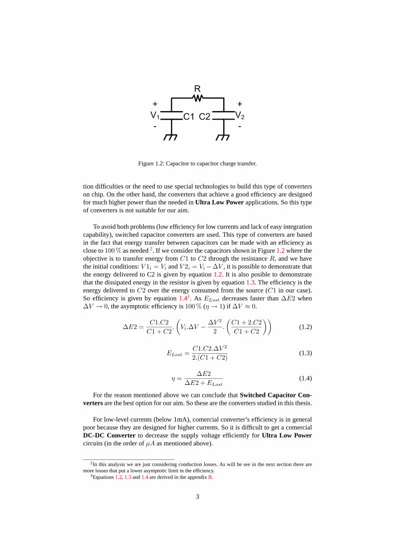
Figure 1.2: Capacitor to capacitor charge transfer.
tion difficulties or the need to use special technologies to build this type of converterson chip. On the other hand, the converters that achieve a good efficiency are designedfor much higher power than the needed inUltra Low Power applications. So this typeof converters is not suitable for our aim.
To avoid both problems (low efficiency for low currents and lack of easy integrationcapability), switched capacitor converters are used. This type of converters are basedin the fact that energy transfer between capacitors can be made with an efficiency asclose to100 % as needed2. If we consider the capacitors shown in Figure1.2where theobjective is to transfer energy fromC1 to C2 through the resistanceR, and we havethe initial conditions:V 1i = Vi andV 2i = Vi−∆V , it is possible to demonstrate thatthe energy delivered to C2 is given by equation1.2. It is also posible to demonstratethat the dissipated energy in the resistor is given by equation1.3. The efficiency is theenergy delivered toC2 over the energy consumed from the source (C1 in our case).So efficiency is given by equation1.43. As ELost decreases faster than∆E2 when∆V → 0, the asymptotic efficiency is100 % (η → 1) if ∆V ≈ 0.
∆E2 =C1.C2
C1 + C2.
(Vi.∆V − ∆V 2
2.
(C1 + 2.C2C1 + C2
))(1.2)
ELost =C1.C2.∆V 2
2.(C1 + C2)(1.3)
η =∆E2
∆E2 + ELost(1.4)
For the reason mentioned above we can conclude thatSwitched Capacitor Con-verters are the best option for our aim. So these are the converters studied in this thesis.
For low-level currents (below 1mA), comercial converter’s efficiency is in generalpoor because they are designed for higher currents. So it is difficult to get a comercialDC-DC Converter to decrease the supply voltage efficiently forUltra Low Powercircuits (in the order ofµA as mentioned above).
2In this analysis we are just considering conduction losses. As will be see in the next section there aremore losses that put a lower asymptotic limit in the efficiency.
3Equations1.2, 1.3and1.4are derived in the appendixB.
3

However, academic research has been developing the area for some years. [7] is avery important work that achieves very good efficiency levels forUltra Low Power ap-plications. [8] is the most recent work that achieves similar results in terms of efficiencyusing different architecture and control logic. [9] has a good efficiency in relation withthe conversion ratio (62 % of efficiency with a 1/5 conversion ratio) but has just oneconversion ratio. [10] has the peak of efficiency of66,7 % when the conversion ratio isapproximately0,6, but the controller consumes147,5µW 4 despite using subthresholdlogic. The specifications said that the minimum power to the load is400µW that istwo or three orders higher than the consumption of a micro-controller in sleep mode.Then, [11] has an single output voltage (444mV ) and a peak efficiency of56 % with aload current of285nA. Furthermore, if we supply a digital circuit with444mV we areworking in the subthreshold region for the technology used. [12] achieves an efficiencyfrom 37 % to 56 % but for currents from1µA to 4µA and has just one output voltagelevel.
All these works use particular architectures that are hardly able to include anotherconversion ratio. This work presents a novel architecture forSwitched Capacitor Con-verters that has the advantage of being modular and able to include more conversionratios if necessary. This feature makes the architecture very appropriate forDynamicVoltage Scaling. This is achieved presenting similar features in terms of efficiency incomparison with previous works. A novel technique to reduce dominant losses (para-sitic capacitances losses) is presented, that has the particularity of reducing such lossesas the number of conversion ratios is increased.
Summarizing the target application characteristics, the list of requirements for thiswork is:
Input voltage2,8V
Current load1µA - 100µA
Multiple conversion ratios with the same architecture
High efficiency (> 60 %)
1.2. General Considerations for Switched Capacitor Con-verters
In aSwitched Capacitor Converterthere are several capacitor configurations andthe times of duration of each configuration are called phases. An example of a basicSwitched Capacitor Converter is shown in Figure1.3. In Sub-Figure1.3(a)the con-verter is shown with all the switches opened, then in Sub-Figure1.3(b)the converter isshown in the configuration of phase one, and last in Sub-Figure1.3(c)in the phase two.
During phase one the two capacitors of the converter are connected in series to thevoltage source and each one is charged atVDD
2 . The output voltage is kept by the ca-pacitorCL. Then in the second phase the two capacitors are connected in parallel to
4Remember that the power consumption of the micro-controllers previously mentioned is approximatelythis value.
4

(a) Divider-by-two converter
(b) Divider-by-two converter during the firstphase configuration
(c) Divider-by-two converter during the se-cond phase configuration
Figure 1.3: Two phases divider-by-twoSwitched Capacitor Converterbasic example
5

capacitorCL and deliver to it the energy lost in the first phase and the needed by theload.
This cycle is repeated at a frequencyfsw. If the frequency and capacitors are suchthat the voltage in capacitors are essentially constant, the lost energy is negligible andthe efficiency of the converter is close to100 %.
This and other configurations can be seen in [7].
1.2.1. Losses In Switched Capacitor Converters
In the previous analysis a100 % asymptotic efficiency was mentioned. This waswithout considering some effects that cause an energy loss and a lower limit in theefficiency. This section analyzes the main types of losses.
Conduction Losses
As stated above, transfering charge from one capacitor to another (or from the sup-ply voltage to a capacitor) with a lower voltage has a loss in the resistance of the switchinvolved in the process. As can be seen in equations (1.2), (1.3) and (1.4) the smaller isthe voltage difference (∆V ) the more negligible are these losses. This type of energyloss is namedEcond.
Gate-drive Losses
To drive the gate of the switches that implement the different phases of the converterthere is a cost of energy. So to minimize this losses it is necessary to implement theswitches as small as possible. This type of energy loss is namedEgates.
Parasitic Capacitance Losses
When a floating capacitor is implemented in anIntegrated Circuit some parasiticcapacitances between the plates of the capacitor and the substrate appear. When the ca-pacitor changes the voltage of the plates with respect to the substrate, energy is wastedto charge and discharge these parasitic capacitances, because this energy is not delive-red to the load.
An example of floating capacitor implementation is with a poly1-poly2 capacitor.Figure1.4shows the capacitor and the parasitic capacitances involved.
Another way to implement a floating capacitor is using a PMOS capacitor (in aN-Well technology)5. This implementation has the advantage that the capacity per unitarea is higher than the first option (POLY1-POLY2), but has the disadvantage that ithas a non-linear behavior. The implementation is shown in Figure1.5where it can beseen that Drain, Source, and Bulk are one plate of the capacitor and the Gate is theother. The NWell-Substrate diode parasitic capacitance appears in this case.
5If we are using a N-Well technology it is necessary to use a PMOS transistor because the capacitor mustbe floating. As the NWell can float with respect to ground we must use a PMOS capacitor.
6

Figure 1.4: Bottom and top parasitic capacitances in a poly-poly capacitor.
Figure 1.5: PMOS capacitor implementation and parasitic capacitances.
The energy lost due to the charging and discharging of these parasitic capacitancesis namedEpar.
Logic Losses
To manage the switches of the converter a sequential logic is needed. The energysupplied to the logic circuits is not delivered to the load so it is important to minimizethese losses to have a good efficiency mainly when the power delivered to the load islow. This type of energy lost is namedElogic. We will include in this term also theenergy consumed by the analog circuits of the control block.
1.2.2. Efficiency
As the objective of aSwitched Capacitor Converter is to deliver energy to adevice using a different voltage than the input one, the efficiency is defined in terms ofenergy. So the efficiency is the ratio between energy delivered by the converter to theload and the energy taken by the converter from the supply voltage:
η =Eout
Ein=
Eload
Eload + Eloss(1.5)
7

where
Eloss = Econd + Egates + Epar + Elogic (1.6)
andEload is the energy delivered to the load.
1.2.3. Output Resistance
Figure1.6shows an equivalent circuit for a generalSwitched Capacitor Conver-ter . It is not possible to have a general theory to derive the output resistanceROUT .However it is posible to develop a general theory to calculate this resistance in the twolimit modes that aSwitched Capacitor Converter can work. These modes are theSlow Switching Limit (SSL from now on) and Fast Switching Limit (FSL from nowon) that are discussed in the Chapter 2 of [13].
It is considered that a givenSwitched Capacitor Converter is working in SSLwhen the switching frequency is slow enough to consider that currents are impulsive, orequivalently each phase of the converter has a time duration much bigger than the timeconstants (τ ) of the different topologies of the circuits. In this limit an equivalent outputresistance (RSSL) can be calculated, this calculation can be made with a general theorythat can be applied in allSwitched Capacitor Converters. This equivalent resistancehas the particularity of being inversely proportional to the switching frequency as canbe seen in equation (1.7). The constantKSSL is a function of the capacitor values,number of phases of the converter and the topology. In particular it is important tohighlight thatKSSL is a sum where each term is inversely proportional to a capacitorof the converter.
RSSL =KSSL
fSw(1.7)
On the other hand, it is considered that a givenSwitched Capacitor Converter isworking in FSL when the switching frequency is fast enough to consider that currentsare constant, or equivalently each phase of the converter has a time duration much lowerthan the time constants (τ ) of the different topologies of the circuits. Again in this limitan equivalent output resistance (RFSL) can be calculated with a general theory that canbe applied in allSwitched Capacitor Converters. This equivalent resistance has theparticularity of being independent of the switching frequency. The value of this resis-tance depends of the switches resistance, the number of phases of the converter and thetopology.
As mentioned above it is not possible to develop a general theory to calculate theoutput resistance in the range of frequencies where none of the two modes are valid.However an accepted approximation can be used as shows the equation (1.8).
ROUT '√
R2SSL + R2
FSL (1.8)
A deeper analysis of the output resistance calculations can be seen in the chaptertwo of [13].
8

Figure 1.6:Switched Capacitor Converterequivalent circuit.
9

10

CHAPTER 2
Proposed Architecture
The general idea of the architecture proposed in this thesis is to haven equal ca-pacitors connected in series and another capacitor connected in parallel with the load(CL from now on). One end of the series is always connected to ground. The otherend is connected to the source during one phase. The load andCL are connected to analternative node during the other phase. Therefore, the converter has two phases andn− 1 conversion ratios (as many as intermediate nodes in the series). Figure2.1showsa particular case withn = 5 and a conversion ratio of35 .
In the first phase (T1 from now on) shown in the Sub-Figure2.1(b) the source(VDD) is connected to the capacitor series, so the converter takes energy from the sour-ce and all the capacitors in the series have a voltageVDD
n . In this phaseCL gives chargeto the load and keeps the output voltageVOUT .
In the second phase (T2 from now on) shown in Sub-Figure2.1(c)one of the inter-mediate nodes of the series is connected to the load and the source is disconnected. Sothe converter gives charge to the load and returns toCL the charge taken by the loadduringT1 1. The conversion ratio is defined by the node where the load is connectedduring this phase.
Sub-Figure2.1(a)shows the series of capacitorsC1..C5, the capacitor connectedto the loadCL, the load represented by a current source, and the switchesSwT1 andSwT2 used in phasesT1 andT2 respectively. Then in Sub-Figures2.1(b)and2.1(c)are shown respectively the configuration in the two phases. If for example we want tohave a conversion ratio of45 we must connect the output to the node betweenC4 andC5.
The problem here is that duringT2 the capacitor composed by the seriesC1..C3is discharged (gives charge to the load andCL) while the capacitor composed by theseries ofC4 andC5 keeps the same charge. This difference of charge remains unchan-
1ExpressionsT1 andT2 are used to represent both the phase and the duration of each.
11

(a) Basic Converter
(b) Configuration during T1 (c) Configuration during T2
Figure 2.1: Example of converter with n = 5 and conversion ratio of 3/5
12

ged when in the next phaseT1, the total series is connected to the supply voltage andthe sum of voltages in the five capacitor isVDD. Therefore the voltage in the seriesC1..C3 will decrease every cycle and the output voltage too. The voltage in the seriesof capacitorsC4 andC5 has the opposite effect and will increase every cycle . So it isnecessary a way to replace this charge in the node where the load is connected.
To solve this problem, capacitors are rotated of position in the ring. So instead ofthinking about a series of capacitors it is better to imagine a ring which can be openedin every node. All the capacitors of the ring are associated to a switches configurationthat implement aBasic Capacitor Cell. Figure2.2shows that cell.
It can be seen that the top plate of the capacitor can be connected to the input andto the output through the switchesSwT1 andSwT2. It also shows that the ring can beopened with the switchSwInter and can be connected to ground through the switchSwGnd.
Figure2.3shows an example withn = 5 where the ring is composed by fiveBasicCapacitor Cells , Figure2.3(a)shows the ring with all the switches opened. Then in2.3(b)and2.3(c)the configuration of the ring before and after a rotation are shown. Inthe first one the ring is opened in theBasic Capacitor Cell of capacitorC5 and theoutput is connected through theBasic Capacitor Cellof capacitorC3. After the rota-tion the ring is opened in theBasic Capacitor Cellof capacitorC4 and the output isconnected through theBasic Capacitor Cellof capacitorC2. In this way all capacitorswill be connected to the supply voltage in a moment and will recover the charge.
The rotation of the ring causes a significant loss in parasitic capacitances, so thereis a trade-off between avoiding the rotation of the ring to minimize the mentioned los-ses, and the need to rotate the ring to replace the charge to the nodes where the loadis connected. This effect is illustrated in Sub-Figure2.11(a)showing the output vol-tage (VOUT ). In the first phaseT1 (bounded with two dotted lines) the ring is beingrotated and the load is taking charge fromCL, so the output voltage is decreasing. Inthe next phaseT2 (bounded with two dotted lines too) the output voltage is increasedby the charge given by converter toCL and the load. This process is repeated eighttimes before the next rotation. As can be seen in the first three periodsT1 + T2 theoutput voltage is increased, but because the discharging process above mentioned inthe next five periods the same will decrease. In this example the conversion ratio is 4
5and the supply voltage (VDD) is 2.8V. The rest of the waveforms will be explained next.
A discussion on which is the best way to implement the rotation will be introducedin Section2.3after the parasitic capacitances losses are analyzed.
2.1. Capacitors Implementation
Since the capacitors of the ring have essentially the same bias voltage it is posibleto use non-linear capacitors and keep the ratio between them (all equal in our case).So it is possible to use in parallel with the POLY1-POLY2 capacitors a PMOS ca-pacitor. This increases the capacitance per unit area because it is posible to build aPOLY1-POLY2 capacitor above a PMOS capacitor. The load capacitor (CL) needs nomatching so it is possible to use a combined device too.
13

Figure 2.2:Basic Capacitor Cell
This has an advantage because the bottom parasitic capacitance (POLY1-NWell)can be connected in parallel with the main capacitor and the top parasitic capacitan-ce (POLY2-NWell) is short-circuited (see Figure1.4). As a disadvantage the NWell-Substrate parasitic capacitance appears. Figure2.4shows the composed capacitor andthe parasitic capacitance.
2.2. Charge Transfer Analysis
Figure2.5 shows a general series ofn equal capacitors of valueC and the loadcapacitorCL. If we have a conversion ratio ofmn the equivalent circuit is a series oftwo capacitors:C1eq = C
m andC2eq = Cn−m . They can be seen in Figure2.5(b).
To understand the energy transmission in a cycle we will consider three phases:T1that gives us the initial conditions,T2 that transfers charge to the load andCL, andT1again because it is the phase when the supply voltage replaces the energy delivered bythe converter to the load.
After the first phaseT1, when the sourceVDD is connected,C1eq andC2eq havea chargeQ1i andQ2i respectively. To make a general analysisQ1i andQ2i are notnecessarily equal. So we have the equation:
VDD =Q1i
C1eq+
Q2i
C2eq(2.1)
During the phaseT2 the load andCL take a charge∆Q from C1eq. 2. Thus, thedifference between the charge ofC2eq andC1eq is ∆Q more than at the beginning. Sowe have the equation:
2The charge∆Q is the demanded by the load duringT2 and the necessary to replace the charge takenby the load fromCL during oneT1. So it is the total charge taken by the load in a cycleT1 + T2.
14

(a) Ring with fiveBasic Ca-pacitor Cells
(b) Before rotation (c) After rotation
Figure 2.3: Example of rotation in a fiveBasic Capacitor Cellsring
15

Figure 2.4: POLY1-POLY2 - PMOS composed capacitor.
(a) General converter (b) General converter equivalent
Figure 2.5: Power Transmission
16

Q2f −Q1f = Q2i −Q1i + ∆Q (2.2)
As Q1f andQ2f are the charge inC1eq andC2eq respectively in the second con-sidered phaseT1 they meet the following equation:
VDD =Q1f
C1eq+
Q2f
C2eq(2.3)
Now from (2.2) and (2.3)
VDD =Q2f −Q2i + Q1i −∆Q
C1eq+
Q2f
C2eq(2.4)
Thus
VDD −Q1i
C1eq= Q2f .
(1
C1eq+
1C2eq
)− Q2i
C1eq− ∆Q
C1eq(2.5)
And from (2.1) we have that
Q2i
C2eq= Q2f .
(1
C1eq+
1C2eq
)− Q2i
C1eq− ∆Q
C1eq(2.6)
Then
Q2i.
(1
C1eq+
1C2eq
)= Q2f .
(1
C1eq+
1C2eq
)− ∆Q
C1eq(2.7)
Or
Q2f = Q2i + ∆Q.
(C2eq
C1eq + C2eq
)(2.8)
Since the variation in the charge ofC2eq is given by the source, the charge takenfrom the source during the second considered phaseT1 to replace the charge taken bythe load andCL during phaseT2 is:
∆QVDD= ∆Q.
(C2eq
C1eq + C2eq
)(2.9)
For all devices we have that:
∆E =∫
V.I.dt (2.10)
In the case of the source the voltage is constant so the delivered energy is:
∆EVDD=∫
VDD.I.dt = VDD.
∫I.dt = VDD.∆QVDD
(2.11)
From (2.9) and (2.11)
∆EVDD= VDD.∆Q.
(C2eq
C1eq + C2eq
)(2.12)
17
To calculate the energy taken by the load in the cycle we do not have a constantvoltage, but if we think in capacitors as big as necessary to have essentially a constantvoltage in all of them we can say that the equation (2.10) in the case of the load is
∆ELoad = VOUT .∆Q (2.13)
As can be seen from figure2.5the no load output voltage isV NLOUT = VDD.
(C2eq
C1eq+C2eq
).
As capacitors are considerer as big as necessary we have thatVOUT = V NLOUT . So using
equation2.13:
∆ELoad = VDD.
(C2eq
C1eq + C2eq
).∆Q (2.14)
And the efficiency is:
η =∆ELoad
∆EVDD
= 1 (2.15)
As we have considered a general case it is possible to conclude that the architectureproposed has an asymptotic ideal efficiency of100 % for all the conversion ratios.
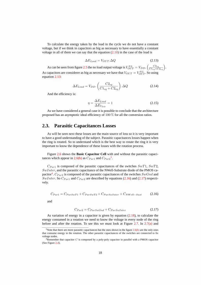
2.3. Parasitic Capacitances Losses
As will be seen next these losses are the main source of loss so it is very importantto have a good understanding of the subject. Parasitic capacitances losses happen whenthe ring is rotated. So to understand which is the best way to rotate the ring it is veryimportant to know the dependence of these losses with the rotation process.
Figure2.6 shows theBasic Capacitor Cellwith and without the parasitic capaci-tances which appear in2.6(b)asCPar1 andCPar2
3.
CPar1 is composed of the parasitic capacitances of the switchesSwT1, SwT2,SwInter, and the parasitic capacitance of the NWell-Substrate diode of the PMOS ca-pacitor4. CPar2 is composed of the parasitic capacitances of the switchesSwGnd andSwInter. SoCPar1 andCPar2 are described by equations (2.16) and (2.17) respecti-vely.
CPar1 = CParSwT1 + CParSwT2 + CParSwInter + CNWell−Sust (2.16)
and
CPar2 = CParSwGnd + CParSwInter (2.17)
As variation of energy in a capacitor is given by equation (2.18), to calculate theenergy consumed in a rotation we need to know the voltage in every node of the ringbefore and after the rotation. To see this we must look at Figure2.7. In 2.7(a)and
3Note that there are more parasitic capacitances but the ones shown in the figure2.6(b)are the only onesthat consume energy in the rotation. The other parasitic capacitances of the switches are connected to fixvoltage nodes.
4Remember that capacitorC is composed by a poly-poly capacitor in parallel with a PMOS capacitor(See Figure2.4).
18

(a) Basic capacitor cell without parasitic ca-pacitances
(b) Basic capacitor cell with parasitic capa-citances
Figure 2.6: Parasitic capacitance of aBasic Capacitor Cell
2.7(b) we can see the ring configuration before and after a rotation respectively. Wewill analyze the general case when the ring is open in theBasic Capacitor Cellof thecapacitorCn and after the rotation we open the ring in theBasic Capacitor Cellof agenericCp capacitor of the ring.
∆EC =C
2.(V 2
f − V 2i
)(2.18)
In Figure2.7(a)we can see that the bottom plate of capacitorC1 is connected toground through the switchSwGnd of the capacitorCn. The input (VDD) is connectedduring T1 through the switchSwT1 of the capacitorCn. So it is simple to see thatthe voltage in the top plate of the capacitorC1 is VDD. 1
n , in C2 is VDD. 2n , etc. So for
CPar1 we have that:
VCP ar1i(k) = VDD.
(k
n
); ∀k = 1 : n (2.19)
In the case ofCPar2 it is the same with the exception ofCn because this node isconnected to ground. So forCPar2 we have that:
VCP ar2i(k) =
VDD.(
kn
)∀k = 1 : n− 1
0 k = n(2.20)
In Sub-Figure2.7(b) we can see that the bottom plate ofCp+1 is connected toground through the switchSwGnd of the capacitorCp. The input (VDD) is connectedduringT1 through the switchSwT1 of the capacitorCp. We can see that the voltagein the top plate ofCp+1 is VDD. 1
n and so on toCn that has a voltage in the top plateof VDD.n−p
n . Equally we can see that top plate ofCp is VDD and so on toC1 whohas a voltage in the top plate ofVDD.n−p+1
n . Summarizing the final voltage of everyparasitic capacitorCPar1 is:
VCP ar1f (k) =
VDD.(
k+n−pn
)∀k = 1 : p
VDD.(
k−pn
)∀k = p + 1 : n
0 < p < n (2.21)
19

(a) Ring before rotation (b) Ring after rotation
Figure 2.7: Ring configuration changes in a rotation
20

In the case ofCPar2 it is the same with the exception ofCp because this node isconnected to ground. So forCPar2 we have that:
VCP ar2f (k) =
VDD.(
k+n−pn
)∀k = 1 : p− 1
VDD.(
k−pn
)∀k = p : n
0 < p < n (2.22)
Thus from equations (2.18), (2.19) and (2.21) we have that:
∆ECP ar1(k) =CPar1
2.V 2
DD.
[(
k+n−pn
)2
−(
kn
)2] ∀k = 1 : p[(k−p
n
)2
−(
kn
)2] ∀k = p + 1 : n
0 < p < n
(2.23)From equation (2.23) we can see that the energy variation in parasitic capacitors
from C1 to Cp is positive and negative in the rest. This is because in the first caseparasitic capacitors are receiving energy form the source and in the second one they arethrowing the energy to ground. So to calculate the energy consumed from the sourcewe have:
∆ECP ar1Total =p∑
k=1
∆ECP ar1(k) =CPar1
2.V 2
DD.
p∑k=1
[(k + n− p
n
)2
−(
k
n
)2]
(2.24)And from equations (2.18), (2.20) and (2.22) we have that:
∆ECP ar2(k) =CPar2
2.V 2
DD.
[(k+n−p
n
)2
−(
kn
)2] ∀k = 1 : p− 1[(k−p
n
)2
−(
kn
)2] ∀k = p : n− 1[(k−p
n
)2
− 0]
k = n
0 < m < n
(2.25)From equation (2.25) we can see that the energy variation in parasitic capacitors
from Cp to Cn−1 is negative and positive in the rest. This is because in the first caseparasitic capacitors are throwing to ground the energy and in the second one they arereceiving energy form the source. In steady-state the energy received form the sourceis equal to the one thrown to ground. So to calculate the energy consumed from thesource we can do it using the negative terms of equation (2.25) and multiplying themby -1. So we have that:
∆ECP ar2Total =n−1∑k=p
∆ECP ar2(k) =CPar2
2.V 2
DD.n−1∑k=p
[(k
n
)2
−(
k − p
n
)2]
(2.26)From equations (2.24) and (2.26) we can see that the consumption of a rotation of
the ring has a dependency withp. This is equivalent to say that it has a dependency withthe number of places that the capacitors are shifted in each rotation. To know which is
21

the best way to rotate the ring it is enough to know the dependence withp of the sumsthat appear in both equations. These sums will be calledsumCPar1 andsumCPar2respectively. Figure2.8shows the value of the sums as function ofp for converters offive, six, and sevenBasic Capacitor Cells, where is clear that the best choice is toshift one place each capacitor in each rotation so the election isp = n− 15.So for the choice taken equations (2.24) and (2.26) become:
∆ECP ar1Total =CPar1
2.V 2
DD.n−1∑k=1
[(k + 1
n
)2
−(
k
n
)2]
or
∆ECP ar1Total =CPar1
2.V 2
DD.
(1− 1
n2
)(2.27)
and
∆ECP ar2Total =CPar2
2.V 2
DD.
n−1∑k=n−1
[(k
n
)2
−(
k − (n− 1)n
)2]
or
∆ECP ar2Total =CPar2
2.V 2
DD.
(n− 1
n
)2
(2.28)
Thus
∆ECP arTotal =CPar1
2.V 2
DD.
(1− 1
n2
)+
CPar2
2.V 2
DD.
(n− 1
n
)2
(2.29)
2.4. Rotation Technique to Reduce Parasitic Capacitan-ces Losses
Since parasitic capacitances losses are the main reason for losses in the converterand therefore the fall in efficiency, a detailed analysis of this issue for the chosen caseof rotation (p = n − 1) is made in this section. Then the implemented technique todecrease these losses is presented.
Figure2.9 shows the state of the parasitic capacitances before and after the rota-tion. In Sub-Figure2.9(a)the state of all the parasitic capacitances before the rotationis shown.CPar1 n voltage isVDD andCPar2 n voltage is zero6. Parasitic capacitances
5From Figure2.8 it is clear that it is exactly the same to choosep = 1 or p = n − 1 so the electionp = n − 1 is arbitrary. Furthermore this choice has no impact on other aspects as logic or switchingconsumption, etc.
6Remember that parasitic capacitancesCPar1 andCPar2 of aBasic Capacitor Cellare short-circuitedif the interconnection switch is closed. See Figure2.6.
22

(a) SumCPar1 and SumCPar2 for a fiveBasic Capacitor Cellsconverter as function of p.
(b) SumCPar1 and SumCPar2 for a sixBasic Capacitor Cellscon-verter as function of p.
(c) SumCPar1 and SumCPar2 for a sevenBasic Capacitor Cellsconverter as function of p.
Figure 2.8: SumCPar1 and SumCPar2 for different number ofBasic Capacitor Cellsconverter.
23

CPar1 n−1 andCPar2 n−1 are short-circuited and have a voltage ofn−1n .VDD. The
rest of parasitic capacitances are in a similar situation but with the other fractions ofthe supply voltage (n−2
n .VDD , n−3n .VDD, etc).
In Sub-Figure2.9(b)the state of all the parasitic capacitances after the rotation pro-cess is shown. It can be seen that capacitorsCPar1 n andCPar2 n−1 have lost energywhile the rest of the parasitic capacitances have gained energy. In steady state the men-tioned energy lost byCPar1 n andCPar2 n−1 is equal to the energy gained by the restof the parasitic capacitances7.
Equations (2.27) and (2.28) where derived assuming that the parasitic capacitancesthat lose energy during the rotation throw that energy to ground. Instead it is possibleto make a redistribution of that charge to the parasitic capacitances that need to gainenergy. Or, what is the same, the parasitic capacitances that need to lose energy cando it delivering energy to the parasitic capacitances that need to gain energy. For thisthe order in which the rotation sequence is performed is critical. Figure2.10shows theprocess.
Preparation For the Rotation Process
As capacitors of the ring (C1, C2,....Cn) are much larger than parasitic capaci-tances they can be considered as constant voltage source. Before the first step of therotation it is needed that all the capacitors of the ring be floating and separate from thering the capacitor whose parasitic capacitances will lose energy (Cn in Figure2.10).So all switchesSWGnd must be kept opened during the rotation process and bothSwInter that connectCn to the ring must be kept opened. This situation is shown inSub-Figure2.10(a).
First Step in the Rotation Process
As energy lost in the energy transfer between two capacitors is proportional to thesquare of the difference in the initial voltage (Equation1.3) the less is the differen-ce the less is the energy lost. So the first step is to connect the parasitic capacitanceCPar1 n to the parasitic capacitanceCPar1 n−1 that have less difference of voltage.That difference isVDD
n . The mentioned situation is shown in Sub-Figure2.10(b). Asmentioned the capacitors of the ring can be considered as constant voltage sources, soif we consider only the variations in the parasitic capacitances the equivalent circuit isequal to the one shown in Figure1.2, whereC1 (the capacitor that delivers energy) isthe parallel ofCPar1 n andCPar2 n−1 andC2 (the capacitor that takes energy) is theparallel of the rest of the parasitic capacitances.
If we defineCPar = CPar1 + CPar2 then we have that:C1 = CPar andC2 =(n− 1).CPar. The energy lost in the first step is (using equation1.3):
ELost1 =C1.C2.∆V 2
2.(C1 + C2)=
CPar.(n− 1).CPar.∆V 2
2.(CPar + (n− 1).CPar)=
CPar.(n− 1).V 2DD
2.n3
(2.30)7This is because in steady-state the converter as a whole can’t win energy.
24

(a) State before the rotation. (b) Stare after the rotation.
Figure 2.9: State of the parasitic capacitances before and after the rotation.
25

(a) Cn capacitor separation. (b) First step. (c) Second step.
Figure 2.10: Rotation process.
26

Rest of Steps in the Rotation Process
The second step is to connect parasitic capacitanceCPar1 n to the parasitic capa-citanceCPar1 n−2 (see Sub-Figure2.10(c)). The difference of voltage is againVDD
nand the equivalent circuit is the same as the first step. So the loss of energy is again theshown in equation (2.30).
This process is repeated untilCPar1 n is connected to the bottom plate of the ca-pacitorC1 so the number of steps isn. Then the energy lost in the whole process isn.ELost1:
ELostRotation =CPar
2.V 2
DD.(n− 1)
n2
or
∆E∗CP arTotal =
CPar1
2.V 2
DD.(n− 1)
n2+
CPar2
2.V 2
DD.(n− 1)
n2(2.31)
with
∆E∗CP ar1Total =
CPar1
2.V 2
DD.(n− 1)
n2(2.32)
and
∆E∗CP ar2Total =
CPar2
2..V 2
DD.(n− 1)
n2(2.33)
Figure2.11shows an example of 5Basic Capacitor Cellsring rotation. In Sub-Figure2.11(a)the output voltage waveform and the top plate of the five capacitors ofthe ring are shown. Then in Sub-Figure2.11(b)a zoom of the process of rotation (seethe time axis) shows how the voltage of the capacitorC5 go down pulling up the restof the capacitors.
2.5. Energy Saved with Improved Rotation Technique
The energy saved with the technique can be computed comparing equations (2.29)and (2.31).In particular we can compare the contributions ofCPar1 andCPar2 separa-tely for each way of rotation. So we will see the expressions :
∆E∗CP ar1Total
∆ECP ar1Total=
n− 1n2
.n2
n2 − 1=
1n + 1
(2.34)
and
∆E∗CP ar2Total
∆ECP ar2Total=
n− 1n2
.
(n
n− 1
)2
=1
n− 1(2.35)
The comparison is made in the table2.1as function of the number of capacitors ofthe ring (n). If we want to analyze the case of a fiveBasic Capacitor Cellsconverter,
27

(a) Output voltage and top plate voltages of the ring capacitors.
(b) Zoom of the top plate voltages in the rotation process.
Figure 2.11: Output and top plate voltages.
28
we must see the second row and it can be seen that the contribution ofCPar1 decreaseto 16,7 % in comparison with the original mechanism of rotation. In the case of theCPar2 the contribution decrease to25 %. AsCPar1 (having the NWell-Substrate diodeparasitic capacitance) is much bigger thanCPar2 the main contribution to the parasi-tic capacitances losses comes fromCPar1. Thus the total power consumption in theparasitic capacitances will be reduced to close to17 %.
n 1n+1
1n−1
4 0.200 0.3335 0.167 0.2506 0.143 0.2007 0.125 0.167
Table 2.1: Comparison of the two implementations of the rotation
2.6. The Control Logic
Figure2.12 shows an schematic diagram of the logic used in the particular caseof the designed converter. There is a “One Hot”8 block that works as a pointer to theBasic Capacitor Cell in which the ring must be opened.
The block “Non Overlapping Clock Generator” generates from the main clock sig-nal two non overlapped signals (T1 andT2) used to drive the gates of the switchesSwT1 andSwT2.
The block “SwT1 Block” uses the signalT1 and the outputs of the different FlipFlops (Q0...Q4) to generate the five signals to drive the the gates of the switchesSwT1.Basically it passes the signalT1 only to theBasic Capacitor Cell that is pointed bythe “One Hot”.
The block “SwT2 Block” uses the signalT2, the outputs of the different Flip Flops(Q0...Q4), and the signalsSel0 andSel1 to generate the five signals to drive the gatesof the switchesSwT2. It works similar to the block “SwT1 Block” but passes the sig-nalT2 only to theBasic Capacitor Cellthat connects the ring to the output node. ThesignalsSel0 andSel1 are used to select the conversion ratio as is shown in the table2.2.
At last, the block “Rotation Block” implements the rotation of the ring. This hap-pen when the block “Frequency Divider by Eight” enables the rotation. The signalsSwParBCC0...SwParBCC0 are used to drive the switches that implement the para-sitic capacitances losses reduction technique. These switches are connected as a “star”to the top plates of the different capacitors of the ring. The block uses a secondarysignal clock with a fourteen times faster frequency than the main clock one. The blockimplements the rotation as described in the section2.4 in the following order:
1. Open the switchSwGnd that was closed and the switchSwInter that will re-main open after end of the rotation.
8A “One Hot block” is a ring of Flip Flops D that one of them has a one logic stored. Each clock edgethe one logic is stored in the next Flip Flop of the ring.
29

Sel1 Sel0 Conv.Ratio
0 0 1/50 1 2/51 0 3/51 1 4/5
Table 2.2: Conversion ratio selection.
2. Implement the technique of reduction of parasitic capacitances losses.
3. Close the switchSwInter that was opened before the start of the rotation pro-cess.
4. Close the switchSwGnd that will remain closed after the end of the rotation.
5. Generates a signal used to shift the “One Hot”
2.7. Chapter Summary
Basic ideas were first presented and then the first problem to solve, that is the ina-bility to return the charge to the point where the load is connected. This problem wassolved implementing a mechanism of rotation that basically consist in changing theposition of all the capacitors of the converter systematically.
For implementing the converter and the rotation a switches configuration was de-fined for each capacitor of the ring. The basic set “capacitor-switches configuration”was namedBasic Capacitor Cell.
Then the implementation of the capacitors was presented. After this a charge trans-fer analysis was made.
The calculation of the parasitic capacitances consumption was made and, as thisconsumption is the most significant power loss, a technique to reduce it was proposed.The consumption of the parasitic capacitances was calculated again for the case whenthis technique is applied. Both results were compared having as a result that the propo-sed technique has a significant decrease in the parasitic capacitances losses.
At last, a brief analysis of the logic implementation was presented.
30

Figure 2.12: Block diagram of control logic.
31

32
CHAPTER 3
Numerical Model
Electrical simulations of medium-complexity circuits have long simulation timesand are not suitable for design space exploration. In these cases it is helpful to have anumerical model that allows us to explore the design space automatically and at reaso-nable times. This chapter shows the numerical model developed for the converter withthe purpose of exploring the design space.
A very important feature of the developed model is that it allows the designer toperform a design space exploration of any technology with little work. All the designerneeds are some curves extracted from electrical simulation and some parameters of thetechnology.
First, the chapter shows the general considerations for the model, then the develop-ment of the model for the two phases. Finally, it shows how losses were modeled. Inthe appendixA the matlab files tree and the way to introduce the information requiredfor other technologies are presented.
3.1. General Considerations for the Model
Since voltage-oriented models in circuits with non-linear capacitances can have cu-mulative errors as is described in [14], it is better to have a charge-oriented model, sothis was the model used. Given that PMOS capacitors and switch resistances are non-linear the model developed is non-linear.
As mentioned, we used a charge-oriented model so the state variables are the char-ge of the capacitors. There aren + 1 capacitors of whichn make up the ring and theremaining one isCL.
Figure3.1 shows the converter for which the model was developed. Throughoutthis section am
n conversion ratio is considered with0 < m < n.
33

Equations used in the Matlab code are highlighted with double box.
3.1.1. Non-linear Capacitors
The non-linearity of the model comes from the fact that every capacitor is compo-sed by a linear capacitor (poly1-poly2) in parallel with a non-linear capacitor (PMOS).So the equation that describes this combined device is:
Q = QLinear + QPMOS = Cpoly.V + QPMOS(V ) (3.1)
WhereQPMOS(V ) is described with a curve extracted from electrical simulations,so equation (3.1) must be solved numerically.
3.1.2. Switches Resistances
Resistance of CMOS switches are calculated from two curves(one for PMOS andone for NMOS transistors) extracted from electrical simulations. These curves have theresistance per width unit (inΩ.µm)1 as function of the source (drain) voltage. The gatevoltage is supposed constant, equal to the supply voltage (2,8V ) of the converter.
The curves were introduced in a matrix into a user defined function. This function,that uses linear interpolation needs the width of the transistor, the type of transistor (“n”or “p”), and source (drain) voltage. The function returns the resistance of the transistor.
To calculate the resistance of a complementary switch (one “n” transistor in parallelwith a “p” transistor) it is necessary to calculate the two resistances separately and thencalculate the parallel equivalent.
3.1.3. Representation in the State Space
If−→Q is the state vector composed by the charge of then +1 capacitors,VDD is the
source voltage andIL the load current, equation3.2 shows the general model for theconverter. Functionf is different for each phase (T1 andT2) so we will develop twodifferent functions which we will call
−→f T1 and
−→f T2.
−→Q =
Q1
...Qm−1
Qm
Qm+1
...Qn
QL
=
f1(−→Q,−→u )...
fm−1(−→Q,−→u )
fm(−→Q,−→u )
fm+1(−→Q,−→u )...
fn(−→Q,−→u )
fL(−→Q,−→u )
=−→f (−→Q,−→u ) (3.2)
With:−→u = (VDD, IL)
1As all switches were designed with minimum length the only geometrical parameter considered is thewidth.
34

Figure 3.1: NBasic Capacitor CellsConverter
35

To develop a numerical model we must make the following approximation:
−→Q ' ∆
−→Q
∆t(3.3)
Where∆t is a differential time. So if we want to solve the differential equation ineach phase inNumSteps steps we have the following equations∆t = T1
NumSteps or
∆t = T2NumSteps that are equal in our case becauseT1 = T2 = TSW
2 .
∆−→Q =
−→Q(t + ∆t)−
−→Q(t) (3.4)
So from equations (3.2), (3.3) and (3.4) we have that:
−→Q(t + ∆t) '
−→Q(t) +
−→f (−→Q,−→u ).∆t
Or for numerical models:
−→Q(k + 1) =
−→Q(k) +
−→f (−→V (−→Q(k)), u).∆t
With:
−→V (−→Q) =
Vn(Q1)...
Vm+1(Qm−1)Vm(Qm)
Vm−1(Qm+1)...
V1(Qn)VCL
(QCL)
WhereVk(Qk) ∀k = 1 : n andVCL
(QCL) means the dependence of the voltage
of the capacitor with its own charge. The dependence off with Q was written in thisway because it is more convenient for the equations developed in next sections.
So
Q1(k + 1)...
Qm−1(k + 1)Qm(k + 1)
Qm+1(k + 1)...
Qn(k + 1)QCL
(k + 1)
=
Q1(k)...
Qm−1(k)Qm(k)
Qm+1(k)...
Qn(k)QCL
(k)
+
f1(−→V (−→Q(k)),−→u )
...
fm−1(−→V (−→Q(k)),−→u )
fm(−→V (−→Q(k)),−→u )
fm+1(−→V (−→Q(k)),−→u )...
fn(−→V (−→Q(k)),−→u )
fCL(−→V (−→Q(k)),−→u )
∆t (3.5)
The output for the two phases is given by:
VOUT = VCL(QCL
) (3.6)
36

Here it is important to notice that despite in all the equations the supply voltageis considered as a parameter that can be changed, this change must take into accountthe data extracted from electrical simulations. In particular the switches resistancesand the buffers consumption are extracted from electrical simulations for a particularsupply voltage, so it is needed to make a different extraction for each supply voltagevalue. Look appendixA for more details.
3.2. Phase T1
The equivalent circuit for the phaseT1 is shown in figure3.2(a)so we have thenext equations:
ICn = . . . = ICm+1 = ICm = ICm−1 = . . . = IC1 = Qk; ∀k = 1 : n (3.7)
˙QCL = ICL = −IL (3.8)
VDD =n∑
r=1
VCr (Qr) +n−1∑z=1
VRz + VRSwGnd+ VRSwT1 (3.9)
If we make the following definition:
RT1 =n−1∑z=1
Rz + RSwGnd + RSwT1 (3.10)
From equations (3.7), (3.9), (3.10) and the Ohm law we have that:
VDD =n∑
r=1
VCr(Qr) + RT1.Qk; ∀k = 1 : n (3.11)
So
Qk =
[VDD −
n∑r=1
VCr(Qr)
].
1RT1
; ∀k = 1 : n (3.12)
Using equations (3.8) and (3.12) we have the function−→f (−→Q,−→u ) in the phaseT1:
−→f T1(
−→Q,−→u ) =
[VDD −∑n
r=1 VCr (Qr)] . 1RT1
...[VDD −
∑nr=1 VCr
(Qr)] . 1RT1
[VDD −∑n
r=1 VCr (Qr)] . 1RT1
[VDD −∑n
r=1 VCr (Qr)] . 1RT1
...[VDD −
∑nr=1 VCr
(Qr)] . 1RT1
−IL
(3.13)
Therefore the equation to use in the numerical model during the phaseT1 is:
37

QT11 (k + 1)
...QT1
m−1(k + 1)QT1
m (k + 1)QT1
m+1(k + 1)...
QT1n (k + 1)
QT1CL
(k + 1)
=
QT11 (k)
...QT1
m−1(k)QT1
m (k)QT1
m+1(k)...
QT1n (k)
QT1CL
(k)
+
[VDD −
∑nr=1 VCr (Q
T1r (k))
]. 1RT1
...[VDD −
∑nr=1 VCr
(QT1r (k))
]. 1RT1[
VDD −∑n
r=1 VCr (QT1r (k))
]. 1RT1[
VDD −∑n
r=1 VCr(QT1
r (k))]. 1RT1
...[VDD −
∑nr=1 VCr
(QT1r (k))
]. 1RT1
−IL
.∆t
(3.14)
3.3. Phase T2
The equivalent circuit for the phaseT2 is shown in Figure3.2(b)so we have thenext equations:
ICm = ICm−1 = . . . = IC1 = Qk; ∀k = 1 : m
0 = ICn = . . . = ICm+1 = Qk; ∀k = m + 1 : n(3.15)
QCL = ICL = −(IL + Qk); ∀k = 1 : m (3.16)
VOUT =m∑
r=1
VCr(Qr) +
m−1∑z=1
VRz+ VRSwGnd
+ VRSwT2 (3.17)
If now the make the following definition:
RT2 =m−1∑z=1
Rz + RSwGnd + RSwT2 (3.18)
From equations (3.6), (3.15), (3.17), (3.18) and the Ohm law we have that:
VCL(QCL
) =m∑
r=1
VCr(Qr) + RT2.Qk; ∀k = 1 : m (3.19)
and
Qk =
[VCL
(QCL)−
m∑r=1
VCr(Qr)
].
1RT2
∀k = 1 : m (3.20)
So from equations (3.15) and (3.20) we have that
Qk =
[VCL(QCL
)−∑m
r=1 VCr (Qr)] . 1RT2
∀k = 1 : m
0 ∀k = m + 1 : n(3.21)
Then form equations (3.16) and (3.20):
38

(a) T1 phase equivalent circuit. (b) T2 phase equivalent circuit.
Figure 3.2: NBasic Capacitor Cellsring circuits for numerical model
39

QCL =
[m∑
r=1
VCr (Qr)− VCL(QCL
)
].
1RT2
− IL (3.22)
Using equations (3.21) and (3.22) we have the function−→f (−→Q,−→u ) in the phaseT2:
−→f T2(
−→Q,−→u ) =
[VCL(QCL
)−∑m
r=1 VCr (Qr)] . 1RT2
...[VCL
(QCL)−
∑mr=1 VCr
(Qr)] . 1RT2
[VCL(QCL
)−∑m
r=1 VCr (Qr)] . 1RT2
0...0
[∑m
r=1 VCr(Qr)− VCL
(QCL)] . 1
RT2− IL
(3.23)
Then
QT21 (k + 1)
...QT2
m−1(k + 1)QT2
m (k + 1)QT2
m+1(k + 1)...
QT2n (k + 1)
QT2CL
(k + 1)
=
QT21 (k)
...QT2
m−1(k)QT2
m (k)QT2
m+1(k)...
QT2n (k)
QT2CL
(k)
+
[VCL(QCL
)−∑m
r=1 VCr(Qr)] . 1
RT2...
[VCL(QCL
)−∑m
r=1 VCr(Qr)] . 1
RT2
[VCL(QCL
)−∑m
r=1 VCr(Qr)] . 1
RT2
0...0
[∑m
r=1 VCr(Qr)− VCL
(QCL)] . 1
RT2− IL
.∆t
(3.24)
3.4. Energy Losses
There are essentially four types of energy losses that were presented in section1.2.This section describes them and shows how they were estimated.
3.4.1. Parasitic Capacitances Losses
As derived in section2.4, the equation (2.31) describes the losses in charging anddischarging the parasitic capacitances. So this one is the equation used.
3.4.2. Gate-drive Losses
To calculate Gate-drive losses two curves extracted from electrical simulations we-re used, one for “n” transistors and the second one for “p” transistors. These curveshave the switching losses per width unit (inJouls/µm)2 as function of the source
2As all switches were designed with minimum length the only geometrical parameter considered is thewidth.
40

(drain) voltage.
The curves were introduced in a matrix into a user defined function. This functionneeds the width of the transistors of the switch (the “n” and the “p”) and source (drain)voltage. It returns the energy consumed in a on-off cycle of the switch.
3.4.3. Conduction Losses
There are two equivalent resistors (see equations (3.10) and (3.18)) that dissipateenergy, each one associated with one phase of the converter. As the equations (3.14)and (3.24) were solved step by step, the resistance was calculated in every step to takeinto account its dependence on system state. So to calculate the dissipated energy wemust use for each step the equation:
∆ERT i(k) = RTi(k).i2RT i
(k).∆t i = 1 : 2 (3.25)
Then, the energy dissipated in one period of switching (T1 + T2) is:
ET1+T2ResLoss =
NumSteps∑k=i
(RT1(k).i2RT1
(k).∆t)
+NumSteps∑
k=i
(RT2(k).i2RT2
(k).∆t)
(3.26)
3.4.4. Digital and Analog Control Circuits Losses
The Digital Circuits losses are considered in two different ways. The first one is thelogic consumption that is needed to implemente the two phases of the converter. Thesecond one is the logic consumption to implement the rotation process. It is needed tohave these two values to calculate the performance of the circuit.
After each execution of the phasesT1 andT2 the logic consumption used to im-plement these phases is added in a variable that accumulate the total logic losses. Thesame happens when a rotation is performed with the logic consumption used to imple-ment the rotation.
As mentioned in the introduction, analog circuit losses are considered into the logiclosses. The bias current considered is100nA so the energy si calculated as:
EAnalog = VDD.IBIAS .(tf − ti) (3.27)
WhereIBIAS is the total bias current of the analog circuits, andti andtf are theinitial and final time where the power was integrated.
3.5. How the Model Works
For the model we have two kind of magnitudes: those associated to the dynamicof charging and discharging capacitors that have variation with continuous time, andthose associated to events such as closing and opening switches that are associated todiscrete times. This section describe all the considered magnitudes and shows how the
41

model integrates them to calculate the performance of the circuit. It exists in the modelthe possibility to calculate the performance in steady state or including the transient.
3.5.1. Magnitudes That Change With Each Time Step
Charge
Q is the vector that contains the charge of then + 1 capacitors of the converter(see equation (3.2)). From this magnitude are obtained voltage and current. Voltage iscalculated from equation (3.1) and current deriving in time.
Energy Taken from Supply Voltage
As the energy taken from the supply voltage is given by equation (2.11), it is neededto calculate duringT1 the charge taken from the source. DuringT2 no current is takenby the core of the converter from the supply voltage (the analog circuits, gate driveand the logic take energy from the supply voltage but these losses are considered in adifferent way). AfterT1 the energy calculated is added to the cumulative energy valuetaken from the source.
Resistances
To have an accurate transient and dissipated energy in resistors it is necessary tocalculate the resistancesRT1 andRT2 dynamically so are calculated every∆t timesduringT1 andT2 respectively.
Energy Dissipated in Resistances
The energy dissipated inRT1 andRT2 is calculated integrating numerically duringT1 andT2 respectively using equation3.26. After each phase the energy calculated isadded to the cumulative energy value dissipated in the resistances.
3.5.2. Magnitudes That Change With Events
Energy Dissipated in SwitchesSWT1 and SWT2
After the execution ofT1 the energy consumed in the cycle of opening and closingthis switch is calculated. Then this value is added to a variable that stores the accumu-lated wasted energy.Exactly the same happens withSWT2.
Energy Dissipated in Switches Associated to Rotation (SWInt y SWGnd)
After a rotation the energy consumed in the cycle of opening and closing the swit-chesSWInter andSWGnd is calculated. Then this value is added to a variable thatstores the accumulated wasted energy.
Energy Dissipated Charging Parasitic Capacitances in the Rotation
After a rotation the energy consumed in charging and discharging parasitic capaci-tances is calculated. Then, this value is added to a variable that stores the accumulatedwasted energy.
42

Figure 3.3: Model Pseudo Code
Energy Dissipated In Control Circuits
After the execution ofT1 andT2 the energy consumed by the logic in this cycle isadded to a variable that stores the accumulated wasted energy. After the execution of arotation the energy consumed by the logic in this process is added to the same variable.
The energy needed to supply the analog circuits is calculated at the end of thesimulation and added to the accumulated value too.
3.5.3. Model Pseudo Code
Figure3.3 shows the pseudo code used, where it can be seen that there is awhilestatement that eliminates the transient in an iterating process. Inside thewhile state-ment there is afor instruction that runsNumRotations times, that is the number ofrotations of the ring that wants to be included in the simulation. Then, there is aforstatement that runsNumPeriods which is the number of periods (T1 + T2) that thesimulator runs before making the rotation of the ring. At last there are twofor state-ments that runNumSteps times, which implementT1 andT2.
43

In the last rotation the state is saved in order to be used to start the next simulation,if necessary. At the end of thewhile (simulation has been completed) the temporalmean of the charge in capacitorCL is compared with the same value of the previoussimulation. If there is a significant difference it is because the transient has not been re-moved so the simulation starts again but in the state saved in the last rotation. Thus, thesimulator simulates the converter as many times as necessary to remove the transientand calculate the performance in steady-state. When the comparison of the temporalmean of the charge ofCL of two consecutive simulations is negligible, the transienthas been removed so it is no longer necessary to continue iterating.
Inside thefor statements that implements step by step the phasesT1 andT2 theassociated resistance is calculated and then the charge variations using equations (3.14)and (3.24).
3.6. Comparison with Electrical Simulations
In order to know how accurate the model is, a comparison between electrical andnumerical simulations is made in this section. These simulations were made for theconverter designed with a conversion ratio of4
5 , a current load of50µA, a switchingfrequency of500kHz andN = 8. The energy was computed integrating the power ina period of80µs in steady-state. The comparison between both simulations is shownin the Table3.1where the following parameters are shown :
VRipple(mV ) - Ripple voltage.
EL(J) - Energy delivered to the load.
ECparCond(J) - Energy lost in conduction and parasitic capacitances losses.
ELog(J) - Energy lost in the logic.
ESw(J) - Energy lost in gate driving
eff (%) - Efficiency ( EL
EL+ECparCond+ELog(J)+ESw).
Here it is important to highlight that the parasitic capacitances and conduction los-ses are presented in a single variable. This is because although both losses have verydifferent origins, the two are evidenced in the same way, namely power dissipation inthe switches, so they are difficult to separate in electrical simulations.
In the table it can be seen that the differences between both simulations are small.In particular the efficiency has a difference of1 %.
On the other hand, while the numerical model has a low accuracy when the effi-ciency is low (less than20 %) the accuracy is very good for all the efficiency levels ofinterest for the designer. So the model is very good for making a first order analysisand taking decisions shown in the next section.
Figures3.4shows the output voltage waveforms for two rotations of the ring. Whilethe simulation is made in a time window of80µA what is equivalent to eight rotationsof the ring, in the Figure just two rotations are shown.
44

Parameter VRipple(mV ) EL(J) ECparCond(J) ELog(J) ESw(J) eff ( %)Electrical Sim. 21 8.13e-9 1.71e-9 5.33e-10 4.12e-10 77.85Numerical Sim. 17 7.85e-9 1.51e-9 5.28e-10 3.00e-10 77.00
Table 3.1: Comparison between electrical and numerical simulations
Figure 3.4:VOUT waveforms for numerical and electrical simulations.
3.7. Design Space Exploration for OptimumN Selec-tion
The number of periods between consecutive rotations of the ring (N ) impactsmainly in two of the energy losses of the converter The larger the value ofN is theless the output average voltage for a given conversion ratio and a given load currentis. As the conduction loss depends on the difference between the real output voltageand the ideal output voltage, the bigger is the value ofN the bigger are the conductionlosses. So to minimize conduction losses we must minimize the value ofN . On theother hand, the larger the value ofN is the less the parasitic capacitances losses are,so there is a trade-off between conduction and parasitic capacitances losses that can bemanaged with the value ofN .
To know which is the best value ofN for the converter designed, a design spaceexploration was made with variations in the load current, conversion ratio, switchingfrequency andN . To decide the best value ofN , the analysis is made for a load current
45

Figure 3.5: Efficiency as a function ofN@IL=100µA.
of 100µA because it is the largest current for which the converter was designed. In thechapter where the feedback loop is analyzed it will be seen that for minor currents theefficiency will keep essentially constant.
Figure3.53 shows the efficiency for this current load for the cases of conversionratio of4/5 and1/5 (the largest and the smallest conversion ratios). In the case of con-version ratio of4/5 it can be seen that the peak of efficiency is achieved for a value ofN higher than the one shown in the figure. On the other hand, for the case of conver-sion ratio of1/5 the peak of efficiency is achieved in the caseN = 9. In digital circuitshaving frequencies derived from the main clock is much easier when this derivation ismade by powers of two. SoN = 8 is the best choice for the designed converter becauseit has an efficiency that is near the peak in the case of conversion ratio of1/5 and it hasa very good efficiency in the caso of4/5. So the caseN = 8 is the one chosen.
As this space design exploration was made before the implementation of the techni-que to decrease the parasitic capacitances losses, the efficiency values are significantlylower than in the final design.
3Although in the graphs a continuous line can be seen the only purpose that it has is to shows the trend.The only points that have a real sense are those for whichN ∈ N.
46

CHAPTER 4
Proposed Control Scheme
In this chapter a feedback loop is proposed. This control mechanism will allow usto achieve the two main aims of aDC-DC Converter . The most basic aim of aDC-DC Converter is to supply a constant voltage to the load. Another important aim is tohave a constant efficiency independent of the current load.
If we are looking for applications such as supply of micro-controllers and use thetechniqueDynamic Voltage Scalingto minimize the power consumption without ha-ving a negative impact in the performance of the circuit, a constant efficiency is needed.If for example the converter has a good efficiency for high currents (ηActive) but a badefficiency for low currents (ηSleep), the real average efficiency of the converter in theapplication will be good or bad depending of the relationship of the duration betweensleep and active modes (TSleep andTActive) and the power consumption in both modes(PSleep andPActive). Equation (4.1) shows the expression of the combined efficiency.So having an efficiency independent of the load power (or equivalently independent ofthe load current) is necessary to avoid having an efficiency that depends on the appli-cation.
ηComb =PActive.TActive + PSleep.TSleep
PActive.TActive
ηActive+ PSleep.TSleep
ηSleep
(4.1)
Thinking in the more basic aim that is having a constant output voltage, Figure1.6shows an equivalent circuit for aSwitched Capacitor Converter . To have a constantoutput voltage it is necessary to have a constant voltage drop in the output resistan-ce ROUT for all load currents. As stated in section1.2.3 the output resistance has acomponent independent of the switching frequency (RFSL) and another that varies in-versely proportional to it (RSSL). To know which one is the best mode for working(fast or slow switching limit) we must analyze the implications of each one.
Fast Switching Limit (FSL) mode implies that each phase has a very short duration(much less than the different time constants (τ ) of the different topologies) and this
47

will have a negative impact in the efficiency because the logic, parasitic capacitancesand gate-drive losses will be very high. Furthermore, in this mode the output resistanceis independent of any parameter that can be controlled in real time1 so regulation ofthe output voltage is very difficult because the drop voltage in the output resistance isdependent of the current load. So working in this mode must be avoided.
On the other side, Slow Switching Limit (SSL) implies that each phase has a verylong time duration (much longer than the different time constants (τ ) of the differenttopologies), enough to consider that the voltage waveforms are square. In this case thetime to transfer energy between capacitors or between the supply voltage and the capa-citors is enough to consider that capacitors achieve the steady-state. So it is clear thatthis mode is more appropriate because it allows to transfer energy with a minimum ofenergy losses in logic, gate drive and parasitic capacitances. Furthermore, in this modethe output resistance has an inversely proportional dependence with the switching fre-quency that is a parameter that can be changed in real time.
However, it is important to note that the energy transferred to a capacitor is in-dependent of the transient and only depends of the initial and final conditions. So ifwe have phase durations for example of ten time constants (τ = T1/10) the voltageachieved by the capacitors will be in the99,995 % of the asymptotic final value. But ifwe decrease the switches width to half of the original case, the new time constants aremultiplied by two(τ∗ = T1/5), so the phases have a time duration of approximately5.τ∗ and the final voltage will be in the99,326 % of the asymptotic final value whatis essentially the same. But if we consider the gate drive losses the second case hasjust the50 % of consumption than in the first case. So the optimum point to design aSwitched Capacitor Convertermust be in the transition where none of the two modesare valid.
As stated at the beginning of this chapter, a feedback loop will be proposed. Theproposed one consists in changing the switching frequency as a function of the loadcurrent. So to achieve the maximum target current delivered to the load (100µA) thedesign is made in the “optimum” point for this case. When the current load decreasesthe frequency will decrease and the operation mode will be going into the SSL. Wewill demonstrate that this feedback loop will allow us to achieve a constant efficiency.However it can be improved if we make smaller the switches when the frequency be-comes lower, or equivalently if we use switches with a width proportional to the loadcurrent. This improvement was not implemented but this optimization will be analyzedin section6.1.
4.1. Feedback Loop Analysis
As mentioned in the previos paragraph, the converter will work in the SSL and inthe limit where no one of the two asymptotic limits are valid, the SSL resistance isdominant. So for us the output resistance in the Figure1.6will be inversely proportio-nal to the switching frequency. If this is the case the drop voltage in the resistance isVDrop = ROUT .IL or VDrop = KSSL
fSw.IL. So it is clear that to have an output voltage
1This resistance just depends on switch resistances and the topologies of the converter.
48

independent of the current load it is necessary to have a switching frequency proportio-nal to the current load. Thus iffSw = KIL
.IL the voltage drop in the output resistancebecomes constant with the valueVDrop = KSSL
KIL. It is clear that when the load current
(and as consequencefSw) is increasing andR(fSSL) becomes negligible in compari-son withRFSL the output voltage will start to decrease independent of the switchingfrequency because the drop voltage in the resistance would beVDrop = RFSL.IL. Orequivalently, the converter is working in FSL.
To analyze the effect in the efficiency of having a switching frequency that has alinear dependence with the current load, the efficiency of a general converter can bewritten from equations (1.5) and (1.6) as:
η =Eout
Ein=
Eload
Eload + Econd + Egates + Epar + Elogic(4.2)
Here we have that all the losses have a linear dependence with the switching fre-quency with the exception of the logic losses that can have both a frequency de-pendence factor and a constant factor due to the bias current of analog circuits su-ch as amplifiers or comparators. In the case of the energy delivered to the load ifwe consider that the output voltage is approximately constant, it can be written asELoad = VOUT .IL.∆t or Eload = KLoad.fSw where∆t is the period of time wherethe power was integrated andKLoad = VOUT .∆t
KIL. And the equation (4.2) can be written
as:
η =KLoad.fSw
KLoad.fSw + Kcond.fSw + Kgates.fSw + Kpar.fSw + K1Logic.fSw + K2Logic
or
η(fSw) =KLoad
KLoad + Kcond + Kgates + Kpar + K1Logic + K2Logic
fSw
(4.3)
From equation (4.3) it is clear that if the termK2Logic
fSwis negligible in comparison
with the other terms of the denominator the efficiency is independent of the switchingfrequency. This assumption is valid for a wide range of the switching frequency. Whenthe switching frequency is such that the previous assumption is not valid and the swit-ching frequency continues decreasing the efficiency will start to degrade. On the otherhand, if the switching frequency becomes high and the converter goes into the FSLmode, the output voltage will decrease when the load current becomes higher. Thus,the efficiency starts to decrease and will collapse.
Because of the above, the proposed feedback loop is the one shown in Figure4.1.The difference voltage (Vd) between the output voltage (VOUT ) and a voltage reference(VREF ) is amplified with an operational amplifier. The output voltage of the amplifieris connected to the input of a Voltage Controlled Oscillator (VCO from now on). Theoutput of the VCO is connected to the main clock of the converter. Thus, if the loadcurrent starts to increase, the output voltage will decrease. As a consequenceVd andthe output of the amplifier will increase. Then the output frequency of the VCO willincrease and the output voltage will increase, returning to the original value.
49

Figure 4.1: Proposed feedback loop.
4.2. VREF Optimum Value
The efficiency of the converter has a strong dependence with the reference outputvoltage. For a given converter, load current,N andVREF the switching frequency isgiven. If we increaseVREF the feedback loop is going to increase the frequency to de-crease the difference voltage. So the conduction losses will decrease (less voltage dropin the output resistance) but the other losses will increase (larger switching frequency).On the other hand, if we decreaseVREF the feedback loop will decrease the switchingfrequency and effect in losses will be the opposite. So there is an optimumVREF .
To calculate the optimum value ofVREF we must open the loop and make varia-tions in the switching frequency. These variations will make variations in the outputresistance and as consequence in the average output voltage. In a switching frequencyfOPT
Sw the output average voltage will beV OPTOUT and the efficiency will be maximum.
If when we close the loop we use as a voltage reference the optimum output averagevoltage (VREF = V OPT
OUT ) the feedback loop will adjust the switching frequency tofOPT
Sw and the efficiency will be optimum. Figure4.2 shows this analysis made withMatlab for the designed converter, a conversion ratio of4
5 , N = 8 andIL = 50µA. Inthe upper graphic it can be seen that the optimum value ofVREF in this case is' 2V .In the bottom graphic the losses are shown as percentage of the total losses. This grap-hic shows how for the highest output voltages the frequency is too high and the logic,parasitic capacitances and gate drive losses are dominant. On the other hand, for thelowest output voltages the voltage drop in the output resistance is high and conductionlosses are dominant.
4.3. About the Feedback Loop
Here it is important to highlight that the feedback loop as such can oscillate, havehigh overshoot or very long settling times. So to design the amplifier and the VCO asmall signal model of the converter must be developed. The union amplifier-VCO doesimplement the controller, so the small signal model of the converter must be with the
50

Figure 4.2: OptimumVREF selection.
51

form:
VOUT = H(s).fSw (4.4)
Such a model is out of the scope of this thesis but should be obtained either byanalysis or simulations in order to design the loop gain.
52

CHAPTER 5
Results and Comparison with Other Works
In this chapter the designed converter is presented. First, the dimensions of all themain components are shown. Then, a detailed analysis of the performance of the con-verter for the four conversion ratios is performed. At last, the global performance ofthe converter is presented and a comparison with existing works is made, in particularan analysis of the main differences.
5.1. Results
The presented converter was designed and simulated with the technologyOn −Semi 0,5µm. Table5.1 shows the data converter designed with exception of buffersdimensions and logic. Then, Figure5.1shows the efficiency of the converter as a func-tion of the load delivered power for the conversion ratios2/5 and4/5.
Figure5.2shows the performance of the converter for the conversion ratio4/5. Acomparison between the performance with and without the parasitic losses reductiontechnique is performed. In the upper graphic the efficiency is shown and it can be seenthat the value is significantly lower when the reduction technique is not applied. Theexplanation of this difference can be seen in the graphics where the losses are shownas percentage of total losses. In the case where the losses reduction technique is notapplied the dominant losses are the parasitic capacitances losses. When the techniqueis applied the parasitic capacitances losses significantly decrease, and the dominantlosses are the conduction losses. Gate driving losses are the less significant in all thecurrent load range for both cases.
If we look at the efficiency in the case when the losses reduction technique is ap-plied it is clear that it is approximately constant in the current load range10− 100µA.This is a consequence of the switching frequency variaton proportionally to the currentload (This dependence between current load and switching frequency was emulatedbecause the feedback loop was not implemented).When the current load is in the range
53

Parameter Unit Value Comment
wCL µm 2000 Width of the load capacitorCL.lCL µm 2000 Length of the load capacitorCL.CL nF 13 Load capacitor.wCRing µm 1000 Width of the ring capacitorsCRing.lCRing µm 1000 Length of the ring capacitorsCRing.CRing nF 3.25 Ring Capacitors (there are five of this one.)wnSWInter µm 247 Width of the n transistor of the switchSWInter.wpSWInter µm 619 Width of the p transistor of the switchSWInter.wnSWT2 µm 22.6 Width of the n transistor of the switchSWT2.wpSWT2 µm 56.4 Width of the p transistor of the switchSWT2.wpSWT1 µm 56.4 Width of the p transistor of the switchSWT1.wnSWGnd µm 247 Width of the n transistor of the switchSWGnd.fSw@100µA MHz 1 Switching frequency.IBIAS nA 100 Current that foresees the implementation of analog circuits.n Unit 5 Number of capacitors that implement the ring.VDD V 2.8 Supply Voltage
Table 5.1: Designed converter parameters. Technology usedOn− Semi 0,5µm
Figure 5.1: Efficiency vs load power.
54

0,1− 10µA the efficiency decreases because the constant term (K2Logic) in the equa-tion (4.3) becomes more significant1. This can be seen in the graphic where the lossesare shown, where the logic losses come to be dominant in this range of currents. Onthe other hand, if we look at the efficiency for the highest current values (60, 80 and100µA) it is clear that it has a gentle downward trend. This is because the resistanceof FSL mode (RFSL) starts to be more significant and the mechanism described in theChapter4 to keep the drop voltage constant in the output resistance starts to be noteffective.
Then, if we look the case ofIL = 200µA it is clear that the output voltage andthe efficiency have an abrupt reduction. This is because the operation mode of the con-verter is much near the FSL than for the caseIL = 100µA. Another interpretationthat can be made for this behavior is in terms of voltage waveforms. While in the caseof IL = 100µA the phases duration is enough to consider that the different capacitorvoltages achieve the steady state (T1 ' 3.τ ), in the caseIL = 200µA the frequencybecomes twice with respect to the other case and the phases duration is not enough toachieve steady-state in capacitor voltages (T1 ' 1,5.τ ). As a consequence the outputvoltage decreases and the conduction losses too.
On the other hand, there is a similar situation in the case of the application of theparasitic capacitances losses reduction technique. Phases duration are too short andthere is no time to redistribute the charge between the parasitic capacitances that needsto lose energy and the ones that need to gain it. So the parasitic capacitances losses in-crease too. In the graphic where the losses are shown these effects can be seen, whereboth type of losses have increased abruptly for this value of load current.
In the graphic where the average output voltage is shown it is clear that the me-chanism to keep the output voltage constant works very well in the current range400nA − 10µA so we can conclude that the output resistance is inversely propor-tional to the switching frequency and the converter is working in SSL mode. However,in the range10−100µA the output voltage starts to decrease. As stated in the previousparagraph the resistanceRFSL starts to be more significant and the transition betweenSSL and FSL modes starts. Unlike the graph showing the efficiency which containstwo curves, here only one curve is presented because applying the reduction losses te-chnique has no effect on the output voltage.
Figures5.3, 5.4and5.5shows the performance of the converter for the conversionratios of 3/5, 2/5 and 1/5 respectively. The situation is practically the same for all thecases with the exception of the fact that the lesser the conversion ratio is the lesser theefficiency for a given load current is. This is because for a lower conversion ratio thepower delivered to the load is lower while the logic, parasitic capacitances and gatedrive losses keeps equal.
5.2. Comparison with Other Works
Although some works about this topic in the literature exist, just [7] and [8] havevery similar specifications with this work, so the comparison is made with these two.
1This term comes from the integration of the power of analog circuits such as amplifiers of comparators(100nA in this case).
55

Figure 5.2: 4/5 conversion ratio performance.
56

Figure 5.3: 3/5 conversion ratio performance.
57

Figure 5.4: 2/5 conversion ratio performance.
58

Figure 5.5: 1/5 conversion ratio performance.
59
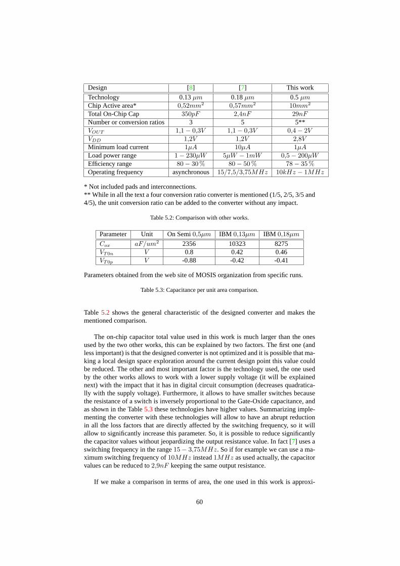
Design [8] [7] This work
Technology 0.13µm 0.18µm 0.5µmChip Active area* 0,52mm2 0,57mm2 10mm2
Total On-Chip Cap 350pF 2,4nF 29nFNumber or conversion ratios 3 5 5**VOUT 1,1− 0,3V 1,1− 0,3V 0,4− 2VVDD 1,2V 1,2V 2,8VMinimum load current 1µA 10µA 1µALoad power range 1− 230µW 5µW − 1mW 0,5− 200µWEfficiency range 80− 30 % 80− 50 % 78− 35 %Operating frequency asynchronous 15/7,5/3,75MHz 10kHz − 1MHz
* Not included pads and interconnections.** While in all the text a four conversion ratio converter is mentioned (1/5, 2/5, 3/5 and4/5), the unit conversion ratio can be added to the converter without any impact.
Table 5.2: Comparison with other works.
Parameter Unit On Semi0,5µm IBM 0,13µm IBM 0,18µm
Cox aF/um2 2356 10323 8275VT0n V 0.8 0.42 0.46VT0p V -0.88 -0.42 -0.41
Parameters obtained from the web site of MOSIS organization from specific runs.
Table 5.3: Capacitance per unit area comparison.
Table 5.2 shows the general characteristic of the designed converter and makes thementioned comparison.
The on-chip capacitor total value used in this work is much larger than the onesused by the two other works, this can be explained by two factors. The first one (andless important) is that the designed converter is not optimized and it is possible that ma-king a local design space exploration around the current design point this value couldbe reduced. The other and most important factor is the technology used, the one usedby the other works allows to work with a lower supply voltage (it will be explainednext) with the impact that it has in digital circuit consumption (decreases quadratica-lly with the supply voltage). Furthermore, it allows to have smaller switches becausethe resistance of a switch is inversely proportional to the Gate-Oxide capacitance, andas shown in the Table5.3 these technologies have higher values. Summarizing imple-menting the converter with these technologies will allow to have an abrupt reductionin all the loss factors that are directly affected by the switching frequency, so it willallow to significantly increase this parameter. So, it is possible to reduce significantlythe capacitor values without jeopardizing the output resistance value. In fact [7] uses aswitching frequency in the range15− 3,75MHz. So if for example we can use a ma-ximum switching frequency of10MHz instead1MHz as used actually, the capacitorvalues can be reduced to2,9nF keeping the same output resistance.
If we make a comparison in terms of area, the one used in this work is approxi-
60

Parameter [7] This Work
Typeofdata Measured SimulationVOUT /VDD 0,667 0,714Load Power 100µW 100µWEfficiency 76,3 % 77,9 %Conduction Losses 12,45µW 11,1µWParasitic Losses 7,47µW 6µWGate drive Losses 6,38µW 5,15µWControl Losses 4,69µW 6,67µW
Table 5.4: Performance comparison in a particular situation.
mately twenty times larger than the one used by the other works. Taking into accountthat the area is in general dominated by capacitors in this type of circuits, this big dif-ference again can be explained in terms of technology differences. First of all, becausethe capacitors used in this work are based on PMOS capacitors and the Gate-Oxidecapacitance per unit area is approximately four times larger for the others technolo-gies, simply changing the technology will allow to reduce the area to one quarter. Thisreduction is made keeping the same total capacitor value. In addition, because what ismentioned in the previous paragraph this change of technology would allow to reducesignificatively the total capacitor value. If this reduction could be made in the order offive times smaller, the total area of capacitors will be reduced twenty times that is theabove mentioned difference.
The other parameters have similar values with exception of supply voltage andswitching frequency. The switching frequency was analyzed previously so we will dis-cuss the difference in supply voltage. The main reason of this difference is due to thedifferent threshold voltage (VT0) of the technologies. This parameter puts a low limit tothe supply voltage given by the equation (5.1) ( [15]) whereVT0n andVT0p are the th-reshold voltage for transistorsn andp respectively, andnn andnp are the subthresholdslope factor of the transistorn andp respectively. The objective of this minimum limitis to avoid the gap that can exist in the conduction of the switch if there is a strip wherenone of the two transistors are conducting. The values ofVT0 are shown in Table5.3where it can be seen that theOn− Semi0,5µm technology has a larger value in bothtypes of transistors. As mentioned, the supply voltage has a quadratic direct impact inthe logic consumption so the difference in this parameter of the technology (VT0) hasa very important impact.
V MinDD =
nn.VT0p + np.VT0n
nn + np − nn.np(5.1)
At last, in a particular situation a comparison with [7] is performed. Table5.4showsthis comparison, where it can be seen that for a very similar situation (almost equalconversion ratio and equal load power) not only the efficiency has a very similar value,but the four types of losses have very similar values.
61

62

CHAPTER 6
Conclusions and Future Work
A novel architecture for aUltra Low Power Switched Capacitor DC-DC Con-verter was proposed. This architecture is modular (each module was named asBasicCapacitor Cell ) and allows to add easily new conversion ratios if needed. An exampleof a Switched Capacitor Converterwith five Basic Capacitor Cellswas implemen-ted and electrically simulated. This simulation was made for the four conversion ratiosand for currents from400nA to 100µA. The efficiency achieved is above77 % forone order of magnitude of the current load for the conversion ratio4/5. The efficiencyachieved is comparable with the existing works in the literature mainly [7] and [8].
A feedback loop mechanism was proposed. It consist in changing the switching fre-quency proportionally to the current load. It allows to have just the needed switching(in logic and switches) having a constant efficiency in a wide range of load currents.The proposed control is built regulating the output voltage with an operational amplifierand a VCO (Voltage Controlled Oscillator). The frequency of the waveform providedby the VCO, which is proportional to the load current, is connected to the main clockof the converter. Because the feedback loop was not implemented it was emulated inthe electrical simulations. The result was a set of curves of efficiency that has a planarbehavior in a wide range of currents for all the conversion ratios.
As parasitic capacitances losses are dominant, a novel technique to reduce theselosses was implemented. This technique results in an improvement approximately of10 % in the efficiency from a80 % reduction in the mentioned losses.
A generical numerical model was developed that is useful to make design spaceexploration. As the architecture is modular and the model uses some electrical parame-ters extracted from electrical simulations and parameters of the technology, it is easyto adapt the model for other technologies.
Although the comparison with the existing works in the literature has as result thata similar performance is reached, a much larger total capacitor value and a larger area
63

were used. This difference is explained in terms of the used technology. A first orderanalysis was made, showing that both differences can be significantly reduced just im-plementing the converter in more modern technology.
6.1. Future Work
Although the general performance of the converter is very similar to the one ofexisting works, it was paying a significative price in area and total capacitance, makingit difficult to compare. To have a more realistic comparison, implementing a converterusing the proposed architecture in a more appropriate technology is central.
The logic was implemented but not optimized. As shown for example in Figure5.2for low currents the losses in the logic are dominant, so making an optimization in thispart of the circuit can achieve an increase in the general efficiency and a decrease inthe minimum load current.
The designed converter was achieved from electrical simulations, analyzing the dif-ferent losses and changing parameters to improve them. So it is not sure that the designpoint chosen is the better. A design space exploration must be made to analyze if abetter design exists.
As mentioned in Chapter4 a small signal-model must be developed for the conver-ter in order to make a design of the controller that ensures the stability of the feedbackloop.
If the feedback loop is implemented, when the load current decreases the switchingfrequency decreases too, but the different components of the converter (switches andcapacitors) remain the same, in particular the time constants (τ ) of the different pha-ses remain equal. But if the switching frequency is reducing the time constants canbe increased too without jeopardizing the average output voltage and the efficiency ofthe converter. The increase inτ can be implemented increasing the capacitors or theswitches resistances. As increasing capacitors affects the output resistance it is betterto make a reduction in the switches width. This allows to improve the efficiency due toa decrease in the gate drive losses. [8] uses a similar mechanism subtracting or addingswitches in parallel as needed.
At last, future work should also include fabricating and testing the converter.
64

Bibliography
[1] A. Sedra and K. Smith,Microelectronic Circuits, 4th ed. Oxford UniversityPress, 1999.
[2] L. Yuan and G. Qu, “Analysis of energy reduction on dynamic voltage scaling-enabled systems,”Computer-Aided Design of Integrated Circuits and Systems,IEEE Transactions on, vol. 24, no. 12, pp. 1827–1837, 2005.
[3] P. Artillan, M. Brunet, D. Bourrier, J.-P. Laur, N. Mauran, L. Bary, M. Dilhan,B. Estibals, C. Alonso, and J.-L. Sanchez, “Integrated lc filter on silicon for dc-dcconverter applications,”Power Electronics, IEEE Transactions on, vol. 26, no. 8,pp. 2319 –2325, aug. 2011.
[4] S. Musunuri, P. Chapman, J. Zou, and C. Liu, “Design issues for monolithic dc-dcconverters,”Power Electronics, IEEE Transactions on, vol. 20, no. 3, pp. 639 –649, may 2005.
[5] J. Wibben and R. Harjani, “A high efficiency dc-dc converter using 2nh on-chipinductors,” inVLSI Circuits, 2007 IEEE Symposium on, june 2007, pp. 22 –23.
[6] M. Wens and M. Steyaert, “An 800mw fully-integrated 130nm cmos dc-dc step-down multi-phase converter, with on-chip spiral inductors and capacitors,” inEnergy Conversion Congress and Exposition, 2009. ECCE 2009. IEEE, sept.2009, pp. 3706 –3709.
[7] Y. Ramadass and A. Chandrakasan, “Voltage scalable switched capacitor dc-dcconverter for ultra-low-power on-chip applications,” inPower Electronics Spe-cialists Conference, 2007. PESC 2007. IEEE. IEEE, 2007, pp. 2353–2359.
[8] O. A.-T. Hasib, M. Sawan, and Y. Savaria, “A low-power asynchronous step-down dc-dc converter for implantable devices,”IEEE Transactions on BiomedicalCircuits and Systems, vol. 5, no. 3, June 2011.
[9] A. Viraj and G. Amaratunga, “A monolithic cmos 5v/1v switched capacitor dc-dcstep-down converter,” inPower Electronics Specialists Conference, 2007. PESC2007. IEEE. IEEE, 2007, pp. 2510–2514.
65

[10] L. Su, D. Ma, and A. Brokaw, “Design and analysis of monolithic step-downsc power converter with subthreshold dpwm control for self-powered wirelesssensors,”IEEE Transactions on Circuits and Systems I: Regular Papers, vol. 57,no. 1, pp. 280–290, Dec. 2010.
[11] M. Wieckowski, G. Chen, M. Seok, D. Blaauw, and D. Sylvester, “A hybrid dc-dc converter for sub-microwatt sub-1v implantable applications,” in2009 Sympo-sium on VLSI Circuits. IEEE, 2009, pp. 166–167.
[12] S. Grubery, H. Reinisch, G. Hofer, A. Missoni, W. Pribyl, and G. Holweg, “Ahybrid dc/dc converter for ultra-low power wireless sensor nodes,” in2011 7thConference on Ph. D. Research in Microelectronics and Electronics (PRIME).IEEE, 2011, pp. 97–100.
[13] M. Seeman, “A design methodology for switched-capacitor dc-dc converters,”2009.
[14] D. Ward and R. Dutton, “A charge-oriented model for mos transistor capacitan-ces,”Solid-State Circuits, IEEE Journal of, vol. 13, no. 5, pp. 703–708, 1978.
[15] E.A.Vittoz, ”Micropower Techniques”in Design of VLSI Circuits for Telecommu-nications and Signal Processing. Prentice Hall, 1993.
66

APPENDIX A
Numerical Model Data Construction
This appendix describes the different user defined functions used in the numericalmodel in Matlab. FigureA.1 shows the files used tree.
A.1. File Tree
This section describes each defined function and the data that the user must intro-duce. The explanation of each input and output of the different functions is made ineach file.
A.1.1. FunctionPerformanceFinal.m
This is the main function that calculates the performance of the converter. It cal-culates the charge in all the capacitors as function of time and the different energiesinvolved as energy delivered to the load, parasitic capacitances lost energy, etc. Fromthis data it calculates the efficiency and output voltage waveform. How this functionworks it is described in Section3.5.
Technology Necessary Data
It is not necessary to introduce technology data in this file because all the dataneeded is taken by the file amis05um.m.
A.1.2. amis05um.m
This file have the objective of concentrate some technology data used by the model.
Technology Necessary Data
Wnmin [µm] - Minimum width of n transistor.
Wpmin [µm] - Minimum width of p transistor.
67

Figure A.1: Files Tree
68

DeltaEInverter [Jouls/µm] - Energy per width unit consumed in a On-Off cycleof an inverter. This data must be extracted from electrical simulation. It is veryimportant that it takes into account the fun-out used in the drivers of the switches.If for example all the inverters have as load another inverter four times widtherthis must be taken into account in the simulation used to extract the data.
DeltaELogicT1T2 [Jouls] - Energy consumed by the logic in each process ofon-off of the both switchesSWT1 y SWT1.
DeltaELogicRot [Jouls] - Energy consumed by the logic in each process of rota-tion of the ring.
CnArea [F/µm2] - Parasitic capacitance per area unit of the drain/source of ntransistors.
CnPer [F/µm] - Parasitic capacitance per length(perimeter) unit of the drain/sourceof n transistors.
CpArea [F/µm2] - Parasitic capacitance per area unit of the drain/source of ptransistors.
CpPer [F/µm] - Parasitic capacitance per length(perimeter) unit of the drain/sourceof p transistors.
LDSn [µm] - Length of the drain/source area of n transistors.
LDSp [µm] - Length of the drain/source area of p transistors.
CPolyArea [F/µm2] - Capacitance per area unit of ploy1-poly2 capacitors.
CPolyPer [F/µm] - Capacitance per length(perimeter) unit of ploy1-poly2 ca-pacitors.
CNWellSust [F/µm2] - Parasitic capacitance per area unit of the NWell-Substratediode.
A.1.3. QdeVs05um.m
This function calculates the charge of a PMOS capacitor as a function of the biasvoltage and his length and width.
Technology Necessary Data
This function uses a two rows matrix (“f” in the .m file), the data is extractedfrom electrical simulation. The electrical simulation must be made with large capacitors(1000 ∗ 1000µm2 for example). The numerical simulation do not take into account theeffective length or width so minimal transistors must be avoided.
Capacitor Voltage [V ] (First row) - Voltage between plates of the capacitor.
Charge [Coulomb/µm2] (Second row) - Charge per area unit.
A.1.4. VsdeQPMosPoly.m
This function returns the voltage of a capacitor composed by a poly1-poly2 and aPMOS capacitor.
69

Technology Necessary Data
CPolyArea [F/µm2] - Capacitance per area unit of ploy1-poly2 capacitors.
CPolyPer [F/µm] - Capacitance per length(perimeter) unit of ploy1-poly2 ca-pacitors.
A.1.5. VsdeQ05um.m
Implements the inverse function ofQdeVs05um.m.
Technology Necessary Data
The data needed is the same that the functionQdeVs05um.mneeds, but the rowsof the matrix must be interchanged.
A.1.6. CalcRT1.m
This function calculates the equivalent resistance for the phaseT1 described in theequation3.10
Technology Necessary Data
It is not necessary to introduce technology data in this file.
A.1.7. ResMos05um.m
This function calculates the resistance of a single switch (one transistor). To calcu-late the resistance of a composed switch it is necessary to call the function two timesand calculate the parallel equivalent.
Technology Necessary Data
The necessary data for this function is the resistance per width unit for n and for ptransistors. It uses a three rows matrix (named “f1” in the file), the data of the matrix isextracted from electrical simulations.
Source Voltage [V ] (First row) - Source bias voltage.
n resistance [Ω.µm](Second row) - n transistors resistance per unit width.
p resistance [Ω.µm](Third row) - p transistors resistance per unit width.
It is important to notice that these data is extracted for a given supply voltage(VDD). To makes a numerical simulation with other value ofVDD, an electrical si-mulation must be made and the data introduced in the matrix “f1” again.
A.1.8. fIteracionT1.m
This function implements the equation3.13
70

Technology Necessary Data
It is not necessary to introduce technology data in this file.
A.1.9. deltaESwitchesBuffers.m
This function calculates the switches consumption including the buffers consump-tion. Although no technology data is needed in this file, two design criteria must beincluded. The first one is the fun-out (“funout” in the .m file) of the inverters that mustbe equal for all them. The second one is the ratio between the width of the n and ptransistors (“wpsobrewn” in the .m file) in the different inverters. If for example theinverters where designed having the p transistor witdh two times larger than the one ofthe n transistor this parameter must be 2.
Technology Necessary Data
It is not necessary to introduce technology data in this file.
A.1.10. deltaESwitches.m
This function calculates the consumption of driving the gates of the switch transis-tors not including the buffers consumption.
Technology Necessary Data
It uses a three row matrix (named “f” in the .m file), the matrix data is extractedfrom electrical simulations.
Source Voltage [V ] (First row) - Source bias voltage.
n transistor gate drive consumption [Jouls/µm](Second row) - Consumptionper width unit of driving the n transistor gate.
p transistor gate drive consumption [Jouls/µm](Third row) - Consumption perwidth unit of driving the p transistor gate.
It is important to notice that these data is extracted for a given supply voltage(VDD). To makes a numerical simulation with other value ofVDD, an electrical si-mulation must be made and the data introduced in the matrix “f1” again.
A.1.11. CalcRT2.m
This function calculates the equivalent resistance for the phaseT2 described in theequation3.18
Technology Necessary Data
It is not necessary to introduce technology data in this file.
A.1.12. fIteracionT2.m
This function implements the equation3.23
71

Technology Necessary Data
It is not necessary to introduce technology data in this file.
A.1.13. VsdeQPMosPolyVector.m
It is used to calculate the voltage as a function of the time from a vector that containsthe charge as a function of the time.
Technology Necessary Data
CPolyArea [F/µm2] - Capacitance per area unit of ploy1-poly2 capacitors.
CPolyPer [F/µm] - Capacitance per length(perimeter) unit of ploy1-poly2 ca-pacitors.
72
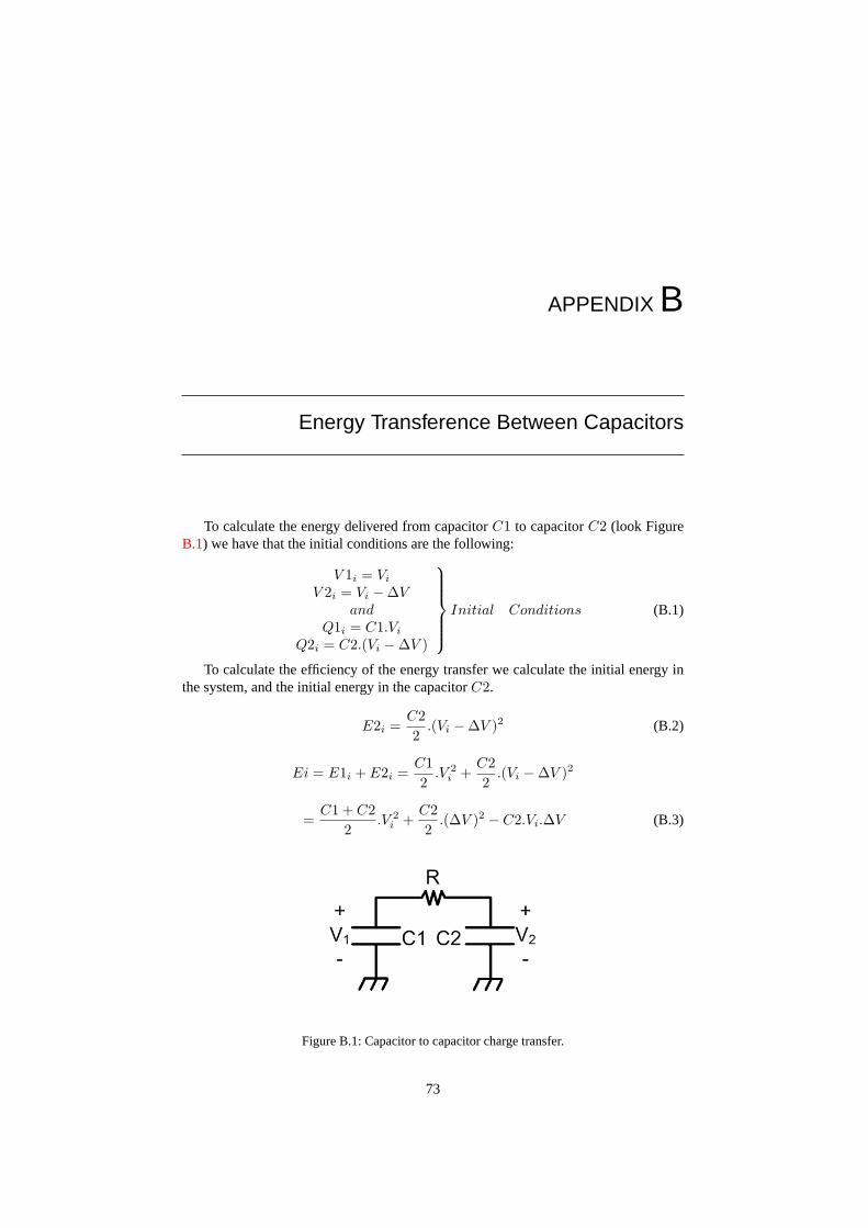
APPENDIX B
Energy Transference Between Capacitors
To calculate the energy delivered from capacitorC1 to capacitorC2 (look FigureB.1) we have that the initial conditions are the following:
V 1i = Vi
V 2i = Vi −∆Vand
Q1i = C1.Vi
Q2i = C2.(Vi −∆V )
Initial Conditions (B.1)
To calculate the efficiency of the energy transfer we calculate the initial energy inthe system, and the initial energy in the capacitorC2.
E2i =C22
.(Vi −∆V )2 (B.2)
Ei = E1i + E2i =C12
.V 2i +
C22
.(Vi −∆V )2
=C1 + C2
2.V 2
i +C22
.(∆V )2 − C2.Vi.∆V (B.3)
Figure B.1: Capacitor to capacitor charge transfer.
73

As the final state is when the voltage is the same inC1 andC2 we have that:
V 1f = V 2f = Vf =Q1f
C1=
Q2f
C2⇒ Q2f =
C2C1
.Q1f (B.4)
And the charge in the system is the same:
Q1f + Q2f = Q1i + Q2i (B.5)
So from (B.1), (B.4) and (B.5):
Q1f = (C1.Vi + C2.(Vi −∆V )).(
C1C1 + C2
)(B.6)
And the final voltage in both capacitors is:
Vf =Q1f
C1= (C1.Vi +C2.(Vi−∆V )).
(1
C1 + C2
)= Vi−
C2C1 + C2
.∆V (B.7)
Then, the final stored energy in the system is:
Ef = E1f + E2f =C12
.V 2f +
C22
.V 2f =
C1 + C22
.V 2f
Ef =C1 + C2
2.
(Vi −
C2C1 + C2
.∆V
)2
Ef =C1 + C2
2.
(V 2
i − 2.C2
C1 + C2.Vi.∆V +
(C2
C1 + C2.∆V
)2)
Ef =C1 + C2
2.V 2
i − C2.Vi.∆V +(C2.∆V )2
2.(C1 + C2)(B.8)
To calculate the energy dissipated1 in the process we have from equations (B.3) and(B.8) that:
ELost = ∆E = Ef − Ei = −C1.C2.∆V 2
2.(C1 + C2)(B.9)
Then, the final energy in capacitorC2 is:
∆E2f =C22
.V 2f (B.10)
So from equations (B.2), (B.7) and (B.10):
∆E2 =C1.C2
C1 + C2.
(Vi.∆V − ∆V 2
2.
(C1 + 2.C2C1 + C2
))(B.11)
To calculate the efficiency of delivering energy fromC1 to C2 we have the fo-llowing equation:
1This energy is dissipated in the resistor R (Figure1.2)
74
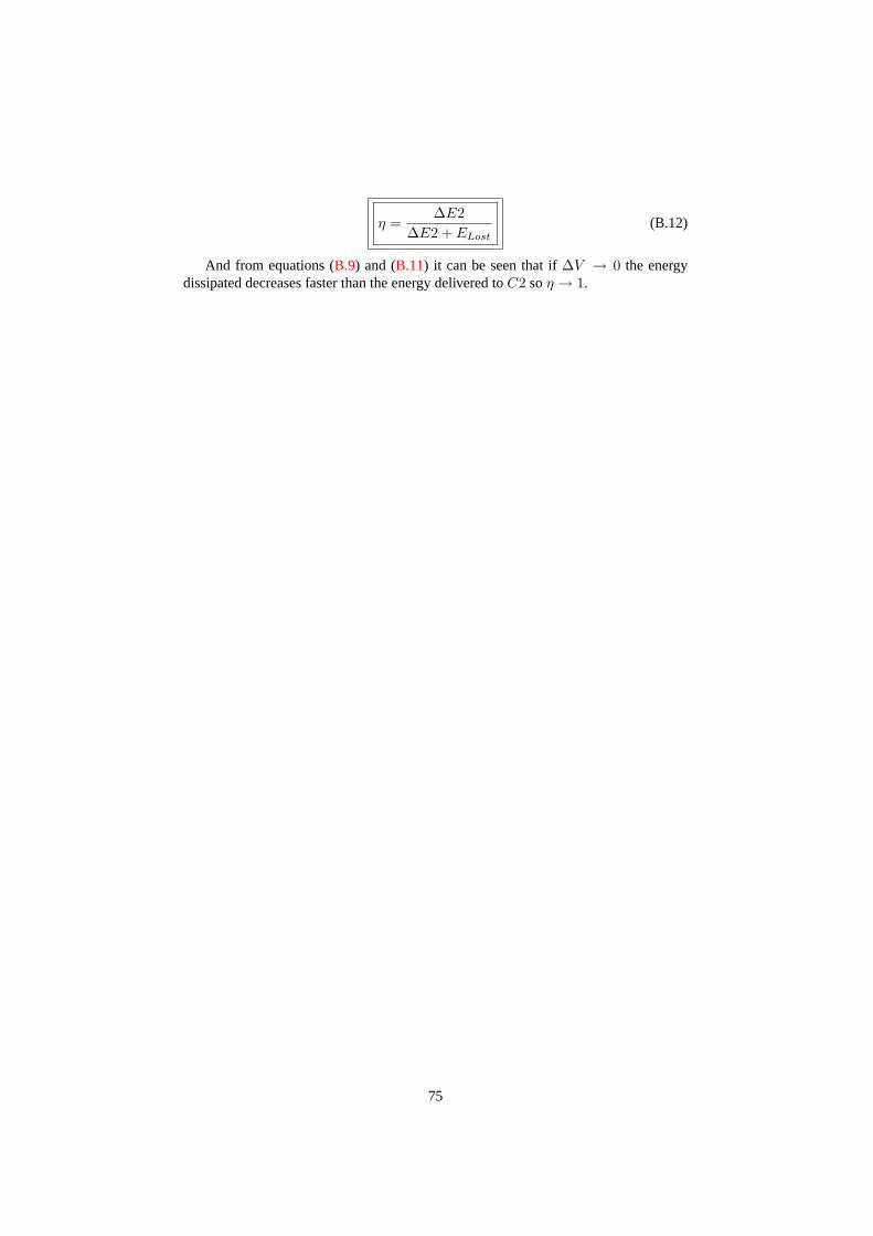
η =∆E2
∆E2 + ELost(B.12)
And from equations (B.9) and (B.11) it can be seen that if∆V → 0 the energydissipated decreases faster than the energy delivered toC2 soη → 1.
75


![Transportemar´ıtimointernacional:aspectosoperativosy ... · aAHCTTUM Quintero-G Ingenier´ıa S.A.S. ... servicios portuarios y mar´ıtimos [1]. Aunque como todos los medios de](https://img.pdfslide.us/doc/110x75/5bd43d5d09d3f214338b99db/transportemaritimointernacionalaspectosoperativosy-aahcttum-quintero-g.jpg)