Embed Size (px)
Citation preview

Freescale Semiconductor Document Number: MMA8652FC
Data Sheet: Technical Data Rev. 3.3, 10/2015An Energy-Efficient Solution by Freescale
MMA8652FC, 3-Axis, 12-bit, Digital AccelerometerThe MMA8652FC is an intelligent, low-power, three-axis, capacitive micromachined accelerometer with 12 bits of resolution. This accelerometer is packed with embedded functions with flexible user-programmable options, configurable to two interrupt pins. Embedded interrupt functions enable overall power savings, by relieving the host processor from continuously polling data. There is access to either low-pass or high-pass filtered data, which minimizes the data analysis required for jolt detection and faster transitions. The device can be configured to generate inertial wake-up interrupt signals from any combination of the configurable embedded functions, enabling the MMA8652FC to monitor inertial events while remaining in a low-power mode during periods of inactivity. The MMA8652FC is available in a small 10-pin DFN package (2 mm x 2 mm x 1 mm).
Features• 1.95 V to 3.6 V supply voltage
• 1.62 V to 3.6 V digital interface voltage
• ±2 g, ±4 g, and ±8 g dynamically selectable full-scale ranges
• Output Data Rates (ODR) from 1.56 Hz to 800 Hz
• 12-bit digital output
• I2C digital output interface with programmable interrupts
• Four embedded channels of configurable motion detection (Freefall, Motion,Pulse, Transient)
• Orientation (Portrait/Landscape) detection with programmable hysteresis
• Configurable automatic ODR change triggered by the Auto-Wake/Sleepstate change
• 32-sample FIFO
• High-Pass Filter Data available per sample and through the FIFO
• Self-Test
Typical applications• Tilt compensation in e-compass applications
• Static orientation detection (Portrait/Landscape, Up/Down, Left/Right, Back/Front position identification)
• Notebook, tablet, e-reader, and laptop tumble and freefall detection
• Real-time orientation detection (virtual reality and gaming 3D user orientation feedback)
• Real-time activity analysis (pedometer step counting, freefall drop detection for HDD, dead-reckoning GPS backup)
• Motion detection for portable product power saving (Auto-SLEEP and Auto-WAKE for cell phone, PDA, GPS, gaming)
• Shock and vibration monitoring (mechatronic compensation, shipping and warranty usage logging)
• User interface (tilt menu scrolling, tap detection for button replacement)
ORDERING INFORMATION
Part Number Temperature Range Package Description Shipping
MMA8652FCR1 -40°C to +85°C DFN-10 Tape and Reel
MMA8652FC
Top View
Pin Connections
VDD
SCL
INT1
BYP
INT2
SDA
GND
GND
VDDIO
GND
1
2
3
4
5
10
9
8
7
6
10-pin DFN2 mm x 2 mm x 1 mmCase 98ASA00301D
Top and Bottom View
Freescale reserves the right to change the detail specifications as may be required to permit improvements in the design of its products.
© 2012–2015 Freescale Semiconductor, Inc. All rights reserved.

Table 1. Feature comparison of the MMA865xFC devices
Feature MMA8652FC MMA8653FC
ADC Resolution (bits) 12 10
Digital Sensitivity in 2 g mode (counts/g) 1024 256
Low-Power Mode Yes Yes
Auto-WAKE Yes Yes
Auto-SLEEP Yes Yes
32-Level FIFO Yes No
Low-Pass Filter Yes Yes
High-Pass Filter Yes No
Transient Detection with High-Pass Filter Yes No
Fixed Orientation Detection No Yes
Programmable Orientation Detection Yes No
Data-Ready Interrupt Yes Yes
Single-Tap Interrupt Yes No
Double-Tap Interrupt Yes No
Directional Tap Interrupt Yes No
Freefall Interrupt Yes Yes
Motion Interrupt with Direction Yes No
MMA8652FC
Sensors2 Freescale Semiconductor, Inc.

Contents1 Block Diagram and Pin Descriptions . . . . . . . . . . . . . . . . . . . . . . . . . . . . . . . . . . . . . . . . . . . . . . . . . . . . . . . . . . . . . . . . 5
1.1 Block diagram . . . . . . . . . . . . . . . . . . . . . . . . . . . . . . . . . . . . . . . . . . . . . . . . . . . . . . . . . . . . . . . . . . . . . . . . . . . . . . . 51.2 Pin descriptions. . . . . . . . . . . . . . . . . . . . . . . . . . . . . . . . . . . . . . . . . . . . . . . . . . . . . . . . . . . . . . . . . . . . . . . . . . . . . . 61.3 Typical application circuit . . . . . . . . . . . . . . . . . . . . . . . . . . . . . . . . . . . . . . . . . . . . . . . . . . . . . . . . . . . . . . . . . . . . . . 6
2 Mechanical and Electrical Specifications. . . . . . . . . . . . . . . . . . . . . . . . . . . . . . . . . . . . . . . . . . . . . . . . . . . . . . . . . . . . . 72.1 Absolute maximum ratings . . . . . . . . . . . . . . . . . . . . . . . . . . . . . . . . . . . . . . . . . . . . . . . . . . . . . . . . . . . . . . . . . . . . . 72.2 Mechanical characteristics . . . . . . . . . . . . . . . . . . . . . . . . . . . . . . . . . . . . . . . . . . . . . . . . . . . . . . . . . . . . . . . . . . . . . 82.3 Electrical characteristics . . . . . . . . . . . . . . . . . . . . . . . . . . . . . . . . . . . . . . . . . . . . . . . . . . . . . . . . . . . . . . . . . . . . . . . 92.4 I2C interface characteristic . . . . . . . . . . . . . . . . . . . . . . . . . . . . . . . . . . . . . . . . . . . . . . . . . . . . . . . . . . . . . . . . . . . . 10
3 Terminology . . . . . . . . . . . . . . . . . . . . . . . . . . . . . . . . . . . . . . . . . . . . . . . . . . . . . . . . . . . . . . . . . . . . . . . . . . . . . . . . . . . 113.1 Sensitivity . . . . . . . . . . . . . . . . . . . . . . . . . . . . . . . . . . . . . . . . . . . . . . . . . . . . . . . . . . . . . . . . . . . . . . . . . . . . . . . . . 113.2 Zero-g offset . . . . . . . . . . . . . . . . . . . . . . . . . . . . . . . . . . . . . . . . . . . . . . . . . . . . . . . . . . . . . . . . . . . . . . . . . . . . . . . 113.3 Self-Test . . . . . . . . . . . . . . . . . . . . . . . . . . . . . . . . . . . . . . . . . . . . . . . . . . . . . . . . . . . . . . . . . . . . . . . . . . . . . . . . . . 11
4 Modes of Operation . . . . . . . . . . . . . . . . . . . . . . . . . . . . . . . . . . . . . . . . . . . . . . . . . . . . . . . . . . . . . . . . . . . . . . . . . . . . . 125 Functionality . . . . . . . . . . . . . . . . . . . . . . . . . . . . . . . . . . . . . . . . . . . . . . . . . . . . . . . . . . . . . . . . . . . . . . . . . . . . . . . . . . . 13
5.1 Device calibration . . . . . . . . . . . . . . . . . . . . . . . . . . . . . . . . . . . . . . . . . . . . . . . . . . . . . . . . . . . . . . . . . . . . . . . . . . . 135.2 8-bit or 12-bit . . . . . . . . . . . . . . . . . . . . . . . . . . . . . . . . . . . . . . . . . . . . . . . . . . . . . . . . . . . . . . . . . . . . . . . . . . . . . . 135.3 Internal FIFO data buffer. . . . . . . . . . . . . . . . . . . . . . . . . . . . . . . . . . . . . . . . . . . . . . . . . . . . . . . . . . . . . . . . . . . . . . 145.4 Low power modes vs. high resolution modes . . . . . . . . . . . . . . . . . . . . . . . . . . . . . . . . . . . . . . . . . . . . . . . . . . . . . . 145.5 Auto-WAKE/SLEEP mode . . . . . . . . . . . . . . . . . . . . . . . . . . . . . . . . . . . . . . . . . . . . . . . . . . . . . . . . . . . . . . . . . . . . 155.6 Freefall and motion detection . . . . . . . . . . . . . . . . . . . . . . . . . . . . . . . . . . . . . . . . . . . . . . . . . . . . . . . . . . . . . . . . . . 155.7 Transient detection . . . . . . . . . . . . . . . . . . . . . . . . . . . . . . . . . . . . . . . . . . . . . . . . . . . . . . . . . . . . . . . . . . . . . . . . . . 155.8 Tap detection . . . . . . . . . . . . . . . . . . . . . . . . . . . . . . . . . . . . . . . . . . . . . . . . . . . . . . . . . . . . . . . . . . . . . . . . . . . . . . 165.9 Orientation detection. . . . . . . . . . . . . . . . . . . . . . . . . . . . . . . . . . . . . . . . . . . . . . . . . . . . . . . . . . . . . . . . . . . . . . . . . 165.10 Interrupt register configurations . . . . . . . . . . . . . . . . . . . . . . . . . . . . . . . . . . . . . . . . . . . . . . . . . . . . . . . . . . . . . . . . 185.11 Serial I2C interface . . . . . . . . . . . . . . . . . . . . . . . . . . . . . . . . . . . . . . . . . . . . . . . . . . . . . . . . . . . . . . . . . . . . . . . . . . 18
6 Register Descriptions. . . . . . . . . . . . . . . . . . . . . . . . . . . . . . . . . . . . . . . . . . . . . . . . . . . . . . . . . . . . . . . . . . . . . . . . . . . . 216.1 Register address map. . . . . . . . . . . . . . . . . . . . . . . . . . . . . . . . . . . . . . . . . . . . . . . . . . . . . . . . . . . . . . . . . . . . . . . . 216.2 Register bit map . . . . . . . . . . . . . . . . . . . . . . . . . . . . . . . . . . . . . . . . . . . . . . . . . . . . . . . . . . . . . . . . . . . . . . . . . . . . 236.3 Data registers . . . . . . . . . . . . . . . . . . . . . . . . . . . . . . . . . . . . . . . . . . . . . . . . . . . . . . . . . . . . . . . . . . . . . . . . . . . . . . 256.4 FIFO registers . . . . . . . . . . . . . . . . . . . . . . . . . . . . . . . . . . . . . . . . . . . . . . . . . . . . . . . . . . . . . . . . . . . . . . . . . . . . . . 276.5 System status and ID registers . . . . . . . . . . . . . . . . . . . . . . . . . . . . . . . . . . . . . . . . . . . . . . . . . . . . . . . . . . . . . . . . . 296.6 Data configuration registers . . . . . . . . . . . . . . . . . . . . . . . . . . . . . . . . . . . . . . . . . . . . . . . . . . . . . . . . . . . . . . . . . . . 316.7 Portrait/Landscape configuration and status registers . . . . . . . . . . . . . . . . . . . . . . . . . . . . . . . . . . . . . . . . . . . . . . . 336.8 Freefall/Motion configuration and status registers . . . . . . . . . . . . . . . . . . . . . . . . . . . . . . . . . . . . . . . . . . . . . . . . . . 376.9 Transient configuration and status registers . . . . . . . . . . . . . . . . . . . . . . . . . . . . . . . . . . . . . . . . . . . . . . . . . . . . . . . 426.10 Pulse configuration and status registers . . . . . . . . . . . . . . . . . . . . . . . . . . . . . . . . . . . . . . . . . . . . . . . . . . . . . . . . . . 456.11 Auto-WAKE/SLEEP detection. . . . . . . . . . . . . . . . . . . . . . . . . . . . . . . . . . . . . . . . . . . . . . . . . . . . . . . . . . . . . . . . . . 516.12 System and control registers . . . . . . . . . . . . . . . . . . . . . . . . . . . . . . . . . . . . . . . . . . . . . . . . . . . . . . . . . . . . . . . . . . 526.13 Data calibration registers . . . . . . . . . . . . . . . . . . . . . . . . . . . . . . . . . . . . . . . . . . . . . . . . . . . . . . . . . . . . . . . . . . . . . 57
7 Mounting Guidelines . . . . . . . . . . . . . . . . . . . . . . . . . . . . . . . . . . . . . . . . . . . . . . . . . . . . . . . . . . . . . . . . . . . . . . . . . . . . 587.1 Overview of soldering considerations . . . . . . . . . . . . . . . . . . . . . . . . . . . . . . . . . . . . . . . . . . . . . . . . . . . . . . . . . . . . 587.2 Halogen content . . . . . . . . . . . . . . . . . . . . . . . . . . . . . . . . . . . . . . . . . . . . . . . . . . . . . . . . . . . . . . . . . . . . . . . . . . . . 587.3 PCB mounting/soldering recommendations . . . . . . . . . . . . . . . . . . . . . . . . . . . . . . . . . . . . . . . . . . . . . . . . . . . . . . . 58
8 Tape and Reel . . . . . . . . . . . . . . . . . . . . . . . . . . . . . . . . . . . . . . . . . . . . . . . . . . . . . . . . . . . . . . . . . . . . . . . . . . . . . . . . . . 608.1 Tape dimensions. . . . . . . . . . . . . . . . . . . . . . . . . . . . . . . . . . . . . . . . . . . . . . . . . . . . . . . . . . . . . . . . . . . . . . . . . . . . 608.2 Device orientation . . . . . . . . . . . . . . . . . . . . . . . . . . . . . . . . . . . . . . . . . . . . . . . . . . . . . . . . . . . . . . . . . . . . . . . . . . . 60
9 Package Dimensions . . . . . . . . . . . . . . . . . . . . . . . . . . . . . . . . . . . . . . . . . . . . . . . . . . . . . . . . . . . . . . . . . . . . . . . . . . . . 6110 Revision History . . . . . . . . . . . . . . . . . . . . . . . . . . . . . . . . . . . . . . . . . . . . . . . . . . . . . . . . . . . . . . . . . . . . . . . . . . . . . . . . 64
Related DocumentationThe MMA8652FC device features and operations are described in a variety of reference manuals, user guides, and application notes. To find the most-current versions of these documents:
1. Go to the Freescale homepage at:
http://www.freescale.com/
2. In the Keyword search box at the top of the page, enter the device number MMA8652FC.
3. In the Refine Your Result pane on the left, click on the Documentation link.
MMA8652FC
SensorsFreescale Semiconductor, Inc. 3

MMA8652FC
Sensors4 Freescale Semiconductor, Inc.
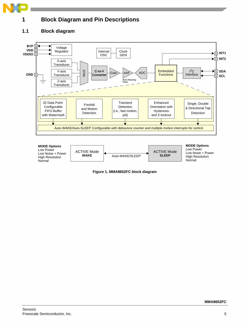
1 Block Diagram and Pin Descriptions
1.1 Block diagram
Figure 1. MMA8652FC block diagram
C-to-VConverter
SDA
SCL
I2CEmbeddedFunctions
C-to-V
InternalOSC
ClockGEN
ADCConverter
VDDIO
GND
X-axisTransducer
Y-axisTransducer
Z-axisTransducer
32 Data Point ConfigurableFIFO Buffer
with Watermark
Freefalland MotionDetection
TransientDetection
(i.e., fast motion,jolt)
EnhancedOrientation with
Hysteresisand Z-lockout
Single, Double
Auto-WAKE/Auto-SLEEP Configurable with debounce counter and multiple motion interrupts for control
Auto-WAKE/SLEEPACTIVE Mode
SLEEP
VDD
& Directional Tap
Detection
INT1
INT2
MODE OptionsLow PowerLow Noise + PowerHigh ResolutionNormal
MODE OptionsLow PowerLow Noise + PowerHigh ResolutionNormal
ACTIVE ModeWAKE
BYP
InterfaceMU
X
VoltageRegulator
Gain AAF
Anti-AliasingFilter
MMA8652FC
SensorsFreescale Semiconductor, Inc. 5
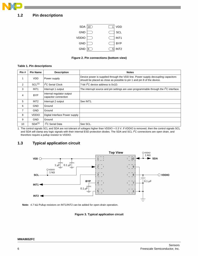
1.2 Pin descriptions
Figure 2. Pin connections (bottom view)
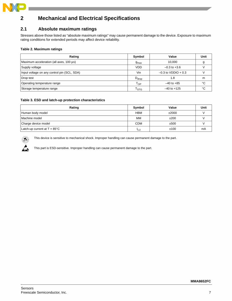
1.3 Typical application circuit
Figure 3. Typical application circuit
Table 1. Pin descriptions
Pin # Pin Name Description Notes
1 VDD Power supplyDevice power is supplied through the VDD line. Power supply decoupling capacitors should be placed as close as possible to pin 1 and pin 8 of the device.
2 SCL(1)
1. The control signals SCL and SDA are not tolerant of voltages higher than VDDIO + 0.3 V. If VDDIO is removed, then the control signals SCL and SDA will clamp any logic signals with their internal ESD protection diodes. The SDA and SCL I2C connections are open drain, and therefore require a pullup resistor to VDDIO.
I2C Serial Clock 7-bit I2C device address is 0x1D.
3 INT1 Interrupt 1 output The interrupt source and pin settings are user-programmable through the I2C interface.
4 BYPInternal regulator output capacitor connection
5 INT2 Interrupt 2 output See INT1.
6 GND Ground
7 GND Ground
8 VDDIO Digital Interface Power supply
9 GND Ground
10 SDA(1) I2C Serial Data See SCL.
1
56
10 VDD
SCL
INT1
BYP
INT2
SDA
GND
VDDIO
GND
GND
VDD
SCL
INT1BYP
INT2
SDA
VDDIO
1
2
10
9
8
7
6
0.1 μF
1 μF
0.1 μF
3
4
5
Top View
VDDIO
VDDIO
1 kΩ
1 kΩ
Note: 4.7 kΩ Pullup resistors on INT1/INT2 can be added for open-drain operation.
0.1 μF
MMA8652FC
Sensors6 Freescale Semiconductor, Inc.
2 Mechanical and Electrical Specifications
2.1 Absolute maximum ratingsStresses above those listed as “absolute maximum ratings” may cause permanent damage to the device. Exposure to maximum rating conditions for extended periods may affect device reliability.
Table 2. Maximum ratings
Rating Symbol Value Unit
Maximum acceleration (all axes, 100 μs) gmax 10,000 g
Supply voltage VDD –0.3 to +3.6 V
Input voltage on any control pin (SCL, SDA) Vin –0.3 to VDDIO + 0.3 V
Drop test Ddrop 1.8 m
Operating temperature range TOP –40 to +85 °C
Storage temperature range TSTG –40 to +125 °C
Table 3. ESD and latch-up protection characteristics
Rating Symbol Value Unit
Human body model HBM ±2000 V
Machine model MM ±200 V
Charge device model CDM ±500 V
Latch-up current at T = 85°C ILU ±100 mA
This device is sensitive to mechanical shock. Improper handling can cause permanent damage to the part.
This part is ESD-sensitive. Improper handling can cause permanent damage to the part.
MMA8652FC
SensorsFreescale Semiconductor, Inc. 7
2.2 Mechanical characteristics
Table 4. Mechanical characteristics at VDD = 2.5 V, VDDIO = 1.8 V, TA = 25°C, unless otherwise noted
Parameter Symbol Test Conditions Min Typ Max Unit
Full-Scale measurement range FS
FS[1:0] set to 00±2 g mode
±2
gFS[1:0] set to 01
±4 g mode±4
FS[1:0] set to 10±8 g mode
±8
Sensitivity So
FS[1:0] set to 00±2 g mode
1024
LSB/gFS[1:0] set to 01
±4 g mode512
FS[1:0] set to 10±8 g mode
256
Sensitivity accuracy Soa ±2.5 %
Sensitivity change vs. temperature TCS –40°C to 85°C ±0.0074 %/°C
Zero-g level offset accuracy (1) TyOff ±25 mg
Zero-g level offset accuracy, post-board mount (2) TyOffPBM ±33.5 mg
Zero-g level change vs. temperature TCO –40°C to 85°C ±0.27 mg/°C
Self-Test output change (±2 g mode) STOC
x +90
LSBy +104
z +782
ODR accuracy ODRa ±3.1 %
Output data bandwidth BW ODR/3 ODR/2 Hz
Output noise RMS Normal mode ODR = 400 Hz 182 µg/√Hz
Operating temperature range TAGOC –40 85 °C
1. Before board mount.2. Post-board mount offset specifications are based on an 8-layer PCB, relative to 25°C.
MMA8652FC
Sensors8 Freescale Semiconductor, Inc.
2.3 Electrical characteristics
Table 5. Electrical characteristics at VDD = 2.5 V, VDDIO = 1.8 V, T = 25°C, unless otherwise noted
Parameter Symbol Test Conditions Min Typ Max Unit
Supply voltage VDD 1.95 2.5 3.6 V
Interface supply voltage VDDIO 1.62 1.8 3.6 V
Low Power mode IddLP
ODR = 1.563 Hz 6.5
μA
ODR = 6.25 Hz 6.5
ODR = 12.5 Hz 6.5
ODR = 50 Hz 15
ODR = 100 Hz 26
ODR = 200 Hz 49
ODR = 400 Hz 94
ODR = 800 Hz 184
Normal mode Idd
ODR = 1.563 Hz 27
μA
ODR = 6.25 Hz 27
ODR = 12.5 Hz 27
ODR = 50 Hz 27
ODR = 100 Hz 49
ODR = 200 Hz 94
ODR = 400 Hz 184
ODR = 800 Hz 184
Boot-Up current IddBoot
VDD = 2.5 V, the current during the Boot sequence is integrated
over 0.5 ms, using a recommended bypass cap
1 mA
Value of capacitor on BYP pin Cap –40°C to 85°C 75 100 470 nF
Standby current IddStby 25°C 1.4 5 μA
Digital high-level input voltage SCL, SDA VIH VDD = 3.6 V, VDDIO = 3.6 V 0.7*VDDIO
V
Digital low-level input voltage SCL, SDA VIL VDD = 1.95 V, VDDIO = 1.62 V 0.3*VDDIO
V
High-level output voltage INT1, INT2 VOH VDD = 3.6 V, VDDIO = 3.6 V,
IO = 500 μA0.9*VDDIO V
Low-level output voltage INT1, INT2 VOL VDD = 1.95 V, VDDIO = 1.62 V,
IO = 500 μA0.1*VDDIO V
Low-level output voltage SDA VOLS IO = 3 mA 0.4
V
Output source current INT1, INT2 IsourceVoltage high level
VOUT = 0.9 x VDDIO2 mA
Output sink current INT1, INT2 IsinkVoltage high level
VOUT = 0.9 x VDDIO3 mA
Power-on ramp time Tpr 0.001 1000 ms
Boot time Tbt
Time from VDDIO on and VDD > VDD min until I2C is
ready for operation, Cbyp = 100 nf
350 500 µs
Turn-on time Ton1Time to obtain valid data from Standby mode to Active mode
2/ODR + 1 ms -
Turn-on time Ton2Time to obtain valid data from
valid voltage applied2/ODR + 2 ms -
Operating temperature range TAGOC –40 85 °C
MMA8652FC
SensorsFreescale Semiconductor, Inc. 9
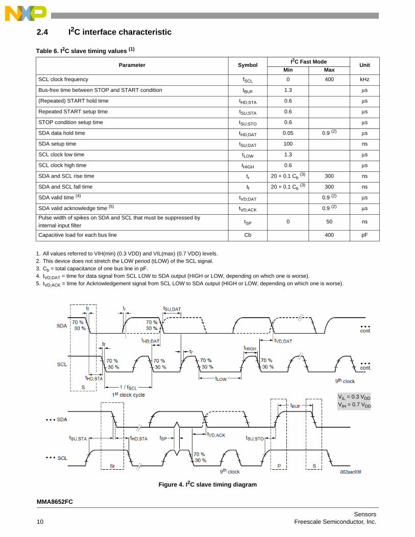
2.4 I2C interface characteristic
Figure 4. I2C slave timing diagram
Table 6. I2C slave timing values (1)
1. All values referred to VIH(min) (0.3 VDD) and VIL(max) (0.7 VDD) levels.
Parameter SymbolI2C Fast Mode
UnitMin Max
SCL clock frequency fSCL 0 400 kHz
Bus-free time between STOP and START condition tBUF 1.3 μs
(Repeated) START hold time tHD;STA 0.6 μs
Repeated START setup time tSU;STA 0.6 μs
STOP condition setup time tSU;STO 0.6 μs
SDA data hold time tHD;DAT 0.05 0.9 (2)
2. This device does not stretch the LOW period (tLOW) of the SCL signal.
μs
SDA setup time tSU;DAT 100 ns
SCL clock low time tLOW 1.3 μs
SCL clock high time tHIGH 0.6 μs
SDA and SCL rise time tr 20 + 0.1 Cb (3)
3. Cb = total capacitance of one bus line in pF.
300 ns
SDA and SCL fall time tf 20 + 0.1 Cb (3) 300 ns
SDA valid time (4)
4. tVD;DAT = time for data signal from SCL LOW to SDA output (HIGH or LOW, depending on which one is worse).
tVD;DAT 0.9 (2) μs
SDA valid acknowledge time (5)
5. tVD;ACK = time for Acknowledgement signal from SCL LOW to SDA output (HIGH or LOW, depending on which one is worse).
tVD;ACK 0.9 (2) μs
Pulse width of spikes on SDA and SCL that must be suppressed by
internal input filtertSP 0 50 ns
Capacitive load for each bus line Cb 400 pF
VIL = 0.3 VDD
VIH = 0.7 VDD
MMA8652FC
Sensors10 Freescale Semiconductor, Inc.

3 Terminology
3.1 SensitivityThe sensitivity is represented in counts/g.
• In ±2 g mode, sensitivity = 1024counts/g.
• In ±4 g mode, sensitivity = 512counts/g.
• In ±8 g mode, sensitivity = 256counts/g.
3.2 Zero-g offsetZero-g Offset (TyOff) describes the deviation of an actual output signal from the ideal output signal if the sensor is stationary. A sensor stationary on a horizontal surface will measure 0 g in X-axis and 0 g in Y-axis, whereas the Z-axis will measure 1 g. The output is ideally in the middle of the dynamic range of the sensor (content of OUT Registers 0x00, data expressed as a 2's complement number). A deviation from ideal value in this case is called Zero-g offset.
Offset is to some extent a result of stress on the MEMS sensor, and therefore the offset can slightly change after mounting the sensor onto a printed circuit board or after exposing it to extensive mechanical stress.
3.3 Self-TestSelf-Test can be used to verify the transducer and signal chain functionality without the need to apply external mechanical stimulus.
When Self-Test is activated:
• An electrostatic actuation force is applied to the sensor, simulating a small acceleration. In this case, the sensor outputs will exhibit a change in their DC levels which, are related to the selected full scale through the device sensitivity.
• The device output level is given by the algebraic sum of the signals produced by the acceleration acting on the sensor and by the electrostatic test-force.
MMA8652FC
SensorsFreescale Semiconductor, Inc. 11
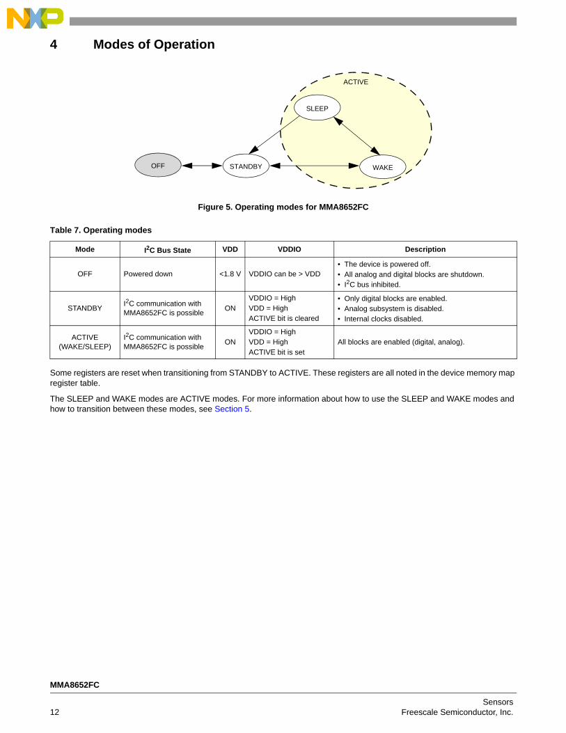
4 Modes of Operation
Figure 5. Operating modes for MMA8652FC
Some registers are reset when transitioning from STANDBY to ACTIVE. These registers are all noted in the device memory map register table.
The SLEEP and WAKE modes are ACTIVE modes. For more information about how to use the SLEEP and WAKE modes and how to transition between these modes, see Section 5.
Table 7. Operating modes
Mode I2C Bus State VDD VDDIO Description
OFF Powered down <1.8 V VDDIO can be > VDD• The device is powered off. • All analog and digital blocks are shutdown. • I2C bus inhibited.
STANDBYI2C communication with MMA8652FC is possible
ONVDDIO = HighVDD = HighACTIVE bit is cleared
• Only digital blocks are enabled.• Analog subsystem is disabled. • Internal clocks disabled.
ACTIVE(WAKE/SLEEP)
I2C communication with MMA8652FC is possible
ONVDDIO = HighVDD = HighACTIVE bit is set
All blocks are enabled (digital, analog).
SLEEP
WAKESTANDBYOFF
ACTIVE
MMA8652FC
Sensors12 Freescale Semiconductor, Inc.

5 FunctionalityThe MMA8652FC is a low-power, digital output 3-axis linear accelerometer with a I2C interface with embedded logic used to detect events and notify an external microprocessor over interrupt lines.
• 8-bit or 12-bit data, high-pass filtered data, 8-bit or 12-bit configurable 32-sample FIFO
• Four different oversampling options that allow for the optimum resolution vs. current consumption trade-off to be made for a given application
• Low-power and auto-WAKE/SLEEP modes for reducing current consumption
• Single/double tap with directional information (one channel)
• Motion detection with directional information or Freefall (one channel)
• Transient/jolt detection based on a high-pass filter, with a settable threshold for detecting the change in acceleration above a threshold with directional information (one channel)
• Flexible user-configurable portrait landscape detection algorithm, for addressing screen orientation
• Two independent interrupt output pins that are programmable among seven interrupt sources (Data Ready, Motion/Freefall, Tap, Orientation, Transient, FIFO, Auto-WAKE)
All functionality is available in ±2 g, ±4 g or ±8 g dynamic measurement ranges. There are many configuration settings for enabling all of the different functions. Separate application notes are available to help configure the device for each embedded functionality.
5.1 Device calibrationThe device is factory calibrated for sensitivity and Zero-g offset for each axis. The trim values are stored in Non-Volatile Memory (NVM). On power-up, the trim parameters are read from NVM and applied to the circuitry. In normal use, further calibration in the end application is not necessary. However, the MMA8652FC allows you to adjust the offset for each axis after power-up, by changing the default offset values. The user offset adjustments are stored in three volatile 8-bit registers (OFF_X, OFF_Y, OFF_Z).
5.2 8-bit or 12-bit The measured acceleration data is stored in the following registers as 2’s complement 12-bit:
• OUT_X_MSB, OUT_X_LSB
• OUT_Y_MSB, OUT_Y_LSB
• OUT_Z_MSB, OUT_Z_LSB
The most significant eight bits of each axis are stored in OUT_X (Y, Z)_MSB, so applications needing only 8-bit results can use these three registers (and ignore the OUT_X/Y/Z_LSB registers). To use only 8-bit results, the F_READ bit in CTRL_REG1 must be set. When the F_READ bit is cleared, the fast read mode is disabled.
• When the full-scale is set to ±2 g, the measurement range is –2 g to +1.999 g, and each count corresponds to (1/1024) g (0.98 mg) at 12-bit resolution.
• When the full-scale is set to ±4 g, the measurement range is –4 g to +3.998 g, and each count corresponds to (1/512) g
• (1.96 mg) at 12-bit resolution.
• When the full-scale is set to ±8 g, the measurement range is –8 g to +7.996 g, and each count corresponds to (1/256) g (3.9 mg) at 12-bit resolution.
• If only the 8-bit results are used, then the resolution is reduced by a factor of 16.
For more information about the data manipulation between data formats and modes, see application note AN4083, Data Manipulation and Basic Settings for Xtrinsic MMA865xFC Accelerometers. There is a device driver available that can be used with the Sensor Toolbox demo board (LFSTBEB865xFC) with this application note.
Table 8. Accelerometer 12-bit output data
12-bit data Range ±2 g (1 mg/LSB) Range ±4 g (2 mg/LSB) Range ±8 g (4 mg/LSB)
0111 1111 1111 1.999 g +3.998 g +7.996 g
0111 1111 1110 1.998 g +3.996 g +7.992 g
… … … …
0000 0000 0001 0.001 g +0.002 g +0.004 g
0000 0000 0000 0.0000 g 0.0000 g 0.0000 g
1111 1111 1111 –0.001 g –0.002 g –0.004 g
MMA8652FC
SensorsFreescale Semiconductor, Inc. 13
5.3 Internal FIFO data bufferMMA8652FC contains a 32-sample internal FIFO data buffer, which helps minimize traffic across the I2C bus. The FIFO can also save system power, by allowing the host processor/MCU to go into a SLEEP mode while the accelerometer independently stores the data (up to 32 samples per axis).
The FIFO can run at all output data rates. There are options for accessing the full 12-bit data or for accessing only the 8-bit data. When access speed is more important than high resolution, the 8-bit data read is a better option.
The FIFO contains four modes (Fill Buffer mode, Circular Buffer mode, Trigger mode, and Disabled mode), which are described in F_SETUP Register 0x09.
• Fill Buffer mode collects the first 32 samples and asserts the overflow flag when the buffer is full and another sample arrives. It does not collect any more data until the buffer is read. This benefits data logging applications where all samples must be collected.
• Circular Buffer mode allows the buffer to be filled and then new data replaces the oldest sample in the buffer. The most recent 32 samples will be stored in the buffer. This benefits situations where the processor is waiting for an specific interrupt to signal that the data must be flushed to analyze the event.
• Trigger mode will hold the last data up to the point when the trigger occurs, and can be set to keep a selectable number of samples after the event occurs.
The MMA8652FC FIFO Buffer has a configurable watermark, allowing the processor to be triggered after a configurable number of samples has filled in the buffer (1 to 32).
5.4 Low power modes vs. high resolution modesThe MMA8652FC can be optimized for lower power modes or for higher resolution of the output data. One of the oversampling schemes of the data can be activated when MODS = 10 in Register 0x2B, which will improve the resolution of the output data only. The highest resolution is achieved at 1.56 Hz.
There is a trade-off between low power and high resolution. Low power can be achieved when the oversampling rate is reduced. When MODS = 11, the lowest power is achieved. The lowest power is achieved when the sample rate is set to 1.56 Hz.
… … … …
1000 0000 0001 –1.999 g –3.998 g –7.996 g
1000 0000 0000 –2.0000 g –4.0000 g –8.0000 g
Table 9. Accelerometer 8-bit output data
8-bit DataRange ±2 g
(15.6 mg/LSB)Range ±4 g
(31.25 mg/LSB)Range ±8 g
(62.5 mg/LSB)
0111 1111 1.9844 g +3.9688 g +7.9375 g
0111 1110 1.9688 g +3.9375 g +7.8750 g
… … … …
0000 0001 +0.0156 g +0.0313 g +0.0625 g
0000 0000 0.000 g 0.0000 g 0.0000 g
1111 1111 –0.0156 g –0.0313 g –0.0625 g
… … … …
1000 0001 –1.9844 g –3.9688 g –7.9375 g
1000 0000 –2.0000 g –4.0000 g –8.0000 g
Table 8. Accelerometer 12-bit output data (Continued)
12-bit data Range ±2 g (1 mg/LSB) Range ±4 g (2 mg/LSB) Range ±8 g (4 mg/LSB)
MMA8652FC
Sensors14 Freescale Semiconductor, Inc.
5.5 Auto-WAKE/SLEEP modeThe MMA8652FC can be configured to transition between sample rates (with their respective current consumption) based on four of the interrupt functions of the device. The advantage of using the Auto-WAKE/SLEEP is that the system can automatically transition to a higher sample rate (higher current consumption) when needed, but spends the majority of the time in the SLEEP mode (lower current) when the device does not require higher sampling rates.
• Auto-WAKE refers to the device being triggered by one of the interrupt functions to transition to a higher sample rate. This may also interrupt the processor to transition from a SLEEP mode to a higher power mode.
• SLEEP mode occurs after the accelerometer has not detected an interrupt for longer than the user-definable timeout period. The device will transition to the specified lower sample rate. It may also alert the processor to go into a lower power mode, to save on current during this period of inactivity.
The Interrupts that can WAKE the device from SLEEP are the following: Tap Detection, Orientation Detection, Motion/Freefall, and Transient Detection. The FIFO can be configured to hold the data in the buffer until it is flushed, if the FIFO Gate bit is set (in Register 0x2C) and if the FIFO cannot WAKE the device from SLEEP.
The interrupts that can keep the device from falling asleep are the same interrupts that can wake the device—with the addition of the FIFO. If the FIFO interrupt is enabled and data is being accessed continually servicing the interrupt, then the device will remain in WAKE mode.
5.6 Freefall and motion detectionMMA8652FC has a flexible interrupt architecture for detecting either a Freefall or a Motion.
• Freefall can be enabled where the set threshold must be less than the configured threshold.
• Motion can be enabled where the set threshold must be greater than the configured threshold.
The motion configuration has the option of enabling or disabling a high-pass filter to eliminate tilt data (static offset); the freefall configuration does not use the high-pass filter.
5.6.1 Freefall detection
The detection of “Freefall” involves the monitoring of the X, Y, and Z axes for the condition where the acceleration magnitude is below a user-specified threshold for a user-definable amount of time. Usable threshold levels are typically between ±100 mg and ±500 mg.
5.6.2 Motion detection
Motion is often used to simply alert the main processor that the device is currently in use. When the acceleration exceeds a set threshold, the motion interrupt is asserted. A motion can be a fast moving shake or a slow moving tilt. This will depend on the threshold and timing values configured for the event.
• The motion detection function can analyze static acceleration changes or faster jolts. For example, to detect that an object is spinning, all three axes would be enabled with a threshold detection of > 2 g. This condition would need to occur for a minimum of 100 ms to ensure that the event was not just noise. The timing value is set by a configurable debounce counter. The debounce counter acts like a filter to determine whether the condition exists for configurable set of time (like 100 ms or longer).
• To detect the direction of the motion, there is also directional data available in the source register. This is useful for applications such as directional shake or flick, which assists with the algorithm for various gesture detections.
5.7 Transient detectionThe MMA8652FC has a built-in, high-pass filter. Acceleration data goes through the high pass filter, eliminating the offset (DC) and low frequencies. The high-pass filter cutoff frequency can be set to four different frequencies, which depends on the Output Data Rate (ODR). A higher cutoff frequency ensures that the DC data (or slower moving data) will be filtered out, allowing only the higher frequencies to pass. The embedded transient detection function uses the high-pass filtered data, allowing you to set the threshold and debounce counter. The transient detection feature can be used in the same manner as the motion detection feature, by bypassing the high-pass filter. There is an option in the configuration register to do this, which adds more flexibility to accommodate various use cases.
Many applications use the accelerometer’s static acceleration readings (like tilt), which measure the change in acceleration due to gravity only. These functions benefit from acceleration data being filtered with a low-pass filter where high frequency data is considered noise. However, there are many functions where the accelerometer must analyze dynamic acceleration. Functions such as tap, flick, shake and step counting are based on the analysis of the change in the acceleration. It is simpler to interpret these functions (which are dependent on dynamic acceleration data) when the static component has been removed.
MMA8652FC
SensorsFreescale Semiconductor, Inc. 15
The Transient Detection function can be routed to either interrupt pin through bit 5 in CTRL_REG5 register (0x2E). Registers 0x1D – 0x20 are the dedicated Transient Detection configuration registers. The source register contains directional data to determine the direction of the acceleration (either positive or negative).
5.8 Tap detectionThe MMA8652FC has embedded single/double and directional tap detection.
• The tap detection function has various customizing timers, for setting the pulse time width and the latency time between pulses. There are programmable thresholds for all three axes.
• The tap detection can be configured to run through the high-pass filter and also through a low-pass filter, which provides more customizing and tunable tap detection schemes.
• The status register provides updates on the axes where the event was detected and the direction of the tap.
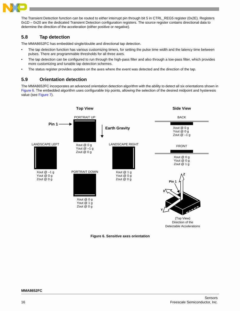
5.9 Orientation detectionThe MMA8652FC incorporates an advanced orientation detection algorithm with the ability to detect all six orientations shown in Figure 6. The embedded algorithm uses configurable trip points, allowing the selection of the desired midpoint and hysteresis value (see Figure 7).
Figure 6. Sensitive axes orientation
Top View
PORTRAIT UP
Earth GravityPin 1
Xout @ 0 gYout @ –1 gZout @ 0 g
Xout @ 1 gYout @ 0 gZout @ 0 g
Xout @ 0 gYout @ 1 gZout @ 0 g
Xout @ –1 gYout @ 0 gZout @ 0 g
LANDSCAPE LEFT
PORTRAIT DOWN
LANDSCAPE RIGHT
Side View
FRONT
Xout @ 0 gYout @ 0 gZout @ 1 g
BACK
Xout @ 0 gYout @ 0 gZout @ –1 g
X
Y
Z
Pin 1
(Top View)Direction of the
Detectable Accelerations
MMA8652FC
Sensors16 Freescale Semiconductor, Inc.
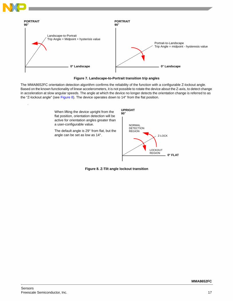
Figure 7. Landscape-to-Portrait transition trip angles
The MMA8652FC orientation detection algorithm confirms the reliability of the function with a configurable Z-lockout angle. Based on the known functionality of linear accelerometers, it is not possible to rotate the device about the Z-axis, to detect change in acceleration at slow angular speeds. The angle at which the device no longer detects the orientation change is referred to as the “Z-lockout angle” (see Figure 8). The device operates down to 14° from the flat position.
.
Figure 8. Z-Tilt angle lockout transition
PORTRAIT
Landscape-to-Portrait
90°
Trip Angle = Midpoint + hysterisis value
0° Landscape
PORTRAIT
Portrait-to-Landscape
90°
Trip Angle = midpoint - hysteresis value
0° Landscape
UPRIGHT
NORMAL
90°
Z-LOCK
0° FLAT
DETECTIONREGION
LOCKOUTREGION
When lifting the device upright from the flat position, orientation detection will be active for orientation angles greater than a user-configurable value.
The default angle is 29° from flat, but the angle can be set as low as 14°.
MMA8652FC
SensorsFreescale Semiconductor, Inc. 17
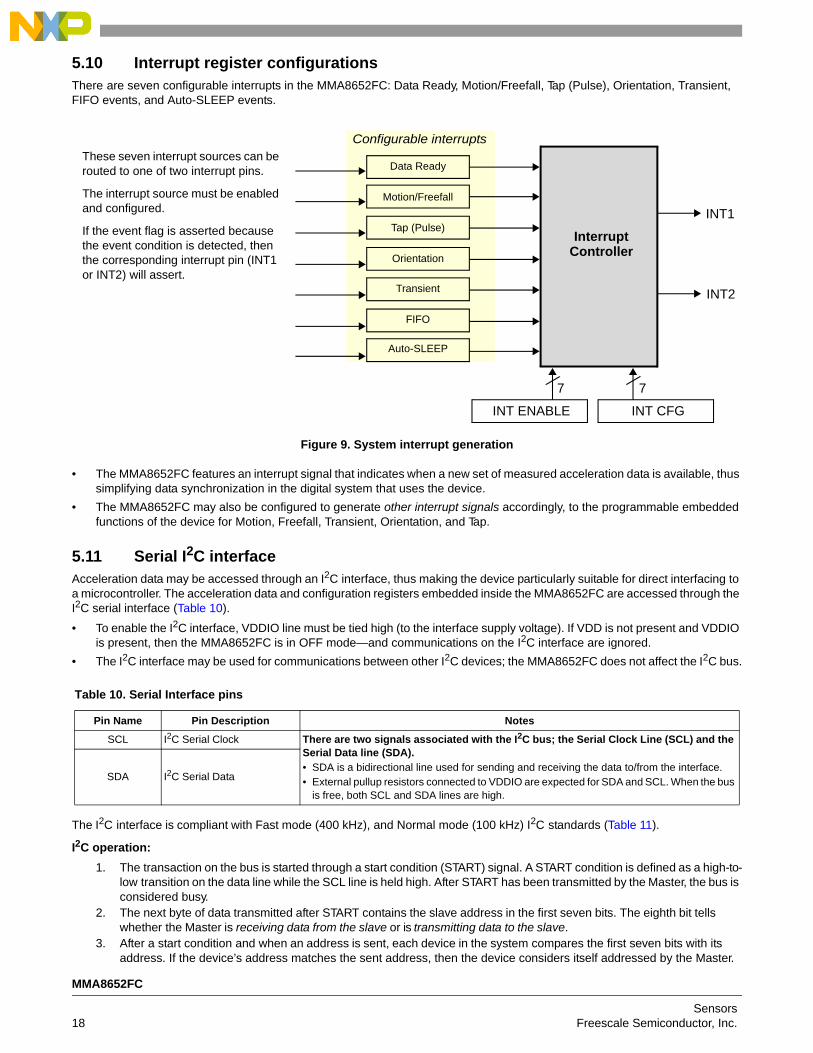
5.10 Interrupt register configurationsThere are seven configurable interrupts in the MMA8652FC: Data Ready, Motion/Freefall, Tap (Pulse), Orientation, Transient, FIFO events, and Auto-SLEEP events.
Figure 9. System interrupt generation
• The MMA8652FC features an interrupt signal that indicates when a new set of measured acceleration data is available, thus simplifying data synchronization in the digital system that uses the device.
• The MMA8652FC may also be configured to generate other interrupt signals accordingly, to the programmable embedded functions of the device for Motion, Freefall, Transient, Orientation, and Tap.
5.11 Serial I2C interfaceAcceleration data may be accessed through an I2C interface, thus making the device particularly suitable for direct interfacing to a microcontroller. The acceleration data and configuration registers embedded inside the MMA8652FC are accessed through the I2C serial interface (Table 10).
• To enable the I2C interface, VDDIO line must be tied high (to the interface supply voltage). If VDD is not present and VDDIO is present, then the MMA8652FC is in OFF mode—and communications on the I2C interface are ignored.
• The I2C interface may be used for communications between other I2C devices; the MMA8652FC does not affect the I2C bus.
The I2C interface is compliant with Fast mode (400 kHz), and Normal mode (100 kHz) I2C standards (Table 11).
I2C operation:
1. The transaction on the bus is started through a start condition (START) signal. A START condition is defined as a high-to-low transition on the data line while the SCL line is held high. After START has been transmitted by the Master, the bus is considered busy.
2. The next byte of data transmitted after START contains the slave address in the first seven bits. The eighth bit tells whether the Master is receiving data from the slave or is transmitting data to the slave.
3. After a start condition and when an address is sent, each device in the system compares the first seven bits with its address. If the device’s address matches the sent address, then the device considers itself addressed by the Master.
Table 10. Serial Interface pins
Pin Name Pin Description Notes
SCL I2C Serial Clock There are two signals associated with the I2C bus; the Serial Clock Line (SCL) and the Serial Data line (SDA). • SDA is a bidirectional line used for sending and receiving the data to/from the interface. • External pullup resistors connected to VDDIO are expected for SDA and SCL. When the bus
is free, both SCL and SDA lines are high.
SDA I2C Serial Data
InterruptController
Data Ready
Motion/Freefall
Tap (Pulse)
Orientation
Transient
FIFO
Auto-SLEEP
INT ENABLE INT CFG
INT1
INT2
7 7
Configurable interruptsThese seven interrupt sources can be routed to one of two interrupt pins.
The interrupt source must be enabled and configured.
If the event flag is asserted because the event condition is detected, then the corresponding interrupt pin (INT1 or INT2) will assert.
MMA8652FC
Sensors18 Freescale Semiconductor, Inc.
4. The 9th clock pulse following the slave address byte (and each subsequent byte) is the acknowledge (ACK). The transmitter must release the SDA line during the ACK period. The receiver must then pull the data line low, so that it remains stable low during the high period of the acknowledge clock period.
5. A Master may also issue a repeated START during a data transfer. The MMA8652FC expects repeated STARTs to be used to randomly read from specific registers.
6. A low-to-high transition on the SDA line while the SCL line is high is defined as a stop condition (STOP). A data transfer is always terminated by a STOP.
The MMA8652FC's standard slave address is 0011101 or 0x01D.
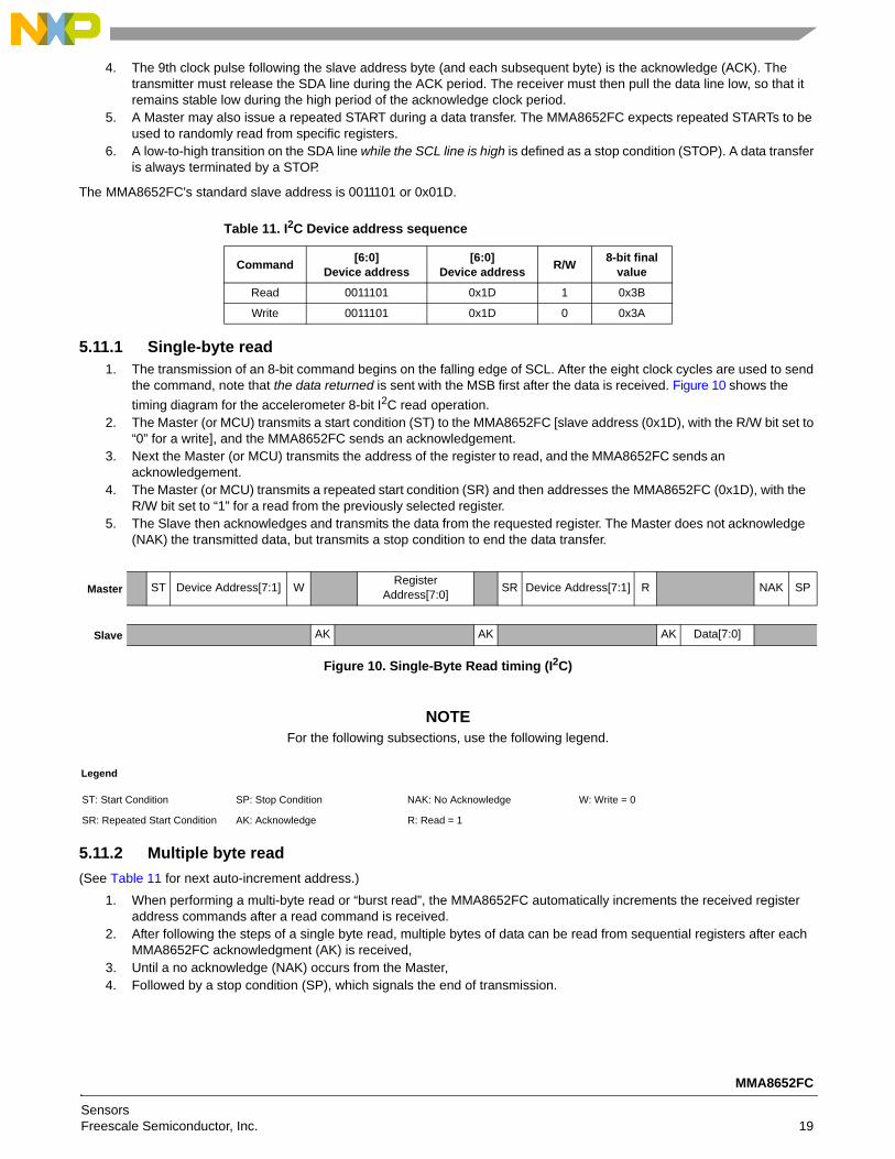
5.11.1 Single-byte read1. The transmission of an 8-bit command begins on the falling edge of SCL. After the eight clock cycles are used to send
the command, note that the data returned is sent with the MSB first after the data is received. Figure 10 shows the
timing diagram for the accelerometer 8-bit I2C read operation. 2. The Master (or MCU) transmits a start condition (ST) to the MMA8652FC [slave address (0x1D), with the R/W bit set to
“0” for a write], and the MMA8652FC sends an acknowledgement. 3. Next the Master (or MCU) transmits the address of the register to read, and the MMA8652FC sends an
acknowledgement. 4. The Master (or MCU) transmits a repeated start condition (SR) and then addresses the MMA8652FC (0x1D), with the
R/W bit set to “1” for a read from the previously selected register. 5. The Slave then acknowledges and transmits the data from the requested register. The Master does not acknowledge
(NAK) the transmitted data, but transmits a stop condition to end the data transfer.
Figure 10. Single-Byte Read timing (I2C)
NOTEFor the following subsections, use the following legend.
5.11.2 Multiple byte read
(See Table 11 for next auto-increment address.)
1. When performing a multi-byte read or “burst read”, the MMA8652FC automatically increments the received register address commands after a read command is received.
2. After following the steps of a single byte read, multiple bytes of data can be read from sequential registers after each MMA8652FC acknowledgment (AK) is received,
3. Until a no acknowledge (NAK) occurs from the Master,4. Followed by a stop condition (SP), which signals the end of transmission.
Table 11. I2C Device address sequence
Command[6:0]
Device address[6:0]
Device addressR/W
8-bit final value
Read 0011101 0x1D 1 0x3B
Write 0011101 0x1D 0 0x3A
Master ST Device Address[7:1] WRegister
Address[7:0]SR Device Address[7:1] R NAK SP
Slave AK AK AK Data[7:0]
Legend
ST: Start Condition SP: Stop Condition NAK: No Acknowledge W: Write = 0
SR: Repeated Start Condition AK: Acknowledge R: Read = 1
MMA8652FC
SensorsFreescale Semiconductor, Inc. 19
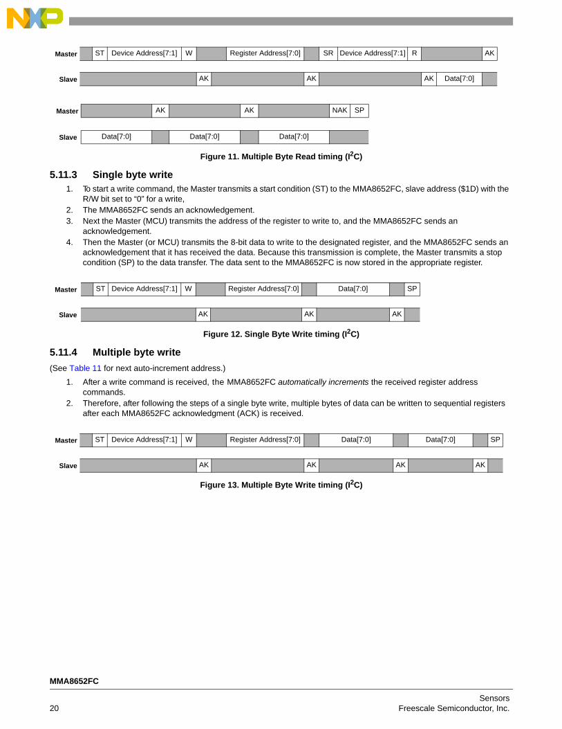
Figure 11. Multiple Byte Read timing (I2C)
5.11.3 Single byte write1. To start a write command, the Master transmits a start condition (ST) to the MMA8652FC, slave address ($1D) with the
R/W bit set to “0” for a write, 2. The MMA8652FC sends an acknowledgement. 3. Next the Master (MCU) transmits the address of the register to write to, and the MMA8652FC sends an
acknowledgement. 4. Then the Master (or MCU) transmits the 8-bit data to write to the designated register, and the MMA8652FC sends an
acknowledgement that it has received the data. Because this transmission is complete, the Master transmits a stop condition (SP) to the data transfer. The data sent to the MMA8652FC is now stored in the appropriate register.
Figure 12. Single Byte Write timing (I2C)
5.11.4 Multiple byte write
(See Table 11 for next auto-increment address.)
1. After a write command is received, the MMA8652FC automatically increments the received register address commands.
2. Therefore, after following the steps of a single byte write, multiple bytes of data can be written to sequential registers after each MMA8652FC acknowledgment (ACK) is received.
Figure 13. Multiple Byte Write timing (I2C)
Master ST Device Address[7:1] W Register Address[7:0] SR Device Address[7:1] R AK
Slave AK AK AK Data[7:0]
Master AK AK NAK SP
Slave Data[7:0] Data[7:0] Data[7:0]
Master ST Device Address[7:1] W Register Address[7:0] Data[7:0] SP
Slave AK AK AK
Master ST Device Address[7:1] W Register Address[7:0] Data[7:0] Data[7:0] SP
Slave AK AK AK AK
MMA8652FC
Sensors20 Freescale Semiconductor, Inc.
6 Register Descriptions
6.1 Register address map
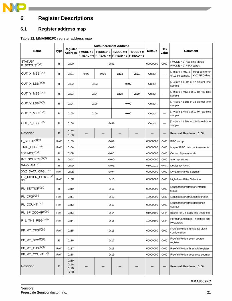
Table 12. MMA8652FC register address map
Name TypeRegisterAddress
Auto-Increment Address
DefaultHex
ValueCommentFMODE = 0
F_READ = 0
FMODE > 0
F_READ = 0
FMODE = 0
F_READ = 1
FMODE > 0
F_READ = 1
STATUS/F_STATUS(1)(2) R 0x00 0x01 00000000 0x00
FMODE = 0, real time status
FMODE > 0, FIFO status
OUT_X_MSB(1)(2) R 0x01 0x02 0x01 0x03 0x01 Output —[7:0] are 8 MSBs
of 12-bit sample.
Root pointer to
XYZ FIFO data.
OUT_X_LSB(1)(2) R 0x02 0x03 0x00 Output —[7:4] are 4 LSBs of 12-bit real-time
sample
OUT_Y_MSB(1)(2) R 0x03 0x04 0x05 0x00 Output —[7:0] are 8 MSBs of 12-bit real-time
sample
OUT_Y_LSB(1)(2) R 0x04 0x05 0x00 Output —[7:4] are 4 LSBs of 12-bit real-time
sample
OUT_Z_MSB(1)(2) R 0x05 0x06 0x00 Output —[7:0] are 8 MSBs of 12-bit real-time
sample
OUT_Z_LSB(1)(2) R 0x06 0x00 Output —[7:4] are 4 LSBs of 12-bit real-time
sample
Reserved R0x07
0x08— — — — — — Reserved. Read return 0x00.
F_SETUP(1)(3) R/W 0x09 0x0A 00000000 0x00 FIFO setup
TRIG_CFG(1)(4) R/W 0x0A 0x0B 00000000 0x00 Map of FIFO data capture events
SYSMOD(1)(2) R 0x0B 0x0C 00000000 0x00 Current System mode
INT_SOURCE(1)(2) R 0x0C 0x0D 00000000 0x00 Interrupt status
WHO_AM_I(1) R 0x0D 0x0E 01001010 0x4A Device ID (0x4A)
XYZ_DATA_CFG(1)(4) R/W 0x0E 0x0F 00000000 0x00 Dynamic Range Settings
HP_FILTER_CUTOFF(1
)(4) R/W 0x0F 0x10 00000000 0x00 High-Pass Filter Selection
PL_STATUS(1)(2) R 0x10 0x11 00000000 0x00Landscape/Portrait orientation
status
PL_CFG(1)(4) R/W 0x11 0x12 10000000 0x80 Landscape/Portrait configuration.
PL_COUNT(1)(3) R/W 0x12 0x13 00000000 0x00Landscape/Portrait debounce
counter
PL_BF_ZCOMP(1)(4) R/W 0x13 0x14 01000100 0x44 Back/Front, Z-Lock Trip threshold
P_L_THS_REG(1)(4) R/W 0x14 0x15 10000100 0x84Portrait/Landscape Threshold and
Hysteresis
FF_MT_CFG(1)(4) R/W 0x15 0x16 00000000 0x00Freefall/Motion functional block
configuration
FF_MT_SRC(1)(2) R 0x16 0x17 00000000 0x00Freefall/Motion event source
register
FF_MT_THS(1)(3) R/W 0x17 0x18 00000000 0x00 Freefall/Motion threshold register
FF_MT_COUNT(1)(3) R/W 0x18 0x19 00000000 0x00 Freefall/Motion debounce counter
Reserved R
0x19
0x1A
0x1B
0x1C
— — — — — — Reserved. Read return 0x00.
MMA8652FC
SensorsFreescale Semiconductor, Inc. 21
NOTEAuto-increment addresses that are not a simple increment are highlighted in bold. The auto-increment addressing is only enabled when device registers are read using I2C burst read mode. The internally stored auto-increment address is cleared whenever an I2C STOP condition is detected.
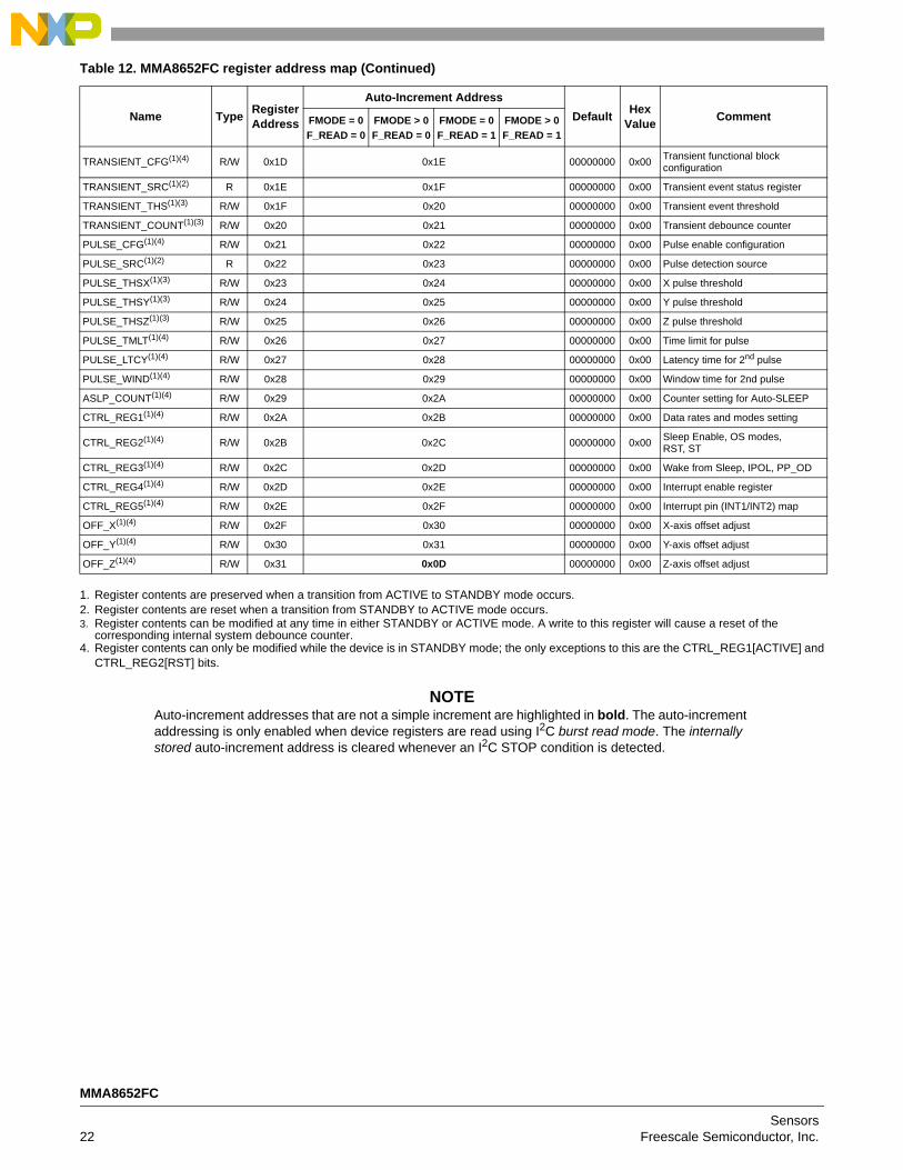
TRANSIENT_CFG(1)(4) R/W 0x1D 0x1E 00000000 0x00Transient functional block configuration
TRANSIENT_SRC(1)(2) R 0x1E 0x1F 00000000 0x00 Transient event status register
TRANSIENT_THS(1)(3) R/W 0x1F 0x20 00000000 0x00 Transient event threshold
TRANSIENT_COUNT(1)(3) R/W 0x20 0x21 00000000 0x00 Transient debounce counter
PULSE_CFG(1)(4) R/W 0x21 0x22 00000000 0x00 Pulse enable configuration
PULSE_SRC(1)(2) R 0x22 0x23 00000000 0x00 Pulse detection source
PULSE_THSX(1)(3) R/W 0x23 0x24 00000000 0x00 X pulse threshold
PULSE_THSY(1)(3) R/W 0x24 0x25 00000000 0x00 Y pulse threshold
PULSE_THSZ(1)(3) R/W 0x25 0x26 00000000 0x00 Z pulse threshold
PULSE_TMLT(1)(4) R/W 0x26 0x27 00000000 0x00 Time limit for pulse
PULSE_LTCY(1)(4) R/W 0x27 0x28 00000000 0x00 Latency time for 2nd pulse
PULSE_WIND(1)(4) R/W 0x28 0x29 00000000 0x00 Window time for 2nd pulse
ASLP_COUNT(1)(4) R/W 0x29 0x2A 00000000 0x00 Counter setting for Auto-SLEEP
CTRL_REG1(1)(4) R/W 0x2A 0x2B 00000000 0x00 Data rates and modes setting
CTRL_REG2(1)(4) R/W 0x2B 0x2C 00000000 0x00Sleep Enable, OS modes,RST, ST
CTRL_REG3(1)(4) R/W 0x2C 0x2D 00000000 0x00 Wake from Sleep, IPOL, PP_OD
CTRL_REG4(1)(4) R/W 0x2D 0x2E 00000000 0x00 Interrupt enable register
CTRL_REG5(1)(4) R/W 0x2E 0x2F 00000000 0x00 Interrupt pin (INT1/INT2) map
OFF_X(1)(4) R/W 0x2F 0x30 00000000 0x00 X-axis offset adjust
OFF_Y(1)(4) R/W 0x30 0x31 00000000 0x00 Y-axis offset adjust
OFF_Z(1)(4) R/W 0x31 0x0D 00000000 0x00 Z-axis offset adjust
1. Register contents are preserved when a transition from ACTIVE to STANDBY mode occurs.2. Register contents are reset when a transition from STANDBY to ACTIVE mode occurs.3. Register contents can be modified at any time in either STANDBY or ACTIVE mode. A write to this register will cause a reset of the
corresponding internal system debounce counter.4. Register contents can only be modified while the device is in STANDBY mode; the only exceptions to this are the CTRL_REG1[ACTIVE] and
CTRL_REG2[RST] bits.
Table 12. MMA8652FC register address map (Continued)
Name TypeRegisterAddress
Auto-Increment Address
DefaultHex
ValueCommentFMODE = 0
F_READ = 0
FMODE > 0
F_READ = 0
FMODE = 0
F_READ = 1
FMODE > 0
F_READ = 1
MMA8652FC
Sensors22 Freescale Semiconductor, Inc.
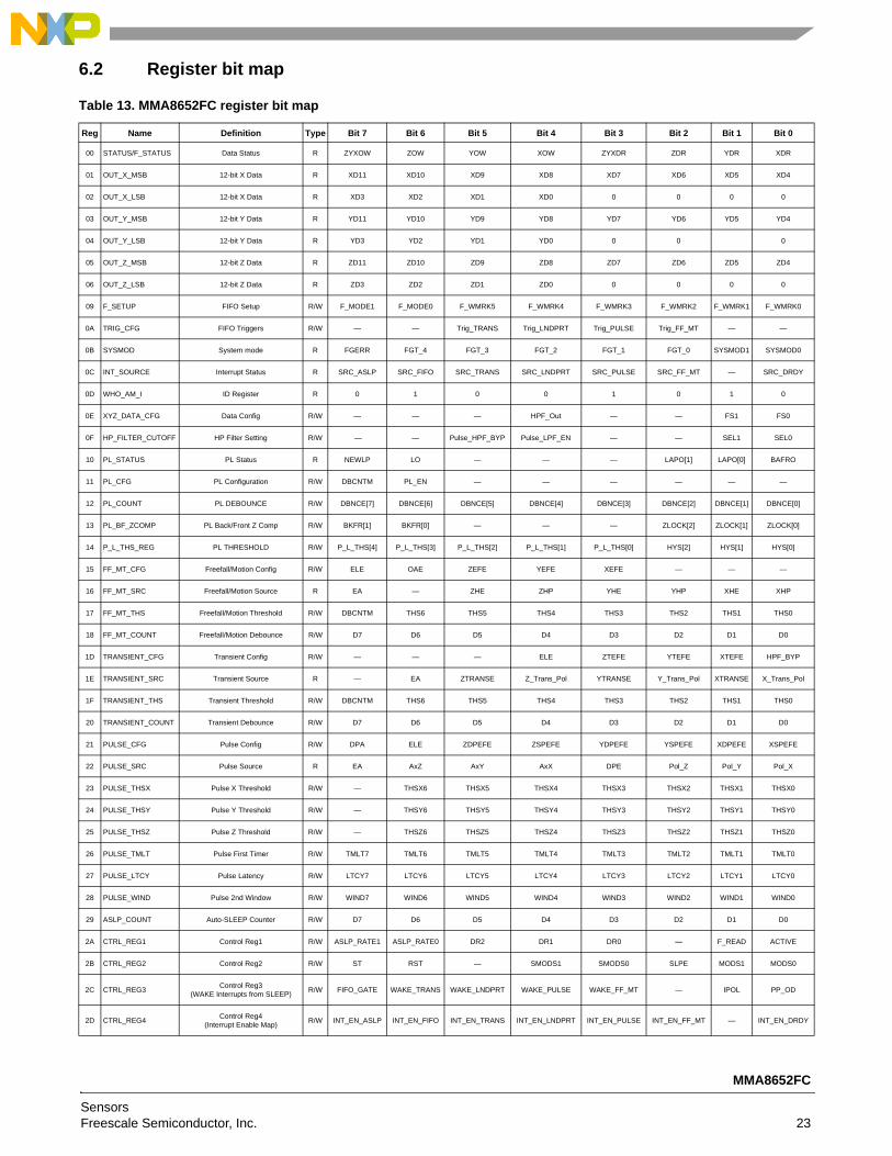
6.2 Register bit map
Table 13. MMA8652FC register bit map
Reg Name Definition Type Bit 7 Bit 6 Bit 5 Bit 4 Bit 3 Bit 2 Bit 1 Bit 0
00 STATUS/F_STATUS Data Status R ZYXOW ZOW YOW XOW ZYXDR ZDR YDR XDR
01 OUT_X_MSB 12-bit X Data R XD11 XD10 XD9 XD8 XD7 XD6 XD5 XD4
02 OUT_X_LSB 12-bit X Data R XD3 XD2 XD1 XD0 0 0 0 0
03 OUT_Y_MSB 12-bit Y Data R YD11 YD10 YD9 YD8 YD7 YD6 YD5 YD4
04 OUT_Y_LSB 12-bit Y Data R YD3 YD2 YD1 YD0 0 0 0
05 OUT_Z_MSB 12-bit Z Data R ZD11 ZD10 ZD9 ZD8 ZD7 ZD6 ZD5 ZD4
06 OUT_Z_LSB 12-bit Z Data R ZD3 ZD2 ZD1 ZD0 0 0 0 0
09 F_SETUP FIFO Setup R/W F_MODE1 F_MODE0 F_WMRK5 F_WMRK4 F_WMRK3 F_WMRK2 F_WMRK1 F_WMRK0
0A TRIG_CFG FIFO Triggers R/W — — Trig_TRANS Trig_LNDPRT Trig_PULSE Trig_FF_MT — —
0B SYSMOD System mode R FGERR FGT_4 FGT_3 FGT_2 FGT_1 FGT_0 SYSMOD1 SYSMOD0
0C INT_SOURCE Interrupt Status R SRC_ASLP SRC_FIFO SRC_TRANS SRC_LNDPRT SRC_PULSE SRC_FF_MT — SRC_DRDY
0D WHO_AM_I ID Register R 0 1 0 0 1 0 1 0
0E XYZ_DATA_CFG Data Config R/W — — — HPF_Out — — FS1 FS0
0F HP_FILTER_CUTOFF HP Filter Setting R/W — — Pulse_HPF_BYP Pulse_LPF_EN — — SEL1 SEL0
10 PL_STATUS PL Status R NEWLP LO — — — LAPO[1] LAPO[0] BAFRO
11 PL_CFG PL Configuration R/W DBCNTM PL_EN — — — — — —
12 PL_COUNT PL DEBOUNCE R/W DBNCE[7] DBNCE[6] DBNCE[5] DBNCE[4] DBNCE[3] DBNCE[2] DBNCE[1] DBNCE[0]
13 PL_BF_ZCOMP PL Back/Front Z Comp R/W BKFR[1] BKFR[0] — — — ZLOCK[2] ZLOCK[1] ZLOCK[0]
14 P_L_THS_REG PL THRESHOLD R/W P_L_THS[4] P_L_THS[3] P_L_THS[2] P_L_THS[1] P_L_THS[0] HYS[2] HYS[1] HYS[0]
15 FF_MT_CFG Freefall/Motion Config R/W ELE OAE ZEFE YEFE XEFE — — —
16 FF_MT_SRC Freefall/Motion Source R EA — ZHE ZHP YHE YHP XHE XHP
17 FF_MT_THS Freefall/Motion Threshold R/W DBCNTM THS6 THS5 THS4 THS3 THS2 THS1 THS0
18 FF_MT_COUNT Freefall/Motion Debounce R/W D7 D6 D5 D4 D3 D2 D1 D0
1D TRANSIENT_CFG Transient Config R/W — — — ELE ZTEFE YTEFE XTEFE HPF_BYP
1E TRANSIENT_SRC Transient Source R — EA ZTRANSE Z_Trans_Pol YTRANSE Y_Trans_Pol XTRANSE X_Trans_Pol
1F TRANSIENT_THS Transient Threshold R/W DBCNTM THS6 THS5 THS4 THS3 THS2 THS1 THS0
20 TRANSIENT_COUNT Transient Debounce R/W D7 D6 D5 D4 D3 D2 D1 D0
21 PULSE_CFG Pulse Config R/W DPA ELE ZDPEFE ZSPEFE YDPEFE YSPEFE XDPEFE XSPEFE
22 PULSE_SRC Pulse Source R EA AxZ AxY AxX DPE Pol_Z Pol_Y Pol_X
23 PULSE_THSX Pulse X Threshold R/W — THSX6 THSX5 THSX4 THSX3 THSX2 THSX1 THSX0
24 PULSE_THSY Pulse Y Threshold R/W — THSY6 THSY5 THSY4 THSY3 THSY2 THSY1 THSY0
25 PULSE_THSZ Pulse Z Threshold R/W — THSZ6 THSZ5 THSZ4 THSZ3 THSZ2 THSZ1 THSZ0
26 PULSE_TMLT Pulse First Timer R/W TMLT7 TMLT6 TMLT5 TMLT4 TMLT3 TMLT2 TMLT1 TMLT0
27 PULSE_LTCY Pulse Latency R/W LTCY7 LTCY6 LTCY5 LTCY4 LTCY3 LTCY2 LTCY1 LTCY0
28 PULSE_WIND Pulse 2nd Window R/W WIND7 WIND6 WIND5 WIND4 WIND3 WIND2 WIND1 WIND0
29 ASLP_COUNT Auto-SLEEP Counter R/W D7 D6 D5 D4 D3 D2 D1 D0
2A CTRL_REG1 Control Reg1 R/W ASLP_RATE1 ASLP_RATE0 DR2 DR1 DR0 — F_READ ACTIVE
2B CTRL_REG2 Control Reg2 R/W ST RST — SMODS1 SMODS0 SLPE MODS1 MODS0
2C CTRL_REG3Control Reg3
(WAKE Interrupts from SLEEP)R/W FIFO_GATE WAKE_TRANS WAKE_LNDPRT WAKE_PULSE WAKE_FF_MT — IPOL PP_OD
2D CTRL_REG4Control Reg4
(Interrupt Enable Map)R/W INT_EN_ASLP INT_EN_FIFO INT_EN_TRANS INT_EN_LNDPRT INT_EN_PULSE INT_EN_FF_MT — INT_EN_DRDY
MMA8652FC
SensorsFreescale Semiconductor, Inc. 23

2E CTRL_REG5Control Reg5
(Interrupt Configuration)R/W INT_CFG_ASLP INT_CFG_FIFO INT_CFG_TRANS INT_CFG_LNDPRT INT_CFG_PULSE INT_CFG_FF_MT — INT_CFG_DRDY
2F OFF_X X-axis 0 g offset R/W D7 D6 D5 D4 D3 D2 D1 D0
30 OFF_Y Y-axis 0 g offset R/W D7 D6 D5 D4 D3 D2 D1 D0
31 OFF_Z Z-axis 0 g offset R/W D7 D6 D5 D4 D3 D2 D1 D0
Table 13. MMA8652FC register bit map (Continued)
Reg Name Definition Type Bit 7 Bit 6 Bit 5 Bit 4 Bit 3 Bit 2 Bit 1 Bit 0
MMA8652FC
Sensors24 Freescale Semiconductor, Inc.
6.3 Data registers The following are the data registers for the MMA8652FC device. For more information about data manipulation in the MMA8652FC, see application note AN4083, Data Manipulation and Basic Settings for Xtrinsic MMA865xFC Accelerometers.
• When the F_MODE bits (F_SETUP register 0x09, bit 6 and 7) are cleared, the FIFO is not ON. Register 0x00 reflects the real-time status information of the X, Y and Z sample data.
• When the F_MODE value is greater than zero, then the FIFO is ON (in either Fill, Circular, or Trigger mode). In this case, register 0x00 will reflect the status of the FIFO. It is expected that when the FIFO is ON, the user will access the data from register 0x01 (X_MSB) for either the 12-bit or 8-bit data.
• When accessing the 8-bit data, the F_READ bit (register 0x2A) is set, which modifies the auto-incrementing to skip over the LSB data.
• When the F_READ bit is cleared, the 12-bit data is read, accessing all 6 bytes sequentially (X_MSB, X_LSB, Y_MSB, Y_LSB, Z_MSB, Z_LSB).
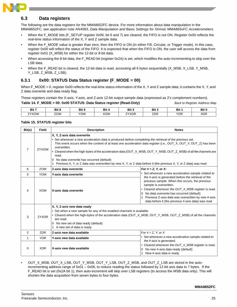
6.3.1 0x00: STATUS Data Status register (F_MODE = 00)
When F_MODE = 0, register 0x00 reflects the real-time status information of the X, Y and Z sample data; it contains the X, Y, and Z data overwrite and data ready flag.
These registers contain the X-axis, Y-axis, and Z-axis 12-bit output sample data (expressed as 2's complement numbers).
• OUT_X_MSB, OUT_X_LSB, OUT_Y_MSB, OUT_Y_LSB, OUT_Z_MSB, and OUT_Z_LSB are stored in the auto-incrementing address range of 0x01 – 0x06, to reduce reading the status followed by 12-bit axis data to 7 bytes. If the F_READ bit is set (0x2A bit 1), then auto-increment will skip over LSB registers (to access the MSB data only). This will shorten the data acquisition from seven bytes to four bytes.
Table 14. F_MODE = 00: 0x00 STATUS: Data Status register (Read-Only) Back to Register Address Map
Bit 7 Bit 6 Bit 5 Bit 4 Bit 3 Bit 2 Bit 1 Bit 0ZYXOW ZOW YOW XOW ZYXDR ZDR YDR XDR
Table 15. STATUS register bits
Bit(s) Field Description Notes
7 ZYXOW
X, Y, Z-axis data overwrite • Set whenever a new acceleration data is produced before completing the retrieval of the previous set.
This event occurs when the content of at least one acceleration data register (i.e., OUT_X, OUT_Y, OUT_Z) has been overwritten.
• Cleared when the high bytes of the acceleration data (OUT_X_MSB, OUT_Y_MSB, OUT_Z_MSB) of all the channels are read.
0 No data overwrite has occurred (default)1 Previous X, Y, or Z data was overwritten by new X, Y, or Z data before it (the previous X, Y, or Z data) was read
6 ZOW Z-axis data overwrite For # = Z, Y, or X:• Set whenever a new acceleration sample related to
the #-axis is generated before the retrieval of the previous sample. When this occurs, the previous sample is overwritten.
• Cleared whenever the OUT_#_MSB register is read.0 No data overwrite has occurred (default)1 Previous Z-axis data was overwritten by new #-axis
data before it (the previous #-axis data) was read
5 YOW Y-axis data overwrite
4 XOW X-axis data overwrite
3 ZYXDR
X, Y, Z-axis new data ready • Set when a new sample for any of the enabled channels is available. • Cleared when the high-bytes of the acceleration data (OUT_X_MSB, OUT_Y_MSB, OUT_Z_MSB) of all the channels
are read.0 No new set of data ready (default)1 A new set of data is ready
2 ZDR Z-axis new data available For # = Z, Y, or X• Set whenever a new acceleration sample related to
the #-axis is generated. • Cleared whenever the OUT_#_MSB register is read.0 No new #-axis data ready (default)1 New #-axis data is ready
1 YDR Y-axis new data available
0 XDR X-axis new data available
MMA8652FC
SensorsFreescale Semiconductor, Inc. 25

• The LSB registers can only be read immediately following the read access of the corresponding MSB register.
— A random read access to the LSB registers is not possible.
— Reading the MSB register and then the LSB register in sequence ensures that both bytes (LSB and MSB) belong to the same data sample, even if a new data sample arrives between reading the MSB and the LSB byte.
• If the FIFO is enabled (F_MODE > 00), then Register 0x01 points to the FIFO read pointer, while Registers 0x02, 0x03, 0x04, 0x05, 0x06 return a value of zero when read.
MMA8652FC
Sensors26 Freescale Semiconductor, Inc.
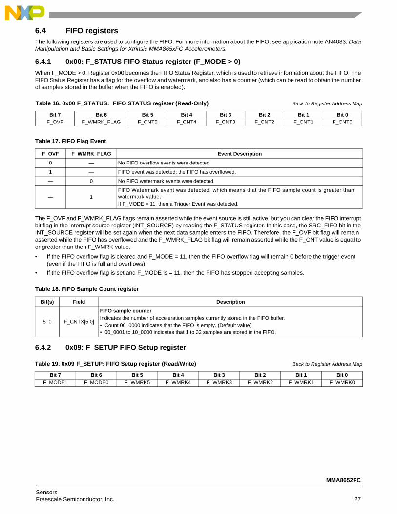
6.4 FIFO registersThe following registers are used to configure the FIFO. For more information about the FIFO, see application note AN4083, Data Manipulation and Basic Settings for Xtrinsic MMA865xFC Accelerometers.
6.4.1 0x00: F_STATUS FIFO Status register (F_MODE > 0)
When F_MODE > 0, Register 0x00 becomes the FIFO Status Register, which is used to retrieve information about the FIFO. The FIFO Status Register has a flag for the overflow and watermark, and also has a counter (which can be read to obtain the number of samples stored in the buffer when the FIFO is enabled).
The F_OVF and F_WMRK_FLAG flags remain asserted while the event source is still active, but you can clear the FIFO interrupt bit flag in the interrupt source register (INT_SOURCE) by reading the F_STATUS register. In this case, the SRC_FIFO bit in the INT_SOURCE register will be set again when the next data sample enters the FIFO. Therefore, the F_OVF bit flag will remain asserted while the FIFO has overflowed and the F_WMRK_FLAG bit flag will remain asserted while the F_CNT value is equal to or greater than then F_WMRK value.
• If the FIFO overflow flag is cleared and F_MODE = 11, then the FIFO overflow flag will remain 0 before the trigger event (even if the FIFO is full and overflows).
• If the FIFO overflow flag is set and F_MODE is = 11, then the FIFO has stopped accepting samples.
6.4.2 0x09: F_SETUP FIFO Setup register
Table 16. 0x00 F_STATUS: FIFO STATUS register (Read-Only) Back to Register Address Map
Bit 7 Bit 6 Bit 5 Bit 4 Bit 3 Bit 2 Bit 1 Bit 0F_OVF F_WMRK_FLAG F_CNT5 F_CNT4 F_CNT3 F_CNT2 F_CNT1 F_CNT0
Table 17. FIFO Flag Event
F_OVF F_WMRK_FLAG Event Description
0 — No FIFO overflow events were detected.
1 — FIFO event was detected; the FIFO has overflowed.
— 0 No FIFO watermark events were detected.
— 1FIFO Watermark event was detected, which means that the FIFO sample count is greater than watermark value.If F_MODE = 11, then a Trigger Event was detected.
Table 18. FIFO Sample Count register
Bit(s) Field Description
5–0 F_CNTX[5:0]
FIFO sample counter Indicates the number of acceleration samples currently stored in the FIFO buffer. • Count 00_0000 indicates that the FIFO is empty. (Default value)• 00_0001 to 10_0000 indicates that 1 to 32 samples are stored in the FIFO.
Table 19. 0x09 F_SETUP: FIFO Setup register (Read/Write) Back to Register Address Map
Bit 7 Bit 6 Bit 5 Bit 4 Bit 3 Bit 2 Bit 1 Bit 0F_MODE1 F_MODE0 F_WMRK5 F_WMRK4 F_WMRK3 F_WMRK2 F_WMRK1 F_WMRK0
MMA8652FC
SensorsFreescale Semiconductor, Inc. 27
The FIFO mode can be changed while in the Active mode. The Active mode must first be disabled (F_MODE = 00), before the mode can be switched between Fill mode, Circular mode, and Trigger mode.
A FIFO sample count exceeding the watermark event does not stop the FIFO from accepting new data. The FIFO update rate is dictated by the selected system ODR.
• In ACTIVE mode, the ODR is set by the DR bits (CTRL_REG1 register).
• When Auto-SLEEP is active, the ODR is set by the ASLP_RATE field (CTRL_REG1 register).
When a byte is read from the FIFO buffer, the oldest sample data in the FIFO buffer is returned (and also deleted from the front of the FIFO buffer), while the FIFO sample count is decremented by one. It is assumed that the host application will use the I2C multi-byte read transaction to empty the FIFO.
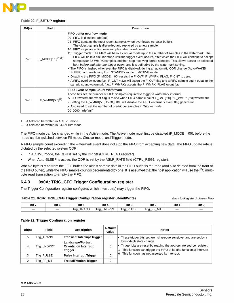
6.4.3 0x0A: TRIG_CFG Trigger Configuration register
The Trigger Configuration register configures which interrupt(s) may trigger the FIFO.
Table 20. F_SETUP register
Bit(s) Field Description
7–6 F_MODE[1:0](1)(2)
1. Bit field can be written in ACTIVE mode.2. Bit field can be written in STANDBY mode.
FIFO buffer overflow mode00 FIFO is disabled. (default)01 FIFO contains the most recent samples when overflowed (circular buffer).
The oldest sample is discarded and replaced by a new sample.10 FIFO stops accepting new samples when overflowed. 11 Trigger mode. The FIFO will be in a circular mode up to the number of samples in the watermark. The
FIFO will be in a circular mode until the trigger event occurs, after which the FIFO will continue to accept samples for 32-WMRK samples and then stop receiving further samples. This allows data to be collected both before and after the trigger event, and it is definable by the watermark setting.
• The FIFO is flushed whenever the FIFO is disabled, during an automatic ODR change (Auto-WAKE/SLEEP), or transitioning from STANDBY mode to ACTIVE mode.
• Disabling the FIFO (F_MODE = 00) resets the F_OVF, F_WMRK_FLAG, F_CNT to zero.• A FIFO overflow event (i.e., F_CNT = 32) will assert the F_OVF flag and a FIFO sample count equal to the
sample count watermark (i.e., F_WMRK) asserts the F_WMRK_FLAG event flag.
5–0 F_WMRK[5:0](2)
FIFO Event Sample Count Watermark These bits set the number of FIFO samples required to trigger a watermark interrupt. A FIFO watermark event flag is raised when FIFO sample count F_CNT[5:0] ≥ F_WMRK[5:0] watermark. • Setting the F_WMRK[5:0] to 00_0000 will disable the FIFO watermark event flag generation.• Also used to set the number of pre-trigger samples in Trigger mode.00_0000 (default)
Table 21. 0x0A: TRIG_CFG Trigger Configuration register (Read/Write) Back to Register Address Map
Bit 7 Bit 6 Bit 5 Bit 4 Bit 3 Bit 2 Bit 1 Bit 0— — Trig_TRANS Trig_LNDPRT Trig_PULSE Trig_FF_MT — —
Table 22. Trigger Configuration register
Bit(s) Field DescriptionDefault value
Notes
5 Trig_TRANS Transient Interrupt Trigger 0 • These trigger bits set are rising-edge sensitive, and are set by a low-to-high state change.
• Trigger bits are reset by reading the appropriate source register.1 This function can trigger the FIFO at its (the function’s) interrupt0 This function has not asserted its interrupt.
4 Trig_LNDPRTLandscape/Portrait Orientation Interrupt Trigger
0
3 Trig_PULSE Pulse Interrupt Trigger 0
2 Trig_FF_MT Freefall/Motion Trigger 0
MMA8652FC
Sensors28 Freescale Semiconductor, Inc.
6.5 System status and ID registers
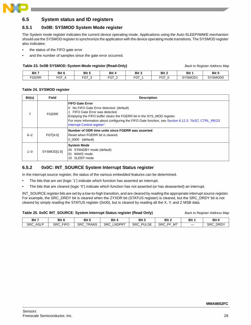
6.5.1 0x0B: SYSMOD System Mode register
The System mode register indicates the current device operating mode. Applications using the Auto-SLEEP/WAKE mechanism should use the SYSMOD register to synchronize the application with the device operating mode transitions. The SYSMOD register also indicates:
• the status of the FIFO gate error
• and the number of samples since the gate error occurred.
6.5.2 0x0C: INT_SOURCE System Interrupt Status register
In the interrupt source register, the status of the various embedded features can be determined.
• The bits that are set (logic ‘1’) indicate which function has asserted an interrupt.
• The bits that are cleared (logic ‘0’) indicate which function has not asserted (or has deasserted) an interrupt.
INT_SOURCE register bits are set by a low-to-high transition, and are cleared by reading the appropriate interrupt source register. For example, the SRC_DRDY bit is cleared when the ZYXDR bit (STATUS register) is cleared, but the SRC_DRDY bit is not cleared by simply reading the STATUS register (0x00), but is cleared by reading all the X, Y, and Z MSB data.
Table 23. 0x0B SYSMOD: System Mode register (Read-Only) Back to Register Address Map
Bit 7 Bit 6 Bit 5 Bit 4 Bit 3 Bit 2 Bit 1 Bit 0FGERR FGT_4 FGT_3 FGT_2 FGT_1 FGT_0 SYSMOD1 SYSMOD0
Table 24. SYSMOD register
Bit(s) Field Description
7 FGERR
FIFO Gate Error0 No FIFO Gate Error detected. (default)1 FIFO Gate Error was detected.Emptying the FIFO buffer clears the FGERR bit in the SYS_MOD register.For more information about configuring the FIFO Gate function, see Section 6.12.3, “0x2C: CTRL_REG3 Interrupt Control register”.
6–2 FGT[4:0]Number of ODR time units since FGERR was asserted. Reset when FGERR bit is cleared.0_0000 (default)
1–0 SYSMOD[1:0]
System Mode00 STANDBY mode (default)01 WAKE mode10 SLEEP mode
Table 25. 0x0C INT_SOURCE: System Interrupt Status register (Read Only) Back to Register Address Map
Bit 7 Bit 6 Bit 5 Bit 4 Bit 3 Bit 2 Bit 1 Bit 0SRC_ASLP SRC_FIFO SRC_TRANS SRC_LNDPRT SRC_PULSE SRC_FF_MT — SRC_DRDY
MMA8652FC
SensorsFreescale Semiconductor, Inc. 29
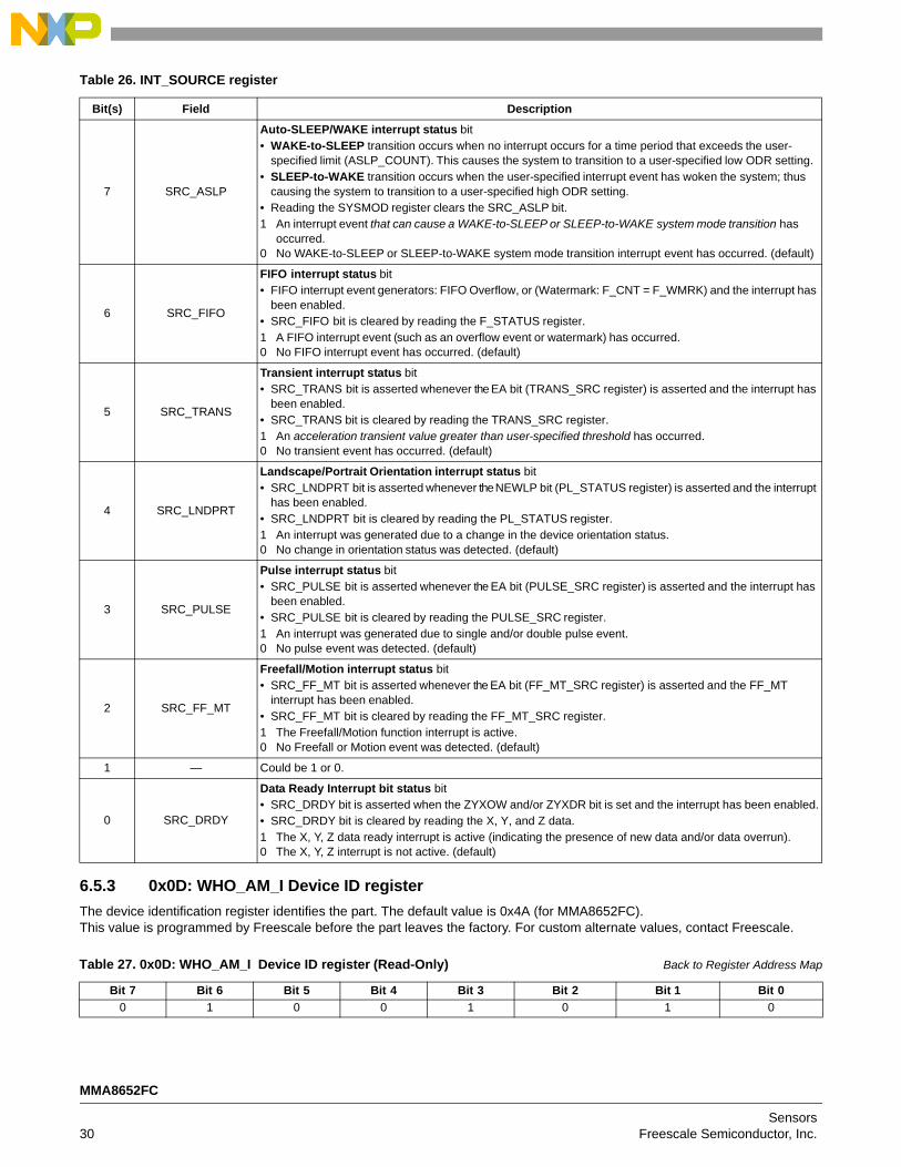
6.5.3 0x0D: WHO_AM_I Device ID register
The device identification register identifies the part. The default value is 0x4A (for MMA8652FC). This value is programmed by Freescale before the part leaves the factory. For custom alternate values, contact Freescale.
Table 26. INT_SOURCE register
Bit(s) Field Description
7 SRC_ASLP
Auto-SLEEP/WAKE interrupt status bit• WAKE-to-SLEEP transition occurs when no interrupt occurs for a time period that exceeds the user-
specified limit (ASLP_COUNT). This causes the system to transition to a user-specified low ODR setting.• SLEEP-to-WAKE transition occurs when the user-specified interrupt event has woken the system; thus
causing the system to transition to a user-specified high ODR setting.• Reading the SYSMOD register clears the SRC_ASLP bit.1 An interrupt event that can cause a WAKE-to-SLEEP or SLEEP-to-WAKE system mode transition has
occurred.0 No WAKE-to-SLEEP or SLEEP-to-WAKE system mode transition interrupt event has occurred. (default)
6 SRC_FIFO
FIFO interrupt status bit• FIFO interrupt event generators: FIFO Overflow, or (Watermark: F_CNT = F_WMRK) and the interrupt has
been enabled.• SRC_FIFO bit is cleared by reading the F_STATUS register.1 A FIFO interrupt event (such as an overflow event or watermark) has occurred. 0 No FIFO interrupt event has occurred. (default)
5 SRC_TRANS
Transient interrupt status bit• SRC_TRANS bit is asserted whenever the EA bit (TRANS_SRC register) is asserted and the interrupt has
been enabled. • SRC_TRANS bit is cleared by reading the TRANS_SRC register.1 An acceleration transient value greater than user-specified threshold has occurred. 0 No transient event has occurred. (default)
4 SRC_LNDPRT
Landscape/Portrait Orientation interrupt status bit• SRC_LNDPRT bit is asserted whenever the NEWLP bit (PL_STATUS register) is asserted and the interrupt
has been enabled.• SRC_LNDPRT bit is cleared by reading the PL_STATUS register.1 An interrupt was generated due to a change in the device orientation status. 0 No change in orientation status was detected. (default)
3 SRC_PULSE
Pulse interrupt status bit • SRC_PULSE bit is asserted whenever the EA bit (PULSE_SRC register) is asserted and the interrupt has
been enabled.• SRC_PULSE bit is cleared by reading the PULSE_SRC register.1 An interrupt was generated due to single and/or double pulse event. 0 No pulse event was detected. (default)
2 SRC_FF_MT
Freefall/Motion interrupt status bit• SRC_FF_MT bit is asserted whenever the EA bit (FF_MT_SRC register) is asserted and the FF_MT
interrupt has been enabled.• SRC_FF_MT bit is cleared by reading the FF_MT_SRC register.1 The Freefall/Motion function interrupt is active. 0 No Freefall or Motion event was detected. (default)
1 — Could be 1 or 0.
0 SRC_DRDY
Data Ready Interrupt bit status bit• SRC_DRDY bit is asserted when the ZYXOW and/or ZYXDR bit is set and the interrupt has been enabled.• SRC_DRDY bit is cleared by reading the X, Y, and Z data.1 The X, Y, Z data ready interrupt is active (indicating the presence of new data and/or data overrun). 0 The X, Y, Z interrupt is not active. (default)
Table 27. 0x0D: WHO_AM_I Device ID register (Read-Only) Back to Register Address Map
Bit 7 Bit 6 Bit 5 Bit 4 Bit 3 Bit 2 Bit 1 Bit 0
0 1 0 0 1 0 1 0
MMA8652FC
Sensors30 Freescale Semiconductor, Inc.
6.6 Data configuration registers
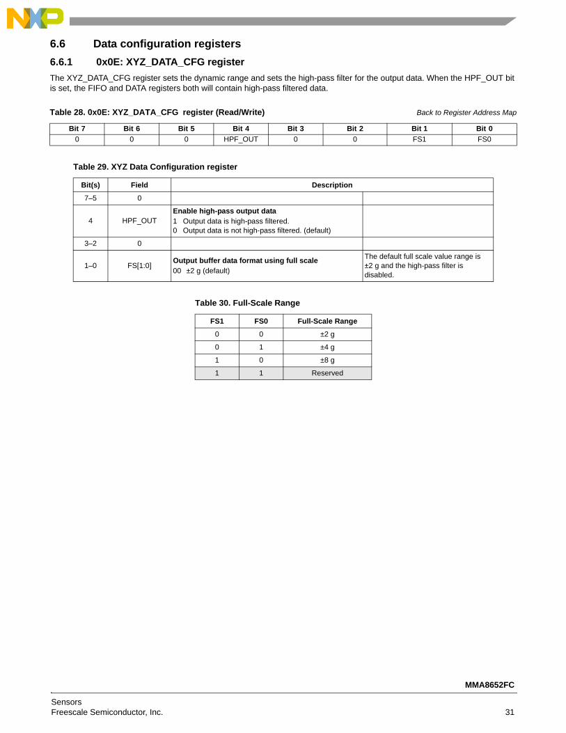
6.6.1 0x0E: XYZ_DATA_CFG register
The XYZ_DATA_CFG register sets the dynamic range and sets the high-pass filter for the output data. When the HPF_OUT bit is set, the FIFO and DATA registers both will contain high-pass filtered data.
Table 28. 0x0E: XYZ_DATA_CFG register (Read/Write) Back to Register Address Map
Bit 7 Bit 6 Bit 5 Bit 4 Bit 3 Bit 2 Bit 1 Bit 0
0 0 0 HPF_OUT 0 0 FS1 FS0
Table 29. XYZ Data Configuration register
Bit(s) Field Description
7–5 0
4 HPF_OUTEnable high-pass output data 1 Output data is high-pass filtered. 0 Output data is not high-pass filtered. (default)
3–2 0
1–0 FS[1:0]Output buffer data format using full scale 00 ±2 g (default)
The default full scale value range is ±2 g and the high-pass filter is disabled.
Table 30. Full-Scale Range
FS1 FS0 Full-Scale Range
0 0 ±2 g
0 1 ±4 g
1 0 ±8 g
1 1 Reserved
MMA8652FC
SensorsFreescale Semiconductor, Inc. 31
6.6.2 0x0F: HP_FILTER_CUTOFF High-Pass Filter register
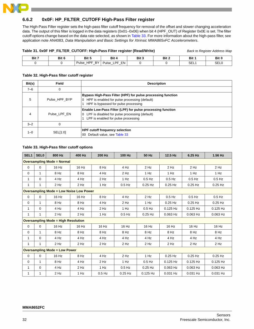
The High-Pass Filter register sets the high-pass filter cutoff frequency for removal of the offset and slower changing acceleration data. The output of this filter is logged in the data registers (0x01–0x06) when bit 4 (HPF_OUT) of Register 0x0E is set. The filter cutoff options change based on the data rate selected, as shown in Table 33. For more information about the high-pass filter, see application note AN4083, Data Manipulation and Basic Settings for Xtrinsic MMA865xFC Accelerometers.
Table 31. 0x0F HP_FILTER_CUTOFF: High-Pass Filter register (Read/Write) Back to Register Address Map
Bit 7 Bit 6 Bit 5 Bit 4 Bit 3 Bit 2 Bit 1 Bit 0
0 0 Pulse_HPF_BY Pulse_LPF_EN 0 0 SEL1 SEL0
Table 32. High-Pass filter cutoff register
Bit(s) Field Description
7–6 0
5 Pulse_HPF_BYPBypass High-Pass Filter (HPF) for pulse processing function0 HPF is enabled for pulse processing (default)1 HPF is bypassed for pulse processing
4 Pulse_LPF_ENEnable Low-Pass Filter (LPF) for pulse processing function0 LPF is disabled for pulse processing (default)1 LPF is enabled for pulse processing
3–2 0
1–0 SEL[1:0]HPF cutoff frequency selection00 Default value, see Table 33
Table 33. High-Pass filter cutoff options
SEL1 SEL0 800 Hz 400 Hz 200 Hz 100 Hz 50 Hz 12.5 Hz 6.25 Hz 1.56 Hz
Oversampling Mode = Normal
0 0 16 Hz 16 Hz 8 Hz 4 Hz 2 Hz 2 Hz 2 Hz 2 Hz
0 1 8 Hz 8 Hz 4 Hz 2 Hz 1 Hz 1 Hz 1 Hz 1 Hz
1 0 4 Hz 4 Hz 2 Hz 1 Hz 0.5 Hz 0.5 Hz 0.5 Hz 0.5 Hz
1 1 2 Hz 2 Hz 1 Hz 0.5 Hz 0.25 Hz 0.25 Hz 0.25 Hz 0.25 Hz
Oversampling Mode = Low Noise Low Power
0 0 16 Hz 16 Hz 8 Hz 4 Hz 2 Hz 0.5 Hz 0.5 Hz 0.5 Hz
0 1 8 Hz 8 Hz 4 Hz 2 Hz 1 Hz 0.25 Hz 0.25 Hz 0.25 Hz
1 0 4 Hz 4 Hz 2 Hz 1 Hz 0.5 Hz 0.125 Hz 0.125 Hz 0.125 Hz
1 1 2 Hz 2 Hz 1 Hz 0.5 Hz 0.25 Hz 0.063 Hz 0.063 Hz 0.063 Hz
Oversampling Mode = High Resolution
0 0 16 Hz 16 Hz 16 Hz 16 Hz 16 Hz 16 Hz 16 Hz 16 Hz
0 1 8 Hz 8 Hz 8 Hz 8 Hz 8 Hz 8 Hz 8 Hz 8 Hz
1 0 4 Hz 4 Hz 4 Hz 4 Hz 4 Hz 4 Hz 4 Hz 4 Hz
1 1 2 Hz 2 Hz 2 Hz 2 Hz 2 Hz 2 Hz 2 Hz 2 Hz
Oversampling Mode = Low Power
0 0 16 Hz 8 Hz 4 Hz 2 Hz 1 Hz 0.25 Hz 0.25 Hz 0.25 Hz
0 1 8 Hz 4 Hz 2 Hz 1 Hz 0.5 Hz 0.125 Hz 0.125 Hz 0.125 Hz
1 0 4 Hz 2 Hz 1 Hz 0.5 Hz 0.25 Hz 0.063 Hz 0.063 Hz 0.063 Hz
1 1 2 Hz 1 Hz 0.5 Hz 0.25 Hz 0.125 Hz 0.031 Hz 0.031 Hz 0.031 Hz
MMA8652FC
Sensors32 Freescale Semiconductor, Inc.
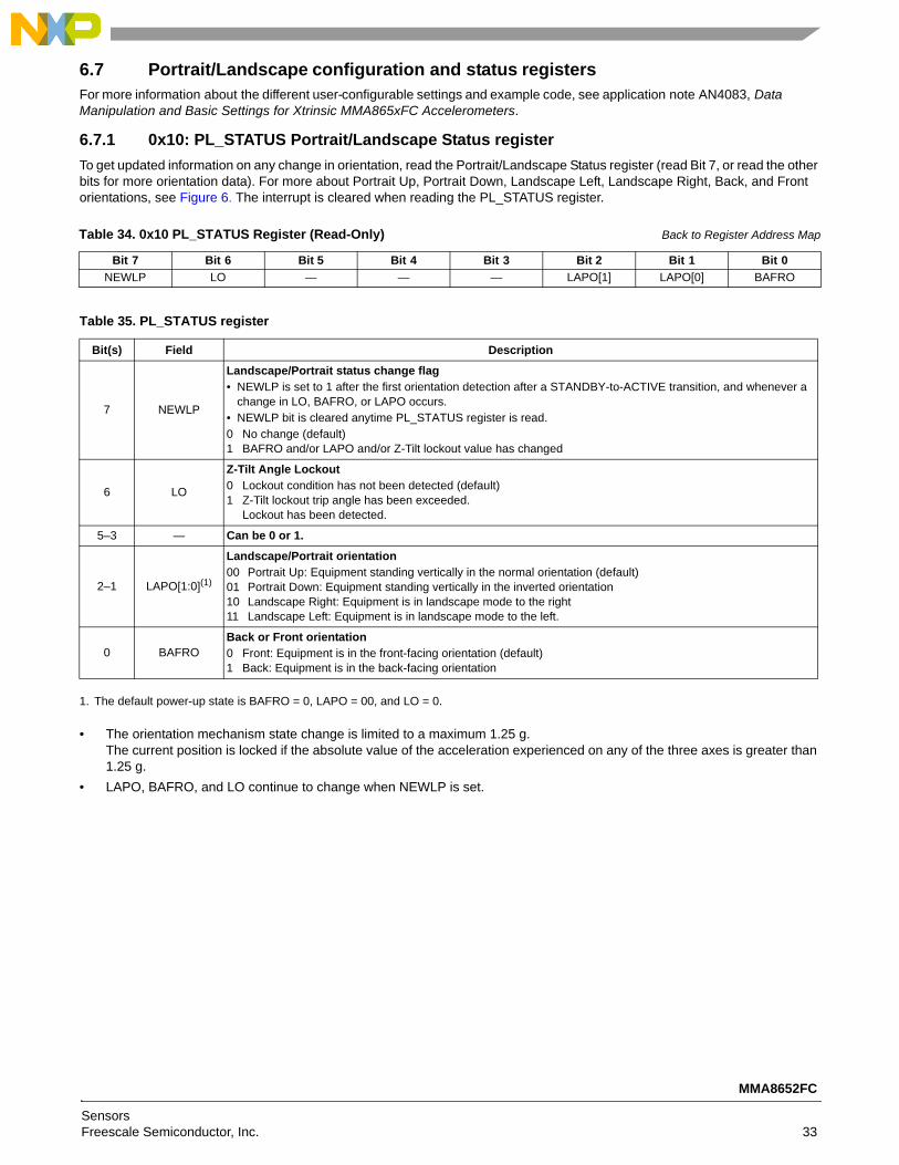
6.7 Portrait/Landscape configuration and status registersFor more information about the different user-configurable settings and example code, see application note AN4083, Data Manipulation and Basic Settings for Xtrinsic MMA865xFC Accelerometers.
6.7.1 0x10: PL_STATUS Portrait/Landscape Status register
To get updated information on any change in orientation, read the Portrait/Landscape Status register (read Bit 7, or read the other bits for more orientation data). For more about Portrait Up, Portrait Down, Landscape Left, Landscape Right, Back, and Front orientations, see Figure 6. The interrupt is cleared when reading the PL_STATUS register.
• The orientation mechanism state change is limited to a maximum 1.25 g. The current position is locked if the absolute value of the acceleration experienced on any of the three axes is greater than 1.25 g.
• LAPO, BAFRO, and LO continue to change when NEWLP is set.
Table 34. 0x10 PL_STATUS Register (Read-Only) Back to Register Address Map
Bit 7 Bit 6 Bit 5 Bit 4 Bit 3 Bit 2 Bit 1 Bit 0
NEWLP LO — — — LAPO[1] LAPO[0] BAFRO
Table 35. PL_STATUS register
Bit(s) Field Description
7 NEWLP
Landscape/Portrait status change flag• NEWLP is set to 1 after the first orientation detection after a STANDBY-to-ACTIVE transition, and whenever a
change in LO, BAFRO, or LAPO occurs. • NEWLP bit is cleared anytime PL_STATUS register is read. 0 No change (default)1 BAFRO and/or LAPO and/or Z-Tilt lockout value has changed
6 LO
Z-Tilt Angle Lockout0 Lockout condition has not been detected (default)1 Z-Tilt lockout trip angle has been exceeded.
Lockout has been detected.
5–3 — Can be 0 or 1.
2–1 LAPO[1:0](1)
1. The default power-up state is BAFRO = 0, LAPO = 00, and LO = 0.
Landscape/Portrait orientation00 Portrait Up: Equipment standing vertically in the normal orientation (default)01 Portrait Down: Equipment standing vertically in the inverted orientation 10 Landscape Right: Equipment is in landscape mode to the right11 Landscape Left: Equipment is in landscape mode to the left.
0 BAFROBack or Front orientation0 Front: Equipment is in the front-facing orientation (default)1 Back: Equipment is in the back-facing orientation
MMA8652FC
SensorsFreescale Semiconductor, Inc. 33
6.7.2 0x11 Portrait/Landscape Configuration register
The Portrait/Landscape Configuration register enables the portrait/landscape function and sets the behavior of the debounce counter.
6.7.3 0x12 Portrait/Landscape Debounce register
The Portrait/Landscape Debounce register sets the debounce count for the orientation state transition. The minimum debounce latency is determined by the data rate (which is set by the product of the selected system ODR and PL_COUNT registers). Any transition from WAKE to SLEEP (or SLEEP to Wake) resets the internal Landscape/Portrait debounce counter.
NOTEThe debounce counter weighting (time step) changes, based on the ODR and the Oversampling mode. Table 40 explains the time step value for all sample rates and all Oversampling modes.
Table 36. 0x11 PL_CFG register (Read/Write) Back to Register Address Map
Bit 7 Bit 6 Bit 5 Bit 4 Bit 3 Bit 2 Bit 1 Bit 0
DBCNTM PL_EN — — — — — —
Table 37. PL_CFG register
Bit(s) Field Description
7 DBCNTMDebounce counter mode selection0 Decrements debounce whenever the condition of interest is no longer valid.1 Clears the counter whenever the condition of interest is no longer valid. (default)
6 PL_ENPortrait/Landscape detection enable0 Portrait/Landscape Detection is disabled. (default)1 Portrait/Landscape Detection is enabled.
5–0 — Can be 0 or 1.
Table 38. 0x12 PL_COUNT register (Read/Write) Back to Register Address Map
Bit 7 Bit 6 Bit 5 Bit 4 Bit 3 Bit 2 Bit 1 Bit 0
DBNCE[7] DBNCE[6] DBNCE[5] DBNCE[4] DBNCE[3] DBNCE[2] DBNCE[1] DBNCE[0]
Table 39. PL_COUNT register
Bit(s) Field Description
7–0 DBCNE[7:0]Debounce Count value0000_0000 (default)
Table 40. PL_COUNT relationship with the ODR
ODR (Hz)
Max Time Range (s) Time Step (ms)
Normal LPLN HighRes LP Normal LPLN HighRes LP
800 0.319 0.319 0.319 0.319 1.25 1.25 1.25 1.25
400 0.638 0.638 0.638 0.638 2.5 2.5 2.5 2.5
200 1.28 1.28 0.638 1.28 5 5 2.5 5
100 2.55 2.55 0.638 2.55 10 10 2.5 10
50 5.1 5.1 0.638 5.1 20 20 2.5 20
12.5 5.1 20.4 0.638 20.4 20 80 2.5 80
6.25 5.1 20.4 0.638 40.8 20 80 2.5 160
1.56 5.1 20.4 0.638 40.8 20 80 2.5 160
MMA8652FC
Sensors34 Freescale Semiconductor, Inc.
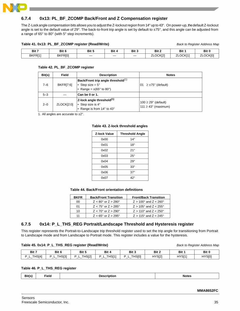
6.7.4 0x13: PL_BF_ZCOMP Back/Front and Z Compensation register
The Z-Lock angle compensation bits allows you to adjust the Z-lockout region from 14° up to 43°. On power-up, the default Z-lockout angle is set to the default value of 29°. The back-to-front trip angle is set by default to ±75°, and this angle can be adjusted from a range of 65° to 80° (with 5° step increments).
6.7.5 0x14: P_L_THS_REG Portrait/Landscape Threshold and Hysteresis register
This register represents the Portrait-to-Landscape trip threshold register used to set the trip angle for transitioning from Portrait to Landscape mode and from Landscape to Portrait mode. This register includes a value for the hysteresis.
Table 41. 0x13: PL_BF_ZCOMP register (Read/Write) Back to Register Address Map
Bit 7 Bit 6 Bit 5 Bit 4 Bit 3 Bit 2 Bit 1 Bit 0
BKFR[1] BKFR[0] — — — ZLOCK[2] ZLOCK[1] ZLOCK[0]
Table 42. PL_BF_ZCOMP register
Bit(s) Field Description Notes
7–6 BKFR[7:6]Back/Front trip angle threshold(1) • Step size = 5°• Range = ±(65° to 80°)
1. All angles are accurate to ±2°.
01 ≥ ±75° (default)
5–3 — Can be 0 or 1.
2–0 ZLOCK[2:0]Z-lock angle threshold(1)
• Step size is 4°• Range is from 14° to 43°
100 ≥ 29° (default) 111 ≥ 43° (maximum)
Table 43. Z-lock threshold angles
Z-lock Value Threshold Angle
0x00 14°
0x01 18°
0x02 21°
0x03 25°
0x04 29°
0x05 33°
0x06 37°
0x07 42°
Table 44. Back/Front orientation definitions
BKFR Back/Front Transition Front/Back Transition00 Z < 80° or Z > 280° Z > 100° and Z < 260°
01 Z < 75° or Z > 285° Z > 105° and Z < 255°
10 Z < 70° or Z > 290° Z > 110° and Z < 250°
11 Z < 65° or Z > 295° Z > 115° and Z < 245°
Table 45. 0x14: P_L_THS_REG register (Read/Write) Back to Register Address Map
Bit 7 Bit 6 Bit 5 Bit 4 Bit 3 Bit 2 Bit 1 Bit 0
P_L_THS[4] P_L_THS[3] P_L_THS[2] P_L_THS[1] P_L_THS[0] HYS[2] HYS[1] HYS[0]
Table 46. P_L_THS_REG register
Bit(s) Field Description Notes
MMA8652FC
SensorsFreescale Semiconductor, Inc. 35
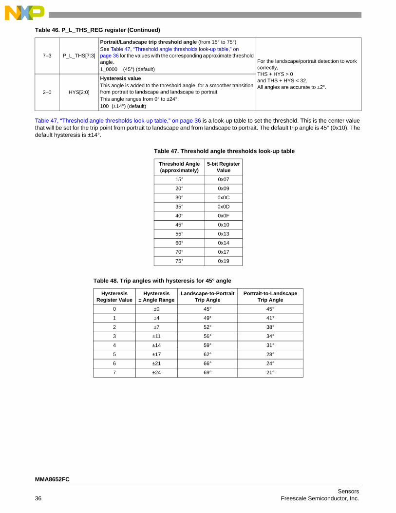
Table 47, “Threshold angle thresholds look-up table,” on page 36 is a look-up table to set the threshold. This is the center value that will be set for the trip point from portrait to landscape and from landscape to portrait. The default trip angle is 45° (0x10). The default hysteresis is ±14°.
7–3 P_L_THS[7:3]
Portrait/Landscape trip threshold angle (from 15° to 75°) See Table 47, “Threshold angle thresholds look-up table,” on page 36 for the values with the corresponding approximate threshold angle. 1_0000 (45°) (default)
For the landscape/portrait detection to work correctly, THS + HYS > 0 and THS + HYS < 32. All angles are accurate to ±2°.
2–0 HYS[2:0]
Hysteresis valueThis angle is added to the threshold angle, for a smoother transition from portrait to landscape and landscape to portrait. This angle ranges from 0° to ±24°. 100 (±14°) (default)
Table 47. Threshold angle thresholds look-up table
Threshold Angle(approximately)
5-bit Register Value
15° 0x07
20° 0x09
30° 0x0C
35° 0x0D
40° 0x0F
45° 0x10
55° 0x13
60° 0x14
70° 0x17
75° 0x19
Table 48. Trip angles with hysteresis for 45° angle
HysteresisRegister Value
Hysteresis± Angle Range
Landscape-to-PortraitTrip Angle
Portrait-to-LandscapeTrip Angle
0 ±0 45° 45°
1 ±4 49° 41°
2 ±7 52° 38°
3 ±11 56° 34°
4 ±14 59° 31°
5 ±17 62° 28°
6 ±21 66° 24°
7 ±24 69° 21°
Table 46. P_L_THS_REG register (Continued)
MMA8652FC
Sensors36 Freescale Semiconductor, Inc.

6.8 Freefall/Motion configuration and status registersThe freefall/motion function can be configured in either Freefall or Motion Detection mode via the OAE configuration bit (0x15: FF_MTG_CFG, bit 6). The freefall/motion detection block can be disabled by setting all three bits (ZEFE, YEFE, XEFE) to zero.
Depending on the register bits ELE (0x15: FF_MTG_CFG, bit 7) and OAE (0x15: FF_MTG_CFG, bit 6), each of the freefall and motion detection block can operate in four different modes.
6.8.1 Motion and freefall modes
6.8.1.1 Mode 1: Freefall detection with ELE = 0, OAE = 0
In this mode, the EA bit (0x16: FF_MTG_CFG, bit 7) indicates a freefall event after the debounce counter is complete. The ZEFE, YEFE, and XEFE control bits determine which axes are considered for the freefall detection. Once the EA bit is set, and DBCNTM = 0, the EA bit can get cleared only after the delay specified by FF_MT_COUNT. This is because the counter is in decrement mode. If DBCNTM = 1, then the EA bit is cleared as soon as the freefall condition disappears, and will not be set again before the delay specified by FF_MT_COUNT has passed. Reading the FF_MT_SRC register does not clear the EA bit.
The event flags (0x16) ZHE, ZHP, YHE, YHP, XHE, and XHP reflect the motion detection status (i.e., a high g event) without any debouncing, provided that the corresponding bits ZEFE, YEFE, and/or XEFE are set.
6.8.1.2 Mode 2: Freefall detection with ELE = 1, OAE = 0
In this mode, the EA event bit indicates a freefall event after the debounce counter. Once the debounce counter reaches the time value for the set threshold, the EA bit is set, and the EA bit remains set until the FF_MT_SRC register is read. When the FF_MT_SRC register is read, the EA bit and the debounce counter are cleared, and a new event can only be generated after the delay specified by FF_MT_CNT. The ZEFE, YEFE, and XEFE control bits determine which axes are considered for the freefall detection. While EA = 0, the event flags ZHE, ZHP, YHE, YHP, XHE, and XHP reflect the motion detection status (i.e., a high g event) without any debouncing, provided that the corresponding bits ZEFE, YEFE, and/or XEFE are set.
The event flags ZHE, ZHP, YHE, YHP, XHE, and XHP are latched when the EA event bit is set. The event flags ZHE, ZHP, YHE, YHP, XHE, and XHP will start changing only after the FF_MT_SRC register has been read.
6.8.1.3 Mode 3: Motion detection with ELE = 0, OAE = 1
In this mode, the EA bit indicates a motion event after the debounce counter time is reached. The ZEFE, YEFE, and XEFE control bits determine which axes are taken into consideration for motion detection. Once the EA bit is set and if DBCNTM = 0, the EA bit can get cleared only after the delay specified by FF_MT_COUNT. If DBCNTM = 1, then the EA bit is cleared as soon as the motion high g condition disappears.
The event flags ZHE, ZHP, YHE, YHP, XHE, and XHP reflect the motion detection status (i.e., a high g event) without any debouncing, provided that the corresponding bits ZEFE, YEFE, and/or XEFE are set. Reading the FF_MT_SRC does not clear any flags, nor is the debounce counter reset.
6.8.1.4 Mode 4: Motion detection with ELE = 1, OAE = 1
In this mode, the EA bit indicates a motion event after debouncing. The ZEFE, YEFE, and XEFE control bits determine which axes are taken into consideration for motion detection. Once the debounce counter reaches the threshold, the EA bit is set, and the EA bit remains set until the FF_MT_SRC register is read. When the FF_MT_SRC register is read, all register bits are cleared and the debounce counter are cleared and a new event can only be generated after the delay specified by FF_MT_CNT.
While the bit EA is zero, the event flags ZHE, ZHP, YHE, YHP, XHE, and XHP reflect the motion detection status (i.e., a high g event) without any debouncing, provided that the corresponding bits ZEFE, YEFE, and/or XEFE are set. When the EA bit is set, these bits (ZHE, ZHP, YHE, YHP, XHE, XHP) keep their current value until the FF_MT_SRC register is read.
MMA8652FC
SensorsFreescale Semiconductor, Inc. 37
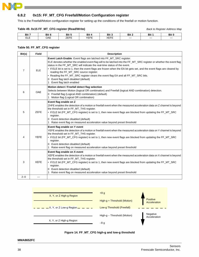
6.8.2 0x15: FF_MT_CFG Freefall/Motion Configuration register
This is the Freefall/Motion configuration register for setting up the conditions of the freefall or motion function.
Figure 14. FF_MT_CFG high-g and low-g threshold
Table 49. 0x15 FF_MT_CFG register (Read/Write) Back to Register Address Map
Bit 7 Bit 6 Bit 5 Bit 4 Bit 3 Bit 2 Bit 1 Bit 0ELE OAE ZEFE YEFE XEFE — — —
Table 50. FF_MT_CFG register
Bit(s) Field Description
7 ELE
Event Latch Enable: Event flags are latched into FF_MT_SRC register. ELE denotes whether the enabled event flag will to be latched into the FF_MT_SRC register or whether the event flag status in the FF_MT_SRC will indicate the real-time status of the event. • If ELE bit is set to 1, then the event flags are frozen when the EA bit gets set, and the event flags are cleared by
reading the FF_MT_SRC source register. • Reading the FF_MT_SRC register clears the event flag EA and all FF_MT_SRC bits. 0 Event flag latch disabled (default)1 Event flag latch enabled
6 OAE
Motion detect / Freefall detect flag selectionSelects between Motion (logical OR combination) and Freefall (logical AND combination) detection. 0 Freefall flag (Logical AND combination) (default)1 Motion flag (Logical OR combination)
5 ZEFE
Event flag enable on ZZHFE enables the detection of a motion or freefall event when the measured acceleration data on Z channel is beyond the threshold set in FF_MT_THS register. • If ELE bit (FF_MT_CFG register) is set to 1, then new event flags are blocked from updating the FF_MT_SRC
register.0 Event detection disabled (default)1 Raise event flag on measured acceleration value beyond preset threshold
4 YEFE
Event flag enable on Y eventYEFE enables the detection of a motion or freefall event when the measured acceleration data on Y channel is beyond the threshold set in FF_MT_THS register.• If ELE bit (FF_MT_CFG register) is set to 1, then new event flags are blocked from updating the FF_MT_SRC
register. 0 Event detection disabled (default)1 Raise event flag on measured acceleration value beyond preset threshold
3 XEFE
Event flag enable on X eventXEFE enables the detection of a motion or freefall event when the measured acceleration data on X channel is beyond the threshold set in FF_MT_THS register. • If ELE bit (FF_MT_CFG register) is set to 1, then new event flags are blocked from updating the FF_MT_SRC
register. 0 Event detection disabled (default)1 Raise event flag on measured acceleration value beyond preset threshold
2–0 —
+8 g
High-g + Threshold (Motion)
Low-g Threshold (Freefall)
High-g – Threshold (Motion)
–8 g
X, Y, or Z High-g Region
X, Y, or Z High-g Region
X, Y, or Z Low-g Region
Negative
Positive
Acceleration
Acceleration
MMA8652FC
Sensors38 Freescale Semiconductor, Inc.
6.8.3 0x16: FF_MT_SRC Freefall/Motion Source register
The Freefall/Motion Source register keeps track of the acceleration event that is triggering (or has triggered, if ELE bit in FF_MT_CFG register is set to 1) the event flag. In particular, EA is set to 1 when the logical combination of acceleration events flags specified in FF_MT_CFG register is true. This EA bit is used in combination with the values in INT_EN_FF_MT and INT_CFG_FF_MT register bits to generate the freefall/motion interrupts.
• An X,Y, or Z motion is true when the acceleration value of the X or Y or Z channel is higher than the preset threshold value defined in the FF_MT_THS register.
• An X, Y, and Z low event is true when the acceleration value of the X and Y and Z channel is lower than or equal to the preset threshold value defined in the FF_MT_THS register.
Table 51. 0x16: FF_MT_SRC Freefall/Motion Source register (Read-Only) Back to Register Address Map
Bit 7 Bit 6 Bit 5 Bit 4 Bit 3 Bit 2 Bit 1 Bit 0EA — ZHE ZHP YHE YHP XHE XHP
Table 52. Freefall/Motion Source register
Bit(s) Field Description
7 EA
Event Active flag0 No event flag has been asserted (default)1 One or more event flags has been asserted.
See the description of the OAE bit to determine the effect of the 3-axis event flags on the EA bit.
6 —
5 ZHE
Z-Motion flag ZHE bit always reads zero if the ZEFE control bit is set to zero.0 No Z motion event detected (default)1 Z motion has been detected
4 ZHP
Z-Motion Polarity Flag ZHP bit always reads zero if the ZEFE control bit is set to zero.0 Z event was positive g (default)1 Z event was negative g
3 YHE
Y-Motion Flag YHE bit always reads zero if the YEFE control bit is set to zero.0 No Y motion event detected (default)1 Y motion has been detected
2 YHP
Y-Motion Polarity Flag YHP bit always reads zero if the YEFE control bit is set to zero.0 Y event detected was positive g (default)1 Y event was negative g
1 XHE
X-Motion Flag XHE bit always reads zero if the XEFE control bit is set to zero.0 No X motion event detected (default)1 X motion has been detected
0 XHP
X-Motion Polarity Flag XHP bit always reads zero if the XEFE control bit is set to zero.0 X event was positive g (default)1 X event was negative g
MMA8652FC
SensorsFreescale Semiconductor, Inc. 39
6.8.4 0x17: FF_MT_THS Freefall and Motion Threshold register
FF_MT_THS is the threshold register used to detect freefall motion events.
• The unsigned 7-bit FF_MT_THS threshold register holds the threshold for the freefall detection where the magnitude of the X and Y and Z acceleration values is lower or equal than the threshold value.
• Conversely, the FF_MT_THS also holds the threshold for the motion detection where the magnitude of the X or Y or Z acceleration value is higher than the threshold value.
The threshold resolution is 0.063 g/LSB and the threshold register has a range of 0 to 127 counts. The maximum range is to ±8 g. Note that even when the full scale value is set to ±2 g or ±4 g, the motion still detects up to ±8 g.
The DBCNTM bit configures the way in which the debounce counter is reset when the inertial event of interest is momentarily not true.
• When the DBCNTM bit is 1, the debounce counter is cleared to 0 whenever the inertial event of interest is no longer true as shown in Figure 15, (b).
• While the DBCNTM bit is set to 0, the debounce counter is decremented by 1 whenever the inertial event of interest is no longer true (Figure 15, (c)) until the debounce counter reaches 0 or until the inertial event of interest becomes active.
Decrementing the debounce counter acts as a median enabling the system to filter out irregular spurious events (which might impede the detection of inertial events).
6.8.5 0x18 FF_MT_COUNT Debounce register
The Debounce register sets the number of debounce sample counts for the event trigger.
The Debounce register sets the minimum number of debounce sample counts that continuously match the detection condition selected by you for the freefall/motion event.
When the internal debounce counter reaches the FF_MT_COUNT value, a freefall/motion event flag is set. The debounce counter will never increase beyond the FF_MT_COUNT value. The time step used for the debounce sample count depends on the ODR chosen and the Oversampling mode, as shown in Table 57.
Table 53. 0x17 FF_MT_THS register (Read/Write) Back to Register Address Map
Bit 7 Bit 6 Bit 5 Bit 4 Bit 3 Bit 2 Bit 1 Bit 0DBCNTM THS6 THS5 THS4 THS3 THS2 THS1 THS0
Table 54. FF_MT_THS register
Bit(s) Field Description
7 DBCNTMDebounce counter mode selection0 Increments or decrements debounce (default)1 Increments or clears counter.
6–0 THS[6:0]Freefall /Motion Threshold000_0000 (default)
Table 55. 0x18 FF_MT_COUNT register (Read/Write) Back to Register Address Map
Bit 7 Bit 6 Bit 5 Bit 4 Bit 3 Bit 2 Bit 1 Bit 0D7 D6 D5 D4 D3 D2 D1 D0
Table 56. FF_MT_COUNT register
Bit(s) Field Description
7–0 D[7:0]Count value0000_0000 (default)
MMA8652FC
Sensors40 Freescale Semiconductor, Inc.
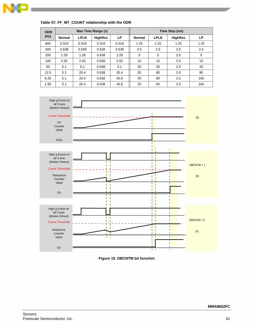
Figure 15. DBCNTM bit function
Table 57. FF_MT_COUNT relationship with the ODR
ODR (Hz)
Max Time Range (s) Time Step (ms)
Normal LPLN HighRes LP Normal LPLN HighRes LP
800 0.319 0.319 0.319 0.319 1.25 1.25 1.25 1.25
400 0.638 0.638 0.638 0.638 2.5 2.5 2.5 2.5
200 1.28 1.28 0.638 1.28 5 5 2.5 5
100 2.55 2.55 0.638 2.55 10 10 2.5 10
50 5.1 5.1 0.638 5.1 20 20 2.5 20
12.5 5.1 20.4 0.638 20.4 20 80 2.5 80
6.25 5.1 20.4 0.638 40.8 20 80 2.5 160
1.56 5.1 20.4 0.638 40.8 20 80 2.5 160
High g Event on
Count Threshold
FF
FFEA
all 3-axis(Motion Detect)
CounterValue
High g Event on
Count Threshold
Debounce
(a)
all 3-axis(Motion Detect)
CounterValue
High g Event on
Count Threshold
Debounce
EA
all 3-axis(Motion Detect)
CounterValue
DBCNTM = 1
(b)
EA
DBCNTM = 0
(c)
MMA8652FC
SensorsFreescale Semiconductor, Inc. 41
6.9 Transient configuration and status registersFor more information about the uses of the transient function, see application note AN4083, Data Manipulation and Basic Settings for Xtrinsic MMA865xFC Accelerometers. This Transient (HPF) acceleration detection function is similar to the motion detection function, except that high-pass filtered data is compared.
There is an option to disable the high-pass filter through the function. In this case, the behavior is the same as the motion detection. This allows for the device to have two motion detection functions.
6.9.1 0x1D: Transient_CFG register
The transient detection mechanism can be configured to raise an interrupt when the magnitude of the high-pass filtered acceleration threshold is exceeded. The TRANSIENT_CFG register is used to enable the transient interrupt generation mechanism for the three axes (X, Y, Z) of acceleration. There is also an option to bypass the high-pass filter. When the high-pass filter is bypassed, the function behaves similar to the motion detection.
Table 58. 0x1D TRANSIENT_CFG register (Read/Write) Back to Register Address Map
Bit 7 Bit 6 Bit 5 Bit 4 Bit 3 Bit 2 Bit 1 Bit 0— — — ELE ZTEFE YTEFE XTEFE HPF_BYP
Table 59. TRANSIENT_CFG register
Bit(s) Field Description Notes
7–5 — Could be 0 or 1.
4 ELE
Transient event flags are latched into the TRANSIENT_SRC register. Reading of the TRANSIENT_SRC register clears the event flag. 0 Event flag latch disabled (default)1 Event flag latch enabled
3 ZTEFEEvent flag enable for Z-transient acceleration greater than a transient threshold event.
0 Event detection disabled (default)1 Raise event flag on measured acceleration delta
value that is greater than a transient threshold.
2 YTEFEEvent flag enable for Y-transient acceleration greater than a transient threshold event.
1 XTEFEEvent flag enable for X-transient acceleration greater than a transient threshold event.
0 HPF_BYP
Bypass high-pass filter0 Data to transient acceleration detection block is through HPF
(default)1 Data to transient acceleration detection block is NOT through
HPF (similar to motion detection function)
MMA8652FC
Sensors42 Freescale Semiconductor, Inc.
6.9.2 0x1E TRANSIENT_SRC register
The transient source register provides the status of the enabled axes and the polarity (directional) information. When the TRANSIENT_SRC register is read, it clears the interrupt for the transient detection.
When new events arrive while EA = 1, additional *TRANSE bits may get set, and the corresponding *_Trans_Pol flag become updated. However no *TRANSE bit may get cleared before the TRANSIENT_SRC register is read.
• When the EA bit gets set while ELE = 1, all other status bits get frozen at their current state.
• By reading the TRANSIENT_SRC register, all bits get cleared.
Table 60. 0x1E TRANSIENT_SRC register (Read-Only) Back to Register Address Map
Bit 7 Bit 6 Bit 5 Bit 4 Bit 3 Bit 2 Bit 1 Bit 0— EA ZTRANSE Z_Trans_Pol YTRANSE Y_Trans_Pol XTRANSE X_Trans_Pol
Table 61. TRANSIENT_SRC register
Bit(s) Field Description
7 — Could be 0 or 1.
6 EAEvent Active Flag 0 No event flag has been asserted (default)1 One or more event flags has been asserted.
5 ZTRANSEZ-transient event 0 No interrupt (default)1 Z-transient acceleration greater than the value of TRANSIENT_THS event has occurred
4 Z_Trans_PolPolarity of Z-Transient Event that triggered the interrupt 0 Z-event was positive g (default)1 Z-event was negative g
3 YTRANSEY-transient event 0 No interrupt (default)1 Y-transient acceleration greater than the value of TRANSIENT_THS event has occurred
2 Y_Trans_PolPolarity of Y-Transient Event that triggered the interrupt 0 Y-event was Positive g (default)1 Y-event was Negative g
1 XTRANSEX-transient event 0 No interrupt (default)1 X-transient acceleration greater than the value of TRANSIENT_THS event has occurred
0 X_Trans_PolPolarity of X-Transient Event that triggered the interrupt 0 X-event was Positive g (default)1 X-event was Negative g
MMA8652FC
SensorsFreescale Semiconductor, Inc. 43
6.9.3 0x1F TRANSIENT_THS register
The Transient Threshold register sets the threshold limit for the detection of the transient acceleration. The value in the TRANSIENT_THS register corresponds to a g value, which is compared against the values of high-pass filtered data. If the high-pass filtered acceleration value exceeds the threshold limit, an event flag is raised and the interrupt is generated (if enabled).
6.9.4 0x20 TRANSIENT_COUNT register
The TRANSIENT_COUNT sets the minimum number of debounce counts continuously matching the condition where the unsigned value of high-pass filtered data is greater than the user-specified value of TRANSIENT_THS.
The time step for the transient detection debounce counter is set by the value of the system ODR and the Oversampling mode.
Table 62. 0x1F TRANSIENT_THS register (Read/Write) Back to Register Address Map
Bit 7 Bit 6 Bit 5 Bit 4 Bit 3 Bit 2 Bit 1 Bit 0DBCNTM THS6 THS5 THS4 THS3 THS2 THS1 THS0
Table 63. TRANSIENT_THS register
Bit(s) Field Description Notes
7 DBCNTMDebounce counter mode selection0 Increments or decrements debounce (default)1 Increments or clears counter
6–0 THS[6:0]
Transient ThresholdA 7-bit unsigned number, with 0.063 g/LSB.The maximum threshold is ±8 g. 000_0000 (default)
Even if the part is set to full scale at ±2 g (or ±4 g), this function will still operate up to ±8 g.
Table 64. 0x20 TRANSIENT_COUNT register (Read/Write) Back to Register Address Map
Bit 7 Bit 6 Bit 5 Bit 4 Bit 3 Bit 2 Bit 1 Bit 0D7 D6 D5 D4 D3 D2 D1 D0
Table 65. TRANSIENT_COUNT register
Bit(s) Field Description
7–0 D[7:0]Count value0000_0000 (default)
Table 66. TRANSIENT_COUNT relationship with the ODR
ODR (Hz) Max Time Range (s) Time Step (ms)
Normal LPLN HighRes LP Normal LPLN HighRes LP
800 0.319 0.319 0.319 0.319 1.25 1.25 1.25 1.25
400 0.638 0.638 0.638 0.638 2.5 2.5 2.5 2.5
200 1.28 1.28 0.638 1.28 5 5 2.5 5
100 2.55 2.55 0.638 2.55 10 10 2.5 10
50 5.1 5.1 0.638 5.1 20 20 2.5 20
12.5 5.1 20.4 0.638 20.4 20 80 2.5 80
6.25 5.1 20.4 0.638 40.8 20 80 2.5 160
1.56 5.1 20.4 0.638 40.8 20 80 2.5 160
MMA8652FC
Sensors44 Freescale Semiconductor, Inc.
6.10 Pulse configuration and status registersFor more information about of how to configure the tap detection and sample code, see application note AN4083, Data Manipulation and Basic Settings for Xtrinsic MMA865xFC Accelerometers. The tap detection registers are referred to as “Pulse”.
6.10.1 0x21: PULSE_CFG Pulse Configuration register
The PULSE_CFG register configures the event flag for tap detection, enabling/disabling the detection of a single and double pulse on each of the axes.
Table 67. 0x21 PULSE_CFG register (Read/Write) Back to Register Address Map
Bit 7 Bit 6 Bit 5 Bit 4 Bit 3 Bit 2 Bit 1 Bit 0
DPA ELE ZDPEFE ZSPEFE YDPEFE YSPEFE XDPEFE XSPEFE
Table 68. PULSE_CFG register
Bit(s) Field Description Notes
7 DPA
Double Pulse Abort0 Double Pulse detection is not aborted if the start of a pulse is detected during
the time period specified by the PULSE_LTCY register. (default)1 Setting the DPA bit momentarily suspends the double tap detection if the
start of a pulse is detected during the time period specified by the PULSE_LTCY register, and the pulse ends before the end of the time period specified by the PULSE_LTCY register.
6 ELEPulse event flags are latched into the PULSE_SRC register. Reading of the PULSE_SRC register clears the event flag.
0 Event detection is disabled (default)1 Event detection is enabled
5 ZDPEFE Event flag enable for a double pulse event on Z-axis
4 ZSPEFE Event flag enable for a single pulse event on Z-axis
3 YDPEFE Event flag enable for a double pulse event on Y-axis
2 YSPEFE Event flag enable for a single pulse event on Y-axis
1 XDPEFE Event flag enable for a double pulse event on X-axis
0 XSPEFE Event flag enable for a single pulse event on X-axis
MMA8652FC
SensorsFreescale Semiconductor, Inc. 45
6.10.2 0x22: PULSE_SRC Pulse Source register
The PULSE_SRC register indicates a double or single pulse event has occurred (and also which direction). The corresponding axis and event must be enabled in register 0x21 for the event flag to be asserted in the source register.
• When the EA bit gets set while ELE = 1, all status bits (AxZ, AxY, AxZ, DPE, and PolX, PolY, PolZ) are frozen.
• Reading the PULSE_SRC register clears all bits.
• Reading the source register will clear the interrupt.
Table 69. 0x22 PULSE_SRC register (Read-Only) Back to Register Address Map
Bit 7 Bit 6 Bit 5 Bit 4 Bit 3 Bit 2 Bit 1 Bit 0 EA AxZ AxY AxX DPE PolZ PolY PolX
Table 70. PULSE_SRC register
Bit Field Description
7 EAEvent Active Flag0 No interrupt has been generated (default)1 One or more interrupt events have been generated
6 AxZZ-axis event0 No interrupt (default)1 Z-axis event has occurred
5 AxYY-axis event0 No interrupt (default)1 Y-axis event has occurred)
4 AxXX-axis event0 No interrupt (default)1 X-axis event has occurred
3 DPEDouble pulse on first event0 Single pulse event triggered interrupt (default)1 Double pulse event triggered interrupt
2 PolZPulse polarity of Z-axis event0 Pulse event that triggered interrupt was positive (default)1 Pulse event that triggered interrupt was negative)
1 PolYPulse polarity of Y-axis event0 Pulse event that triggered interrupt was positive (default)1 Pulse event that triggered interrupt was negative
0 PolXPulse polarity of X-axis event0 Pulse event that triggered interrupt was positive (default)1 Pulse event that triggered interrupt was negative
MMA8652FC
Sensors46 Freescale Semiconductor, Inc.
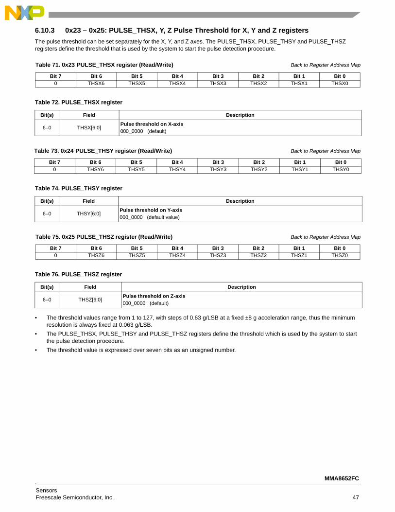
6.10.3 0x23 – 0x25: PULSE_THSX, Y, Z Pulse Threshold for X, Y and Z registers
The pulse threshold can be set separately for the X, Y, and Z axes. The PULSE_THSX, PULSE_THSY and PULSE_THSZ registers define the threshold that is used by the system to start the pulse detection procedure.
• The threshold values range from 1 to 127, with steps of 0.63 g/LSB at a fixed ±8 g acceleration range, thus the minimum resolution is always fixed at 0.063 g/LSB.
• The PULSE_THSX, PULSE_THSY and PULSE_THSZ registers define the threshold which is used by the system to start the pulse detection procedure.
• The threshold value is expressed over seven bits as an unsigned number.
Table 71. 0x23 PULSE_THSX register (Read/Write) Back to Register Address Map
Bit 7 Bit 6 Bit 5 Bit 4 Bit 3 Bit 2 Bit 1 Bit 00 THSX6 THSX5 THSX4 THSX3 THSX2 THSX1 THSX0
Table 72. PULSE_THSX register
Bit(s) Field Description
6–0 THSX[6:0]Pulse threshold on X-axis000_0000 (default)
Table 73. 0x24 PULSE_THSY register (Read/Write) Back to Register Address Map
Bit 7 Bit 6 Bit 5 Bit 4 Bit 3 Bit 2 Bit 1 Bit 00 THSY6 THSY5 THSY4 THSY3 THSY2 THSY1 THSY0
Table 74. PULSE_THSY register
Bit(s) Field Description
6–0 THSY[6:0]Pulse threshold on Y-axis000_0000 (default value)
Table 75. 0x25 PULSE_THSZ register (Read/Write) Back to Register Address Map
Bit 7 Bit 6 Bit 5 Bit 4 Bit 3 Bit 2 Bit 1 Bit 00 THSZ6 THSZ5 THSZ4 THSZ3 THSZ2 THSZ1 THSZ0
Table 76. PULSE_THSZ register
Bit(s) Field Description
6–0 THSZ[6:0]Pulse threshold on Z-axis000_0000 (default)
MMA8652FC
SensorsFreescale Semiconductor, Inc. 47
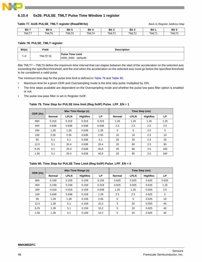
6.10.4 0x26: PULSE_TMLT Pulse Time Window 1 register
Bits TMLT7 – TMLT0 define the maximum time interval that can elapse between the start of the acceleration on the selected axis exceeding the specified threshold, and the end when the acceleration on the selected axis must go below the specified threshold to be considered a valid pulse.
The minimum time step for the pulse time limit is defined in Table 79 and Table 80.
• Maximum time for a given ODR and Oversampling mode is the time step pulse multiplied by 255.
• The time steps available are dependent on the Oversampling mode and whether the pulse low-pass filter option is enabled or not.
• The pulse low-pass filter is set in Register 0x0F.
Table 77. 0x26 PULSE_TMLT register (Read/Write) Back to Register Address Map
Bit 7 Bit 6 Bit 5 Bit 4 Bit 3 Bit 2 Bit 1 Bit 0TMLT7 TMLT6 TMLT5 TMLT4 TMLT3 TMLT2 TMLT1 TMLT0
Table 78. PULSE_TMLT register
Bit(s) Field Description
7–0 TMLT[7:0]Pulse Time Limit0000_0000 (default)
Table 79. Time Step for PULSE time limit (Reg 0x0F) Pulse_LPF_EN = 1
ODR (Hz)Max Time Range (s) Time Step (ms)
Normal LPLN HighRes LP Normal LPLN HighRes LP
800 0.319 0.319 0.319 0.319 1.25 1.25 1.25 1.25
400 0.638 0.638 0.638 0.638 2.5 2.5 2.5 2.5
200 1.28 1.28 0.638 1.28 5 5 2.5 5
100 2.55 2.55 0.638 2.55 10 10 2.5 10
50 5.1 5.1 0.638 5.1 20 20 2.5 20
12.5 5.1 20.4 0.638 20.4 20 80 2.5 80
6.25 5.1 20.4 0.638 40.8 20 80 2.5 160
1.56 5.1 20.4 0.638 40.8 20 80 2.5 160
Table 80. Time Step for PULSE Time Limit (Reg 0x0F) Pulse_LPF_EN = 0
ODR (Hz)Max Time Range (s) Time Step (ms)
Normal LPLN HighRes LP Normal LPLN HighRes LP
800 0.159 0.159 0.159 0.159 0.625 0.625 0.625 0.625
400 0.159 0.159 0.159 0.319 0.625 0.625 0.625 1.25
200 0.319 0.319 0.159 0.638 1.25 1.25 0.625 2.5
100 0.638 0.638 0.159 1.28 2.5 2.5 0.625 5
50 1.28 1.28 0.159 2.55 5 5 0.625 10
12.5 1.28 5.1 0.159 10.2 5 20 0.625 40
6.25 1.28 5.1 0.159 10.2 5 20 0.625 40
1.56 1.28 5.1 0.159 10.2 5 20 0.625 40
MMA8652FC
Sensors48 Freescale Semiconductor, Inc.
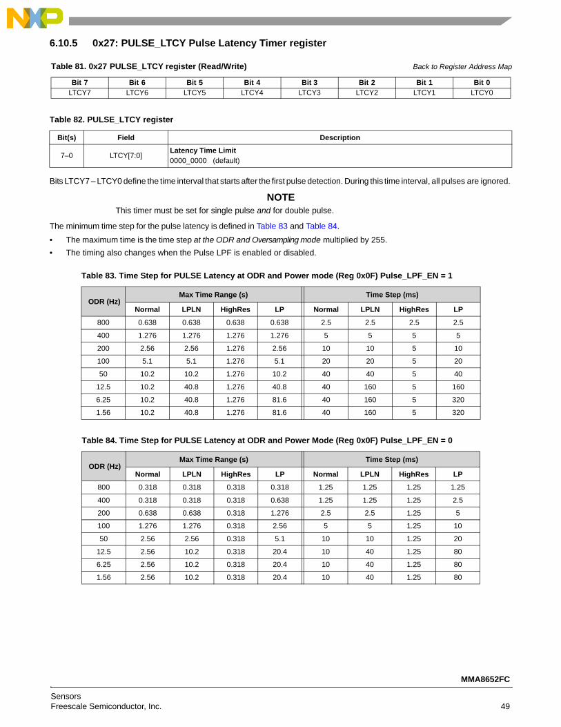
6.10.5 0x27: PULSE_LTCY Pulse Latency Timer register
Bits LTCY7 – LTCY0 define the time interval that starts after the first pulse detection. During this time interval, all pulses are ignored.
NOTEThis timer must be set for single pulse and for double pulse.
The minimum time step for the pulse latency is defined in Table 83 and Table 84.
• The maximum time is the time step at the ODR and Oversampling mode multiplied by 255.
• The timing also changes when the Pulse LPF is enabled or disabled.
Table 81. 0x27 PULSE_LTCY register (Read/Write) Back to Register Address Map
Bit 7 Bit 6 Bit 5 Bit 4 Bit 3 Bit 2 Bit 1 Bit 0LTCY7 LTCY6 LTCY5 LTCY4 LTCY3 LTCY2 LTCY1 LTCY0
Table 82. PULSE_LTCY register
Bit(s) Field Description
7–0 LTCY[7:0]Latency Time Limit0000_0000 (default)
Table 83. Time Step for PULSE Latency at ODR and Power mode (Reg 0x0F) Pulse_LPF_EN = 1
ODR (Hz)Max Time Range (s) Time Step (ms)
Normal LPLN HighRes LP Normal LPLN HighRes LP
800 0.638 0.638 0.638 0.638 2.5 2.5 2.5 2.5
400 1.276 1.276 1.276 1.276 5 5 5 5
200 2.56 2.56 1.276 2.56 10 10 5 10
100 5.1 5.1 1.276 5.1 20 20 5 20
50 10.2 10.2 1.276 10.2 40 40 5 40
12.5 10.2 40.8 1.276 40.8 40 160 5 160
6.25 10.2 40.8 1.276 81.6 40 160 5 320
1.56 10.2 40.8 1.276 81.6 40 160 5 320
Table 84. Time Step for PULSE Latency at ODR and Power Mode (Reg 0x0F) Pulse_LPF_EN = 0
ODR (Hz)Max Time Range (s) Time Step (ms)
Normal LPLN HighRes LP Normal LPLN HighRes LP
800 0.318 0.318 0.318 0.318 1.25 1.25 1.25 1.25
400 0.318 0.318 0.318 0.638 1.25 1.25 1.25 2.5
200 0.638 0.638 0.318 1.276 2.5 2.5 1.25 5
100 1.276 1.276 0.318 2.56 5 5 1.25 10
50 2.56 2.56 0.318 5.1 10 10 1.25 20
12.5 2.56 10.2 0.318 20.4 10 40 1.25 80
6.25 2.56 10.2 0.318 20.4 10 40 1.25 80
1.56 2.56 10.2 0.318 20.4 10 40 1.25 80
MMA8652FC
SensorsFreescale Semiconductor, Inc. 49
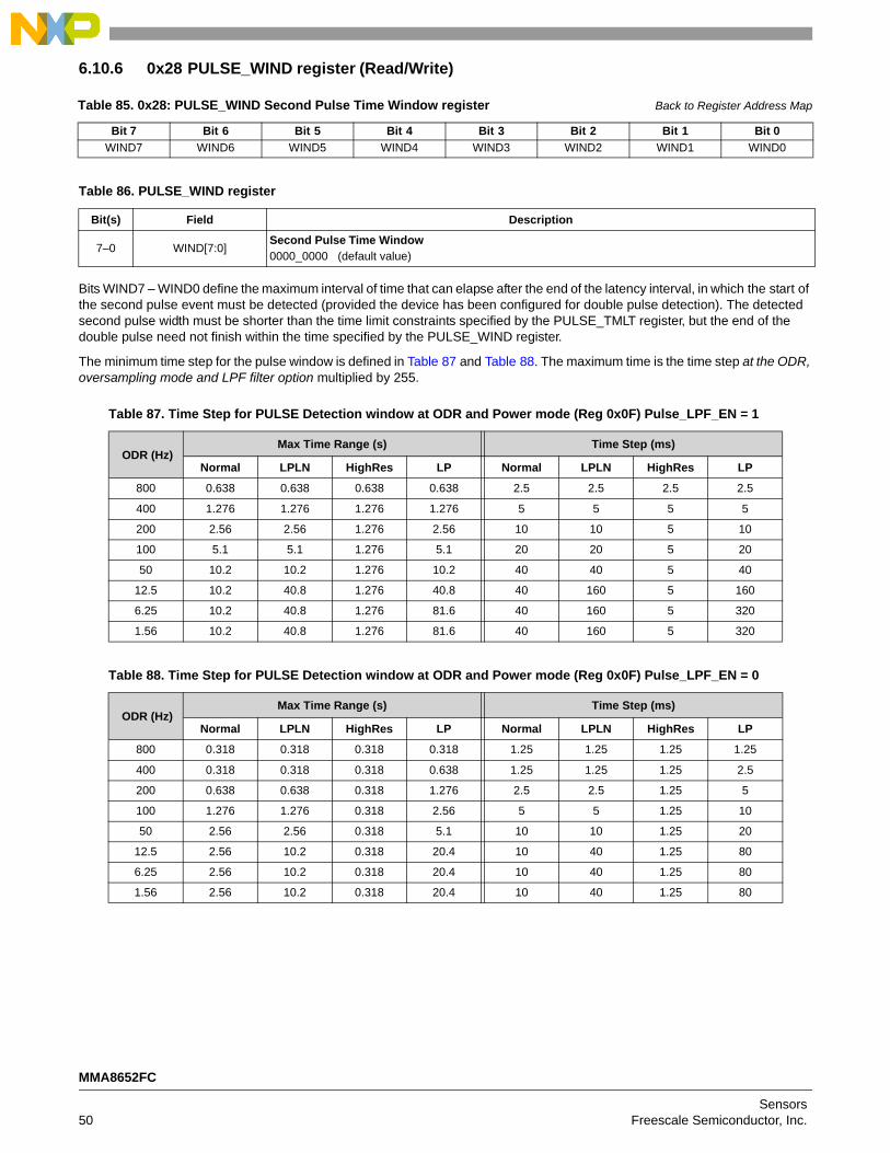
6.10.6 0x28 PULSE_WIND register (Read/Write)
Bits WIND7 – WIND0 define the maximum interval of time that can elapse after the end of the latency interval, in which the start of the second pulse event must be detected (provided the device has been configured for double pulse detection). The detected second pulse width must be shorter than the time limit constraints specified by the PULSE_TMLT register, but the end of the double pulse need not finish within the time specified by the PULSE_WIND register.
The minimum time step for the pulse window is defined in Table 87 and Table 88. The maximum time is the time step at the ODR, oversampling mode and LPF filter option multiplied by 255.
Table 85. 0x28: PULSE_WIND Second Pulse Time Window register Back to Register Address Map
Bit 7 Bit 6 Bit 5 Bit 4 Bit 3 Bit 2 Bit 1 Bit 0
WIND7 WIND6 WIND5 WIND4 WIND3 WIND2 WIND1 WIND0
Table 86. PULSE_WIND register
Bit(s) Field Description
7–0 WIND[7:0]Second Pulse Time Window0000_0000 (default value)
Table 87. Time Step for PULSE Detection window at ODR and Power mode (Reg 0x0F) Pulse_LPF_EN = 1
ODR (Hz)Max Time Range (s) Time Step (ms)
Normal LPLN HighRes LP Normal LPLN HighRes LP
800 0.638 0.638 0.638 0.638 2.5 2.5 2.5 2.5
400 1.276 1.276 1.276 1.276 5 5 5 5
200 2.56 2.56 1.276 2.56 10 10 5 10
100 5.1 5.1 1.276 5.1 20 20 5 20
50 10.2 10.2 1.276 10.2 40 40 5 40
12.5 10.2 40.8 1.276 40.8 40 160 5 160
6.25 10.2 40.8 1.276 81.6 40 160 5 320
1.56 10.2 40.8 1.276 81.6 40 160 5 320
Table 88. Time Step for PULSE Detection window at ODR and Power mode (Reg 0x0F) Pulse_LPF_EN = 0
ODR (Hz)Max Time Range (s) Time Step (ms)
Normal LPLN HighRes LP Normal LPLN HighRes LP
800 0.318 0.318 0.318 0.318 1.25 1.25 1.25 1.25
400 0.318 0.318 0.318 0.638 1.25 1.25 1.25 2.5
200 0.638 0.638 0.318 1.276 2.5 2.5 1.25 5
100 1.276 1.276 0.318 2.56 5 5 1.25 10
50 2.56 2.56 0.318 5.1 10 10 1.25 20
12.5 2.56 10.2 0.318 20.4 10 40 1.25 80
6.25 2.56 10.2 0.318 20.4 10 40 1.25 80
1.56 2.56 10.2 0.318 20.4 10 40 1.25 80
MMA8652FC
Sensors50 Freescale Semiconductor, Inc.
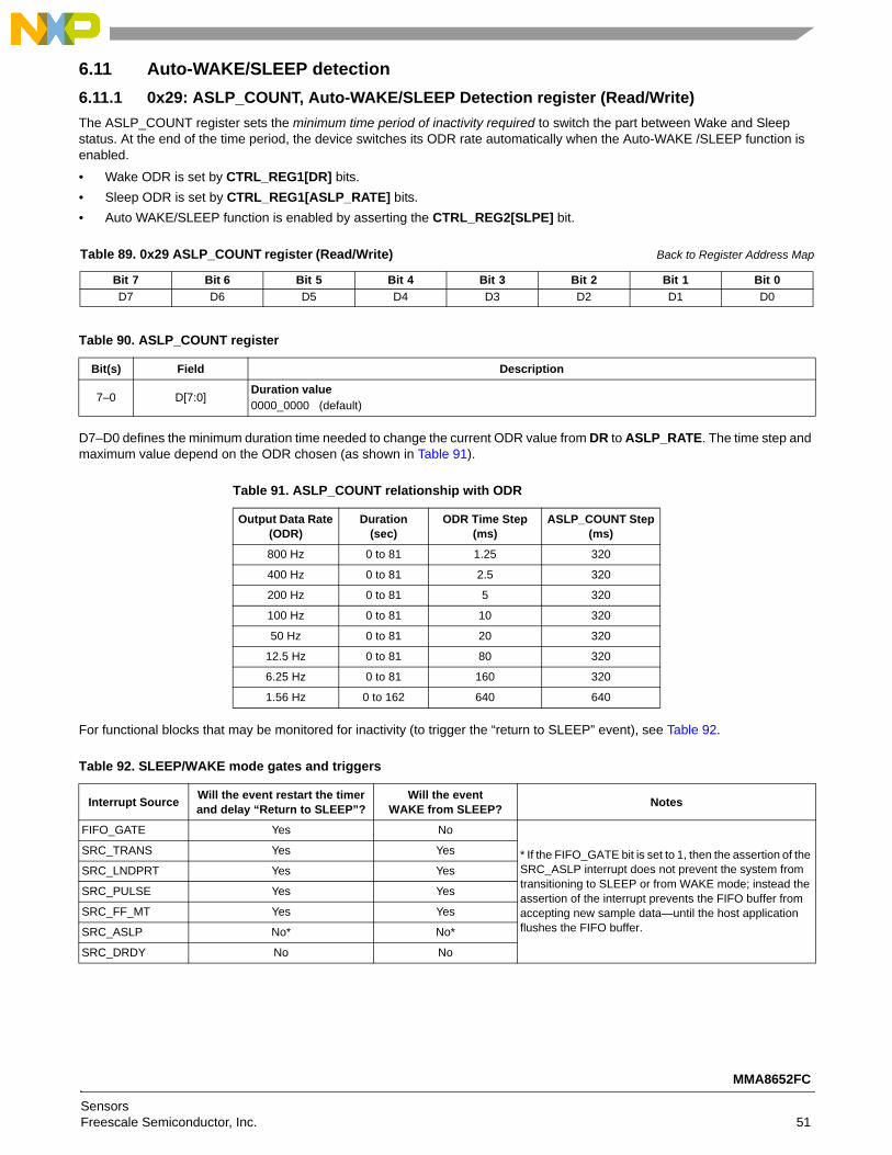
6.11 Auto-WAKE/SLEEP detection
6.11.1 0x29: ASLP_COUNT, Auto-WAKE/SLEEP Detection register (Read/Write)
The ASLP_COUNT register sets the minimum time period of inactivity required to switch the part between Wake and Sleep status. At the end of the time period, the device switches its ODR rate automatically when the Auto-WAKE /SLEEP function is enabled.
• Wake ODR is set by CTRL_REG1[DR] bits.
• Sleep ODR is set by CTRL_REG1[ASLP_RATE] bits.
• Auto WAKE/SLEEP function is enabled by asserting the CTRL_REG2[SLPE] bit.
D7–D0 defines the minimum duration time needed to change the current ODR value from DR to ASLP_RATE. The time step and maximum value depend on the ODR chosen (as shown in Table 91).
For functional blocks that may be monitored for inactivity (to trigger the “return to SLEEP” event), see Table 92.
Table 89. 0x29 ASLP_COUNT register (Read/Write) Back to Register Address Map
Bit 7 Bit 6 Bit 5 Bit 4 Bit 3 Bit 2 Bit 1 Bit 0
D7 D6 D5 D4 D3 D2 D1 D0
Table 90. ASLP_COUNT register
Bit(s) Field Description
7–0 D[7:0]Duration value0000_0000 (default)
Table 91. ASLP_COUNT relationship with ODR
Output Data Rate (ODR)
Duration(sec)
ODR Time Step (ms)
ASLP_COUNT Step (ms)
800 Hz 0 to 81 1.25 320
400 Hz 0 to 81 2.5 320
200 Hz 0 to 81 5 320
100 Hz 0 to 81 10 320
50 Hz 0 to 81 20 320
12.5 Hz 0 to 81 80 320
6.25 Hz 0 to 81 160 320
1.56 Hz 0 to 162 640 640
Table 92. SLEEP/WAKE mode gates and triggers
Interrupt SourceWill the event restart the timer and delay “Return to SLEEP”?
Will the event WAKE from SLEEP?
Notes
FIFO_GATE Yes No
* If the FIFO_GATE bit is set to 1, then the assertion of the SRC_ASLP interrupt does not prevent the system from transitioning to SLEEP or from WAKE mode; instead the assertion of the interrupt prevents the FIFO buffer from accepting new sample data—until the host application flushes the FIFO buffer.
SRC_TRANS Yes Yes
SRC_LNDPRT Yes Yes
SRC_PULSE Yes Yes
SRC_FF_MT Yes Yes
SRC_ASLP No* No*
SRC_DRDY No No
MMA8652FC
SensorsFreescale Semiconductor, Inc. 51
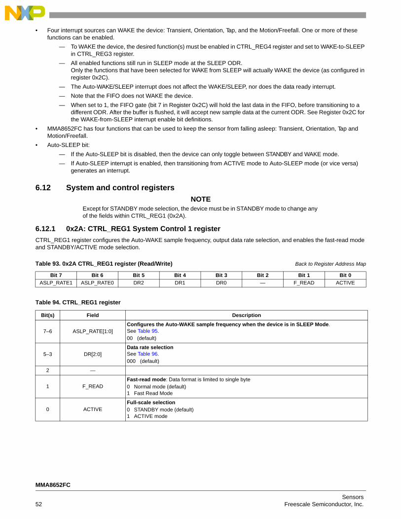
• Four interrupt sources can WAKE the device: Transient, Orientation, Tap, and the Motion/Freefall. One or more of these functions can be enabled.
— To WAKE the device, the desired function(s) must be enabled in CTRL_REG4 register and set to WAKE-to-SLEEP in CTRL_REG3 register.
— All enabled functions still run in SLEEP mode at the SLEEP ODR. Only the functions that have been selected for WAKE from SLEEP will actually WAKE the device (as configured in register 0x2C).
— The Auto-WAKE/SLEEP interrupt does not affect the WAKE/SLEEP, nor does the data ready interrupt.
— Note that the FIFO does not WAKE the device.
— When set to 1, the FIFO gate (bit 7 in Register 0x2C) will hold the last data in the FIFO, before transitioning to a different ODR. After the buffer is flushed, it will accept new sample data at the current ODR. See Register 0x2C for the WAKE-from-SLEEP interrupt enable bit definitions.
• MMA8652FC has four functions that can be used to keep the sensor from falling asleep: Transient, Orientation, Tap and Motion/Freefall.
• Auto-SLEEP bit:
— If the Auto-SLEEP bit is disabled, then the device can only toggle between STANDBY and WAKE mode.
— If Auto-SLEEP interrupt is enabled, then transitioning from ACTIVE mode to Auto-SLEEP mode (or vice versa) generates an interrupt.
6.12 System and control registers
NOTEExcept for STANDBY mode selection, the device must be in STANDBY mode to change any of the fields within CTRL_REG1 (0x2A).
6.12.1 0x2A: CTRL_REG1 System Control 1 register
CTRL_REG1 register configures the Auto-WAKE sample frequency, output data rate selection, and enables the fast-read mode and STANDBY/ACTIVE mode selection.
Table 93. 0x2A CTRL_REG1 register (Read/Write) Back to Register Address Map
Bit 7 Bit 6 Bit 5 Bit 4 Bit 3 Bit 2 Bit 1 Bit 0
ASLP_RATE1 ASLP_RATE0 DR2 DR1 DR0 — F_READ ACTIVE
Table 94. CTRL_REG1 register
Bit(s) Field Description
7–6 ASLP_RATE[1:0]Configures the Auto-WAKE sample frequency when the device is in SLEEP Mode. See Table 95.00 (default)
5–3 DR[2:0]Data rate selection See Table 96.000 (default)
2 —
1 F_READFast-read mode: Data format is limited to single byte0 Normal mode (default)1 Fast Read Mode
0 ACTIVEFull-scale selection0 STANDBY mode (default) 1 ACTIVE mode
MMA8652FC
Sensors52 Freescale Semiconductor, Inc.
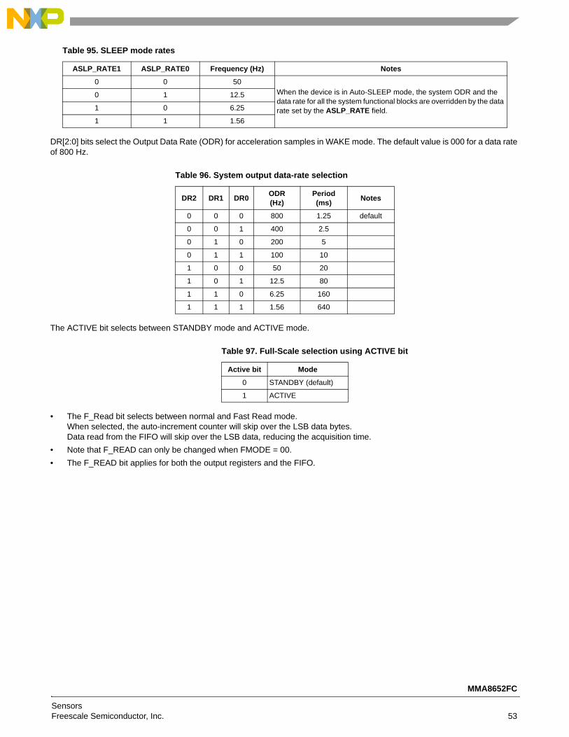
DR[2:0] bits select the Output Data Rate (ODR) for acceleration samples in WAKE mode. The default value is 000 for a data rate of 800 Hz.
The ACTIVE bit selects between STANDBY mode and ACTIVE mode.
• The F_Read bit selects between normal and Fast Read mode. When selected, the auto-increment counter will skip over the LSB data bytes. Data read from the FIFO will skip over the LSB data, reducing the acquisition time.
• Note that F_READ can only be changed when FMODE = 00.
• The F_READ bit applies for both the output registers and the FIFO.
Table 95. SLEEP mode rates
ASLP_RATE1 ASLP_RATE0 Frequency (Hz) Notes
0 0 50When the device is in Auto-SLEEP mode, the system ODR and the data rate for all the system functional blocks are overridden by the data rate set by the ASLP_RATE field.
0 1 12.5
1 0 6.25
1 1 1.56
Table 96. System output data-rate selection
DR2 DR1 DR0ODR(Hz)
Period(ms)
Notes
0 0 0 800 1.25 default
0 0 1 400 2.5
0 1 0 200 5
0 1 1 100 10
1 0 0 50 20
1 0 1 12.5 80
1 1 0 6.25 160
1 1 1 1.56 640
Table 97. Full-Scale selection using ACTIVE bit
Active bit Mode
0 STANDBY (default)
1 ACTIVE
MMA8652FC
SensorsFreescale Semiconductor, Inc. 53
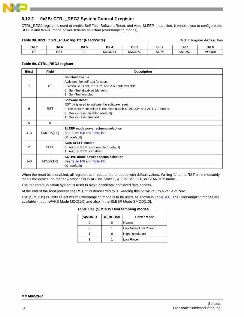
6.12.2 0x2B: CTRL_REG2 System Control 2 register
CTRL_REG2 register is used to enable Self-Test, Software Reset, and Auto-SLEEP. In addition, it enables you to configure the SLEEP and WAKE mode power scheme selection (oversampling modes).
When the reset bit is enabled, all registers are reset and are loaded with default values. Writing ‘1’ to the RST bit immediately resets the device, no matter whether it is in ACTIVE/WAKE, ACTIVE/SLEEP, or STANDBY mode.
The I2C communication system is reset to avoid accidental corrupted data access.
At the end of the boot process the RST bit is deasserted to 0. Reading this bit will return a value of zero.
The (S)MODS[1:0] bits select which Oversampling mode is to be used, as shown in Table 100. The Oversampling modes are available in both WAKE Mode MOD[1:0] and also in the SLEEP Mode SMOD[1:0].
Table 98. 0x2B CTRL_REG2 register (Read/Write) Back to Register Address Map
Bit 7 Bit 6 Bit 5 Bit 4 Bit 3 Bit 2 Bit 1 Bit 0
ST RST 0 SMODS1 SMODS0 SLPE MODS1 MODS0
Table 99. CTRL_REG2 register
Bit(s) Field Description
7 ST
Self-Test EnableActivates the self-test function. • When ST is set, the X, Y, and Z outputs will shift. 0 Self-Test disabled (default)1 Self-Test enabled
6 RST
Software ResetRST bit is used to activate the software reset.• The reset mechanism is enabled in both STANDBY and ACTIVE modes.0 Device reset disabled (default)1 Device reset enabled.
5 0
4–3 SMODS[1:0]SLEEP mode power scheme selectionSee Table 100 and Table 10100 (default)
2 SLPEAuto-SLEEP enable0 Auto-SLEEP is not enabled (default)1 Auto-SLEEP is enabled.
1–0 MODS[1:0]ACTIVE mode power scheme selectionSee Table 100 and Table 10100 (default)
Table 100. (S)MODS Oversampling modes
(S)MODS1 (S)MODS0 Power Mode
0 0 Normal
0 1 Low Noise Low Power
1 0 High Resolution
1 1 Low Power
MMA8652FC
Sensors54 Freescale Semiconductor, Inc.
6.12.3 0x2C: CTRL_REG3 Interrupt Control register
CTRL_REG3 register is used to control the Auto-WAKE/SLEEP function by setting the orientation or Freefall/Motion as an interrupt to wake. CTRL_REG3 register also configures the interrupt pins INT1 and INT2.
Table 101. MODS Oversampling modes averaging values at each ODR
ODR (Hz)
Mode
Normal (00) Low Noise Low Power (01) High Resolution (10) Low Power (11)
Current μA OS Ratio Current μA OS Ratio Current μA OS Ratio Current μA OS Ratio
1.56 27 128 9 32 184 1024 6.5 16
6.25 27 32 9 8 184 256 6.5 4
12.5 27 16 9 4 184 128 6.5 2
50 27 4 27 4 184 32 15 2
100 49 4 49 4 184 16 26 2
200 94 4 94 4 184 8 49 2
400 184 4 184 4 184 4 94 2
800 184 2 184 2 184 2 184 2
Table 102. 0x2C CTRL_REG3 register (Read/Write) Back to Register Address Map
Bit 7 Bit 6 Bit 5 Bit 4 Bit 3 Bit 2 Bit 1 Bit 0FIFO_GATE WAKE_TRANS WAKE_LNDPRT WAKE_PULSE WAKE_FF_MT 0 IPOL PP_OD
Table 103. CTRL_REG3 register
Bit(s) Field Description
7 FIFO_GATE
FIFO Gate 0 FIFO gate is bypassed. (default)
FIFO is flushed upon the system mode transitioning from WAKE to SLEEP mode or from SLEEP to WAKE mode.
1 The FIFO input buffer is blocked when transitioning from WAKE to SLEEP mode or from SLEEP to WAKE mode, until the FIFO is flushed. Although the system transitions from WAKE to SLEEP or from SLEEP to WAKE—the contents of the FIFO buffer are preserved, and new data samples are ignored until the FIFO is emptied by the host application.If the FIFO_GATE bit is set to 1 and the FIFO buffer is not emptied before the arrival of the next sample, then the FGERR bit in the SYS_MOD register (0x0B) will be asserted. The FGERR bit remains asserted as long as the FIFO buffer remains un-emptied. Emptying the FIFO buffer clears the FGERR bit in the SYS_MOD register.
6 WAKE_TRANSWake from Transient interrupt 0 Transient function is bypassed in SLEEP mode. (default)1 Transient function interrupt can wake up system
5 WAKE_LNDPRTWake from Orientation interrupt 0 Orientation function is bypassed in SLEEP mode. (default)1 Orientation function interrupt can wake up system
4 WAKE_PULSEWake from Pulse interrupt0 Pulse function is bypassed in SLEEP mode. (default)1 Pulse function interrupt can wake up system
3 WAKE_FF_MTWake from Freefall/Motion interrupt 0 Freefall/Motion function is bypassed in SLEEP mode. (default)1 Freefall/Motion function interrupt can wake up
2 0
1 IPOL
Interrupt polarity Selects the polarity of the interrupt signals. When IPOL is 0 (default value), any interrupt event is signaled with a logical 0.0 ACTIVE low (default)1 ACTIVE high
MMA8652FC
SensorsFreescale Semiconductor, Inc. 55
6.12.4 0x2D: CTRL_REG4 Interrupt Enable register (Read/Write)
CTRL_REG4 register enables the following interrupts: Auto-WAKE/SLEEP, Orientation Detection, Freefall/Motion, and Data Ready.
6.12.5 0x2E CTRL_REG5 Interrupt Configuration register (Read/Write)
CTRL_REG5 register maps the desired interrupts to INT2 or INT1 pins.
The system’s interrupt controller, shown in Figure 9, uses the corresponding bit field in the CTRL_REG5 register to determine the routing table for the INT1 and INT2 interrupt pins.
• If the bit value is 0, then the functional block’s interrupt is routed to INT2.
• If the bit value is 1, then the functional block’s interrupt is routed to INT1.
One or more functions can assert an interrupt pin; therefore a host application responding to an interrupt should read the INT_SOURCE (0x0C) register, to determine the appropriate sources of the interrupt.
0 PP_OD
Push-Pull/Open-Drain selection on interrupt padConfigures the interrupt pins to Push-Pull or to Open-Drain mode. The Open-Drain configuration can be used for connecting multiple interrupt signals on the same interrupt line.0 Push-Pull (default)1 Open Drain
Table 104. 0x2D CTRL_REG4 Interrupt Enable register (Read/Write) Back to Register Address Map
Bit 7 Bit 6 Bit 5 Bit 4 Bit 3 Bit 2 Bit 1 Bit 0INT_EN_ASLP INT_EN_FIFO INT_EN_TRANS INT_EN_LNDPRT INT_EN_PULSE INT_EN_FF_MT 0 INT_EN_DRDY
Table 105. CTRL_REG4 register
Bit(s) Field Description7 INT_EN_ASLP Auto-SLEEP/WAKE Interrupt Enable 0 interrupt is disabled (default)
1 interrupt is enabled
Note: The corresponding functional block interrupt enable bit enables the functional block to route its event detection flags to the system’s interrupt controller. The interrupt controller routes the enabled functional block interrupt to the INT1 or INT2 pin.
6 INT_EN_FIFO FIFO Interrupt Enable
5 INT_EN_TRANS Transient Interrupt Enable
4 INT_EN_LNDPRT Orientation (Landscape/Portrait) Interrupt Enable
3 INT_EN_PULSE Pulse Detection Interrupt Enable
2 INT_EN_FF_MT Freefall/Motion Interrupt Enable
0 INT_EN_DRDY Data Ready Interrupt Enable
Table 106. 0x2E: CTRL_REG5 Interrupt Configuration register Back to Register Address Map
Bit 7 Bit 6 Bit 5 Bit 4 Bit 3 Bit 2 Bit 1 Bit 0
INT_CFG_ASLP INT_CFG_FIFO INT_CFG_TRANS INT_CFG_LNDPRT INT_CFG_PULSE INT_CFG_FF_MT 0 INT_CFG_DRDY
Table 107. 0x2E CTRL_REG5 register
Bit(s) Field Description
7 INT_CFG_ASLP Auto-SLEEP/WAKE INT1/INT2 Configuration
0 Interrupt is routed to INT2 pin (default)1 Interrupt is routed to INT1 pin
6 INT_CFG_FIFO FIFO INT1/INT2 Configuration
5 INT_CFG_TRANS Transient INT1/INT2 Configuration
4 INT_CFG_LNDPRT Orientation INT1/INT2 Configuration
3 INT_CFG_PULSE Pulse INT1/INT2 Configuration
2 INT_CFG_FF_MT Freefall/motion INT1/INT2 Configuration
1 0
0 INT_CFG_DRDY Data Ready INT1/INT2 Configuration
Table 103. CTRL_REG3 register (Continued)
MMA8652FC
Sensors56 Freescale Semiconductor, Inc.
6.13 Data calibration registersThe 2’s complement offset correction registers values are used to realign the Zero-g position of the X, Y, and Z-axis after the device is mounted on a board. The resolution of the offset registers is 1.96 mg/LSB. The 2’s complement 8-bit value would result in an offset compensation range ±250 mg for each axis.
6.13.1 0x2F: OFF_X Offset Correction X register
6.13.2 0x30: OFF_Y Offset Correction Y register
6.13.3 0x31: OFF_Z Offset Correction Z register
Table 108. 0x2F OFF_X register (Read/Write) Back to Register Address Map
Bit 7 Bit 6 Bit 5 Bit 4 Bit 3 Bit 2 Bit 1 Bit 0
D7 D6 D5 D4 D3 D2 D1 D0
Table 109. OFF_X register
Bit(s) Field Description
7–0 D[7:0]X-axis offset value0000_0000 (default)
Table 110. 0x30 OFF_Y register (Read/Write) Back to Register Address Map
Bit 7 Bit 6 Bit 5 Bit 4 Bit 3 Bit 2 Bit 1 Bit 0
D7 D6 D5 D4 D3 D2 D1 D0
Table 111. OFF_Y register
Bit(s) Field Description
7–0 D[7:0]Y-axis offset value0000_0000 (default)
Table 112. 0x31 OFF_Z register (Read/Write) Back to Register Address Map
Bit 7 Bit 6 Bit 5 Bit 4 Bit 3 Bit 2 Bit 1 Bit 0
D7 D6 D5 D4 D3 D2 D1 D0
Table 113. OFF_Z register
Bit(s) Field Description
7–0 D[7:0]Z-axis offset value0000_0000 (default)
MMA8652FC
SensorsFreescale Semiconductor, Inc. 57

7 Mounting GuidelinesSurface mount printed circuit board (PCB) layout is a critical portion of the total design. The footprint for the surface mount packages must be the correct size to ensure proper solder connection interface between the PCB and the package. With the correct footprint, the packages will self-align when subjected to a solder reflow process. These guidelines are for soldering and mounting the Dual Flat No-Lead (DFN) package inertial sensors to PCBs. The purpose is to minimize the stress on the package after board mounting. The MMA865xFC digital output accelerometers use the DFN package platform. This section describes suggested methods of soldering these devices to the PCB for consumer applications.
7.1 Overview of soldering considerationsInformation provided here is based on experiments executed on DFN devices. They do not represent exact conditions present at a customer site. Therefore, this information should be used as guidance only and process and design optimizations are recommended to develop an application specific solution. It should be noted that with the proper PCB footprint and solder stencil designs, the package will self-align during the solder reflow process.
7.2 Halogen contentThis package is designed to be Halogen Free, exceeding most industry and customer standards. Halogen Free means that no homogeneous material within the assembly package shall contain chlorine (Cl) in excess of 700 ppm or 0.07% weight/weight or bromine (Br) in excess of 900 ppm or 0.09% weight/weight.
7.3 PCB mounting/soldering recommendations1. The PCB land should be designed as Non Solder Mask Defined (NSMD) as shown in Figure 16.2. No additional via pattern underneath package.3. PCB land pad is 0.6 mm x 0.225 mm as shown in Figure 16.4. Solder mask opening = PCB land pad edge + 0.125 mm larger all around = 0.725 mm x 1.950 mm5. Stencil opening = PCB land pad – 0.05 mm smaller all around = 0.55 mm x 0.175 mm.6. Stencil thickness is 100 or 125 µm.7. Do not place any components or vias at a distance less than 2 mm from the package land area. This may cause
additional package stress if it is too close to the package land area.8. Signal traces connected to pads are as symmetric as possible. Put dummy traces on NC pads, to have same length of
exposed trace for all pads.9. Use a standard pick and place process and equipment. Do not use a hand soldering process.10. Use caution when putting an assembled PCB into an enclosure, noting where the screw-down holes are and if any
press-fitting is involved. It is important that the assembled PCB remain flat after assembly, to ensure optimal electronic operation of the device.
11. The PCB should be rated for the multiple lead-free reflow condition with max 260°C temperature.12. No copper traces on top layer of PCB under the package. This will cause planarity issues with board mount. Freescale
DFN sensors are compliant with Restrictions on Hazardous Substances (RoHS), having halide free molding compound (green) and lead-free terminations. These terminations are compatible with tin-lead (Sn-Pb) as well as tin-silver-copper (Sn-Ag-Cu) solder paste soldering processes. Reflow profiles applicable to those processes can be used successfully for soldering the devices.
MMA8652FC
Sensors58 Freescale Semiconductor, Inc.
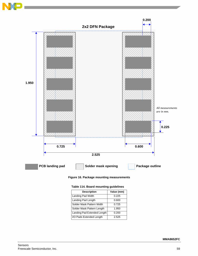
Figure 16. Package mounting measurements
Table 114. Board mounting guidelines
Description Value (mm)
Landing Pad Width 0.225
Landing Pad Length 0.600
Solder Mask Pattern Width 0.725
Solder Mask Pattern Length 1.950
Landing Pad Extended Length 0.200
I/O Pads Extended Length 2.525
0.225
0.200
0.600
1.950
0.725
Solder mask openingPCB landing pad
2x2 DFN Package
All measurements are in mm.
Package outline
2.525
MMA8652FC
SensorsFreescale Semiconductor, Inc. 59
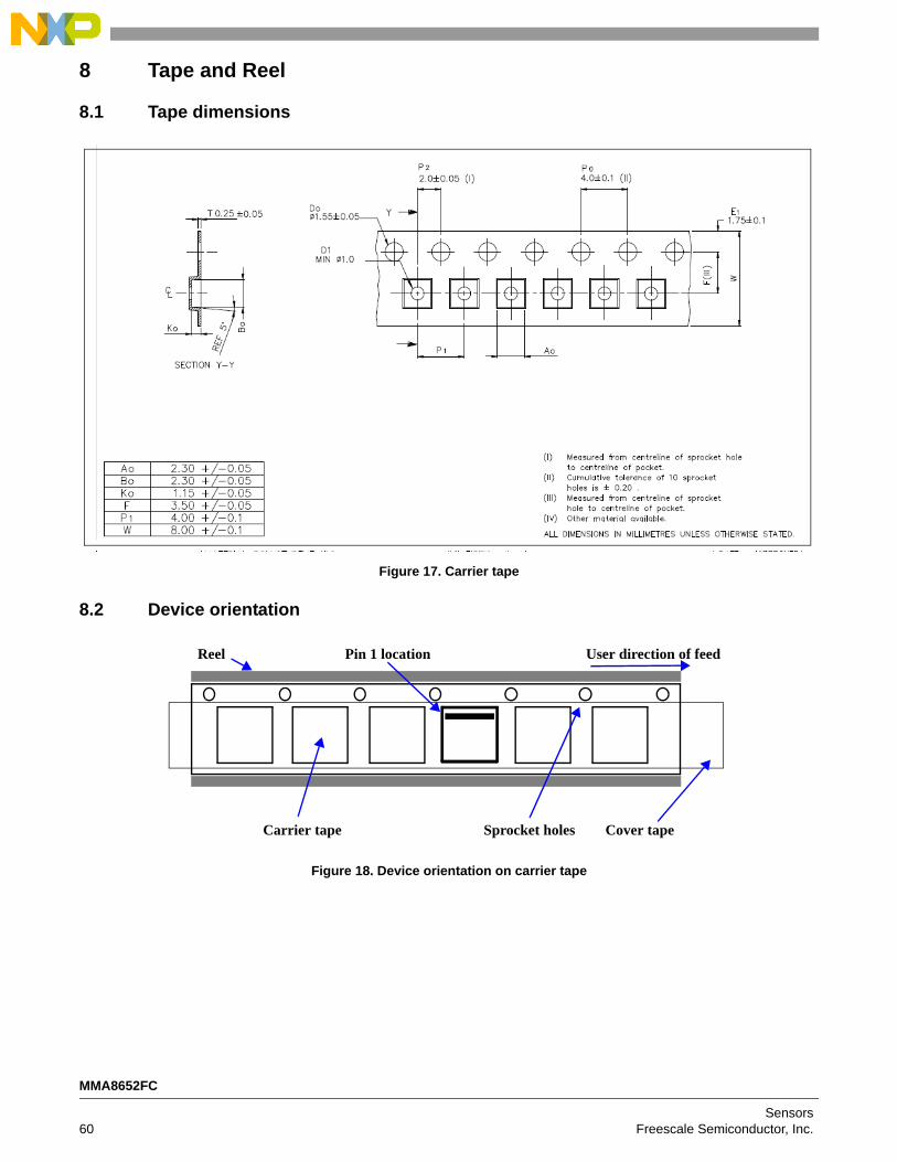
8 Tape and Reel
8.1 Tape dimensions
Figure 17. Carrier tape
8.2 Device orientation
Figure 18. Device orientation on carrier tape
Reel
Carrier tape
Pin 1 location
Sprocket holes Cover tape
User direction of feed
MMA8652FC
Sensors60 Freescale Semiconductor, Inc.
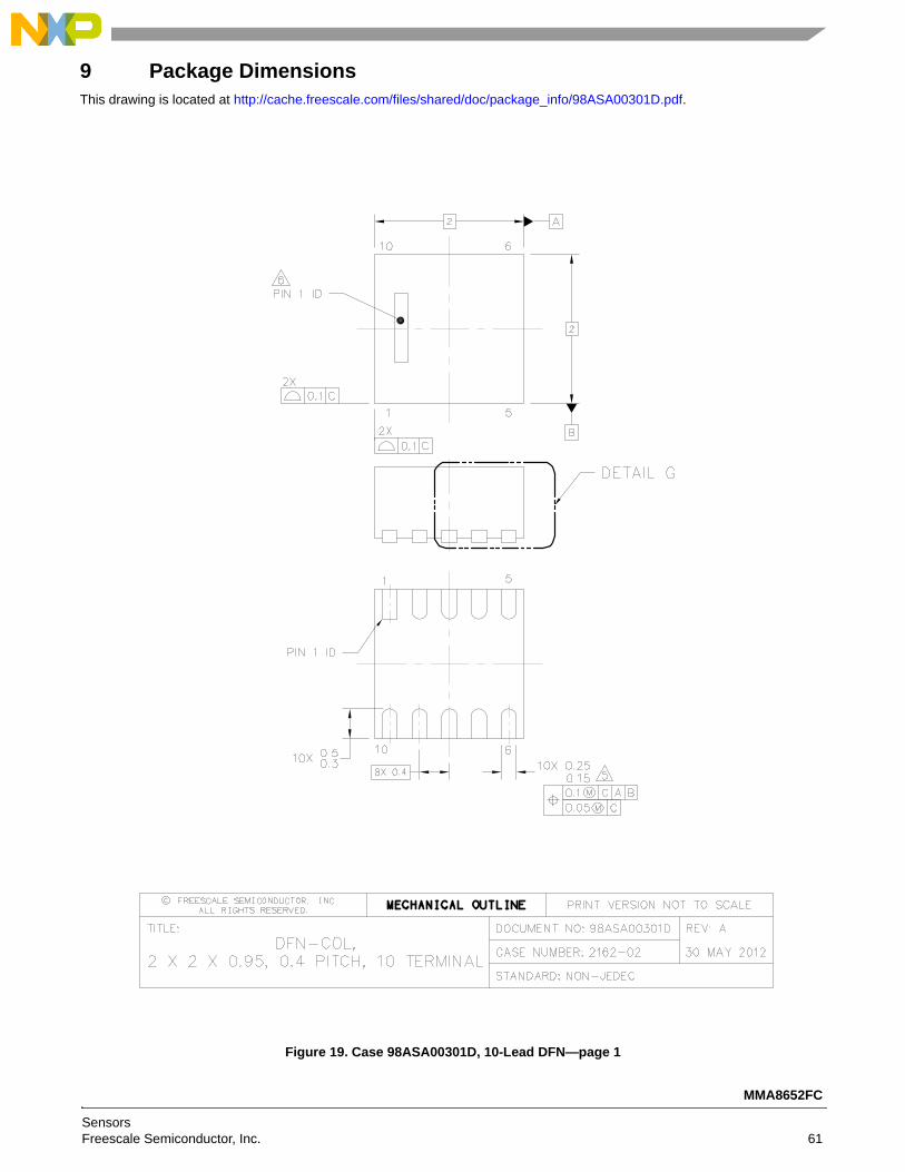
9 Package DimensionsThis drawing is located at http://cache.freescale.com/files/shared/doc/package_info/98ASA00301D.pdf.
Figure 19. Case 98ASA00301D, 10-Lead DFN—page 1
MMA8652FC
SensorsFreescale Semiconductor, Inc. 61
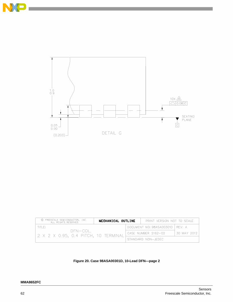
Figure 20. Case 98ASA00301D, 10-Lead DFN—page 2
MMA8652FC
Sensors62 Freescale Semiconductor, Inc.
Figure 21. Case 98ASA00301D, 10-Lead DFN—page 3
MMA8652FC
SensorsFreescale Semiconductor, Inc. 63
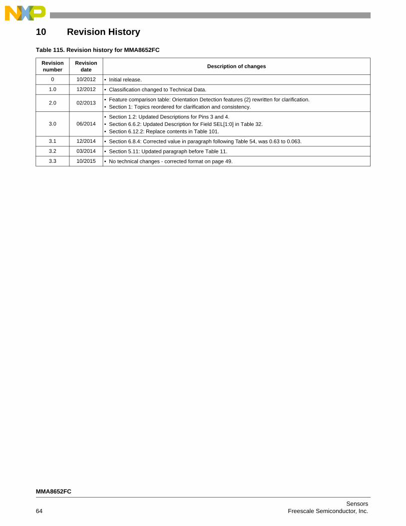
10 Revision History
Table 115. Revision history for MMA8652FC
Revision number
Revision date
Description of changes
0 10/2012 • Initial release.
1.0 12/2012 • Classification changed to Technical Data.
2.0 02/2013• Feature comparison table: Orientation Detection features (2) rewritten for clarification.• Section 1: Topics reordered for clarification and consistency.
3.0 06/2014• Section 1.2: Updated Descriptions for Pins 3 and 4.• Section 6.6.2: Updated Description for Field SEL[1:0] in Table 32.• Section 6.12.2: Replace contents in Table 101.
3.1 12/2014 • Section 6.8.4: Corrected value in paragraph following Table 54, was 0.63 to 0.063.
3.2 03/2014 • Section 5.11: Updated paragraph before Table 11.
3.3 10/2015 • No technical changes - corrected format on page 49.
MMA8652FC
Sensors64 Freescale Semiconductor, Inc.
Document Number: MMA8652FCRev. 3.310/2015
Information in this document is provided solely to enable system and software
implementers to use Freescale products. There are no express or implied copyright
licenses granted hereunder to design or fabricate any integrated circuits based on the
information in this document.
Freescale reserves the right to make changes without further notice to any products
herein. Freescale makes no warranty, representation, or guarantee regarding the
suitability of its products for any particular purpose, nor does Freescale assume any
liability arising out of the application or use of any product or circuit, and specifically
disclaims any and all liability, including without limitation consequential or incidental
damages. “Typical” parameters that may be provided in Freescale data sheets and/or
specifications can and do vary in different applications, and actual performance may
vary over time. All operating parameters, including “typicals,” must be validated for each
customer application by customer’s technical experts. Freescale does not convey any
license under its patent rights nor the rights of others. Freescale sells products pursuant
to standard terms and conditions of sale, which can be found at the following address:
freescale.com/salestermsandconditions.
How to Reach Us:
Home Page: freescale.com
Web Support: freescale.com/support
Freescale and the Freescale logo are trademarks of Freescale Semiconductor, Inc.,
Reg. U.S. Pat. & Tm. Off. All other product or service names are the property of their
respective owners.
© 2015 Freescale Semiconductor, Inc.