Embed Size (px)
Citation preview
MLX90314 Programmable Sensor Interface
3901090314 Rev 008
Page 1 Apr/12
Features and Benefits Microprocessor-controlled signal conditioning for bridge-type sensors Suited for low-cost sensors: reduction of non-linearity by programmable coefficients External or internal temperature sensor for compensating temperature errors Versatile output signal ranges: 4, 5, 10, or 11VDC; 4 to 20 mA loop Mass calibration easy with 2400 or 9600 baud UART Power supply from 6 to 35VDC
Applications Pressure transducers Accelerometers Temperature sensor assemblies Linear position sensors
Ordering Code Product Code Temperature Code Package Code Option Code Packing Form Code
MLX90314 L DF BAA-000 TU MLX90314 L DF BAA-000 RE
Legend: Temperature Code: L for Temperature Range -40°C to 150°C
Package Code: DF for SOIC300Mil
Packing Form: RE for Reel, TU for Tube Ordering example: MLX90314LDF-BAA-000-TU
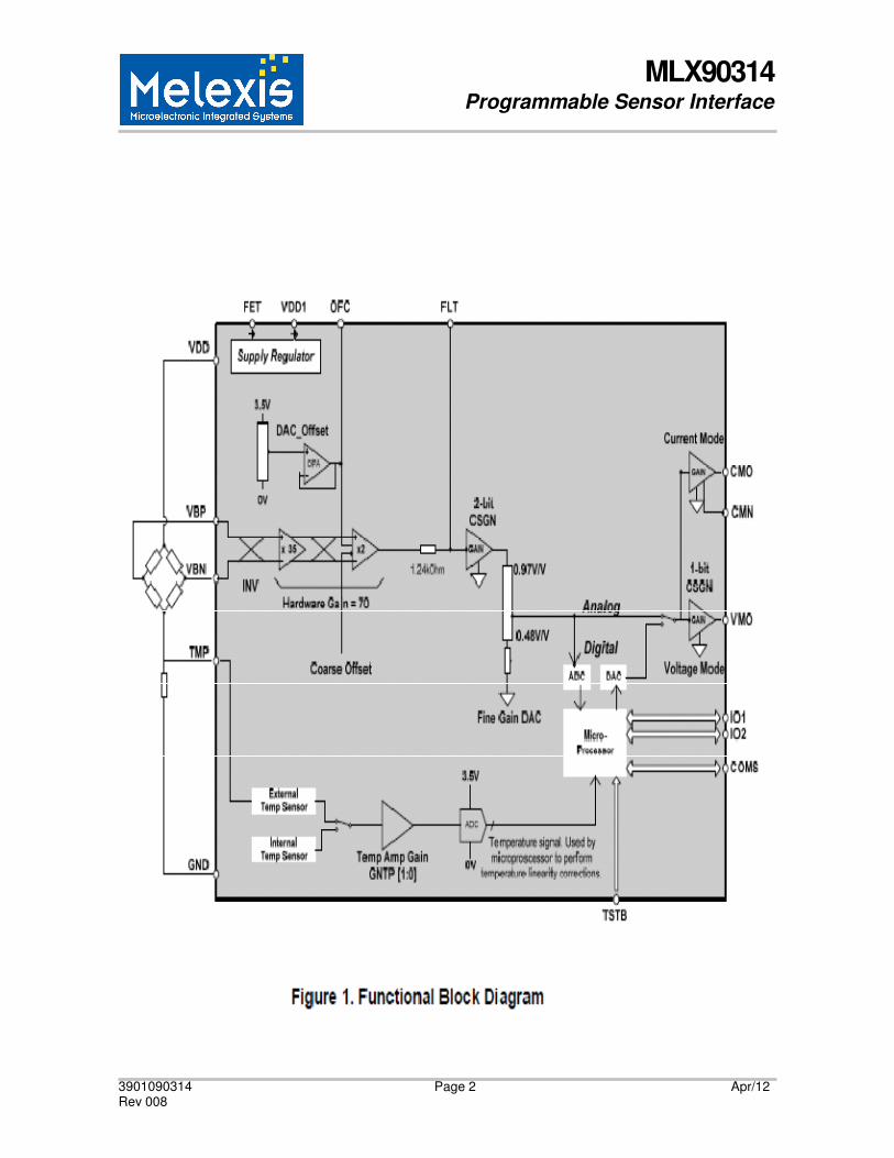
Description The MLX90314 is a dedicated microcontroller which performs signal conditioning for sensors wired in bridge or differential configurations. Sensors that can be used include thermistors, strain gauges, load cells, pressure sensors, accelerometers, etc. The signal conditioning includes gain adjustment, offset control, high order temperature and linearity compensation. Compensation values are stored in EEPROM and are re- programmable. Programming is accomplished by using a PC, with an interface circuit (level shifting and glue logic), and provided software.
The application circuits can provide an output of an absolute voltage, relative voltage, or current. The output can
be range limited with defined outputs when the signal is beyond the programmed limits. Other features include alarm outputs and level steering. The robust electrical design allows the MLX90314 to be used where most signal conditioning and sensor interface circuits cannot be used. Voltage regulation control is provided for absolute voltage and current modes (external FET required).
The standard package is a plastic SO16W. The device is static-sensitive and requires ESD precautions.
MLX90314 Programmable Sensor Interface
3901090314 Rev 008
Page 2 Apr/12
MLX90314 Programmable Sensor Interface
3901090314 Rev 008
Page 3 Apr/12
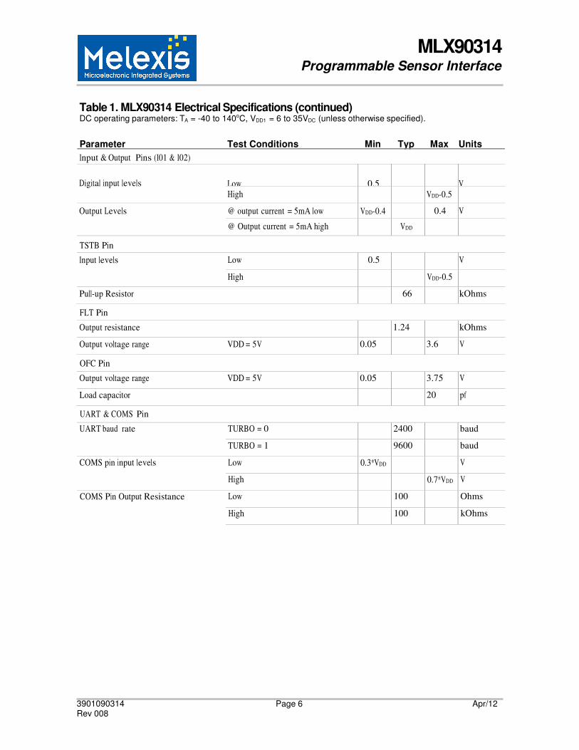
Table 1. MLX90314 Electrical Specifications DC operating parameters: TA = -40 to 140oC, VDD1 = 6 to 35VDC (unless otherwise specified).
Parameter Symbol Test Conditions Min Typ Max Units
Regulator & Consumption
Input voltage range VIN VDD1 (Regulator connected) 6 35 V
Supply current IDD @ TA = 100ºC Current Mode 2.1 mA
Supply current IDD @ TA = 100ºC Voltage Mode 5.0 mA
Regulated supply voltage VREG 4.5 4.75 5.2 V
Regulated voltage
temperature coefficient -600 uV / ºC
Supply rejection ratio PSRR VDD1 > 6V 90 dB
Instrumentation Amplifier
Differential input range VBP-VBN IINV = 0 -2.88 8.38 mV/V(Vdd)
Differential input range VBP-VBN IINV = 1 -8.38 2.88 mV/V(Vdd)
Common mode input range 1/2(VBP+VBN) 38.0 65.0 %VDD
Pin leakage current Pins VBP & VBN to GND, VDD = 8.0 nA
Common mode rejection Ratio CMRR 60 dB
Hardware gain 69 84 V/V
Coarse offset control Range CSOF[1:0] = 00 -4.37 -3.97
mV/V
CSOF[1:0] = 01 -1.46 -1.09 mV/V
CSOF[1:0] = 10 1.09 1.46 mV/V
CSOF[1:0] = 11 3.97 4.37 mV/V
Fixed offset control range High 1.71 2.29 mV/V
Low -2.00 -1.43 mV/V
IA chopper frequency 300 kHz
Gain Stage
Course gain
(Fixed Gain = 1023)
* CSGN = 100 to 111: volta
only, not applicable to curre
Output > 6.5V; MSB = 1
Output < 6.5V; MSB = 0
CSGN = 000 3.0 3.3 V/V
CSGN = 001 4.9 5.4 V/V
ge mode
nt mode.
CSGN = 010 8.0 8.8 V/V
CSGN = 011 12.8 14.1 V/V
CSGN = 100* 7.9 8.7 V/V
CSGN = 101* 12.7 14.0 V/V

MLX90314 Programmable Sensor Interface
3901090314 Rev 008
Page 4 Apr/12
Coarse gain CSGN = 110* 20.4 23.0 V/V
CSGN = 111* 33.1 36.6 V/V
Fixed gain control range 0.480 0.970 V/V
Table 1. MLX90314 Electrical Specifications (continued) DC operating parameters: TA = -40 to 140oC, VDD1 = 6 to 35VDC (unless otherwise specified).
Parameter Test Conditions Min Typ Max Units
Digital Mode & Current Mode Coarse Gain Stage
Course Gain CSGN = 00 1.05 1.17 V/V
CSGN = 01 1.71 1.89 V/V
CSGN = 10 2.77 3.06 V/V
CSGN = 11 4.48 4.95 V/V
Voltage Mode Output Stage ( See Voltage Mode)
Output voltage span CSGN[2:2] = 0 4.5 6.5 V
Gain 2.74 3.04 V/V
CSGN[2:2] = 1 6.5 11 V
Gain 7.24 7.86 V/V
Minimum output voltage -0.2 V
Output source current 2.0 mA
Output sink current @ 0V output voltage 20 uA
Output resistance Over complete output range 25 Ohms
Digital mode output span CSGN[2:2] = 0 6.5 V
CSGN[2:2] = 1 11.0 V
Digital mode step size VDD = 5V, CSGN[2:2]=0 6.5 mV
VDD = 5V, CSGN[2:2]=1 11.0 mV
Capacitive load VMO pin 10 nF
Current Mode Output Stage
Fixed gain RSENSE = 24 ohm 8.4 9.3 mA/V
Output current CMO pin Current mode 27 mA
Current sense resistor 24 Ohms
Digital mode current output span VDD = 5V 23 mA
Digital mode current step Size VDD = 5V,RSENSE=24Ω 30 uA
Signal Path ( General)
Overall gain Voltage mode 98 2100 V/V
Current mode = 24Ω 284 2625 mA/V
Overall non-linearity -0.25 0.25 %
Ratiometry Error (4.75V – 5.25V) Overall Gain < 250V/V -1.75 1.75 %
Overall Gain > 250V/V -4.6 +4.6 %
MLX90314 Programmable Sensor Interface
3901090314 Rev 008
Page 5 Apr/12
Table 1. MLX90314 Electrical Specifications (continued) DC operating parameters: TA = -40 to 140oC, VDD1 = 6 to 35VDC (unless otherwise specified).
Parameter Test Conditions Min Typ Max Units
Bandwidth (-3dB) 39 nF connected from FLT to GND 2.8 3.5 4.2 KHz
Noise, VDD = 5V, CFLT=39nF, CL=10nF, RL =5KΩ, Analog Mode (Max. gain)
Temperature Sensor & - Amplifier
17 mVRMS
Temperature sensor sensitivity 390 uV/ºC
Temperature sensor output voltage 70 380 mV
Temperature Sensor & Amplifier (continued).
Input voltage range TMP pin
@ VDD = 5.0V
GNTP[1,0] = 00 207 517 mV
GNTP[1,0] = 01 145 367 mV
GNTP[1,0] = 10 101 263 mV
GNTP[1,0] = 11 71 186 mV
DAC
Resolution 10 Bit
Monotonicity Guaranteed By Design
Ratiometric output range (DAC output) 1 75 % VDD
Offset Error 10 LSB
Differential non-linearly 1 LSB
Integral non-linearity 2 LSB
ADC
Resolution 10 Bit
Monotonicity Guaranteed by design
Ratiometric input range 1 75 % VDD
Offset error 10 LSB
Differential non-linearly 1 LSB
Integral non-linearity 2 LSB
On-Chip RC Oscillator and Clock
Untrimmed RC oscillator
frequency 40 250 kHz
Trimmed RC oscillator frequency
(Measured at TMP pin with TSTB pin pulled low after power up) 86.9 87.8 88.7 kHz
Frequency temperature coefficiency 26 Hz/ºC
Clock Stability with temperature compensation over full temperature range -3 +3 %
Ratio of f (microcontroller main clock
and (RC oscillator) TURBO = 0 7
TURBO = 1 28
MLX90314 Programmable Sensor Interface
3901090314 Rev 008
Page 6 Apr/12
UART baud rate TURBO = 0 2400 baud
TURBO = 1 9600 baud
COMS pin input levels Low 0.3*VDD V
High 0.7*VDD V
Low 100 Ohms
High 100 kOhms
Table 1. MLX90314 Electrical Specifications (continued) DC operating parameters: TA = -40 to 140oC, VDD1 = 6 to 35VDC (unless otherwise specified).
Parameter Test Conditions Min Typ Max Units
Input & Output Pins (I01 & I02)
Digital input levels
Low
0.5
V
High VDD-0.5
Output Levels @ output current = 5mA low VDD-0.4 0.4 V
@ Output current = 5mA high VDD
TSTB Pin
Input levels Low 0.5 V
High VDD-0.5
Pull-up Resistor 66 kOhms
FLT Pin
Output resistance 1.24 kOhms
Output voltage range VDD = 5V 0.05 3.6 V
OFC Pin
Output voltage range VDD = 5V 0.05 3.75 V
Load capacitor 20 pf
UART & COMS Pin
COMS Pin Output Resistance
MLX90314 Programmable Sensor Interface
3901090314 Rev 008
Page 7 Apr/12
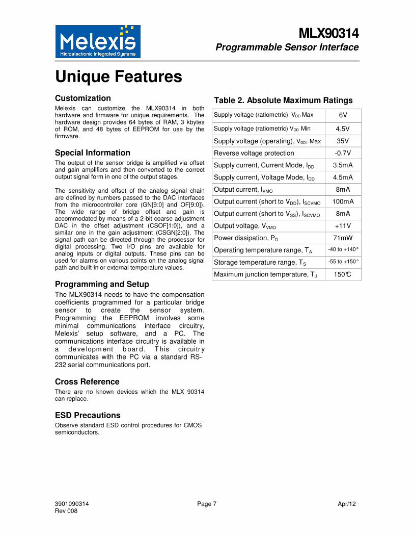
Supply voltage (ratiometric) VDD Max 6V
Supply voltage (ratiometric) VDD Min 4.5V
Supply voltage (operating), VDD1 Max 35V
Reverse voltage protection -0.7V
Supply current, Current Mode, IDD 3.5mA
Supply current, Voltage Mode, IDD 4.5mA
Output current, IVMO 8mA
Output current (short to VDD), ISCVMO 100mA
Output current (short to VSS), ISCVMO 8mA
Output voltage, VVMO +11V
Power dissipation, PD 71mW
Operating temperature range, TA -40 to +140°
Storage temperature range, TS -55 to +150°
Maximum junction temperature, TJ 150°C
Unique Features
Customization Melexis can customize the MLX90314 in both hardware and firmware for unique requirements. The hardware design provides 64 bytes of RAM, 3 kbytes of ROM, and 48 bytes of EEPROM for use by the firmware.
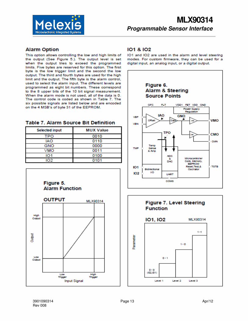
Special Information The output of the sensor bridge is amplified via offset and gain amplifiers and then converted to the correct output signal form in one of the output stages.
The sensitivity and offset of the analog signal chain are defined by numbers passed to the DAC interfaces from the microcontroller core (GN[9:0] and OF[9:0]). The wide range of bridge offset and gain is accommodated by means of a 2-bit coarse adjustment DAC in the offset adjustment (CSOF[1:0]), and a similar one in the gain adjustment (CSGN[2:0]). The signal path can be directed through the processor for digital processing. Two I/O pins are available for analog inputs or digital outputs. These pins can be used for alarms on various points on the analog signal path and built-in or external temperature values.
Programming and Setup
The MLX90314 needs to have the compensation coefficients programmed for a particular bridge sensor to create the sensor system. Programming the EEPROM involves some minimal communications interface circuitry, Melexis’ setup software, and a PC. The communications interface circuitry is available in a de ve lopm ent b oar d. T his circuitr y communicates with the PC via a standard RS- 232 serial communications port.
Cross Reference There are no known devices which the MLX 90314 can replace.
ESD Precautions Observe standard ESD control procedures for CMOS semiconductors.
Table 2. Absolute Maximum Ratings
MLX90314 Programmable Sensor Interface
3901090314 Rev 008
Page 8 Apr/12
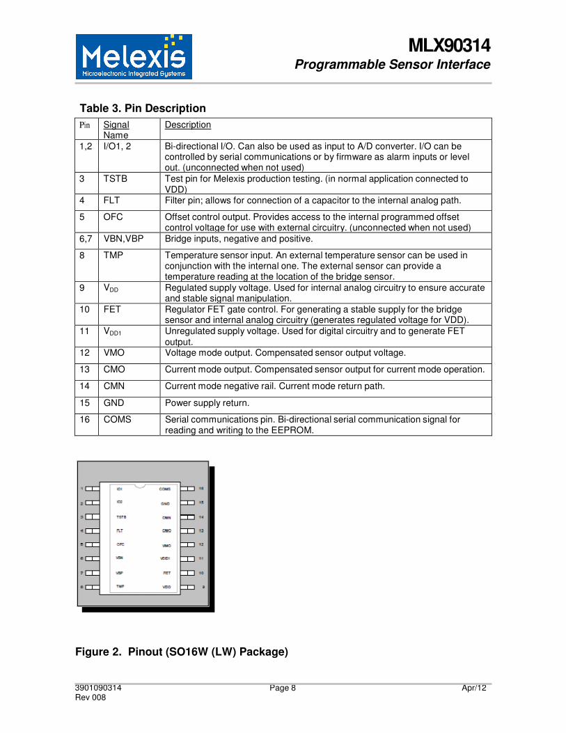
Table 3. Pin Description
Pin Signal Name
Description
1,2 I/O1, 2 Bi-directional I/O. Can also be used as input to A/D converter. I/O can be controlled by serial communications or by firmware as alarm inputs or level out. (unconnected when not used)
3 TSTB Test pin for Melexis production testing. (in normal application connected to VDD)
4 FLT Filter pin; allows for connection of a capacitor to the internal analog path.
5 OFC Offset control output. Provides access to the internal programmed offset control voltage for use with external circuitry. (unconnected when not used)
6,7 VBN,VBP Bridge inputs, negative and positive.
8 TMP Temperature sensor input. An external temperature sensor can be used in conjunction with the internal one. The external sensor can provide a temperature reading at the location of the bridge sensor.
9 VDD Regulated supply voltage. Used for internal analog circuitry to ensure accurate and stable signal manipulation.
10 FET Regulator FET gate control. For generating a stable supply for the bridge sensor and internal analog circuitry (generates regulated voltage for VDD).
11 VDD1 Unregulated supply voltage. Used for digital circuitry and to generate FET output.
12 VMO Voltage mode output. Compensated sensor output voltage.
13 CMO Current mode output. Compensated sensor output for current mode operation.
14 CMN Current mode negative rail. Current mode return path.
15 GND Power supply return.
16 COMS Serial communications pin. Bi-directional serial communication signal for reading and writing to the EEPROM.
Figure 2. Pinout (SO16W (LW) Package)
MLX90314 Programmable Sensor Interface
3901090314 Rev 008
Page 9 Apr/12
Analog Features
Supply Regulator A bandgap-stabilized supply-regulator is on-chip while the pass-transistor is external. The bridge-type sensor is typically powered by the regulated supply (typically 4.75V). For ratiometric operation, the supply-regulator can be disabled by connecting together the unregulated and regulated supply pins.
Oscillator The MLX90314 contains a programmable on-chip RC oscillator. No external components are needed to set the frequency (87.8 kHz +/-1%). The MCU-clock is generated by a PLL (phase locked loop tuned for 614 kHz or 2.46 Mhz) which locks on the basic oscillator.
The frequency of the internal clock is stabilized over the full temperature range, which is divided into three regions, each region having a separate digital clock setting. All of the clock frequency programming is done by Melexis during final test of the component. The device uses the internal temperature sensor to determine which temperature range setting to use.
A/D and D/A
Power-On Reset The Power-On Reset (POR) initializes the state of the digital part after power up. The reset circuitry is completely internal. The chip is completely reset and fully operational 3.5 ms from the time the supply crosses 3.5 volts. The POR circuitry will issue another POR if the supply voltage goes below this threshold for 1.0 us.
Test Mode For 100% testability, a "TEST" pin is provided. If the pin is pulled low, then the monitor program is entered and the chip changes its functionality. In all other applications, this pin should be pulled high or left floating (internal pull-up).
Temperature Sense The temperature measurement, TPO, is generated from the external or internal temperature sensor. This is converted to a 10-bit number for use in calculating the signal compensation factors. A 2-bit coarse adjustment GNTP[1:0] is used for the temperature signal gain & offset adjustment.
Conversions using only one DAC For saving chip area, the "Offset DAC" is multiplexed in various ways. Both "fine offset" and "digital mode" signals are stored on a capacitor. An ADC-loop is available by using a comparator and SAR.
D/A Before changing to another capacitor, the DAC output should be settled to the new value. For example, MODSEL moves the analog multiplexer to the so- called "open state 0." At the same time, the 10 bit mux selects OF[9:0] for the offset-DAC. After the DAC settling time, the analog multiplexer is moved to its final state and the DAC-output is stored on a capacitor.
A/D The S/W-Signal MODSEL connects the SAR-output to the DAC and the DAC-output to the comparator. The SARegister is initialized by a rising edge of STC (S/W signal). At the end of the A/D conversion, the EOC flag is set to 1 and the controller can read the ADC values.
3901090314 Rev 008
Page 10 Apr/12
MLX90314 Programmable Sensor Interface
Digital Features
Microprocessor, LX11 Core, Interrupt Controller, Memories The LX11 microcontroller core is described in its own datasheet. As an overview, this implementation of the LX11 RISC core has following resources:
Two accumulators, one index and two interrupt accumulators.
15 - 8 bit I/O ports to internal resources. 64 byte RAM. 4 kbytes ROM : 3 kbytes is available for the
customer's application firmware. 1k is reserved for test.
48 x 8 bit EEPROM. Four interrupt sources, two UART interrupts and two timers.
UART The serial link is a potentially full-duplex UART. It is receive-buffered, in that it can receive a second byte before a previously received byte has been read from the receiving register. However, if the first byte is not read by the time the reception of the second byte is completed, the first byte will be lost. The UART's baud rate depends on the RC-oscillator's frequency and the "TURBO"-bit (see output port). Transmitted and received data has the following structure: start bit = 0, 8 bits of data, stop bit = 1.
Sending Data Writing a byte to port 1 automatically starts a transmission sequence. The TX Interrupt is set when the STOP-bit of the byte is latched on the serial line.
Receiving Data Reception is initialized by a 1 to 0 transition on the serial line (i.e., a START-bit). The baud rate period (i.e., the duration of one bit) is divided into 16 phases. The first six and last seven phases of a bit are not used. The decision on the bit-value is then the result of a majority vote of phase 7, 8 and 9 (i.e., the center of the bit).
Spike synchronization is avoided by de-bouncing on the incoming data and a verification of the START-bit value. The RX Interrupt is set when the stop bit is latched in the UART.
Timer The clock of the timers TMI and TPI is taken directly from the main oscillator. The timers are never reloaded, so the next interrupt will take place 2x oscillator pulses after the first interrupt.
Watch Dog An internal watch dog will reset the whole circuit in case of a software crash. If the watch dog counter is not reset at least once every 26 milliseconds (@ 2.46 MHz main clock), the microcontroller and all the peripherals will be reset.
Firmware The MLX90314 firmware performs the signal conditioning by either of two means: analog or digital. The analog signal conditioning allows separate offset and gain temperature coefficients for up to four temperature ranges. Digital mode allows for all of the analog capabilities plus up to five different gain values based on the input signal level. Also available in both modes is the capability of range limiting and level steering.
Temperature Processing In both analog and digital modes, the temperature reading controls the temperature compensation. This temperature reading is filtered as designated by the user. The filter adjusts the temperature reading by factoring in a portion of the previous value. This helps to minimize the effect of noise when using an external temperature sensor. The filter equation is: If measured_temp > Temp_f(n) then Temp_f(n+1) = Temp_f(n) + [measured_temp -
Temp_f(n)] / [2 n_factor]. If measured_temp < Temp_f(n), then Temp_f(n+1) = Temp_f(n) - [measured_temp -
Temp_f(n)] [2 n_factor].
Temp_f(n+1) = new filtered temperature value. Temp_f(n) = previous filtered temperature value. Measured_temp = Value from temperature A to D. N_factor = Filter value set by the user (four
LSB’s of byte 25 of EEPROM), range 0-6.
The filtered temperature value, Temp_f, is stored in RAM bytes 58 and 59. The data is a 10 bit value, left justified in a 16 bit field.

3901090314 Rev 008
Page 11 Apr/12
MLX90314 Programmable Sensor Interface
Different Modes
Analog Mode The parameters OF and GN represent, respectively, offset correction and span control, while OFTCi and GNTCi represent their temperature coefficients (thermal zero shift and thermal span shift). After reset, the firmware continuously calculates the offset and gain DAC settings as follows: The EEPROM holds parameters GN, OF, OFTCi and GNTCi, where “i” is the gap number and can be 1 < i < 4. The transfer
OFFSET DAC_OFFSET (new value) ~ OF[9:0]+[OFTCi* dT] OF[9:0] = Fixed Gain, bytes 4 and 17 in EEPROM. OFTCi = Offset for a given temperature
segment I. OFTCiL and OFTCiH in EEPROM table.
dT = Temp. change within the appropriate gap. Calculation of the offset for a given temperature seg- ment is performed the same way as for the gain.
[mV/V]
function is described below.
Vout = FG * DAC_GAIN * CSGN[2:0] * Vin+DAC_OFFSET+CSOF
Iout = FG * DAC_GAIN * CSGN[1:0] * Vin+DAC_OFFSET+CSOF * 8.85mA/V
FG = Hardware Gain (~72V/V). Part of the hardware
design, and not changeable. CSGN = Course Gain, part of byte 2 in EEPROM. CSOF = Coarse Offset, part of byte 2 in EEPROM.
GAIN DAC_GAIN (new value) ~ GN[9:0] + [GNTCi * dT]
GN[9:0] = Fixed Gain, bytes 3 and 17 in EEPROM. GNTCi = Gain TC for a given temperature
segment I. GNTCiL and GNTCiH in EEPROM table.
dT = Temp. change within the appropriate gap.
How to calculate gain in the first temp. gap?:
DAC_GAIN = GN[9:0] - GNTC1 * (T1 – Temp_f1)
How to calculate gain in the other temp. gaps?:
2nd gap: DAC_GAIN = GN[9:0] + GNTC2 * (Temp_f2 – T1)
3th gap: DAC_GAIN = DAC_GAIN2 + GNTC3 * (Temp_f3 – T2)
4th gap: DAC_GAIN = DAC_GAIN3 + GNTC4 * (Temp_f4 – T3)
Where: Temp_f = Filtered temp. (previously described).
If GNTC1 > 2047 => DAC_GAIN
If GNTC2,3,4 > 2047 => DAC_GAIN
Digital Mode
The MLX90314 firmware provides the capability of digitally processing the sensor signal in addition to the analog processing. This capability allows for signal correction.
Signal Correction While in digital mode the firmware can perform signal correction. This is an adjustment to the output level based on the input signal level. Adjustment coefficients can be set for five different signal ranges. The output is obtained by the following formula:
Output = (Signal – Pi) * Pci + Poff where Signal = input signal measurement; Poff = Pressure ordinate Pi = Pressure signal point (I = 2,3,4,5) Pci = programmed coefficient.
The PCi coefficients are coded on 12 bits: one bit for the sign, one for the unity, and the rest for the decimals. The Pi are coded on 10 bits (0-3FFh) in high-low order. PNB_TNB: contains the number of signal points, coded on the four MSB’s. The four LSB’s are reserved for the number of temperature points. See Table 4 and Table 5.
Compensation Trade-Offs A compromise must be made between temperature compensation and pressure correction. The EEPROM space where the signal coefficients are stored is shared with the temperature coefficients, with the result that an EEPROM byte can be used either for a temperature coefficient or for a signal coefficient, but not both. Table 6 presents the possibilities among the maximum number of temperature gaps and the maximum number of signal gaps

3901090314 Rev 008
Table 4. PNB_TNB Bit DPressure Gaps
# of Pressure Gaps 4MSB of PNB
Fixed 15 (F
1 14 (E
2 12 (C
3 10 (A
4
5
Table 5. PNB_TNB Bit DTemperature Gap
# of Temperature Gaps
4 LSB
Fixed (1)
2 Gaps
3 Gaps
4 Gaps 11 (B
Page 12
MLXProgrammable Sensor
Maximum number of
temperature gaps Maximu
s
Fixed Gain and
fixed Offset
2 Gaps
3 Gaps
4 Gaps
F
Outp
ut (u
nits)
Definition; s
PNB_TNB Value 5 (F hex)
4 (E hex)
2 (C hex)
0 (A hex)
8
6
Definition; ps
Table 6. Tempera& Signal Limitatio
of PNB_TNB
0
5
8
1 (B hex)
Figure 4. Signa
Linearity Correc
Output
PC4
ML
PC5
PC3
PC2
PC1
0 P2 P3 P4 P5
Apr/12
MLX90314 r Interface
mum number of
signal gaps
5 Gaps
3 Gaps
2 Gaps
Fixed signal
ature ons
gnal
ction
LX90314
C5
3901090314 Rev 008
Page 13 Apr/12
MLX90314 Programmable Sensor Interface

3901090314 Rev 008
Page 14 Apr/12
MLX90314 Programmable Sensor Interface
Selected input MUX Value TPO 0010 IAO 0110
GNO 0000 VMO 0011
Bit
Function
Remarks
7 1= EEPROM Checksum test active 0= EEPROM Checksum test inactive
EEPROM Checksum test. Checksum test failure will force the output to the value programmed in bytes 40 and 41 of the EEPROM (See Table 10).
6 0 = Analog Mode 1 = Digital Mode
Digital mode must be activated when VMO and CMO both active.
5 0 = Alarm function inactive 1 = Alarm function active
Alarm functions are like “limiting functions”: If defined ADC INPUT is below low alarm trigger,
then DIGMOD becomes active with alarm low output).
If defined ADC INPUT is above high alarm trigger, then DIGMOD becomes active with alarm high output.
Note: Deactivated if the level steering mode is active
4 0 = IO1/IO2 are not active outputs 1 = level steering: IO1/IO2 are active outputs
Depending on the sampled input, IO1/IO2 will be a two bit digital output. If IO1/IO2 are not active outputs, then they will be analog inputs.
3 0 = Turbo inactive 1 = Turbo active
2 0 = VMO inactive 1 = VMO active
1 0 = Internal temperature sensor active 1 = External temperature sensor active
0 0 = CMO inactive 1 = CMO active
CMO has fixed digital value (EEPROM byte - see below) if both VMO and CMO are active. To activate this value, the digital mode must be activated.
Level Steering The level steering option allows configuration of the IO pins as outputs to indicate the relative level of a selected signal. See Figure 7. The levels at which the two outputs change state are programmed by the user. The programmed levels are set as eight bit numbers and compared to the upper eight bits of the digitized signal. This function utilizes the same resources as the alarm function. The two functions (level steering and alarm) can not be used simultaneously. Four bytes in the EEPROM command this option. The first byte is used to select the input, while the last three comprise the transition levels. The control byte for the level steering is the same as for the alarm. The four MSB’s hold the code for the selected input. The control byte has several possibilities as designated by the MUX settings (See Table 8)
Communications The MLX90314 firmware transfers a complete byte of data into and from the memory based on a simple command structure. The commands allow data to be read and written to and from the EEPROM and read from the RAM. RAM data that can be read includes the current digitized temperature and digitized GNO. The commands are described below. Melexis provides setup software for programming the MLX90314.
Table 8. Level Steering Bit Definitions
Table 9. Mode Byte Bit Definition

3901090314 Rev 008
Page 15 Apr/12
MLX90314 Programmable Sensor Interface
UART Commands The commands can be divided into three parts: (1) downloading of data from the ASIC, (2) uploading of data to the ASIC and (3) the reset command. All the commands have the same identification bits. The two MSB’s of the sent byte indicate the command while the last six MSB’s designate the desired address. The commands are coded as followed: 11 to read a RAM byte. 10 to read an EEPROM byte. 01 to write in the EEPROM. 00 to write in the RAM.
The addresses can include 0-63 for the RAM, 0-47 for the EEPROM, and 63 for the EEPROM, RESET Command (read).
Downloading Command With one byte, data can be downloaded from the ASIC. The ASIC will automatically send the value of the desired byte.
Uploading Command Writing to the RAM or EEPROM involves a simple handshaking protocol in which each byte transmitted is acknowledged by the firmware. The first byte transmitted to the firmware includes both command and address. The firmware acknowledges receipt of the command and address byte by echoing the same information back to the transmitter. This “echo” also indicates that the firmware is ready to receive the byte of data to be stored in RAM or EEPROM. Next, the byte of value to be stored is transmitted and, if successfully received and stored by the firmware, is acknowledged by a “data received signal,” which is two bytes of value BCh. If the “data received signal” is not observed, it may be assumed that no value has been stored in RAM or EEPROM.
Reset Command Reading the address 63 of the EEPROM resets the ASIC and generates a received receipt indication. Immediately before reset, the ASIC sends a value of BCh to the UART, indicating that the reset has been received.
EEPROM Data All user-settable variables are stored in the EEPROM within the MLX90314. The EEPROM is always re- programmable. Changes to data in the EEPROM do not take effect until the device is reset via a soft reset or power cycle. 12 bit variables are stored on 1.5 bytes. The 4 MSB’s are stored in a separate byte and shared with the four MSB’s of another 12-bit variable.
Clock Temperature Stabilization To provide a stable clock frequency from the internal clock over the entire operating temperature range, three separate clock adjust values are used. Shifts in operating frequency over temperature do not effect the performance but do, however, cause the communications baud rate to change. The firmware monitors the internal temperature sensor to determine which of three temperature ranges the device currently is in. Each temperature range has a factory set clock adjust value, ClkTC1, ClkTC2, and ClkTC3. The temperature ranges are also factory set. The Ctemp1 and Ctemp2 values differentiate the three ranges. In order for the temperature A to D value to be scaled consistently with what was used during factory programming, the CLKgntp (temperature amplifier gain) valued is stored. The Cadj value stored in byte 1 of the EEPROM is used to control the internal clock frequency while the chip boots.
Unused Bytes There are eight unused bytes in the EEPROM address map. These bytes can be used by the user to store information such as a serial number, assembly date code, production line, etc. Melexis doesn’t guarantee that these bytes will be available to the user in future revisions of the firmware.
EEPROM Checksum A checksum test is used to ensure the contents of the EEPROM. The eight bit sum of all of the EEPROM addresses should have a remainder of 0FFh when the checksum test is enabled (mode byte). Byte 47 is used to make the sum remainder totals 0FFh. If the checksum test fails, the output will be driven to a user defined value, Faultval. When the checksum test is enabled, the checksum is verified at initialization of RAM after a reset.
RAM Data All the coefficients (pressure, temperature) are compacted in a manner similar to that used for the EEPROM. They are stored on 12 bits (instead of keeping 16 bits for each coefficient). All the measurements are stored on 16 bits. The user must have access to the RAM and the EEPROM, while interrupt reading of the serial port. Therefore, bytes must be kept available for the return address, the A- accu and the B-accu, when an interrupt occurs. The RAM keeps the same structure in the both modes.

3901090314 Rev 008
Page 16 Apr/12
MLX90314 Programmable Sensor Interface
Decimal
Value
Hexadecimal
Equivalent
Fixed Point Signed
Number Equivalent
0 0000h +0.00
1023 3FFh +0.9990234
1024 400h +1.000
2047 7FFh +1.9990234
2048 800h -0.000
3071 0BFFh -0.9990234
3072 0C00h -1.000
4095 0FFFh -1.9990234
Table 10. Examples of Fixed Point Signed Numbers
Data Range Various data are arranged as follows:
Temperature points: 10 bits, 0-03FF in high- low order.
Pressure points: 10 bits, 0-03FF in high-low order.
GN1: 10 bits, 0-03FF in high-low order.
OF1: 10 bits, 0-03FF in high-low order.
GNTCi: signed 12 bits (with MSB for the sign), [-1.9990234, +1.9990234].
OFTCi: signed 12 bits (with MSB for the sign), [-1.9990234, +1.9990234].
Pci: signed 12 bits (with MSB for the sign), [-1.9990234, +1.9990234] DIGMO: 10 bits, 0-03FF in high-low order (See Table 13 for examples of fixed point signed numbers.)
Table 11. EEPROM Byte Definitions
Byte
Designation
Note
0 MODE byte Contents described in Table 9.
1 Cadj Controls system clock during boot.
2 Coarse Control Contents described in Table 12.
3 GN1L The eight LSB's of the Fixed Gain, GN[7:0].
4 OF1L The eight LSB's of Fixed Offset OF[7:0].
5 GNTC1L The eight LSB's of the first gain TC GNTC1[7:0].
6 OFTC1L The eight LSB's of the first offset TC OFTC1[7:0].
7 TR1L PC5L
The eight LSB's of the first temperature point, T1[7:0]. The eight LSB's of Pressure Coefficient 5 PC5[7:0].
8 GNTC2L P5L
The eight LSB's of the second gain TC GNTC2[7:0]. The eight LSB's of Pressure Point 5 P5[7:0].
9 OFTC2L PC4L
The eight LSB's of the second offset TC OFTC2[7:0]. The eight LSB's of Pressure Coefficient 4 PC4[7:0].
10 TR2L P4L
The eight LSB's of the second temperature point T2[7:0]. The eight LSB's of Pressure Point 4 (or Signature) P4[7:0].
11 GNTC3L PC3L
The eight LSB's of the third gain TC GNTC3[7:0]. The eight LSB's of Pressure Coefficient 3 (or Signature) PC3 [8:0].
3901090314 Rev 008
Page 17 Apr/12
MLX90314 Programmable Sensor Interface
Table 11. EEPROM Byte Definitions (continued)
Byte
Designation
Note
12 OFTC3L or
P3L
The eight LSB's of the third offset TC OFTC3[7:0]. The eight LSB's of Pressure Point 2 (or Signature) P2[7:0].
13 TR3L or
PC2L The eight LSB's of the third temperature point T3[7:0]. The eight LSB's of Pressure Coefficient 2 PC2[7:0].
14 GNTC4L or
P2L The eight LSB's of the fourth gain TC GNTC4[7:0]. The eight LSB's of Pressure Point 2 P2[7:0].
15 OFTC4L or
PC1L The eight LSB's of the fourth offset TC OFTC4. The eight LSB's of Pressure Coefficient 1 PC1
16 PoffL The eight LSB's of Pressure (output signal) Ordinate Poff[7:0].
Upper Lower
Four Four
Bits Bits
Upper four bits. Lower four bits
17 GN1[9:8] OF1[9:8] Two MSB's of fixed gain Two MSB's of fixed offset GN[9:8]. OF[9:8]
18 GNTC1[11:8] OFTC1[11:8] Four MSB's of first gain TC Four MSB's of the first offset GNTC1[11:8]. TC OFTC1[11:8].
19 TR1[9:8] GNTC2[11:8]
PC5[11:8] P5[9:8]
Two MSB's, first temperature Four MSB's, second gain point T1[9:8] or TC GNTC2[11:8] or Four MSB's, Pressure TC GNTC2[11:8] or Coefficient 5 PC5[11:8]. Two MSB's Pressure Point 5
P5[9:8].
20 OFTC2[11:8] TR2[9:8]
PC4[11:8] P4[9:8]
Four MSB's second offset Two MSB's second TC OFTC2[11:8] or temperature point T2[9:8] or Four MSB's Pressure Two MSB's Pressure Point 4 Coefficient 4 PC4[11:8]. P4[9:8].
21 GNTC3[11:8] OFTC3[11:8]
PC3[11:8] P3[9:8]
Four MSB's third gain TC Four MSB's third offset GNTC3[11:8] or TC OFTC3[11:8] or Four MSB's Pressure Two MSB's Pressure Point 3 Coefficient 3 PC3[11:8]). P3[9:8].
22 TR3[9:8] GNTC4[11:8]
PC2[9:8] P2[9:8]
Two MSB's third Four MSB's fourth gain TC temperature point t3[9:8] or GNTC4[11:8] or Four MSB's Pressure Two MSB's Pressure Coefficient 2 PC2[11:8]. Point 2 P2[9:8].
23 OFTC4[11:8] Poff[9:8]
PC1[11:8]
Four MSB's fourth offset TC Two MSB's Pressure ordinate OFTC4[11:8] or Poff[9:8]. Four MSB's Pressure Coefficient 1 PC1[11:8].
3901090314 Rev 008
Page 18 Apr/12
MLX90314 Programmable Sensor Interface
Table 11. EEPROM Byte Definitions (continued)
Byte
Designation
Note
24 PNB_TNB Number of temperature and pressure gaps. See Tables 4, 5, and 6, and Figures 3 and 4.
25 n_factor Temperature filter coefficient, four LSB's. Four MSB's must all be zero.
26 Not used This byte is not used.
27 ALARM low trigger Level1 IO2/IO1
Value below which ALARM will go on. Value of first level ([IO2, IO1]= 00-01). See Figures 5 & 7.
28 ALARM low output Level2 IO2/IO1
Value of DIGMO during “ALARM low” condition. Value of second level ([IO2,IO1] = 01-10). See Figures 5 and 7
29 ALARM high trigger Level3 IO2/IO1
Value above which ALARM will go on. Value of third level ([IO2,IO1]=10-11). See Figures 5 and 7.
30 ALARM high out level Value of DIGMO during “ALARM high” condition. See Figures 5 and 7.
31 ALARM control byte
IO1/IO2 control byte
Four LSB's are unused
Three bits needed for choice of input for ALARM detection (TPO, IAO, GNO, VMO, IO1 or IO2). Two bits needed for choice of input for LEVEL-steering (TPO, IAO, GNO or VMO). The above bits are multiplexed according to the mode. If both CMO and VMO are active, then alarm is not active.
32 ClkTC1 Value of Cadj at low temperature (Don’t change; factory set).
33 ClkTC2 Value of Cadj at mid temperature (Don’t change; factory set).
34 ClkTC3 Value of Cadj at high temperature Don’t change; factory set).
35 Ctemp1 First Cadj temperature point, eight MSB’s of the 10 bit internal temperature value (set at factory; do not change).
36 Ctemp2 Second Cadj temperature point, eight MSB’s of the 10 bit internal temperature value (set at factory; do not change).
37-38 Not used These bytes are not used by the firmware and are available to the user.
39 CLKgntp Setting for temperature amplifier for clock temperature adjustment temperature reading (set at factory; do not change).
40-41 Faultval Value sent to output if checksum test fails is a 10 bit value.
42-46 Not Used These bytes are not used by the firmware and are available to the user.
47 Checksum EEPROM checksum; value needed to make all bytes add to 0FFh. Must be set by user if checksum test is active.

3901090314 Rev 008
Page 19 Apr/12
MLX90314 Programmable Sensor Interface
Bit Symbol Function
7 IINV Invert signal sign.
6 GNTP1 Gain & offset of temperature amplifier.
GNTP = 0 to 3. 5 GNTP0
4 CSOF 1 Coarse offset of signal amplifier.
CSOF = 0 to 3. 3 CSOF 0
2 CSGN2 Coarse gain of signal amplifier. CSGN = 0 to 7. If CSGN > 3, output range = 0 to 10V. If CSGN <= 3, output range = 0 to 5V.
1 CSGN1
0 CSGN0
Notes For Table 11 1. Not all the temperature and pressure coefficients must be used. When a coefficient is unused, the eight LSB’s and the four MSB’s are replaced by 0.
2. The level steering and the alarm mode cannot be active simultaneously because the levels bytes are shared with the two modes.
3. If the alarm mode and the level steering are both active, the level steering mode is dominant. The firmware will run with the level steering mode, by default.
4. If the DIGMO mode (VMO and CMO both active) is active, the alarm will be automatically disabled by the firmware.
5. At PNB_TNB address, the four MSB's correspond to the address of the last pressure point and the four LSB’s to the address of the last temperature point.
6. In the alarm_control variable, the selected input is stored on the three MSB’s.
7. Pi and OFi are 10 bit values, right justified in 12 bits fields.
Table 12. Bit Definitions; Coarse Control , Byte 2
Table 13. RAM Byte Definitions
Byte
Functions
Remarks
0 MODE byte See Table 9.
1 GN1L Fixed gain number (8LSB).
2 OF1L Fixed offset number (8LSB).
3 GNTC1L First gain TC (8LSB).
4 OFTC1L First offset TC (8LSB).
5 TR1L PC5L
First temperature point. Pressure Coefficient 5 (8LSB).
6 GNTC2L P5L
Second gain TC. Pressure point 5 (8LSB).
7 OFTC2L PC4L
Second offset TC. Pressure coefficient 4 (8LSB).
8 TR2L P4L
Second temperature point. Pressure Point 4 (or Signature) (8LSB).
9 GNTC3L PC3L
Third gain TC. Pressure Coefficient 3 (or Signature) (8LSB).
10 OFTC3L P3L
Third offset TC. Pressure Point 2 (or Signature) (8LSB).
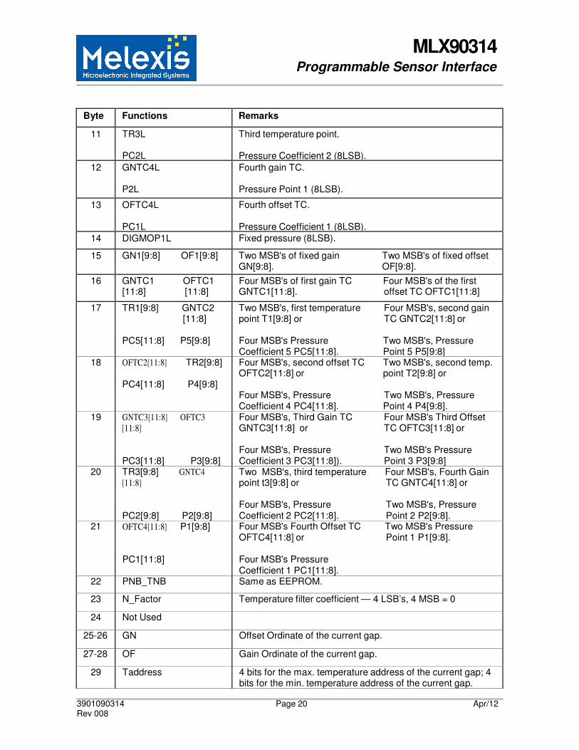
MLX90314 Programmable Sensor Interface
3901090314 Rev 008
Page 20 Apr/12
Byte Functions Remarks
11 TR3L
PC2L
Third temperature point.
Pressure Coefficient 2 (8LSB). 12 GNTC4L
P2L
Fourth gain TC.
Pressure Point 1 (8LSB).
13 OFTC4L
PC1L
Fourth offset TC.
Pressure Coefficient 1 (8LSB). 14 DIGMOP1L Fixed pressure (8LSB).
15 GN1[9:8] OF1[9:8] Two MSB's of fixed gain Two MSB's of fixed offset GN[9:8]. OF[9:8].
16 GNTC1 OFTC1 [11:8] [11:8]
Four MSB's of first gain TC Four MSB's of the first GNTC1[11:8]. offset TC OFTC1[11:8]
17 TR1[9:8] GNTC2 [11:8]
PC5[11:8] P5[9:8]
Two MSB's, first temperature Four MSB's, second gain point T1[9:8] or TC GNTC2[11:8] or
Four MSB's Pressure Two MSB's, Pressure Coefficient 5 PC5[11:8]. Point 5 P5[9:8]
18 OFTC2[11:8] TR2[9:8]
PC4[11:8] P4[9:8]
Four MSB's, second offset TC Two MSB's, second temp. OFTC2[11:8] or point T2[9:8] or
Four MSB's, Pressure Two MSB's, Pressure Coefficient 4 PC4[11:8]. Point 4 P4[9:8].
19 GNTC3[11:8] OFTC3
[11:8]
PC3[11:8] P3[9:8]
Four MSB's, Third Gain TC Four MSB's Third Offset GNTC3[11:8] or TC OFTC3[11:8] or
Four MSB's, Pressure Two MSB's Pressure Coefficient 3 PC3[11:8]). Point 3 P3[9:8]
20 TR3[9:8] GNTC4
[11:8]
PC2[9:8] P2[9:8]
Two MSB's, third temperature Four MSB's, Fourth Gain point t3[9:8] or TC GNTC4[11:8] or
Four MSB's, Pressure Two MSB's, Pressure Coefficient 2 PC2[11:8]. Point 2 P2[9:8].
21 OFTC4[11:8] P1[9:8]
PC1[11:8]
Four MSB's Fourth Offset TC Two MSB's Pressure OFTC4[11:8] or Point 1 P1[9:8].
Four MSB's Pressure Coefficient 1 PC1[11:8].
22 PNB_TNB Same as EEPROM.
23 N_Factor Temperature filter coefficient — 4 LSB’s, 4 MSB = 0
24 Not Used
25-26 GN Offset Ordinate of the current gap.
27-28 OF Gain Ordinate of the current gap.
29 Taddress 4 bits for the max. temperature address of the current gap; 4 bits for the min. temperature address of the current gap.
MLX90314 Programmable Sensor Interface
3901090314 Rev 008
Page 21 Apr/12
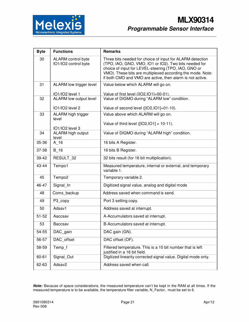
Byte Functions Remarks
30 ALARM control byte IO1/IO2 control byte
Three bits needed for choice of input for ALARM detection (TPO, IAO, GNO, VMO, IO1 or IO2). Two bits needed for choice of input for LEVEL-steering (TPO, IAO, GNO or VMO). These bits are multiplexed according the mode. Note: if both CMO and VMO are active, then alarm is not active.
31 ALARM low trigger level
IO1/IO2 level 1
Value below which ALARM will go on.
Value of first level ([IO2,IO1]=00-01). 32 ALARM low output level
IO1/IO2 level 2
Value of DIGMO during “ALARM low” condition.
Value of second level ([IO2,IO1]=01-10).
33 ALARM high trigger level
IO1/IO2 level 3
Value above which ALARM will go on.
Value of third level ([IO2,IO1] = 10-11).
34 ALARM high output level
Value of DIGMO during “ALARM high” condition.
35-36 A_16 16 bits A Register.
37-38 B_16 16 bits B Register.
39-42 RESULT_32 32 bits result (for 16 bit multiplication).
43-44 Tempo1 Measured temperature, internal or external, and temporary variable 1.
45 Tempo2 Temporary variable 2.
46-47 Signal_In Digitized signal value, analog and digital mode
48 Coms_backup Address saved when command is send.
49 P3_copy Port 3 setting copy.
50 Adsav1 Address saved at interrupt.
51-52 Aaccsav A-Accumulators saved at interrupt.
53 Baccsav B-Accumulators saved at interrupt.
54-55 DAC_gain DAC gain (GN).
56-57 DAC_offset DAC offset (OF).
58-59 Temp_f Filtered temperature. This is a 10 bit number that is left justified in a 16 bit field.
60-61 Signal_Out Digitized linearity corrected signal value. Digital mode only.
62-63 Adsav2 Address saved when call.
Note: Because of space considerations, the measured temperature can’t be kept in the RAM at all times. If the measured temperature is to be available, the temperature filter variable, N_Factor, must be set to 6.
MLX90314 Programmable Sensor Interface
3901090314 Rev 008
Page 22 Apr/12
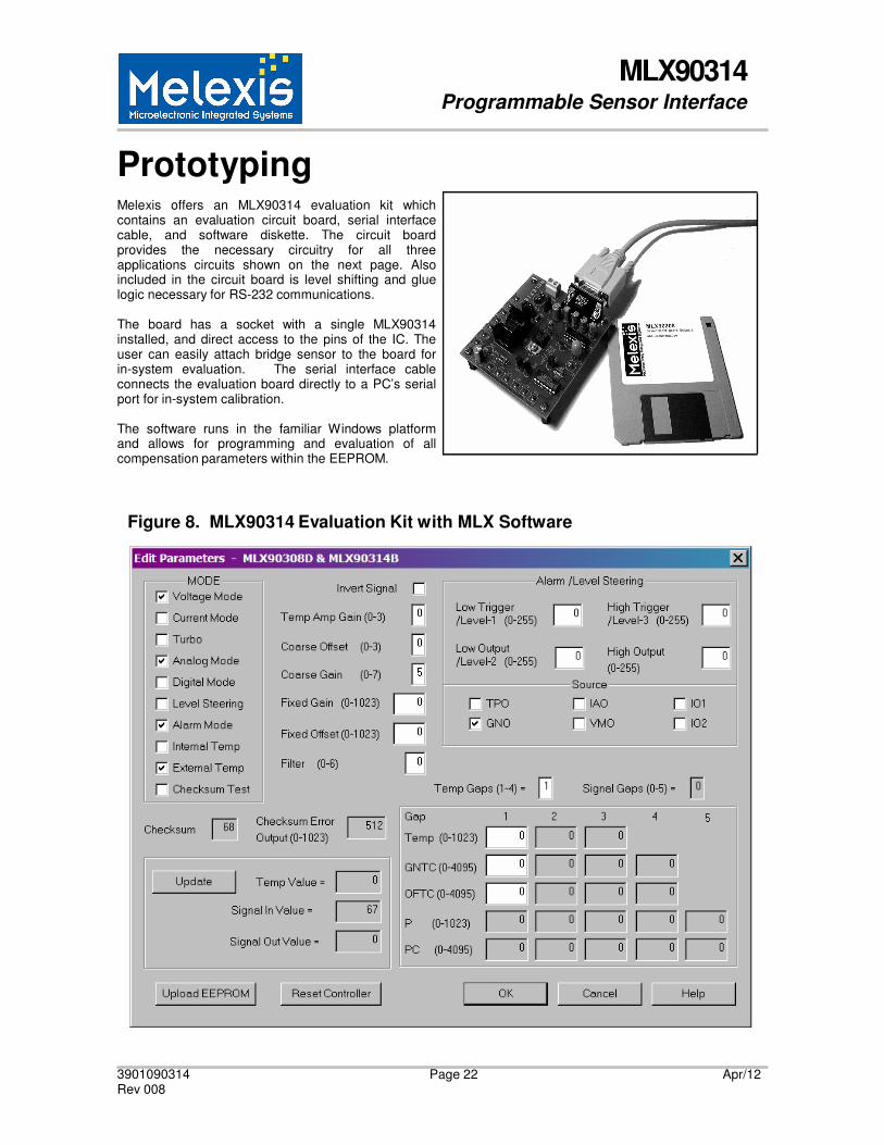
Prototyping
Melexis offers an MLX90314 evaluation kit which contains an evaluation circuit board, serial interface cable, and software diskette. The circuit board provides the necessary circuitry for all three applications circuits shown on the next page. Also included in the circuit board is level shifting and glue logic necessary for RS-232 communications.
The board has a socket with a single MLX90314 installed, and direct access to the pins of the IC. The user can easily attach bridge sensor to the board for in-system evaluation. The serial interface cable connects the evaluation board directly to a PC’s serial port for in-system calibration.
The software runs in the familiar Windows platform and allows for programming and evaluation of all compensation parameters within the EEPROM.
Figure 8. MLX90314 Evaluation Kit with MLX Software
MLX90314 Programmable Sensor Interface
3901090314 Rev 008
Page 23 Apr/12
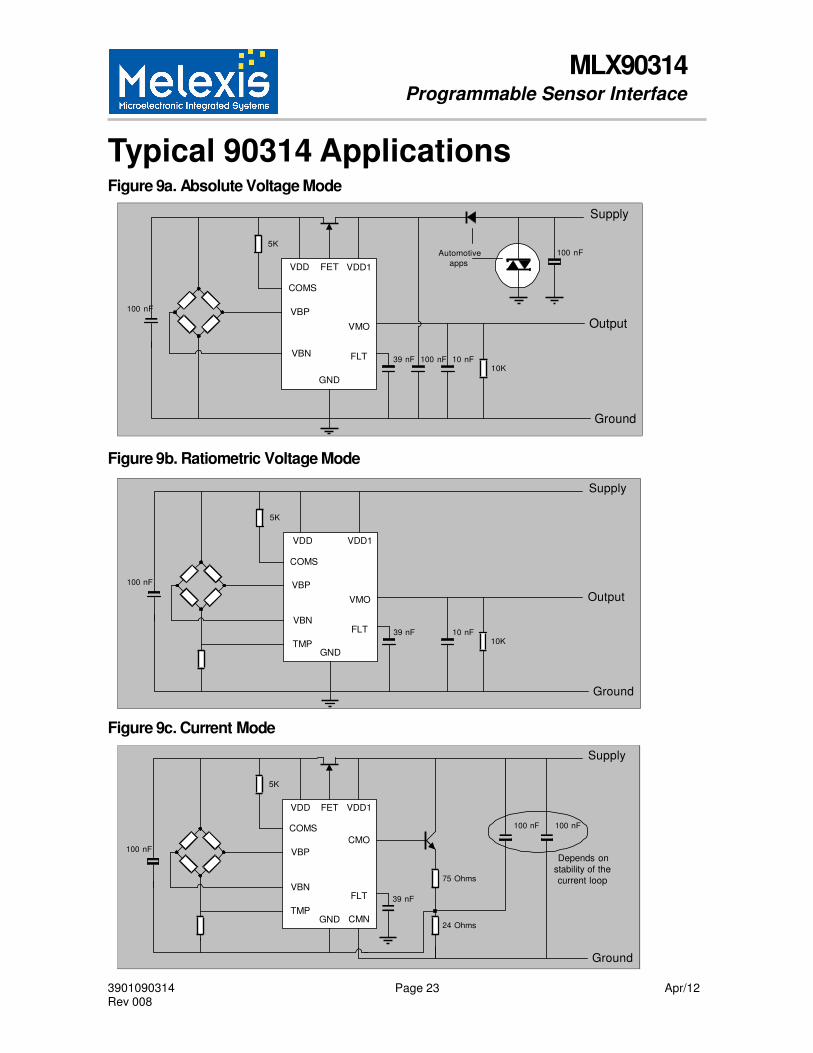
Typical 90314 Applications
Figure 9a. Absolute Voltage Mode
Supply
100 nF
5K
VDD FET
COMS
VBP
VDD1
VMO
Automotive
apps
100 nF
Output
VBN
GND
FLT 39 nF 100 nF 10 nF
10K
Ground
Figure 9b. Ratiometric Voltage Mode
Supply
5K
VDD VDD1
100 nF
COMS
VBP
VMO
Output
VBN
TMP
GND
FLT
39 nF
10 nF
10K
Ground
Figure 9c. Current Mode
Supply
5K
100 nF
VDD
COMS
VBP
VBN
TMP
FET
GND
VDD1
CMO
FLT
CMN
39 nF
75 Ohms
24 Ohms
100 nF 100 nF
Depends on
stability of the
current loop
Ground
3901090314 Rev 008
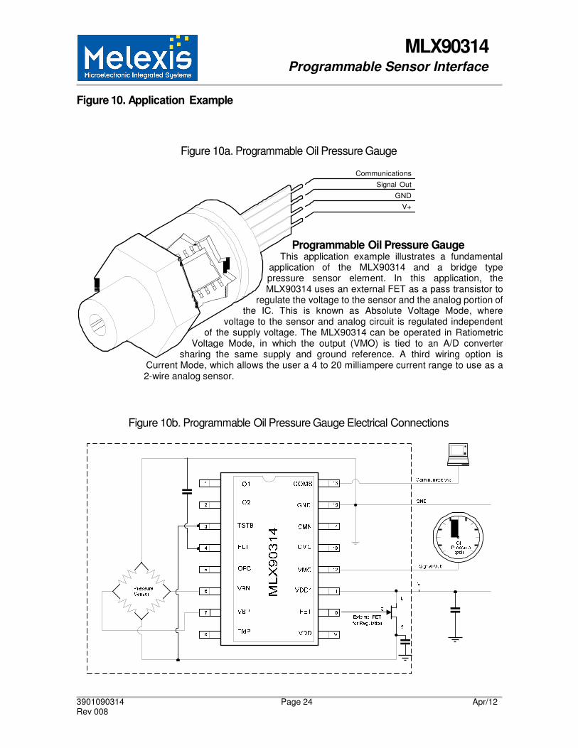
Figure 10. Application Exam
Figure 10
of theVoltag
sharing tCurrent Mode, w2-wire analog sen
Figure 10b. Program
MLXProgrammable Sensor
Page 24
mple
10a. Programmable Oil Pressure Gauge
Communications
Signal Out
GND
V+
Programmable Oil Pressure GThis application example illustrates
application of the MLX90314 and pressure sensor element. In this MLX90314 uses an external FET as a pa
regulate the voltage to the sensor and the the IC. This is known as Absolute Voltage
voltage to the sensor and analog circuit is regulathe supply voltage. The MLX90314 can be operated
ge Mode, in which the output (VMO) is tied to anthe same supply and ground reference. A third
which allows the user a 4 to 20 milliampere current ransor.
mmable Oil Pressure Gauge Electrical Connectio
MLX90314 Interface
Apr/12
Gauge ates a fundamental nd a bridge type
application, the pass transistor to analog portion of
age Mode, where ated independent ed in Ratiometric an A/D converter wiring option is ange to use as a
ons
MLX90314 Programmable Sensor Interface
3901090314 Rev 008
Page 25 Apr/12
Vo
lta
ge
(V
DC)
Vo
lta
ge
(in
mV
)
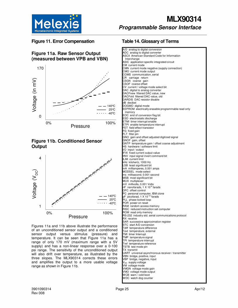
Figure 11. Error Compensation Table 14. Glossary of Terms
Figure 11a. Raw Sensor Output (measured between VPB and VBN)
170
140oC
25oC
-40oC
0
0% 100% Pressure
Figure 11b. Conditioned Sensor Output
4
140oC
25oC
-40oC
1
0% 100% Pressure
Figures 11a and 11b above illustrate the performance of an unconditioned sensor output and a conditioned sensor output versus stimulus (pressure) and temperature. It can be seen that Figure 11a has a range of only 170 mV (maximum range with a 5V supply) and has a non-linear response over a 0-100 psi range. The sensitivity of the unconditioned output will also drift over temperature, as illustrated by the three slopes. The MLX90314 corrects these errors and amplifies the output to a more usable voltage range as shown in Figure 11b.
A/D analog to digital conversion ADC analog to digital converter ASCII American Standard Code for Information
Interchange ASIC application specific integrated circuit CM current mode CMN current mode negative (supply connection) CMO current mode output COMS communication, serial CR carriage return CSGN coarse gain CSOF coarse offset CV current / voltage mode select bit DAC digital to analog converter DACFnew filtered DAC value, new DACFold filtered DAC value, old DARDIS DAC resistor disable dB decibel DOGMO digital mode EEPROM electrically erasable programmable read only
memory EOC end of conversion flag bit ESD electrostatic discharge ETMI timer interrupt enable ETPI enable temperature interrupt FET field effect transistor FG fixed gain FLT filter pin GNO gain and offset adjusted digitized signal GNOF gain, offset GNTP temperature gain / offset coarse adjustment HS hardware / software limit I/O input / output IFIX fixed current output value IINV input signal invert command bit ILIM current limit kHz kilohertz, 1000 Hz LSB least significant bit mA milliamperes, 0.001 amps MODSEL mode select ms millisecond, 0.001 second MSB most significant bit MUX multiplexer mV millivolts, 0.001 Volts nF nanofarads, 1 X 10⁻⁹ farads OFC offset control PC personal computer, IBM clone pF picofarad, 1 X 10-12 farads PLL phase locked loop POR power on reset RAM random access memory RISC reduced instruction set computer ROM read only memory RS-232 industry std. serial communications protocol RX receive SAR successive approximation register STC start A/D conversion Tdiff temperature difference Text temperature, external TMI timer Interrupt TMP temperature signal TPI temperature interrupt Tref temperature reference TSTB test mode pin TX transmit UART universal asynchronous receiver / transmitter VBN bridge, positive, input VBP bridge, negative, input VDD supply voltage VM voltage mode VMGN voltage mode gain VMO voltage mode output WCB warn / cold boot WDC watch dog counter
MLX90314 Programmable Sensor Interface
3901090314 Rev 008
Page 26 Apr/12
7.6
0
7.4
0
10
.65
10
.00
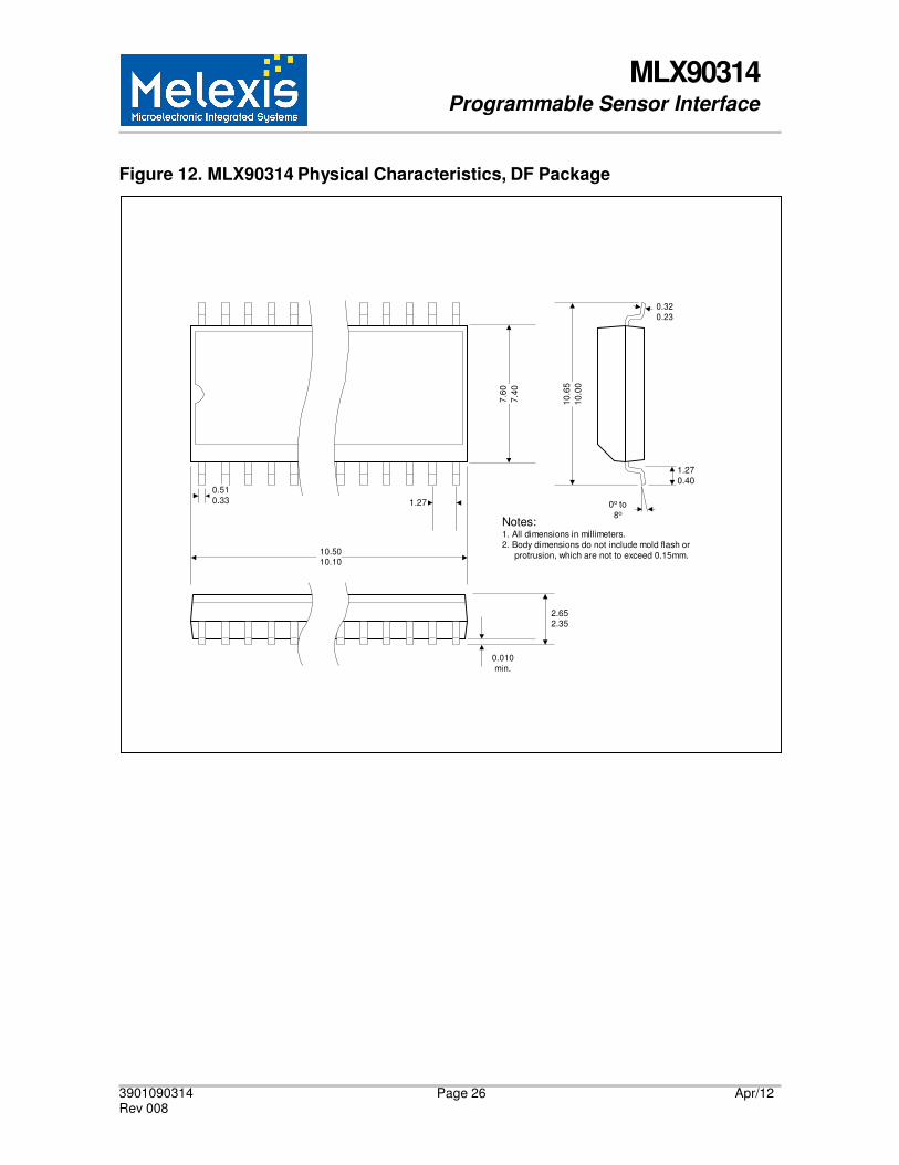
Figure 12. MLX90314 Physical Characteristics, DF Package
0.32 0.23
0.51
0.33
1.27
Notes:
0o to
8o
1.27
0.40
10.50 10.10
1. All dimensions in millimeters.
2. Body dimensions do not include mold flash or
protrusion, which are not to exceed 0.15mm.
2.65 2.35
0.010 min.

MLX90314 Programmable Sensor Interface
3901090314 Rev 008
Page 27 Apr/12
Standard information regarding manufacturability of Melexis products with different soldering processes Our products are classified and qualified regarding soldering technology, solderability and moisture
sensitivity level according to following test methods:
Reflow Soldering SMD’s (Surface Mount Devices)
• IPC/JEDEC J-STD-020
Moisture/Reflow Sensitivity Classification for Nonhermetic Solid State Surface Mount Devices
(classification reflow profiles according to table 5-2)
• EIA/JEDEC JESD22-A113
Preconditioning of Nonhermetic Surface Mount Devices Prior to Reliability Testing
(reflow profiles according to table 2)
Wave Soldering SMD’s (Surface Mount Devices) and THD’s (Through Hole Devices)
• EN60749-20
Resistance of plastic- encapsulated SMD’s to combined effect of moisture and soldering heat
• EIA/JEDEC JESD22-B106 and EN60749-15
Resistance to soldering temperature for through-hole mounted devices
Iron Soldering THD’s (Through Hole Devices)
• EN60749-15
Resistance to soldering temperature for through-hole mounted devices
Solderability SMD’s (Surface Mount Devices) and THD’s (Through Hole Devices)
• EIA/JEDEC JESD22-B102 and EN60749-21
Solderability
For all soldering technologies deviating from above mentioned standard conditions (regarding peak
temperature, temperature gradient, temperature profile etc) additional classification and qualification
tests have to be agreed upon with Melexis.
The application of Wave Soldering for SMD’s is allowed only after consulting Melexis regarding
assurance of adhesive strength between device and board.
Melexis is contributing to global environmental conservation by promoting lead free solutions. For
more information on qualifications of RoHS compliant products (RoHS = European directive on the
Restriction Of the use of certain Hazardous Substances) please visit the quality page on our website:
http://www.melexis.com/quality.aspx

MLX90314 Programmable Sensor Interface
3901090314 Rev 008
Page 28 Apr/12
Disclaimer
Devices sold by Melexis are covered by the warranty and patent indemnification provisions appearing in
its Term of Sale. Melexis makes no warranty, express, statutory, implied, or by description regarding the
information set forth herein or regarding the freedom of the described devices from patent infringement.
Melexis reserves the right to change specifications and prices at any time and without notice. Therefore,
prior to designing this product into a system, it is necessary to check with Melexis for current information.
This product is intended for use in normal commercial applications. Applications requiring extended
temperature range, unusual environmental requirements, or high reliability applications, such as military,
medical life-support or life-sustaining equipment are specifically not recommended without additional
processing by Melexis for each application.
The information furnished by Melexis is believed to be correct and accurate. However, Melexis shall not
be liable to recipient or any third party for any damages, including but not limited to personal injury,
property damage, loss of profits, loss of use, interrupt of business or indirect, special incidental or
consequential damages, of any kind, in connection with or arising out of the furnishing, performance or
use of the technical data herein. No obligation or liability to recipient or any third party shall arise or flow
out of Melexis’ rendering of technical or other services.
© 2012 Melexis NV. All rights reserved.
For the latest version of this document, go to our website at
www.melexis.com
Or for additional information contact Melexis Direct:
Europe, Africa, Asia: America: Phone: +32 1367 0495 Phone: +1 248 306 5400
E-mail: [email protected] E-mail: [email protected]
ISO/TS 16949 and ISO14001 Certified