Embed Size (px)
Citation preview

MITIGATION OF SOFT ERRORS IN ASIC-BASED AND FPGA-BASED LOGIC CIRCUITS
By
Varadarajan Srinivasan
Thesis
Submitted to the Faculty of the
Graduate School of Vanderbilt University
in partial fulfillment of the requirements
for the degree of
MASTER OF SCIENCE
in
Electrical Engineering
May, 2006
Nashville, Tennessee
Approved:
Professor William H. Robinson
Professor Bharat L. Bhuva

ACKNOWLEDGEMENTS
I would like to express my sincere gratitude to Professor William H. Robinson for
providing me an opportunity to work under him. I am deeply indebted to him, for his constant
encouragement and able guidance which has helped me to achieve my career objectives.
Working under him has been a great learning experience. His insights and wisdom has not only
helped me enrich my knowledge but also shaped my personality.
I would also like to thank Professor Bharat Bhuva for his invaluable suggestions and
support in this work. He has played a pivotal role in the development of this work and I would
always be indebted to him. I also sincerely thank Professor Lloyd Massengill, Professor Ronald
Schrimpf, Professor Tim Holman, Professor Robert Reed, Professor Robert Weller and Professor
Daniel Fleetwood for their invaluable advice and suggestions in group meetings. Their
exceptional knowledge and wisdom has greatly helped me in my academic progress.
I would also like to thank Defense Threat Reduction Agency, Boeing Radiation
Hardening By Design Program for funding this research work. A special thanks to Dr. Andrew
L. Sternberg for his invaluable suggestions and technical support. My sincere gratitude goes to
all fellow students in Radiation Effects and Reliability Group for making this an enjoyable and
resourceful place to work. I would also like to thank Adam Duncan of NAVSEA, Crane for his
useful contribution in the development of SEUTool without which this work would not have
been possible.
Finally, all this would not have been possible without the love and support of my parents
Mr. R. Srinivasan, Mrs. Kodhai Srinivasan and My sister Priya Srinivasan who have gone to
ii

great depths to provide me with the best education and I will forever be indebted to them. I
would like to dedicate this work to them.
iii

TABLE OF CONTENTS
Page
ACKNOWLEDGEMENTS............................................................................................................ ii LIST OF TABLES......................................................................................................................... vi LIST OF FIGURES ...................................................................................................................... vii Chapter I. INTRODUCTION ....................................................................................................................1 II. SOFT ERRORS IN LOGIC CIRCUITS ..................................................................................7 1) Conditions for Occurrence of Soft Errors ...........................................................................7 2) Charge Dissipation ..............................................................................................................8 (a) Adding Capacitance.......................................................................................................8 (b) Increasing Current Drive.............................................................................................10 3) Error Detection and Correction .........................................................................................13 (a) Built-In-Error-Detection (BIED) Techniques for a 16-bit ALU .................................15 (i) Berger Check Error Detection in ALU ..................................................................16 (ii) Remainder Check and Parity Check Scheme.........................................................18 a) Remainder Check for Arithmetic Instructions...................................................18 b) Parity Check for logical, shift and rotate instructions .......................................20 III. SEU MODELING IN ASIC LOGIC CIRCUITS...................................................................21 1) Identification of sensitive nodes ........................................................................................21 2) Probabilistic Modeling of SEUs in Combinational Logic and Latches.............................24 3) Simulation Details .............................................................................................................26 IV. IMPACT OF SELECTIVE HARDENING ON AN ASIC ALU ...........................................27 1) SEUTool Simulation Results.............................................................................................27 (a) Sensitive cross-section results .....................................................................................27 (b) Distribution of soft errors............................................................................................30 2) Hardening Sensitive Nodes ...............................................................................................30 (a) Selective Hardening of Sensitive Nodes by Transistor Sizing....................................32 (b) Impact of soft error distribution on SEU Sensitive cross-section ...............................33 3) Area Estimation .................................................................................................................34 4) Discussion..........................................................................................................................37
iv

V. PROCESSOR DESIGN FOR SEU MITIGATION IN FPGA BASED LOGIC CIRCUITS.39 1) Simulation Details .............................................................................................................39 2) Berger Check Processor Design ........................................................................................41 3) Remainder Check and Parity Check Processor Design .....................................................43 (a) Choice of Check Divisor .............................................................................................44 VI. IMPACT OF SEU MITIGATON ON AN FPGA-BASED ALU...........................................47 1) Simulation Results.............................................................................................................47 2) Discussion..........................................................................................................................50 VII. CONCLUSION ......................................................................................................................52 REFERENCES ..............................................................................................................................54
v

LIST OF TABLES
Table Page 1. Berger Check Symbol Equations for an ALU ..........................................................................17
vi
LIST OF FIGURES
Figure Page
1. Capacitive Hardened NAND2 Cell, Schematic and Layout................................................ 10 2. Two Input NAND gate (a) Standard Size Cell, (b) Current Drive Hardened...................... 12 3. Remainder check technique for error detection in arithmetic instructions .......................... 19 4. Identification of sensitive nodes using SEUTool................................................................. 23 5. Sensitive cross-section vs. charge........................................................................................ 28 6. Variation of sensitive cross-section with instruction ........................................................... 29 7. (a) Cumulative Distribution of Soft errors, (b) Soft Error Distribution............................... 31 8. Transient generated in AND-OR-INVERTER (a) Regular cell, (b) 3X sized cell.............. 31 9. Sensitive cross-section for combinational logic before and after hardening ....................... 33 10. (a) Sensitive cross-section for various levels of selective hardening, (b) Regions of Soft Error Distribution................................................................................. 34 11. (a) Percent Soft errors vs. Percent Nodes, (b) Area Increase vs. Percent Soft errors Removed ........................................................................................................... 35 12. Soft errors Removed Per Unit Area .................................................................................... 36 13. FLEX 10k Device Block Diagram (Courtesy: Altera’s FLEX10k Device Family Manual)................................................................................................................... 39 14. Block diagram of a single instruction issue Berger check processor.................................. 42 15. Block diagram of a single instruction issue error detection processor using Remainder and Parity check ............................................................................................. 43 16. Resource Utilization Chart for Various ALU Designs ....................................................... 47 17. Processor Design (a) Logic Element Comparison, (b) Clock Frequency Comparison ...... 48 18. Area Delay Product (a) Area-Delay comparison, (b) Constant Area Delay Contour......... 49
vii

CHAPTER I
INTRODUCTION
With ever decreasing device feature sizes, subsequent generations of semiconductor logic
circuits are more vulnerable to ionizing radiation effects when compared to their predecessors [1]
[2]. Soft errors, induced by single event strikes, are a major concern among logic designers,
regardless of whether they choose an ASIC implementation or an FPGA implementation. In an
ASIC design, a single event strike can corrupt the data processed by the circuit [3] [4]. However,
in an FPGA design, a single event strike can not only corrupt the data but also affect the circuit
functionality [5] [6]. Therefore, mitigation strategies must be employed in radiation-prone
environments to ensure proper functionality of both ASIC-based and FPGA-based logic circuits.
Traditionally, soft errors in memory circuits have been a greater concern compared to soft
errors in combinational logic for the same technology, since memories contain the largest density
of vulnerable bits [7] [8]. Error detection and correction (EDAC) codes have been extensively
used to address single event upsets (SEUs) in memory [9] [10]. However, future technologies
with smaller feature sizes and higher operating frequencies will cause an increased soft error rate
in combinational logic circuits that will significantly contribute to the overall soft error rate of
the system [7] [11-15]. In an ASIC design, functionality of the combinational circuit has a
significant influence in the soft error rate and sensitive cross-section. All the cells in the ASIC
are not equally sensitive [16-20]. In contrast, the highly-regular arrangement of the FPGA fabric
can create equal vulnerability across the circuit regardless of the particular function being
implemented.
1

Some techniques commonly used for hardening ASIC combinational logic are aimed at
reducing the effective cross-section of the sensitive cells by either replicating the cells (spatial
redundancy) or using multiple sampling of the same node (temporal redundancy) at different
time intervals [21-24]. However, redundancy techniques have huge area/performance penalties.
In addition, the voter circuit used to filter out the incorrect output is sensitive to ion strikes. Other
techniques used for hardening ASIC combinational logic increase the charge required to generate
a single event transient pulse and hence the threshold critical charge, Qcritical. The Qcritical of a
node can be raised either by increasing the transistor current drive (increasing the W/L ratios of
the transistors) or by adding additional capacitance at the output node of the logic gate [23-25].
The above mentioned techniques for increasing Qcritical are simple in implementation, but involve
huge area, performance, or power penalties if used to harden all the cells because area, power,
and speed are proportional to the current drive within the cell [23] [24].
In FPGA design, the mitigation strategy used should be capable of eliminating all types
of errors. The following are some of the common soft errors in SRAM based FPGAs:
• Configuration Memory Upset: Configuration memory defines the circuit functionality.
It basically consists of an SRAM array storing truth table data of all logic functions. An
SEU in one of the configuration memory SRAM cell changes the logic function. The
circuit now behaves incorrectly. Based on the type of logic circuit implemented by the
configuration memory, an SEU in configuration logic can lead to one of the following
errors:
(1) Persistent Data Errors: Persistent errors are data errors resulting from a
configuration memory upset causing incorrect functionality. In state machines and
counters, a configuration memory upset can throw the circuit into an incorrect state. In
2

spite of correcting the circuit functionality by scrubbing, the circuit cannot return to its
original state. This may result in execution of a wrong instruction, execution of an infinite
loop etc. Regardless of the SEU correction scheme employed, these errors will never be
flushed out of a system. Only with additional intervention (e.g., using a reset signal) will
the system ever recover.
(2) Non-Persistent Data Errors: Non-persistent errors are also data errors resulting from
a configuration memory upset, but they can be flushed out of the system. In
combinational logic circuits such as an Arithmetic Logic Unit (ALU), a configuration
memory upset may result in incorrect ALU functionality. However, by scrubbing the
configuration memory, correct functionality can be restored.
From now onwards any reference to configuration memory error implies non-persistent
data errors, as persistent data errors cannot be rectified by techniques discussed in this
thesis.
• Single Event Transient (SET) Data Errors: Data errors also occur due to generation of
SETs in combinational logic components such as multiplexers, Look-Up-Table (LUT)
routing transistors, routing channels, etc. SETs originating from these block can get
latched and result in a data error even when the circuit is functioning properly. Such
errors are difficult to isolate and rectify. Techniques presented in this thesis would
address SET induced data errors.
SRAM-based FPGAs are cheaper, offer design flexibility, and on-site correction
capabilities, but they are more sensitive to SEUs compared to Antifuse FPGAs. Antifuse-based
FPGAs offer significant reliability against SEU’s, but their inability to be re-programmed makes
them useful only for specific applications. Techniques such as scrubbing and partial
3

reconfiguration have been effectively used to eliminate soft errors induced by configuration
memory upsets [26]. The memory scrubbing technique mitigates soft errors by periodically
reloading the configuration bits. In partial reconfiguration, the configuration memory is provided
with post-configuration operations for both read-back and write-back. In partial reconfiguration,
soft errors can be detected by a read-back operation followed by a bit-by-bit comparison of the
retrieved data frame [26].
A standard mitigation strategy for both ASIC and FPGA implementations is triple
modular redundancy (TMR). In ASIC implementations, TMR in conjunction with a hardened
voter circuit is used to remove single points of vulnerability (i.e., all paths to the output are
triplicated). In SRAM based FPGAs, TMR can be used to address single-bit data errors (SET,
Persistent, Non-Persistent) occurring in one design unit [27] [28]. However, TMR cannot handle
errors in voter circuit and multiple errors in redundant units. As the probability of a multiple bit
upset is significantly low, TMR offers considerable reliability to all error sources. Further,
modern TMR designs also use redundant voter circuits to reduce voter vulnerability. However,
there is a significant area and power penalty (approximately a factor of 3X – 3.5X) associated
with TMR [29].
This thesis focuses on developing techniques to mitigate soft errors in ASIC and FPGA
based combinational logic circuits without incurring the 3X penalties of TMR techniques. For
ASIC SEU mitigation, a selective hardening approach is used on the most sensitive cells in the
circuit. The selective hardening methodology for the combinational logic is implemented on a 4-
bit ALU data path of the LEON2 SPARC V8 processor Integer Unit [30] [31]. The hardening
process involves three steps: (1) identification of sensitive nodes, (2) ranking of nodes based on
the sensitivity, and (3) hardening the most sensitive nodes selected from the soft error
4

distribution. In order to harden the sensitive cells, the drive strengths of the NMOS and PMOS
transistors in the cell were increased by increasing their sizes. The increase in drive strength
sinks the collected charge quickly thereby, reducing the transient pulse width. However, this
results in an increase in the area of the cell [23-25]. The impact on circuit area by hardening the
sensitive cells by this technique is discussed.
In FPGA design, Feed-Forward Logic Circuits (combinational logic) are designed with
Built-In-Error-Detection (BIED) using error detection and correction codes. BIED can detect
both SET data errors as well as non-persistent errors [32] induced by configuration memory
SEUs, while incurring less than 3X area penalty. A check symbol is calculated using the input
data symbols. This input check symbol is compared with the check symbol calculated from the
feed-forward logic output. A SEU strike in the configuration memory would affect the
functionality of the feed-forward logic circuit causing a change in the input or the output check
symbol. This mismatch in the check symbol would generate an error signal. The error signal can
be used to reconfigure the configuration memory to fix the discrepancy in the circuit
functionality. Further, the error signal can be fed back to the state machine to regenerate (reissue)
the instruction and data to recover the correct output. Performance of the system is slightly
compromised by re-issuing the instruction and data on the detection of an error, rather than
fixing the SEU by TMR. The area gain is significant compared to the slight compromise in
performance.
This Thesis is organized into following chapters:
• Chapter 2 gives an overview of the hardening by increasing the drive strength and use of
error correction codes to mitigate soft errors.
5

• Chapter 3 discusses the selective hardening methodology in a 4-bit ALU slice of a
LEON2 processor integer unit.
• Chapter 4 presents the results of selective hardening methodology.
• Chapter 5 discusses the various BIED schemes for error detection and correction in
FPGA based feed-forward logic circuits.
• Chapter 6 presents the area/performance results of the various BIED techniques.
• Chapter 7 concludes the discussion of soft error mitigation in ASICs and FPGAs.
6

CHAPTER II
SOFT ERRORS IN LOGIC CIRCUITS
1) Conditions For Occurrence Of Soft Errors [23]
Single event transients (SETs) are transients generated in an electronic circuit due to the
interaction of ionizing particles with components in the circuit. A charged particle incident on a
circuit node loses energy which creates electron-hole pairs along the path traversed by the
incident ion. The electric field present along this charge track generates a current transient in the
associated node, resulting in either pull-up or pull-down of the legitimate logic signal at the
node. These current pulses can create transient errors in the circuit. The necessary set of
conditions under which a SET that originates in combinational logic can result in a static bit error
have been described as follows [11] [33]:
(1) A single event which generates a voltage transient capable of propagating into the
local circuitry;
(2) A “critical path” or open logic path existing between the hit node and a latch,
allowing the hit node to control the logic state of the path;
(3) A transient pulse with amplitude and duration sufficient to write a terminal latch; and
(4) Coincidence of the pulse arrival and a latch write-enable state.
This set of conditions provide a number of considerations and opportunities for hardening
combinational logic against transient errors which are different from those used for bit upsets in
7

sequential logic. In the following section some of the traditional techniques for mitigating soft
errors in combinational logic are presented.
2) Charge Dissipation
Charge dissipation methods include: (1) adding capacitance or (2) increasing the circuit’s
current drive so that the critical charge required to produce any given upset pulse is increased.
(a) Adding Capacitance
In capacitance filtering, additional capacitance is added to the sensitive node such that the
critical charge (QC) required to upset the node increases [23] [24]. In 0.18um technology, for a
minimum sized NAND Gate, the additional capacitance required can be determined. For a
NAND Gate, assuming the capacitance to be dominated by the gate capacitances of load, we can
estimate the capacitance at the node under strike using following equations [34]:
LNode CC = (1)
nnoxgn LWCC ××= and ppoxgp LWCC ××= (2)
For 0.18um TSMC [35], Cox = (8.854 * 10-12 / 4.1 * 10-7) = 21.59 uF/cm2 [35]. Cgn, Cgp,
can be calculated for a minimum sized NAND gate. Let Wn = Ln = 0.18um, Lp = 0.18um and Wp
= 0.45um.
fFCfFC gpgn 18,7 ==
Assuming an NAND load (FO = 2) with same transistor sizes.
fFfFfFCCC gpgnL 50)187(2)(2 =+=+=
8

The critical charge (Qc) required to upset the node is given by the following equation [23] [24],
2ddL
CVC
Q×
= (3)
A simple relationship for calculating the charge deposited by an ion is given by equation (4) [23]
[36],
where, Q is the charge in picocoulombs, LET is the Linear Energy Transfer in MeV-cm /mg of
the incident ion, and D is length in um of the ion path over which the charge is deposited in an
element of the circuit. An average LET value of 40 MeV-cm2/mg is
For a 1.8V technology, Qc = 45fC, i.e. charge required to create an upset is 45fC approximately.
DLETpCQ ××−×= 21003.1)( (4) Coll
2
often used as a specification
since it corresponds to a point of dramatic reduction in the heavy ion LET spectrum in space
[37]. A collection length, D, of 1 um represents a reasonable order of magnitude for conventional
logic circuits. The collected charge, QColl, in this case would be given by
pCumgm
cmMeVColl
22 −−
The capacitance required to increase the critical charge Q
Q 42.01401003.1 =∗∗∗=
be calculated from the
following relation.
c to 0.42 pC can
newnewc CQ −
Using equation 5,
oldoldc CQ=− (5)
oldnew CC (6) fCfC 10
45420
≅=
9

10
Such a huge capacitance will result in significant area, speed and power penalties. A
representative schematic and layout for a NAND gate are shown in Figure 1 [23].
(b) Increasing Current Drive
An alternative charge dissipation method is to use transistors with higher current drive
25] NMOS and PMOS quickly dissipates the collected charge,
ereby
Figure 1: Capacitive Hardened NAND2 Cell, Schematic and Layout [20]
[23- . Larger drive strength of
th reducing the effective transient pulse width. This can be better understood from the
following equation, [23] [24]
WidthPulseItIdtIQ avgavgColl ×=×≈= ∫ Δ. (7)
For a given QColl, as we increase the drive strength of the transistors, Iavg increases. The increase
in Iavg is compensated by a decrease in the pulse width as area under the curve is con∫ dtI. stant.

Increasing the drive strength hardens the circuit by causing the SET to fail condition (3)
in Section I. For 0.18um technology, minimum transient pulse width necessary to get latched is
ssumea d to be 200ps. The drive needed to sink a charge of 0.42 pC in 200ps is given by equation
8 [23] [24],
mApCCollQ
I 1.242.0
≅== (8) psWidthPulse 200
For 0.18um TSMC process, the current drive of an NMOS can be calculated using the
following equation [34],
( )2'thgsnD VVwkI −⎟
⎞⎜⎛= (9)
l ⎠⎝
Assuming Wn = 0.36um, approximate values for K’n and Vth can be obtained from [35].
Using these values, approximate value of ID can be determined as follows:
( ) mAuAVAID 6.0064.5845.08.12108.172 222
6 ≈=−∗∗∗= − V
As we know that ID ∝ Wn, the NMOS transistor width required for a drive strength of
2.1mA can be calculated from the following relation,
new
old
newD
oldD WI=
−
− (10) WI
From the above relation, the NMOS width Wnew corresponding to drive strength of
2.1mA is given by,
oldoldnew WWmAW 5.31.2=×= (11)
mA6.0
Figure 2 shows the layout changes that would be necessary for a simple NAND gate [23].
11

Figure 2: Two Input NAND gate (a) Standard Size Cell, (b) Current
Increasing the capacitance of the node will result in significant speed and power penalties
add
Drive Hardened
in ition to the area penalty [23] [24]. Large values of capacitances can also filter out
legitimate logic signals in high frequency circuits. Increasing the transistor current drive might
result in area and power penalty, but the area penalty can be minimized by selectively hardening
the sensitive cells [23] [24]. Further, increasing the drive strength of a gate would require
increasing the drive strengths of other gates driving the gate under consideration. This will
further increase the area and power requirements. This thesis focuses on hardening by transistor
12

sizing as the capacitance technique involves significant area, speed and power penalties.
However, the above mentioned techniques are applicable only for hardening ASIC logic circuits.
In FPGA logic circuits the combinational logic is implemented either as a look up table
(LUT) or as a multiplexer logic. In such a design it is very difficult to isolate soft error sensitive
LUTs or multiplexers. Further the FPGA fabric is a uniform design and it is very difficult to vary
device sizes in a FPGA fabric to improve reliability. Hence in FPGA logic circuits a different
mitigation technique is necessary. In the next section we discuss error detection and correction
codes which form the basis for soft error mitigation in FPGAs.
3) Error Detection And Correction [38-42]
Spatial and temporal redundancies rely on the use of significant redundancy in space or
time to perform error detection and correction. However, in some applications less redundancy is
adequate for detection and correction of errors. In these schemes, information redundancy and
encoding are utilized such that in the presence of errors, the information is internally
inconsistent, enabling error detection and correction implementations.
Error detection and correction coding theory is the most widely developed domain for
detection and recovery in digital systems. This typically requires less redundancy than other
detection and correction schemes. Replication techniques like TMR (Triple Mode Redundancy)
is effective in detection and correction capability, but has large size, power, and cost implications
for some types of applications, whereas Error Correction Coding (ECC) provides a more
effective solution [38-43]. Error detection and correction codes can vary widely in detection and
correction capabilities, code efficiency, and complexity of encoding and decoding circuitry. The
13

simplest form is the use of an additional parity bit to provide single error detection in buses,
registers, and memory.
A code’s error detection and correction properties are based on its ability to partition a set
of 2n, n-bit words into a code space of 2m code words and a non-code space of 2n - 2m words [40]
[41]. The most common block code used in memory systems is the single error correcting,
double error detecting (SEC-DED) Hamming code [38] [44]. It provides single bit error
correction and double bit error detection. A characteristic of error detection and correction codes
is the Hamming distance between words in the code space; the single correcting, double
detecting code has a Hamming distance of four [44].
If “C” is the number of errors to be corrected, “D” is the number of errors to be detected
and “d” is the hamming distance (number of differing bits between adjacent code words), then
“d” can be expressed as follows [38] [44],
1++≥ DCd (12)
For a single error correcting code (C = 1), double error detecting code (D= 1), the hamming
distance must be
4121 =++≥d
More powerful codes may be constructed by using appropriate generating polynomials.
Cyclic redundancy checks, other cyclic codes, and convolutional coding schemes are
used to detect errors in serial data transfer interfaces and storage media [38-40]. However, these
types of codes are useful only in data storage and transmission systems, such as memory and
data networks. In arithmetic processing circuits, such as an ALU, these codes are incapable of
detecting errors as two data symbols are subjected to an arithmetic/logic operations resulting in a
new data symbol which cannot be uniquely expressed as the combination of inputs [40] [41]
14

[45]. In such systems, a different error coding strategy is required. Arithmetic codes such as AN
codes [40] [41], Residue codes and Inverse Residue codes have been extensively used for error
correction and detection in arithmetic circuits, but these codes are useful only for error detection
in arithmetic circuits such as adders, subtractors and multipliers [45]. Arithmetic codes are
preserved only under arithmetic operations and they are not valid for logical and shift operations.
Hence, it is much more difficult to detect errors in ALU circuits, compared to data transmission
and storage circuits. This section would focus on error detection and correction in an ALU. Two
different error coding strategy are used to design a single instruction issue processor with Built-
In Error Detection Schemes (BIED).
(a) Built-In-Error-Detection (BIED) Techniques for a 16-bit ALU
In this thesis, we apply the idea of using systematic separate codes to detect soft errors in
ALUs. In separate codes, the information and data symbols are transmitted through separate
channels. The Check symbols and Information symbols can be subjected to different operations
to detect the soft error. Three different ALU designs were realized on the target device (Altera’s
Flex EPF10k70RC240) to compare the area and performance for (1) Berger Check ALU, (2)
Remainder and Parity Check ALU and (3) TMR ALU. Berger check codes [46] [47] can be
applied to all the ALU operations. The check symbols calculated from the Berger check
operation are capable of detecting errors in ALU arithmetic, logical, shift and rotate instructions
[46] [47]. The Berger check code represents a global coding strategy, i.e., a common coding
strategy valid for all the ALU instructions. The second BIED technique categorizes ALU
instructions into groups based on the nature of the operation performed on the data symbols. The
instruction groups are (1) arithmetic, (2) logical, (3) shift, and (4) rotate. A remainder check is
15

used for error detection in arithmetic instructions. A simple parity check is implemented for error
detection in logical, shift, and rotate instructions. The two BIED techniques (Berger check,
Remainder and Parity checks) are compared with a TMR ALU. All three versions of the ALU
were used to design a single instruction issue processor.
(i) Berger Check Error Detection in ALU
Consider the addition of two n-bit numbers, X = (xn, xn-1… x1) and Y = (yn, yn-1… y1) to
obtain the sum S = (sn, sn-1… s1). The internal carries generated by the addition is represented as
C = (cn, cn-1… c1), where xi, yi, si, ci ∈ {0, 1}. The ith bit operation of the two operands is given
by the following equation [46] [47].
outcisincinciyix ++=++ (13)
outcincis ++= )(
Let N(X) represent the number of 1’s in the binary representation of the data symbol X. Then
N(xi) ≈ xi. Using this notation the Lemma is presented in [46] [47] as
)()()()( CNoutcSNincYNXN ++=++ (14)
Where, cin = input carry and cout = cn.
There are two possible Berger check symbol encoding schemes. The check symbol can
be calculated from the number of 0’s in the binary representation of the information symbol (or
the complement of the binary representation of the number of 1’s). It is a usual practice to use
the first encoding scheme for check symbol calculation. For an n-bit number whose Berger check
symbol is Xc, Xc = n – N(X), where N(X) is Number of 1’s in X. Similarly, Yc = n – N(Y), Sc = n
– N(S) and Cc = n – N(C). Rearranging and Substituting for N(X), N(Y), N(S) and N(C) in
equation 14 we get [46] [47]
16

( ) ( ) ( ) ( )CoutCinCC CncSncYnXn −++−=+−+−
outccCinccYcXcS +−−+= (15)
Where Xc, Yc and Cc represent the number of 0’s in the binary representation of X, Y and
internal carries C.
Similarly for logical operations AND (∧), OR (∨) and XOR (⊕) the Berger check symbol
can be calculated from the following equations [46] [47],
)iyi(xiyixiyix ∨−+≡∧ (16)
)iyi(xiyixiyix ∧−+≡∨ (17)
)iyi(xiyixiyix ∧−+≡⊕ 2 (18)
A similar analysis was performed for some common ALU arithmetic, logic, shift, and
Table 1: Berger Check Symbol Equations for an ALU [7-8]
Xc, Yc = No. of 0’s in data X and YCin = Carry in, Cout = Carry out
Cc = No. of 0’s in internal carries, n = No. of data bits Cc’ = n2 – n – N(C’), where N(C’) = Sum of all internal carries in a
array multiplier
Berger Check of result is same as operand
Rotate left/right
Sc = Xc – Cin + CoutShift-Right/Shift-Right
Sc = Xc + Yc – 2(X and Y)c + nXOR
Sc = Xc + Yc – (X and Y)cOR
Sc = Xc + Yc – (X or Y)cAND
Sc = nXc + nYc – Xc*Yc – Cc’ MUL
Sc = Xc –Yc – Cc – Cin + Cout + nSUB
Sc = Xc + Yc – Cc –Cin +CoutADD
Berger Check SymbolALU Operation
17

rotate operations in [46] [47]. Table 1 presents the summary of Berger check symbol equations
for some basic ALU operations. In Chapter V, the design of a 16-bit single instruction issue
processor using the equations in Table 1 is discussed
(ii) Remainder Check and Parity Check Scheme
a) Remainder Check for Arithmetic Instructions
Remainder check codes are based on the principle that a remainder calculated for the
value X and value Y in an ALU would be preserved through the arithmetic ALU operations. The
mathematics behind the remainder check codes is presented below.
Let us assume that the ALU input data consists of two numbers, X and Y, each n bit long.
Then, X and Y can be represented as:
01221 ..... xxxxxX nn −−=
01221 .... yyyyyY nn −−=
Also, assume that the check divisor used for generating the remainder is an m-bit number P,
where:
01221 .... pppppP mm −−=
and m < n. The remainder obtained when X (or Y) is divided by P is given by:
PYR
PXR YX == & , where
01221 .... rrrrrR mmX −−= and ,0
,1
,2
,2
,1 .... rrrrrR mmY −−=
For all ALU arithmetic operations, the ALU output follows the appropriate mathematical
function, given by:
18

YopXS )(= , where op = +, -, *, (19)
The remainder check code, RCCin, calculated from RX and RY also follows the same mathematical
function, i.e.
PRopR
R YXCCin
)(= (20)
RCCout is the remainder check symbol calculated from the ALU output. RCCout is calculated by
dividing the ALU output S from the check divisor P.
PSRCCout = (21)
The error signal generated by the comparator is given by the following function:
{ CCoutCCinCCoutCCin
RRRRSignalError ≠
== ,1,0 (22)
The block diagram in Figure 3 illustrates the error detection technique using Remainder check
codes.
YP
XP R op R
PX Y⎛
⎝⎜⎞⎠⎟⎧
⎨⎪
⎩⎪
⎫⎬⎪
⎭⎪
CHECKCOMPARATOR
ALUSP
RX
RY
RCCin
RCCout
X
YS
ErrorSignal
Extra Hardware
YP
XP R op R
PX Y⎛
⎝⎜⎞⎠⎟⎧
⎨⎪
⎩⎪
⎫⎬⎪
⎭⎪
R op RP
X Y⎛⎝⎜
⎞⎠⎟⎧
⎨⎪
⎩⎪
⎫⎬⎪
⎭⎪
CHECKCOMPARATOR
ALUSPSP
RX
RY
RCCin
RCCout
X
YS
ErrorSignal
Extra Hardware
Figure 3: Remainder check technique for error detection in arithmetic instructions
19

b) Parity Check for logical, shift and rotate instructions [38-40]
For error detection in logical, shift, and rotate instructions, a parity bit is calculated
from the information symbols in X and Y. Parity is chosen such that the total parity of the
information and the parity symbol is even. In a shift instruction, the number of 1’s remaining
after the shift operation will only contribute to the parity. In rotate instructions, the parity does
not change throughout the ALU operation. If the input data and the output data matches, error
signal is set to “low”, whereas incase of a mismatch error signal is set to “high”.
20
CHAPTER III
SEU MODELING IN ASIC LOGIC CIRCUITS
1) Identification Of Sensitive Nodes
A particle strike on a combinational logic circuit can alter the logic value produced by the
circuit. However, the transient change caused by the particle strike will not usually affect the
computational results unless it is captured by the sequential elements in the circuit. All the
transients originating in a combinational logic node may not propagate to the output port or a
latch. Propagation of a transient to the output depends upon the following masking effects [15-
18] [20]:
(a) Logical masking occurs in the absence of an active path from the sensitive node to the
output-ports/latches.
(b) Latch-window masking arises when the transient generated from a sensitive node reaches
the latch/flip-flop at an instant other than the clock window for latching.
(c) Electrical masking causes the generated transient to attenuate as it passes through the
active path from the sensitive node to the output-port/latches.
These masking effects can result in a significantly lower soft error rate in combinational
logic circuits [48]. However, as the feature size decreases and the combinational logic on a chip
increases (e.g., to support more functionality or more instructions), these masking effects may
diminish. For example, at higher operating frequencies, number clock edges available for the
transient to get latched increases. This effect reduces the latch window masking probability [49].
21

The above factors would contribute to the increase in the sensitivity of the combinational logic in
advanced technology nodes.
In order to minimize area, power, or speed penalties, a selective hardening methodology
is used by identifying the most sensitive nodes. Test circuit is an integer unit from the LEON2
SPARC V8 processor [30], and a CAD tool named SEUTool [16] is used to simulate single-
event strikes on every node in the circuit. SEUTool uses SPICE and VHDL propagation
simulations to identify sensitive cells in a logic circuit. In [19] and [20], a methodology to
identify sensitive nodes has been proposed. In [19], the algorithm proposed does a worst-case
estimation by assuming all the strikes would generate a transient of critical amplitude. Input
conditions to the transistors in a logic gate influence the nature of the generated transient. A
transient which pulls the output node voltage down to ground (0V) would not have any effect if
the other input conditions already drive the output voltage to 0V. Hence, test vector influences
the generation of voltage transient in a node. VHDL propagation simulations are used to identify
test vectors for which a logic node has an active path to output. SPICE simulations determine the
probability of transient generation at the associated node.
Any single-event transient that propagates to an internal latch is a soft fault. However, if
the transient propagates to an observable output port, it is termed as a soft error [50]. SEUTool
generates a list of nodes that produce soft faults and soft errors for a given set of input
instructions and data.
The SPICE simulations are performed taking into consideration accurate loading
information of the logic block under test to determine the transient characteristics. The flowchart
in Figure 4 illustrates the process flow in the identification of the vulnerable nodes.
22

Figure 4: Identification of sensitive nodes using SEUTool
In order to illustrate the selective hardening methodology, a 4-bit data path was hardened
within the LEON2 integer unit. This circuit includes all components associated with the least-
significant four bits (two data inputs and one data output of the 4-bit ALU slice). The 4-bit data
path consists of 210 gates and 12 flip flops which form a total of 222 nodes. Since it is a
common practice to design data paths by duplicating smaller instances, such as a 4-bit data path,
this hardening methodology could be replicated for other instances to harden the whole 32-bit
integer unit. An exhaustive set of logic simulations were performed for the 4-bit ALU bit slice by
executing the following ALU instructions: ADD, SUB, AND, OR, XOR, XNOR,
SHIFT_RIGHT, SHIFT_LEFT. All possible 256 data inputs were applied to the 4-bit ALU while
executing the above mentioned instructions. Logical bit flips were introduced in every node in
the circuit to identify the propagation paths to the output nodes. For SHIFT_LEFT and
SHIFT_RIGHT instructions, only 90 data input combinations are required to test all the shift
distances. The results of the exhaustive simulation set are used to determine the logic masking
probability PCNError for every node in the circuit [16-18] which is described in the next section.
23

To estimate the sensitive cross-section using SEUTool, probability equations presented in
[16-18] were used. Strikes on combinational logic propagating to a storage elements and direct
strikes on latches were simulated. A brief summary of the probability equations used in SEUTool
[16-18] is given below.
2) Probabilistic Modeling Of SEUs In Combinational Logic And Latches
There are three inherent assumptions in SEUTool modeling: (1) operation of the circuit is
synchronous, (2) the probability of two single-event (SE) strikes to a particular node on the same
clock cycle is 0, and (3) electrical masking is neglected. The reason for ignoring electrical
masking is due to the difficulty in performing SPICE transient propagation simulations in large
processor circuits. VHDL logic propagation simulations are used to identify propagation paths.
Worst case estimate for sensitive cross-section is obtained by ignoring electrical masking effect.
Using the above assumptions and given an SE hit for collected charge Qcoll anywhere in the
circuit during a particular clock cycle C, then PC,NSF, the probability that the SE hit occurs at
node N and causes a soft fault in the clock cycle C, is given by equation 23 [16-18],
StorageLN
opPrLNC
PulseN
SFNC PDPP *,,,, ××= (23)
where, given an SE strike depositing QColl at a random location anywhere within the total circuit
area, PNPulse is the probability that node N will generate an output perturbation above the logic
noise margin and thus produce an erroneous logic signal. DC,N,LProp is a deterministic measure
that, given an erroneous signal originating at node N during clock cycle C, the signal will
propagate to latch L. The probability PN,LStorage is the probability that a randomly arriving logic
signal along an active path from N to L will corrupt the latch L. PN,L*Storage is the probability of
storage for the latch L* which is the maximum for all latches with active paths from N. PN,L*Storage
24

corresponds to the latch-window masking probability. The probability that a random SE hit
occurs at node N and causes an observable error at the output pin during the clock cycle C is
given by equation 24 [16-18],
EventPostNCinSF
SFNC
ErrorNC DPP −×= ),(,, (24)
where DSF in {C,N}Post-Event
is a deterministic measure that, given a soft fault originating from node
N during clock cycle C, the soft fault (SF) will appear as an error at one of the circuit outputs
during subsequent clock cycles. This is repeated for all the cells in the circuit and the total
sensitive cross-section is estimated for all the combinational logic cells in the circuit using
equation 25 [16-18],
∑ ×− =
CellsAll
AreaCellSensitiveError
NCsectionCross P , (25)
The above probability formulae are used to estimate sensitive cross-section with the aid
of SEUTool and SPICE simulations. The sensitive cell area is assumed to be the drain area of the
cell transistors. Figure 4 shows the SEUTool flow for sensitive cross-section estimation. The
circuit-under-test and the corresponding test bench is the input to SEUTool. SEUTool edits the
netlist of the circuit under test and performs logic propagation simulations to determine the
deterministic factors DC,N,LProp and DSF in {C,N}
Post-Event. Logical bit-flips are simulated on every
node in the circuit for all possible data input combinations. DC,N,LProp is calculated as the number
of times a logical bit-flip propagated to a latch divided by the total number of simulations.
Similarly, DSF in {C,N}Post-Event is given by the number of times a logic-bit flip caused an error at the
output port divided by the total number of simulations performed. For the 4-bit ALU, a total of
256 simulations were performed for every node in the circuit to determine DC,N,LProp and DSF in
{C,N}Post-Event.
25

The propagation simulations determine a list of library cells that might create soft errors.
These cells are then simulated in SPICE by striking all the nodes in the cell (both internal and
external). The SPICE simulations are used to identify data input combinations that generate a
transient greater than the threshold (which is assumed to be 0.5Vdd). The probability PNPulse
is the
ratio of the number of times the transient exceeds the threshold over the total number of SPICE
simulations for the cell. This probability PNPulse, combined with PN,L*
Storage is used to calculate the
probability of latching.
A similar analysis is performed for direct strikes on latches. Strikes within the vulnerable
window of the latches are considered to estimate the sensitive cross-section.
3) Simulation Details
The LEON2 is a synthesizable VHDL model of a 32-bit processor compliant with the
SPARC V8 architecture. The model is highly configurable and particularly suitable for system-
on-a-chip (SOC) designs. The LEON2 SPARC V8 processor was designed under contract from
the European Space Agency and has successfully been used in various commercial and research
endeavors [30] [31]. The standard version of the LEON2 is made freely available in full source
code under the GNU Lesser General Public License (LGPL).
The simulations performed in this thesis use the integer processing unit only, which
consists of a five-stage pipelined integer processor. The integer unit was synthesized with ASIC
libraries developed by the Illinois Institute of Technology (IIT) using 0.18µ TSMC process
information [51].
26

CHAPTER IV
IMPACT OF SELECTIVE HARDENING ON AN ASIC ALU
1) SEUTool Simulation Results
SEUTool is a VHDL-based soft error simulator which analyzes SET propagation after the
occurrence of a single event strike. SEUTool logic simulations were performed on the 4-bit ALU
data path to determine the number of times a node has an active path to the output and the
masking probabilities associated with the transient propagation. SPICE simulations were
performed on the library cells for a range of charge from 20fC to 1600fC. The sensitive cross-
section is evaluated for both the combinational logic and the latches in the 4-bit ALU bit slice.
The sensitive cross-section obtained from SEUTool is independent of a space radiation
environment and can be attributed to the effects of the circuit architecture, the input data, and the
instructions executed. SEUTool simulates all the nodes in the circuit and the sensitive cross-
section obtained is based on the list of sensitive nodes from the propagation simulations.
(a) Sensitive cross-section results
As the deposited charge increases, the sensitive cross-section for the data path increases
(Figure 5). SEUTool and SPICE simulations on the 4-bit ALU data path show that the
combinational block in the circuit has a total sensitive cross-section which is an order of
magnitude greater than the total sensitive cross-section of the latches. This effect would be
magnified in circuits with larger combinational logic components compared to latches.
27

Figure 5: Sensitive cross-section vs. charge
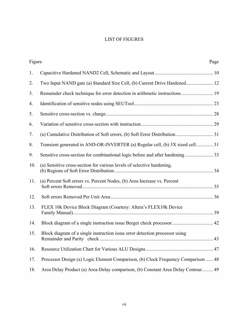
Sensitive cross-section values were also estimated while executing some common ALU
instructions. Sensitive cross-section varies with the instruction executed (Figure 6). Each
instruction exercises a different portion of the logic block, and only those nodes corresponding to
the instruction would be sensitive to a particle strike. Sensitive cross-section also increases with
the increase in the complexity of the function being implemented. For example, the sensitive
cross-section of an ADD combinational block is greater than the sensitive cross-section of an OR
combinational block. The cross-section curves in Figures 5 and Figure 6 are specific to the 4-bit
ALU data path and are also dependent on the mapping effort selected during synthesis.
28
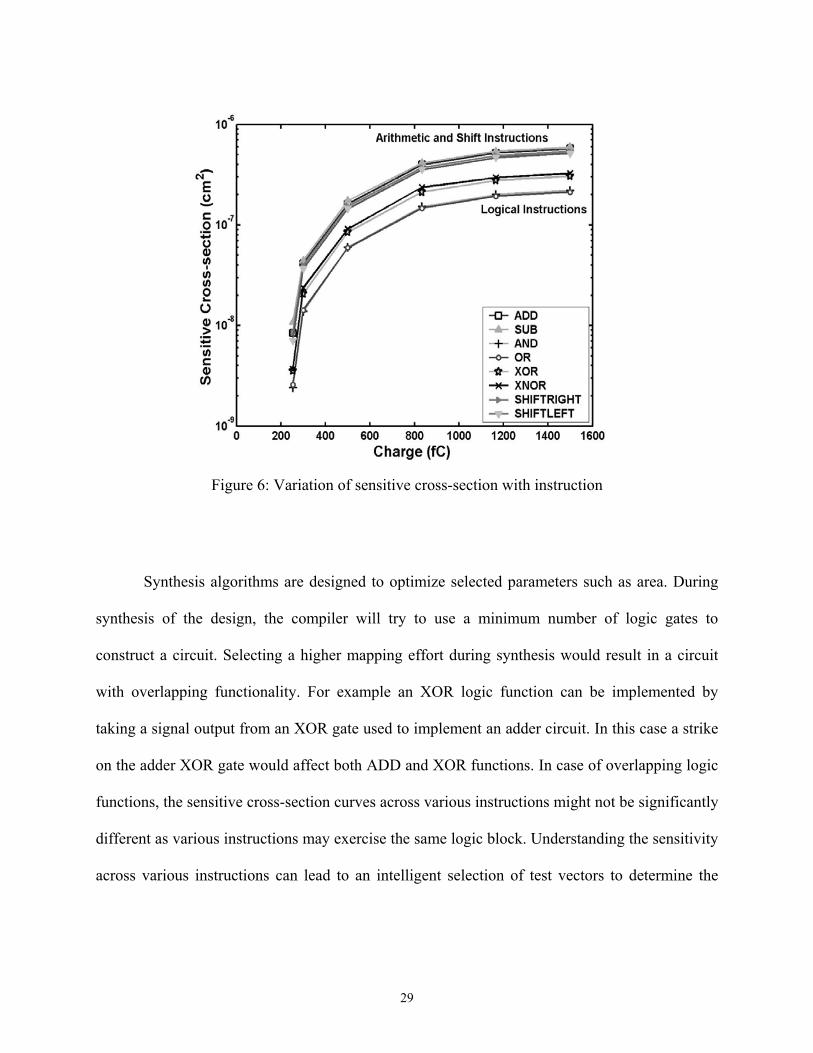
Figure 6: Variation of sensitive cross-section with instruction
Synthesis algorithms are designed to optimize selected parameters such as area. During
synthesis of the design, the compiler will try to use a minimum number of logic gates to
construct a circuit. Selecting a higher mapping effort during synthesis would result in a circuit
with overlapping functionality. For example an XOR logic function can be implemented by
taking a signal output from an XOR gate used to implement an adder circuit. In this case a strike
on the adder XOR gate would affect both ADD and XOR functions. In case of overlapping logic
functions, the sensitive cross-section curves across various instructions might not be significantly
different as various instructions may exercise the same logic block. Understanding the sensitivity
across various instructions can lead to an intelligent selection of test vectors to determine the
29

sensitivity of nodes within the circuit. Such an analysis could effectively reduce the number of
test vectors required to determine sensitive nodes.
(b) Distribution of soft errors
Although there are separate combinational blocks for different functions, the circuit also
has common nodes that would be sensitive across all instructions. Figure 7(a) shows the
cumulative distribution of the soft errors observed for all the nodes in the circuit and Figure 7(b)
shows the soft error histogram for the same circuit. The cumulative distribution of the soft errors
shows that 50% of the nodes contribute to 82% of the soft errors. In this circuit, 50% of the
nodes correspond to an actual node count of 105.
The nodes that contribute the most are likely shared among various instructions. As we
move further along the cumulative distribution curve, we see that the contribution to the total
number of soft errors by each node decreases, and that these nodes are relatively less sensitive.
To get maximum return on resources, the user may choose to harden only those nodes which
contribute to 82% of the soft errors. Because these nodes have a significant contribution to the
total sensitive cross-section, selective hardening of these critical nodes can produce a sensitive
cross-section comparable to hardening all the nodes. The most sensitive 105 combinational logic
nodes were selected from the soft-error distribution.
2) Hardening Sensitive Nodes
A particle strike on a node results in the generation of a voltage transient. The magnitude
of the voltage transient is dependent upon the load capacitance at the node, transistor drive
strength, and the collected charge. This transient could be limited by either increasing the drive
30

Figure 7: (a) Cumulative Distribution of Soft errors, (b) Soft Error Distribution
strength of the sensitive transistors or by increasing the node capacitance [23-25] [52]. Increasing
the capacitance of the node will result in significant speed penalties in addition to the area and
power penalty. Large values of capacitances can also filter out legitimate logic signals in high
frequency circuits. Increasing drive strength could result in area, power and speed penalties, but
the penalties could be optimized by selective hardening.
Figure 8: Transient generated in AND-OR-INVERTER (a) Regular cell, (b) 3X sized cell
31

Both [53] and [54] discuss the impact of a selective hardening strategy with different
transistor sizing on the soft error probability in analog-to-digital converters. Those results show
that for larger values (5pC-10pC) of deposited charge, increasing transistor sizes increases the
soft error sensitivity because now the increase in sensitive drain area dominates the increase in
drive strengths. However, for the 4-bit ALU data path the sensitive cross-section saturates
around 1.5pC and for this charge range results in [53] [54] shows a decrease in sensitivity with
increase in the transistor sizes.
The AND-OR-INVERTER (AOI) is the most sensitive cell in the 105 selected cells. The
AOI cell was simulated in SPICE to determine the transistor sizing for hardening. The drive
strengths of the transistors driving each node were increased until the transient was reduced to
0.5Vdd. The waveforms in Figure 8(a) and Figure 8(b) show the reduction of the transient for the
AOI cell. A 3X increase in size of the AOI cell transistors limits the transient to less than 0.5Vdd.
A worst case sizing factor of 3X is used to eliminate soft errors in all the 105 sensitive nodes. For
smaller cells, a factor less than 3X may be sufficient to limit the transient to 0.5Vdd. However, a
3X increase in size for all the 105 cells would give a worst case impact on the area.
(a) Selective Hardening of Sensitive Nodes by Transistor Sizing
The sensitive cross-section was estimated for the combinational logic by selectively
hardening the most sensitive 105 nodes in the soft error distribution (Figure 9). Because all the
soft errors resulting from the strikes on these nodes are removed, the sensitive areas of those
nodes no longer contribute to the overall cross-section. However, there is still some contribution
from the remaining unhardened 50% of the logic nodes. This results in an order of magnitude
decrease in the sensitive cross-section from selectively hardening 50% of sensitive nodes.
32

Further, the nodes are insensitive up to a deposited charge of 0.6pC. In this case,
additional hardening of combinational logic would not yield any improvement in the total
sensitive cross-section due to the limit posed by the unhardened latches. Traditional hardening
approaches such as DICE latches could be used to further improve the total sensitive cross-
section [55] [56].
Figure 9: Sensitive cross-section for combinational logic before and after hardening
(b) Impact of soft error distribution on SEU Sensitive cross-section
Sensitive cross-section estimates were also obtained by sizing 23% (50 nodes)
and 100% of combinational logic cells (Figure 10(a)) using the above transistor-sizing strategy.
Soft errors corresponding to these nodes are shown in Figure 10(b). As expected, the cross-
33

section of the circuit decreased as more nodes were hardened. To harden the entire circuit, some
of the nodes required more than 3X increase in the device sizes to eliminate transients. The
nodes requiring larger sizing factors were identified. SPICE simulations were performed on each
of these nodes individually and the sizing factors to limit the transient to 0.5Vdd were
determined. Using these sizing factors, the area increase was estimated for hardening selectively
and hardening all the nodes in the circuit.
Figure 10: (a) Sensitive cross-section for various levels of selective hardening, (b) Regions of Soft Error Distribution
3) Area Estimation
Using the cell areas for the logic gates used in the circuit, an area estimate is obtained for
selectively and fully hardening the combinational logic nodes in the 4-bit ALU slice. Figure
11(b) shows the increase in area as a function of percentage of soft errors removed. From Figure
11(a) we can see that 50% of the nodes contribute to 82% of the soft errors. The area of
selectively hardening 50% of the nodes is 1.8 times the unhardened circuit area. Hardening all
the nodes in the circuit by transistor sizing to eliminate the remaining 20% of the soft errors
34

Figure 11: (a) Percent Soft errors vs. Percent Nodes, (b) Area Increase vs. Percent Soft errors Removed
requires 2.97 times the unhardened circuit area, which is also a 65% increase compared to the
selectively hardened circuit. Figure 11(b) is analogous to an area vs. hardness trade-off curve.
As we try to harden more and more nodes, the return on the soft errors removed
diminishes. This is because the nodes in the tail section of the soft error distribution do not
contribute as much to the total soft errors. Further, certain nodes in the tail of the distribution
require greater than 3X increase in size to eliminate the soft errors. This results in an increased
area penalty for hardening nodes in the tail of the distribution. A selectively hardened circuit can
eliminate 82% of the soft errors and it requires only 61% of the area of a fully hardened circuit.
Figure 12 is a chart showing the number of soft errors removed per unit area increase for
hardening various percentages of nodes. Selectively hardening 50% of the nodes remove more
soft errors per unit area increase. For hardening 23% and 100% nodes, number of soft errors
removed per unit area increase is approximately the same. This can be explained by studying
Figure 11 in detail. Figure 11(b) is divided into three regions: (1) Region 1 (0 - 50% soft errors
removed), (2) Region 2 (50% - 82% soft errors removed), and (3) Region 3 (82% - 100% soft
35

Figure 12: Soft errors Removed Per Unit Area
errors removed). A majority of the nodes in Region 1 are AOI cells and multiplexers. Their high
soft error probabilities indicate these cells are likely shared among various instructions.
Even though hardening nodes in the Region 1 eliminates 50% of the soft errors, the area
penalty due to the larger cell area of these nodes reduces the hardening effectiveness. Region 2
consists of 27% of the nodes where a majority of the nodes are inverters. Increasing the size of
inverters would incur a lower area penalty compared to sizing an AOI.
As we harden additional nodes in Region 3, the number of soft errors removed per
hardened cell decreases. Also, some of the cells in Region 3 require larger than a 3X increase in
drive-strength to eliminate soft errors, which further increases the area penalty. The choice is in
the hands of the designer to select between area optimization and radiation hardness. For designs
36

with some flexibility in the radiation hardness requirement, Region 2 offers a balance between
the metrics of area and hardness.
4) Discussion
Both SEUTool and SPICE simulations show that all the nodes in the test circuit are
sensitive for some combination of the input. However, some nodes in the circuit have active
paths to the output more frequently than others. Sensitive cross-section also varies with the
executed instruction. Variation of the sensitive cross-section with the instruction can be used to
determine the sensitive cross-section curve for a given instruction mix to be executed. The
frequency of instructions would influence the total sensitive cross-section. For example, an
instruction mix with many arithmetic instructions would have a greater sensitive cross-section
compared to an instruction mix with large number of logical instructions. The frequency mix of
instructions would determine the sensitive nodes and cross-section of a circuit. Hence, it is
difficult to calculate the absolute sensitive cross-section of a combinational logic circuit. For a
specific application, sensitive nodes can be determined based on the average workload/frequency
of instructions. The cross-section estimated from the average workload would be representative
of the total sensitive cross-section of the circuit. As the sensitivity of a node is dependent on the
application and the work-load, hardening all the nodes in the circuit may not be necessary. Using
average workload, sensitive nodes can be determined and selectively hardened.
So far, we have discussed a soft-error mitigation technique which is applicable for ASIC
logic circuits. Methodology discussed in this chapter is not applicable for FPGAs due to the
architecture of FPGAs. In FPGAs, it is not possible to isolate sensitive nodes; hence a different
37

mitigation technique is necessary. In the next chapter, we would present soft-error mitigation in
FPGAs using Error Detection and Correction Codes.
38

CHAPTER V
PROCESSOR DESIGN FOR SEU MITIGATION IN FPGA BASED LOGIC CIRCUITS
1) Simulation Details
In order to illustrate the EDAC techniques for mitigating soft-errors in FPGAs, a 16-bit
ALU was designed with built-in-error-detection schemes (Berger Check, Remainder and Parity
Check). The ALU can perform basic arithmetic (ADD, SUB and MUL), logical (AND, OR and
Figure 13: FLEX 10k Device Block Diagram (Courtesy: Altera’s FLEX10k Device Family Manual)
39

XOR), shift (SHIFT LEFT and SHIFT RIGHT) and rotate (ROTATE LEFT and ROTATE
RIGHT) operations. The reason for choosing an ALU circuit is because it is representative of a
system level combinational logic circuit. ALUs represent the core of the arithmetic processing
units and a soft-error originating from an ALU can propagate to multiple stages in a processor
pipeline. Further, the difficulty in implementing error detection and correction in ALU makes it
an interesting problem. Arithmetic error correction codes can correct errors in arithmetic
operations, but they are not applicable for logical, shift, and rotate operations [45]. Further, ALU
circuits operate upon the two data symbols applied to its input. The ALU output cannot be
uniquely represented as a combination of inputs. Hence, it is very difficult to implement
linear/block arithmetic codes such as hamming codes, or cyclic codes in ALU circuits [39-41]. In
this chapter, we aim to present an area, performance comparison of two arithmetic codes namely,
Berger Check Prediction, Remainder Check and Parity Check Prediction implementation and a
Triple Mode Redundant Design.
In order to study the BIED techniques, a 16-bit ALU circuit is realized in Altera’s FLEX
10k70RC240 chip as shown in Figure 13. The FLEX 10k70 device consists of 3744 logic
elements which maps to an equivalent gate count of 70000 logic gates. The chip consists of
179/358 I/O pins. The chip is designed in 0.42um CMOS process and uses a 5V supply [57]. For
simulation, the QUARTUS II simulation engine provided by Altera is used [58]. All the ALU
designs were optimized for area. An older version of target device is chosen only to demonstrate
the proof of concept.
40

2) Berger Check Processor Design
In order to demonstrate the Berger check prediction, a single instruction issue processor
with a Berger check ALU is realized in the target device. A single-instruction-issue processor
issues one instruction at a time sequentially. Current processors employ instruction level
parallelism to improve performance. A single-instruction-issue processor design presents the
proof of concept. In Figure 14 (0’s Counter, Berger Check Calculator, Comparator, and DFF)
represent the error detection logic. The error detection logic basically consists of a 0’s counter to
count the number of zeroes in the data symbols X and Y. A multiple-operand carry save adder
(MCSA) performs the Berger check symbol calculation (MCSA implements the table 1
equations). An error signal is generated on mismatch of check symbols. A SEU in the
configuration memory will affect the ALU functionality which in turn may result in a non-
persistent error. This error would be detected by the EDAC circuitry which in turn will generate
an error signal. The error signal can be used to reconfigure the configuration memory. This
would save the cost of scrubbing periodically. Following the scrubbing operation, the instruction
and data can be re-issued in order for the ALU to compute the correct data. However using this
EDAC technique, it is difficult to distinguish between non-persistent data errors and SET data
errors. Both non-persistent and SET data errors would set the error flag; hence the correction
mechanism should be such that it takes care of both error types. As configuration upset induced
errors (such as non-persistent errors) are predominant in FPGAs, one possible correction
mechanism could be to scrub the configuration memory on detection of an error, and re-execute
the instruction, as this would eliminate both types of errors (non-persistent and SET induced data
error).
The following example illustrates the error detection capability of Berger check codes.
41

Example 1: Let X = 101011 and Y = 101101; then N(X) = 4 and N(Y) = 4 or Xc = 2 and Yc = 2.
Let ci = 0, S = X + Y = 011000, and C = 101111. Therefore, N(S) = 2, Sc = 4, N(C) = 5, Cc = 1
and cout = 1. We find N(X) + N(Y) + cin = 4 + 4 + 0 = 8 and N(S) + cout + N(C) = 2 + 1 + 5 = 8,
as described in (5) in Berger check equations. Further, according to (6), Sc = Xc + Yc - Cc - ci +
cout = 2 + 2 - 1 - 0 + 1 = 4. Number of Zeroes in ALU output, S = 4. In case of an SEU in ALU,
no. of zeroes in ALU output and Sc would not match thereby generating an error signal.
StateMachine
Memory
PC
ALU 0’s Counter
Berger Check Calculator 0’s Counter
Comparator
Internal CarriesX
Y
OpcodeCin
Cout
Cout Cin
S
Sc from ALU output
Sc from inputsand carries
Cc
Xc
Yc
DFF
Re
Cl
set
ock
Re-Generate/Re-Configure SignalError_flag_out
16
168
32
BCALU
StateMachine
Memory
PC
StateMachine
Memory
PC
ALU 0’s Counter
Berger Check Calculator 0’s Counter
Comparator
Internal CarriesX
Y
OpcodeCin
Cout
Cout Cin
S
Sc from ALU output
Sc from inputsand carries
Cc
Xc
Yc
DFF
Re
Cl
set
ock
Re-Generate/Re-Configure SignalError_flag_out
16
168
32
BCALU
Figure 14: Block diagram of a single instruction issue Berger check processor
Berger check is optimal for multiple unidirectional error detection. This is because the
check symbol length is minimal for Berger check code among all systematic codes [59] [60].
This means less logic is required to implement Berger check error detection. Further, Berger
check codes scale well with increasing data widths [46] [47]. A larger width Berger check
processor would not require a significant increase in error detection logic.
42

3) Remainder Check And Parity Check Processor Design
Figure 15 shows the error detection processor with the remainder and parity check
scheme. All the blocks except ALU and State Machine represent the error detection circuitry.
Similar to the Berger check prediction processor, the regenerate/reconfigure signal sets the error
flag. The error flag is read during the instruction fetch stage of the processor. If the error flag is
set as high, then the configuration memory is refreshed to eliminate the possibility of a non-
persistent error. The state machine goes into the re-execution stage. The program counter is not
updated and the instruction, data symbols (X, Y) are re-executed. This re-issue of instruction and
data will correct both non-persistent errors as well SET induced data errors. The performance
loss in re-executing instructions would be dependent on the bit error rate (BER) for the circuit. If
the BER is small, then the processor would be running at its normal speed most of the time. Only
during the detection of an error the re-execute state would be carried out.
ALU
Check-Sum/ ParityCalculator
Decoder
Comparator
DFF
StateMachine
Memory
PC
Reset
32
16
8
Data OpcodeALU output
ck
Enable
Re-Generate/Re-Configure SignalError_flag
Clo
ALU
Remainder / ParityCheck from inputs
Remainder / Parity Check from ALU output
Comparator
DFF
StateMachine
Memory
PC
16
EDALU
ALU
Check-Sum/ ParityCalculator
Decoder
Comparator
DFF
StateMachine
Memory
PC
ALU
Check-Sum/ ParityCalculator
Decoder
Comparator
DFF
StateMachine
Memory
PC
StateMachine
Memory
PC
Reset
32
16
8
Data OpcodeALU output
ck
Enable
Re-Generate/Re-Configure SignalError_flag
Clo
ALU
Remainder / ParityCheck from inputs
Remainder / Parity Check from ALU output
Comparator
DFF
StateMachine
Memory
PC
StateMachine
Memory
PC
16
EDALU
Figure 15: Block diagram of a single instruction issue error detection processor using remainder/parity check
43

In the Berger check processor, the error detection circuitry will always be sensitive. In the
Remainder and Parity Check processor, the error detection (ED) circuitry is separated for various
instructions (Figure 15). A strike on the shift instruction parity logic would not have any effect
on the output while executing arithmetic, logical, or rotate instructions. The processor
performance penalty and sensitivity would depend upon the application run by the processor. For
example, a SEU on the configuration logic may affect the logical instructions. However, if the
application run on the processor consists of a series of arithmetic instructions, then the SEU
would not have any effect on the ALU output. The processor would go into the re-execute stage
only when a logical instruction is executed. The performance penalty is minimized by re-
configuring the circuit on-demand, when the error is detected. The performance penalty can be
tested by running some benchmark applications.
(a) Choice of Check Divisor
The main drawback of remainder check technique is the need to calculate the remainder
multiple times. Array dividers are fast but have prohibitive area requirements. For efficient and
widespread use of this technique, a fast remainder calculation circuit is required which uses
significantly less area overhead.
Generating remainder checks using (Base – 1) as the check divisor greatly reduces the
amount of logic required for implementing error detection. (Base – 1) division is similar to
remainder from dividing by 9. For, example remainder of 44 divided by 9 can be calculated by
simply adding the individual digits in the dividend (4 + 4) = 8 (also known as “Proof by 9”). This
methodology is application for division under any base. The advantage of this coding scheme is
due to the fact that, a series of adder circuits can be used to implement remainder check. For
44

example, a 16-bit ALU would require six 4-bit ADD operations to generate the remainders for
the ALU input data symbols. This method not only minimizes the area of error detection logic,
but also reduces the delay involved in calculation of remainder check codes. The remainder
check codes are computed in parallel with the ALU operations. Proper timing will ensure that the
check codes for input data and output data are available for comparison at the same clock cycle
for low overhead. Following example illustrates the use of (Base – 1) as check divisor to
simplify the remainder check codes.
Example 2: X = 0x1EF2, Y = 0x0324, where X and Y represent the hexadecimal representation
of data symbols X and Y. The remainder calculation can be quite complex and may increase the
area of the error detection logic. Proper choice of check divisor can simplify the calculation of
the remainder. The remainder check is analogous to a CRC; it only serves the purpose of
generating remainder for error detection. The choice of the check divisor would not have any
effect on the error detection principle. In base “A” arithmetic, choosing “(A-1)” as the check
divisor simplifies the remainder calculation problem.
For base 16 (hexadecimal) arithmetic, 2m = 1610, and the check divisor P = A – 1 = (2m –
1) = 1510 (i.e., F16). For the check divisor P = F16, the remainder can be readily calculated by
adding the individual hexadecimal digits of X and Y. For the above example, RX = (1EF2)16 / F16
= (1 + E + F + 2)16 = 2016. As this answer is greater than the base, one more add operation is
needed to yield RX = (20)16 / F16 = (2 + 0)16 = 216. Similarly, RY = (0324)16 / F16 = (0 + 3 + 2 +
4)16 = 916. As this number is less than the base, no further add operations are required. For the
remainder check code, RCCin = (RX + RY) / P = (2 + 9)16 / F16 = B16. The ALU output is given by S
= X + Y = (1EF2 + 0324)16 = 221616. Then, RCCout = (2216)16 / F16 = (2 + 2 + 1 + 6)16 = B16. In
case of an error, RCCin and RCCout would not match, thereby generating an error signal. The
45

algorithm presented in this section simplifies the division operation into series of add operations
which significantly reduces the logic required for error detection.
46

CHAPTER VI
IMPACT OF SEU MITIGATON ON AN FPGA-BASED ALU
1) Simulation Results
The ALU designs were simulated using Quartus II Version 5.0 simulation tool
provided by Altera. The FPGA resource utilization of the two BIED techniques (Berger Check,
Remainder and Parity Check) was recorded from the simulation. Figure 15 shows the resource
utilization comparison chart for the two BIED techniques compared with a TMR ALU and an
ALU without any error detection.
TMR - TRIPLE MODE REDUNDANCY BC - BERGER CHECK ED - REMAINDER/PARITY CHECK
Figure 16: Resource Utilization Chart for Various ALU Designs
47

Figure 17: Processor Design (a) Logic Element Comparison, (b) Clock Frequency Comparison
We can see from Figure 16 that EDALU (ALU with remainder and parity check) uses
46% of the logic elements compared to the TMR ALU, and the Berger check prediction ALU
uses 58% of the logic elements compared to a TMR ALU. However, the TMR ALU is capable of
correcting single bit non-persistent and SET data errors, whereas BCALU and EDALU can only
detect errors. The error correction is achieved by refreshing the configuration memory, followed
by re-executing the instruction and data. There would be a performance penalty associated with
re-execution of instruction. This performance penalty would be determined by the frequency of
errors.
Our goal here was to find a technique that would detect and correct soft errors in a FPGA
circuit without incurring the 3X penalty of a TMR technique. The resource utilization chart
shows that the error can be detected by incurring less than 2X area penalty. Figure 17(a) and
17(b) are the area and performance comparison chart of a single instruction issue processor
designed using the three versions of the ALU. The Berger check processor uses 60% of the area
of the TMR processor, but runs at 85% of its clock frequency, whereas the EDALU (Remainder
and Parity check) uses 49% of logic elements and runs at 60% of the clock frequency of TMR
48

Values normalized to TMR processor
TMR - TRIPLE MODE REDUNDANCYBC - BERGER CHECKED - REMAINDER/PARITY CHECK ` TMR Processor
ED Processor
BC Processor
Values normalized to TMR processor
TMR - TRIPLE MODE REDUNDANCYBC - BERGER CHECKED - REMAINDER/PARITY CHECK
Values normalized to TMR processorValues normalized to TMR processor
TMR - TRIPLE MODE REDUNDANCYBC - BERGER CHECKED - REMAINDER/PARITY CHECK ` TMR Processor
ED Processor
BC Processor
` TMR Processor
ED Processor
BC Processor
Figure 18: Area Delay Product (a) Area-Delay comparison, (b) Constant Area Delay Contour
processor. The performance of the EDALU is affected by the sequential decoding element in the
error detection circuitry. In the Berger check processor, the decoder is just a 0’s counter, whereas
in an EDALU processor the decoder circuitry consists of remainder and parity calculation logic.
The remainder calculation block consists of a series of adders which introduces some delay into
the circuit. The choice between EDALU and BCALU is user dependent. If the designer wants to
optimize for area while eliminating single-bit errors, then the EDALU would be the right choice,
whereas, if the performance of system needs to be optimized, then the BCALU is a better choice.
Further the BCALU scales well, and the area efficiency would increase with an increase in data
width. The BCALU can also detect multiple feed-forward logic errors. A combination of the
Berger check and EDALU can also be developed to optimize on the area/performance metrics.
Figure 18(a) shows the area-delay product chart for the three ALU processors. Both the
Berger check and the remainder and parity check processors have a smaller area-delay product
when compared to the TMR ALU. The area penalty of both the BIED designs is less than 2X,
which means BIED techniques are efficient compared to dual mode redundancy for error
detection. Further, dual mode redundancy for error detection does not scale well with increasing
49

data size. Figure 18(b) shows the constant area delay contour for the implementation of the three
ALUs in a single-instruction-issue processor. As we move in the direction of the arrow, the area
and the delay penalty reduces. Based on the resource allocation restrictions, the user can choose
between different techniques. For example with 3500 logic elements, the designer can choose
TMR ALU due to its ease of implementation and minimum performance penalty. For smaller
logic element resource, the user may choose between the Berger check and the EDALU based on
the bit error rate and the number of soft errors to be eliminated.
Reissuing the instruction and data would affect the system performance. However, it is
dependent on the frequency of occurrence of errors. For lower error rates [61], the resource
utilization of a TMR based processor would be inefficient. With a slight compromise in
performance by re-executing the instruction, the errors can be eliminated at the instant of
detection. Furthermore, for non-persistent data errors, the scrubbing can be done on demand
when the error is detected. However, cost-benefit of scrubbing on demand over scrubbing
periodically must be determined.
2) Discussion
TMR and scrubbing to correct bit stream errors involve penalties. Furthermore, only 45%
of the total errors observed in FPGAs account for configuration bit-stream errors (non-persistent
data errors) [61]. Redundancy techniques to mitigate SET and non-persistent data errors would
involve huge area and power penalties. Built-In-Error-Detection techniques can be used to detect
errors in data bits as well as configuration bits.
For lower error rates, the resource utilization of TMR would be highly inefficient.
Instead, errors can be detected by using BIED techniques and error correction can be applied
50
once an error is detected. Among the three different schemes studied, Berger check error
detection minimizes the penalties and also scales well as we move to larger bit size. The area-
delay product of a Berger check processor is 70% of the TMR processor.
51

CHAPTER VII
CONCLUSION
Traditional soft error mitigation techniques for both ASIC-based and FPGA-based logic
circuits improve reliability by targeting the whole design. Techniques like Triple Mode
Redundancy (TMR), temporal sampling, scrubbing, and reconfiguration involve significant
penalties (sometimes greater than 3X). In commercial and non-critical applications, significant
area, performance, and power penalties cannot be tolerated. Further, most of the commercial and
non-critical applications may not require a fully hardened implementation. ASIC and FPGA
logic designers should have the flexibility to optimize the trade-off between reliability
requirements and the associated penalties.
This thesis presents alternative soft error mitigation techniques for ASIC-based and
FPGA-based logic circuits. In the ASIC implementation, a 4-bit ALU design is analyzed using
VHDL logic simulations and circuit-level SPICE simulations to determine the sensitive nodes.
The nodes are ranked in the order of their sensitivity. Based upon the rank distribution, 50% of
the most sensitive nodes are selectively hardened by increasing transistor drive strengths. Results
show that selective hardening strategies clearly have a distinct advantage over hardening the
complete circuit. The methodology, when applied on a 4-bit ALU test circuit, results in a circuit
which uses 61% of the area of a fully hardened circuit while providing a comparable level of
radiation hardness. Further, a selectively hardened ALU circuit mitigates 82% of the soft errors
with an area penalty of 1.82X.
52

In the FPGA implementation, a single instruction issue processor is designed
using various error detection and correction schemes (EDAC). A global EDAC technique based
on a Berger check code implementation and an instruction group EDAC technique based on
Remainder and Parity Check design are compared against a TMR design. A comparison of area
and performance results from the three processor implementations shows that Berger check
prediction minimizes penalties and also scales well with larger data bit size. The area-delay
product of a Berger check processor is 70% of the TMR processor. Even though a TMR design
would eliminate all errors due to configuration upsets and SETs, the resource utilization of a
TMR circuit would be highly inefficient for a non-critical application. Hence, by using EDAC
techniques, reliability and performance can be slightly traded for significant improvement in
area.
The analysis performed on an ALU implemented as an ASIC logic as well as an
FPGA design demonstrates the applicability of alternative soft error mitigation techniques such
as transistor sizing or EDAC codes. However, the improvement in area, power, or performance
can be achieved only by trading-off reliability. Hence, it is up to a designer to make the decision
based on application, reliability requirements, and cost-performance metrics.
53

REFERENCES
[1] L. Lantz II, “Soft errors induced by alpha particles,” IEEE Transactions on Reliability., vol.
45, pp. 174–179, June 1996. [2] The National Technology Roadmap for Semiconductors. San Jose, CA: Semiconductor
Industry Association, 2000. [3] C.S. Guenzer, E.A. Wolicki, and R.G. Allas, “Single Event Upset Of Dynamic RAMS By
Neutrons And Protons,” in Proc. IEEE Transactions on Nuclear Science, NS-26, (6), 5048, (1979).
[4] C.S. Guenzer, A.B. Campbell, and P. Shapiro, “Single Event Upsets In NMOS
Microprocessors,” in Proc. IEEE Transactions on Nuclear Science, NS-28, (6), 3955, (1981).
[5] R. Katz, J.J. Wang, K.A. LaBel, J. McCollum, R. Brown, B. Cronquist, S. Crain, T. Scott,
W. Paolini, and B. Sin “Current Radiation Issues For Programmable Elements And Devices,” in Proc. IEEE Transactions on Nuclear Science, NS-45, 2600, (1998).
[6] J. Wang, et-al, “SRAM Based Reprogrammable FPGA For Space Applications,” in Proc.
IEEE Transactions on Nuclear Science, 1999, Vol. 46, No. 6, December 1999, page 1728. [7] S. Buchner, M. Baze, D. Brown, D. McMorrow, and J. Melinger, “Comparison Of Error
Rates In Combinational And Sequential Logic,” IEEE Transactions on Nuclear Science, 44(6):2209–2216, December 1997.
[8] N. Seifert, et al., “Frequency Dependence Of Soft Error Rates For Sub-Micron CMOS
Technologies,” In Proc. Electron Devices Meeting, 2001, IEDM Technical Digest. International, 2-5 Dec. 2001, pp. 14.4.1 - 14.4.4.
[9] J. A. Fifield and C. H. Stapper, “High-speed On-Chip ECC For Synergistic Fault-Tolerant
Memory Chips,” in Proc. IEEE Journal of Solid-State Circuits, vol. 26, no. 10, pp. 1449–1452, Oct. 1991.
[10] D. Yu-Lam, J. Lan, L. McMurchie and C. Sechen, “SEE-Hardened-By-Design Area-
Efficient SRAMs,” In the Proceedings of IEEE Aerospace Conference, pp. 1-7, March 2005.
[11] Neeraj Kaul, “Computer Aided Estimation Of Vulnerability Of CMOS VLSI Circuits To
Single-Event Upsets,” Doctor of Philosophy Dissertation, Vanderbilt University, August 1992.
54

[12] N. Cohen, T.S. Sriram, N. Leland, D. Moyer, S. Butler and R. Flatley, “Soft Error
Considerations For Deep-Submicron CMOS Circuit Applications,” Intl. Electron Devices Meeting Technical Digest, pp. 315-318, 1999.
[13] R. W. Keyes, “Fundamental Limits Of Silicon Technology,” Proc. IEEE, vol. 89, no. 3, pp.
227–339, Mar. 2001. [14] D. G. Mavis and P. H. Eaton, “Soft Error Rate Mitigation Techniques For Modern
Microcircuits,” Proc. Intl. Reliability Physics Symposium, pp. 216-225, 2002. [15] P. Shivakumar, M. Kistler, S. W. Keckler, D. Burger and L. Alvisi, “Modeling The Effect
Of Technology Trends On The Soft Error Rate Of Combinational Logic,” Proc. Intl. Conference on Dependable Systems and Networks, pp. 389-398, 2002.
[16] Murli Dharan Satagopan, “Evaluation Of Single Event Vulnerability For Complex Digital
Circuits,” Master of Science Thesis, Vanderbilt University, August 1994. [17] L.W. Massengill, M. S. Reza, B. L. Bhuva, and T. L. Turflinger, “Single Event Upset
Cross-Section Modeling In Combinational CMOS Logic Circuits,” Journal of Radiation Effects, Research, and Engineering, vol. 16, no. 1, 1998.
[18] L. W. Massengill, A. E. Baranski, D. O. Van Nort, J. Meng and B. L. Bhuva, “Analysis Of
Single-Event Effects In Combinational Logic – Simulation Of The AM2901 Bitslice Processor,” IEEE Trans. on Nuclear Science, vol. 47, No. 6, pp. 2609–2615, December 2000.
[19] Quming Zhou, Kartik Mohanram, “Cost-Effective Radiation Hardening Technique For
Combinational Logic,” Intl. Conference on Computer-Aided Design, 2004. [20] K. Mohanram and N. A. Touba, “Cost-Effective Approach For Reducing Soft Error Failure
Rate In Logic Circuits,” in Proc. Int. Test Conf. (ITC), 2003, pp. 893–901. [21] M. Nicolaidis, “Time Redundancy Based Soft-Error Tolerance To Rescue Nanometer
Technologies,” In Proc. VTS 99. [22] L. Anghel, D. Alexandrescu and M. Nicolaidis, “Evaluation Of A Soft-Error Tolerance
Technique Based On Time And/Or Space Redundancy,” In the Proceedings of the 13th Symposium on Integrated Circuits and Systems Design, pages 237 – 242, 2000.
[23] Stephen P. Buchner and Mark P. Baze, “Single-Event Transients In Fast Electronic
Circuits,” Section V 2001 IEEE NSREC short course, July 16, 2001 Vancouver Canada. [24] M. P. Baze, J. C. Killens, R. A. Paup and W. P. Snapp, “SEU Hardening Techniques For
Retargetable, Scalable, Sub-Micron Digital Circuits And Libraries,” Single Event Effects Symposium Proceedings, 2002.
55

[25] Q. Zhou and K. Mohanram, “Transistor Sizing For Radiation Hardening,” In the
Proceedings of Intl. Reliability Physics Symposium, pp. 310-315, 2004. [26] Carl Carmichael, Michael Caffrey, and Anthony Salazar, “Correcting Single-Event Upsets
Through Virtex Partial Configuration,” Xilinx Application Notes 216, v1.0. Xilinx, Inc., June 2000.
[27] Carl Carmichael, “Triple Module Redundancy Design Techniques For Virtex FPGAs,”
Technical report, Xilinx Corporation, November 1, 2001.XAPP197 (v1.0). [28] Nathan Rollins, Michael Wirthlin, Paul Graham, and Michael Caffrey, “Evaluating TMR
Techniques In The Presence Of Single Event Upsets,” In the proceedings of Annual International Conference on Military and Aerospace Programmable Logic Devices, May 2003.
[29] Nathan Rollins and Michael Wirthlin, “Effects Of TMR On Power In An FPGA,” In the
proceedings of Military and Aerospace in Programmable Logic Devices, Washington DC, September 2004.
[30] J. Gaisler, “A Portable And Fault-Tolerant Microprocessor Based On The SPARC V8
Architecture,” In the Proceedings of the International Conference on Dependable Systems and Networks, pages 409-415, 2002.
[31] Gaisler Research, http://www.gaisler.com. [32] D. E. Johnson et al., “Persistent Errors In SRAM Based FPGAs,” In the proceedings of
Military and Aerospace in Programmable Logic Devices, Washington DC, September 2004.
[33] S.E. Diehl-Nagle, J.E. Vinson, and E.L. Petersen, “Single Event Upset Rate Predictions for
Complex Logic Systems,” IEEE Transactions on Nuclear Science, NS-31, 1132 (1984). [34] John P. Uyemura, “CMOS Logic Circuit Design,” Kluwer Academic Publishers, ISBN 0-
7923-8452-0, 1999. [35] MOSIS, http://www.mosis.org/Technical/Testdata/tsmc-018-prm.html [36] R. C. Baumann, “Single-Event Effects In Advanced CMOS Technology,” in Proc. IEEE
Nuclear and Space Radiation Effects Conf. Short Course Text, 2005. [37] J. Barth, “Modeling Space Radiation Environments” IEEE NSREC Short Course, Session I,
page 54, July ’97, Snowmass, Colorado. [38] William F. Heidergott, “System Level Mitigation Strategies,” IEEE NSREC Short Course,
Session V, pp. 40-46, July 1999, Norfolk, Virginia.
56

[39] Shu Lin and Daniel J. Costello, Jr., “Error Control Coding – Fundamentals and
Applications”, Prentice-Hall, (1983). [40] Eiji Fujiwara and Dhiraj K. Pradhan, “Error-Control Coding in Computers”, Computer,
(July 1990). [41] H. L. Garner, “Error Codes For Arithmetic Operations,” IEEE Transactions on Electronic
Computers (EC-15), pp. 763-770, October 1966. [42] Nirmal R. Saxena, Chih-Wei David Cahng, Kevin Dawallu, Jaspal Kohli, and Patrick
Helland, “Fault-Tolerant Features in the HaL Memory Management Unit”, IEEE Transactions on Computers, pp170-180, (February 1995).
[43] A. D. Anderson, “Design Of Self-Checking Digital Networks Using Coding Techniques,”
Coordinates Sciences Laboratory, Report R/527, University of Illinois, Urbana, September 1971.
[44] R. W. Hamming, “Error Detecting And Error Correcting Codes,” Bell Systems Tech.
Journal, pp. 147-160, 1950. [45] M. Nicolaidis, “Efficient Implementations Of Self-Checking Adders And ALUs,” in Proc.
of Int. Symp. Fault-Tolerant Computing, pp. 586 - 595, 1993. [46] J. C. Lo et al., “An SFS Berger Check Prediction ALU And Its Application To Self
Checking Processor Designs,” IEEE Trans. on Computer Aided-Design, vol. 11, pp. 525-540, Apr. 1992.
[47] J. C. Lo et al., “Concurrent Error Detection In Arithmetic And Logical Operations Using
Berger Codes,” Proceedings of 9th Symposium on computer arithmetic, pp. 233 -240, Sep 1989.
[48] P. Liden, P. Dahlgren, R. Johansson and J. Karlsson, “On Latching Probability Of Particle
Induced Transients In Combinational Networks,” In the Proceedings of the 24th Symposium on Fault-Tolerant Computing (FTCS-24), pages 340–349, 1994.
[49] N. Seifert, X. Zhu, D. Moyer, R. Mueller, R. Hokinson, N. Leland, M. Shade and L.
Massengill, “Frequency Dependence Of Soft Error Rates For Deep Sub-Micron CMOS Technologies,” IEDM technical digest p. 14.4.1, 2001.
[50] L. W. Massengill, “SEU Modeling And Prediction Techniques,” IEEE NSREC Short
Course, Snowbird, Utah, 1993. [51] J. Grad, J. E. Stine, “A Standard Cell Library For Student Projects,” International
Conference on Microelectronic Systems Education, IEEE Computer Society, pp. 98-99, 2003.
57

[52] H. Cha, E. M. Rudnick, J. H. Patel, R. K. Iyer and G. S. Choi, “A Logic Level Model For
α–Particle Hits In CMOS Circuits,” In the proceedings of IEEE international conference on computer design, Oct 1993, pp. 538-542.
[53] M. Singh and I. Koren, “Fault-Sensitivity Analysis And Reliability Enhancement Of
Analog-To-Digital Converters,” In IEEE Transactions on Very Large Scale Integration Systems, vol. 11, pp. 839-852, 2003.
[54] M. Singh and I. Koren, “Reliability Enhancement Of Analog To Digital Converters
(ADCs),” In IEEE Intl. Symp. on Defect and Fault Tolerance in VLSI Systems, Oct. 2001. [55] T. Calin et. al, “Upset Hardened Memory Design For Submicron CMOS Technology”,
“IEEE Transactions on Nuclear Science”, vol. 43, No.6, December 1996, pp.2874-2878. [56] T. Monnier, F. M. Roche and G. Cathebras, “Flip-Flop Hardening For Space Applications,”
In the proceedings of the Intl. Workshop on Memory Technology Design and Testing, pp. 104-107 , August 1998.
[57] FLEX, http://www.altera.com/literature/dp/flex10k/epf10k70.pdf [58] Quartus 5.1, http://www.altera.com/support/licensing/lic-index.html [59] C. Metra et. al, “Novel Berger Code Checker,” IEEE Proceedings on Defect and Fault
tolerance in VLSI systems, Nov. 1995, pp. 287-295. [60] C. V. Frieman, “Optimal Error Detection Codes For Completely Asymmetric Binary
Channels,” Inform. Contr., vol. 5, pp. 64 - 71, March 1962. [61] Earl Fuller, Michael Caffrey, Carl Carmichael, Anthony Salazar and Joe Fabula, “Radiation
Testing Update, SEU Mitigation, and Availability Analysis of the Virtex FPGA for Space Reconfigurable Computing,” In the proceedings of military applications in programmable logic devices, Laurel, Maryland, September 2000.
58


![ASIC Design & FPGA-1st Chapter[1]](https://img.pdfslide.us/doc/110x75/577d203f1a28ab4e1e925961/asic-design-fpga-1st-chapter1.jpg)