Embed Size (px)
Citation preview
Microprocessors and Microsystems xxx (2012) xxx–xxx
Contents lists available at SciVerse ScienceDirect
Microprocessors and Microsystems
journal homepage: www.elsevier .com/locate /micpro
FPGA-based implementation alternatives for the inner loop of the Secure HashAlgorithm SHA-256
I. Algredo-Badillo a, C. Feregrino-Uribe b, R. Cumplido b,⇑, M. Morales-Sandoval c
a Computer Engineering, University of Istmo, Tehuantepec, Oaxaca 70760, Mexicob National Institute for Astrophysics, Optics and Electronics, Santa. Ma. Tonantzintla, Puebla 72840, Mexicoc Polytechnic University of Victoria, Information Technology Department, Tamaulipas 87138, Mexico
a r t i c l e i n f o a b s t r a c t
Article history:Available online xxxx
Keywords:SHA-2Hash functionFPGA
0141-9331/$ - see front matter � 2012 Elsevier B.V. Ahttp://dx.doi.org/10.1016/j.micpro.2012.06.007
⇑ Corresponding author. Tel.: +52 222 2663100x82E-mail addresses: [email protected]
[email protected] (C. Feregrino-Uribe), [email protected] (M. Morales-Sandoval).
Please cite this article in press as: I. Algredo-Bad256, Microprocess. Microsyst. (2012), http://dx.
Hash function algorithms are widely used to provide security services of integrity and authentication,being SHA-2 the latest set of hash algorithms standardized by the US Federal Government. The main com-putation block in SHA-2 algorithms is governed by a loop with high data dependence for which severalimplementation strategies are explored in this work as well as designs efficiently mapped to hardwarearchitectures. Four new different hardware architectures are proposed to improve the performance ofSHA-256 algorithms, reducing the critical path by reordering some operations required at each iterationof the algorithm and computing some values in advance, as possible as data dependence allows. The pro-posed designs were implemented and validated in the FPGA Virtex-2 XC2VP-7. The achieved results showa significant improvement on the performance of the SHA-256 algorithm compared to similar previouslyproposed approaches, obtaining a throughput of 909 Mbps and an improved efficiency of 0.713 Mbps/slice.
� 2012 Elsevier B.V. All rights reserved.
1. Introduction algorithms [2,3]. Several algorithms for performing hash functions
Digital communication systems are widely used for executing awide variety of electronic operations such as: electronic transfers,mobile communications, multimedia, electronic commerce, docu-ment transfers, and videoconferences, among others. The informa-tion being transmitted by these systems can potentially be at risk ifno security measures are taken. The most common risks found inthese systems include: non-authorized accesses, denial of service,data corruption, leakage, monitoring attacks, authentication, andtrashing [1]. Several measures can be taken to reduce such risks;among the most common are the use of firewalls, traffic filtering,and detection systems. Additionally, security can also be providedby using cryptographic algorithms [1].
Hash functions are cryptographic primitives widely used to pro-vide services of data integrity and authentication issues. Thesefunctions allow to maintain a high level of security by performingcomplex operations, usually in an iterative fashion, which require asignificant amount of computing resources. A hash function mapsbinary strings of arbitrary length to binary strings of some fixedlength, called hash-value or digest. Hash functions are widelyspread and mainly used for the implementation of digital signature
ll rights reserved.
25; fax: +52 222 2663152.o.edu.mx (I. Algredo-Badillo),
[email protected] (R. Cumplido),
illo et al., FPGA-based implemedoi.org/10.1016/j.micpro.2012.
[1] have been proposed: MD5, SHA-1, SHA-2, Whirlpool, Haval, andRipeMD-160, being the SHA family the most widely used, in partic-ular SHA-2 that offers higher security and solved the insecurityproblems of SHA-1 [4] and other popular algorithms as MD5 andSHA-0 [5,6] (already broken). Currently, several hash function algo-rithms are being evaluated to select SHA-3 [7,8].
The efficient implementation of hash functions has been an ac-tive research topic in industry and academia in recent years. Thereare several research papers and commercial products that offerhardware or software implementations of one or more algorithmsfrom the SHA-2 family. The hardware architectures previously re-ported aim to achieve better performance by customizing hard-ware elements that efficiently compute specific functions. Maintechniques previously used include the use of well balanced CarrySave Adders (CSA) [9], unrolling techniques [10,11], the usage ofembedded memories [12], the use of pipelining techniques [13]among others. In general, these techniques resulted in more arearequirements or more complex control logic that affect the criticalpath and decrease the performance. This work describes two strat-egies to improve the performance of hardware implementation ofthe main operations in the SHA-2 algorithms. The critical path isreduced by predicting the result of some computations in the innerloop of SHA-2 algorithms up to two operations in advance. Thecritical path is also decreased by reducing latency of the calcula-tions by re-arranging operations in the core of SHA-2 algorithms.The architectures proposed in this work are optimized to execute
ntation alternatives for the inner loop of the Secure Hash Algorithm SHA-06.007
2 I. Algredo-Badillo et al. / Microprocessors and Microsystems xxx (2012) xxx–xxx
the entire algorithm of hashing, not only for processing a singleblock as in [13]. The four proposed architectures use carry save ad-ders (CSAs), balancing of datapaths, and a 256-bit state buffer tostore the eight registers A � H to compute the hashing. This statebuffer is considered as a single signal that is feed backed to processeach new data block. In [13], feed backing process is based on theuse of multiplexers and single 32-bit registers but that approachmay result in larger data paths and more complex control logicthat could increase the delay of the critical path and decrease theperformance. The proposed hardware designs were evaluated forthe SHA-256 algorithm implemented on the Virtex-2 XC2VP-7FPGA device. However, these designs can be easily extended forother hash algorithms in the SHA-2 family, which present a com-mon structure. Compared to similar approaches such as [13], thethroughput per slice efficiency achieved in this work is the highest,reaching around 909 Mbps with an area usage of 1150 FPGA slices.The work presented here is an extended version of [14], where twohardware architectures for computing the inner loop of SHA-2algorithms were reported. The main idea in [14] is the computationof some additions in the inner loop one iteration in advance to re-duce the critical path delay in the next iteration. While the firstarchitecture is based in the use of a subtraction, the second oneis only based on precomputed additions. In the present work, CarrySave Adders are used to perform the additions demanded in the in-ner loop of SHA-2 algorithms instead of traditional adders, whichallows to reduce the critical path delay. In addition, a new evalua-tion platform is designed to execute the entire SHA-2 algorithm,where the datapath is shortened by adding 2 new registers withoutincreasing the latency. This platform allows to evaluate the twohardware proposals for the inner loop, executing the entire SHA-2 algorithm and achieving improved results compared to the onesreported in [14].
The rest of this paper is organized as follows: Section 2 de-scribes the SHA-2 family, Section 3 shows the details of datadependence in SHA-256 algorithm, Section 4 presents the pro-posed architectures for computing the main operations of SHA-2,Section 5 describes the implementation details and discusses theresults, and finally Section 6 concludes.
64 Iterations
Message Block
B
Initial Hash Value
H0512256
32
32
A B C D E F G H
256
tt
2. Secure Hash Algorithms
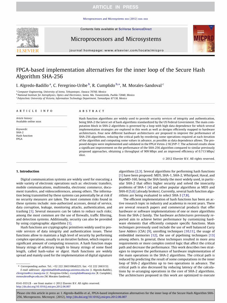
Hash functions are mainly used to provide the security serviceof integrity. They also provide the security service of authentica-tion when they are used in combination with digital signatureand message authentication code (MAC) algorithms. Among themost important hash functions is the SHA-2 family, which sharethe same functional structure with some variation in the internaloperations, message size, message block size, word size, numberof security bits and message hash size, see Table 1 [15].
These algorithms are iterative and one-way functions that inputa message and output a message digest. They process the inputdata in two stages: preprocessing and digest computing. The pre-processing warranties that the message has a size that is multipleof a particular value, allowing to divide the message into prede-fined block sizes and to provide an initial hash value. In the second
Table 1Secure Hash Algorithms (sizes and security are specified in bits).
Algorithm SHA-1 SHA-256 SHA-384 SHA-512
Message size <264 <264 <2128 <2128
Block size 512 512 1024 1024Word size 32 32 64 64Message digest size 160 256 384 512Security 80 128 192 256
Please cite this article in press as: I. Algredo-Badillo et al., FPGA-based implem256, Microprocess. Microsyst. (2012), http://dx.doi.org/10.1016/j.micpro.2012.
stage, each message block is utilized during a fixed number of iter-ations, where at each iteration the algorithm defines functions,constants and word operations to generate a series of hash values.After all blocks are processed, the value of the final hash is used asthe message digest. In particular, the second stage of the SHA-256algorithm performs 64 iterations over blocks of 512-bit messagesand hash values of 256 bits described as eight 32-bit words(A,B, . . . ,H). The hash message is 256-bit long, see Fig. 1.
3. Related works
Implementations of hash functions require great amounts ofspatial and temporal resources that may result in low performanceand efficiency. This has motivated the research on several ap-proaches for speeding up the computation or for improving theefficiency in terms of throughput/area ratio.
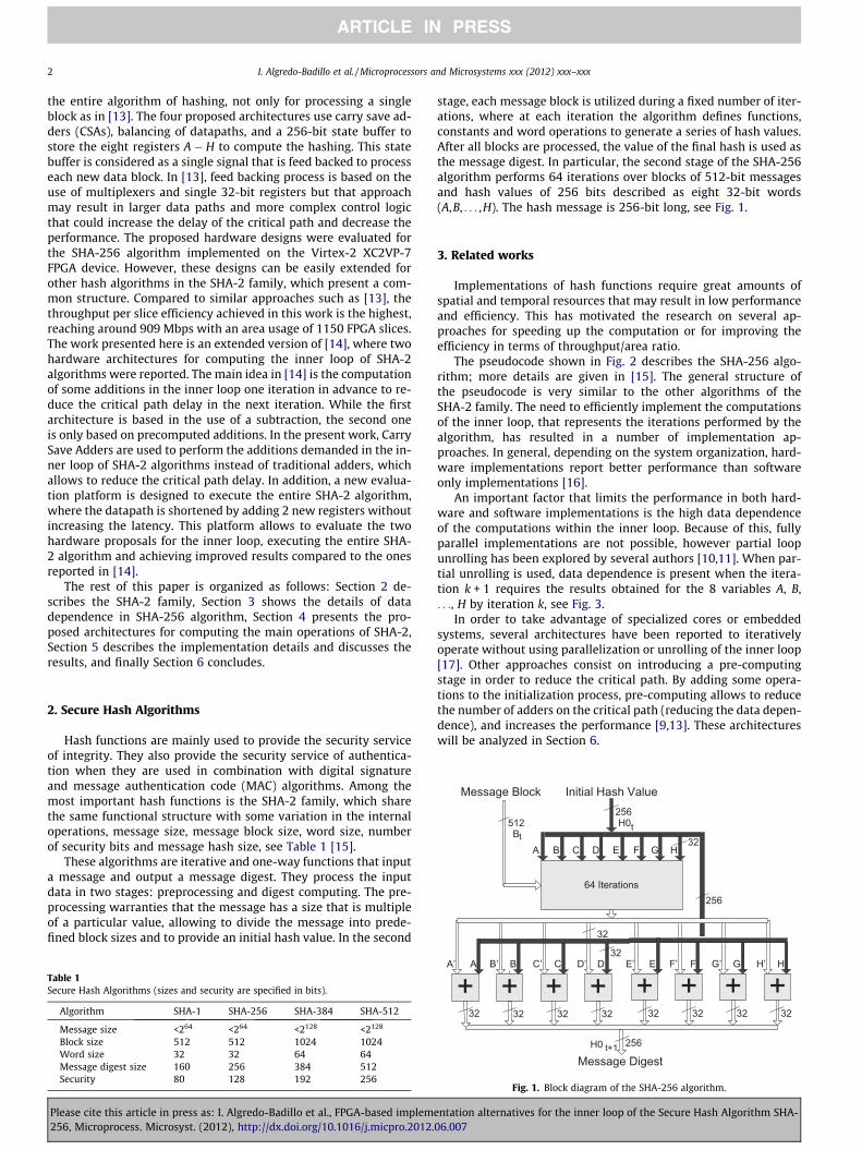
The pseudocode shown in Fig. 2 describes the SHA-256 algo-rithm; more details are given in [15]. The general structure ofthe pseudocode is very similar to the other algorithms of theSHA-2 family. The need to efficiently implement the computationsof the inner loop, that represents the iterations performed by thealgorithm, has resulted in a number of implementation ap-proaches. In general, depending on the system organization, hard-ware implementations report better performance than softwareonly implementations [16].
An important factor that limits the performance in both hard-ware and software implementations is the high data dependenceof the computations within the inner loop. Because of this, fullyparallel implementations are not possible, however partial loopunrolling has been explored by several authors [10,11]. When par-tial unrolling is used, data dependence is present when the itera-tion k + 1 requires the results obtained for the 8 variables A, B,. . ., H by iteration k, see Fig. 3.
In order to take advantage of specialized cores or embeddedsystems, several architectures have been reported to iterativelyoperate without using parallelization or unrolling of the inner loop[17]. Other approaches consist on introducing a pre-computingstage in order to reduce the critical path. By adding some opera-tions to the initialization process, pre-computing allows to reducethe number of adders on the critical path (reducing the data depen-dence), and increases the performance [9,13]. These architectureswill be analyzed in Section 6.
+ + + +
H0 256
32 32 32 32
32
+ + + +32 32
A’ A B’ B C’ C D’ D E’ E F’ F G’ G H’ H
2323
Message Digestt+1
Fig. 1. Block diagram of the SHA-256 algorithm.
entation alternatives for the inner loop of the Secure Hash Algorithm SHA-06.007
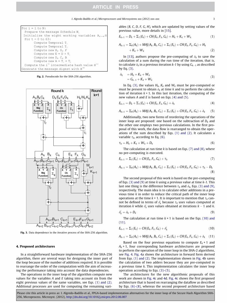
Fig. 2. Pseudocode for the SHA-256 algorithm.
Fig. 3. Data dependence in the iterative process of the SHA-256 algorithm.
I. Algredo-Badillo et al. / Microprocessors and Microsystems xxx (2012) xxx–xxx 3
4. Proposed architectures
In a straightforward hardware implementation of the SHA-256algorithm, there are several ways for designing the inner part ofthe loop because of the number of additions required. It is possibleto rearrange the order of the computation with the aim of increas-ing the performance taking into account the data dependencies.
The operations in the inner loop of the algorithm compute newvalues for the variables A and E taking into account six from theeight previous values of the same variables, see Eqs. (1) and (2).Additional processes are used for computing the remaining vari-
Please cite this article in press as: I. Algredo-Badillo et al., FPGA-based impleme256, Microprocess. Microsyst. (2012), http://dx.doi.org/10.1016/j.micpro.2012.
ables (B, C, D, F, G, H), which are updated by setting values of theprevious value, more details in [15].
Ekþ1 ¼ Dk þ R1ðEkÞ þ CHðEk; Fk;GkÞ þ Hk þ Kk þWk ð1Þ
Akþ1 ¼ R0ðAkÞ þMAJðAk;Bk;CkÞ þ R1ðEkÞ þ CHðEk; Fk;GkÞ þ Hk
þ Kk þWk ð2Þ
In [13], authors propose the pre-computing of dk to save thecalculation of a sum during the run time of the iteration, that is,to calculate dk in a previous iteration k-1 by using Gk�1 as describedby Eq. (3).
dk ¼ Hk þ Kk þWk
¼ Gk�1 þ Kk þWkð3Þ
In Eq. (3), the values Hk, Kk and Wk must be pre-computed ormust be present to obtain dk at time k and to perform the calcula-tion of iteration k + 1. In this last iteration, the computing of thenew values A and E is based on Eqs. (4) and (5).
Ekþ1 ¼ Dk þ R1ðEkÞ þ CHðEk; Fk;GkÞ þ dk ð4Þ
Akþ1 ¼ R0ðAkÞ þMAJðAk;Bk;CkÞ þ R1ðEkÞ þ CHðEk; Fk;GkÞ þ dk ð5Þ
Additionally, two new forms of reordering the operations of theinner loop are proposed: one based on the subtraction of Dk andthe other one employs two previous calculations. In the first pro-posal of this work, the data flow is rearranged to obtain the oper-ations of the sum described by Eqs. (1) and (2). It calculates avariable sk, according to Eq. (6).
sk ¼ Hk þ Kk þWk þ Dk ð6Þ
The calculation at run time k is based on Eqs. (7) and (8), whereno pre-computing is executed.
Ekþ1 ¼ R1ðEkÞ þ CHðEk; Fk;GkÞ þ sk ð7Þ
Akþ1 ¼ R0ðAkÞ þMAJðAk;Bk;CkÞ þ R1ðEkÞ þ CHðEk; Fk;GkÞ þ sk � Dk
ð8Þ
The second proposal of this work is based on the pre-computingof Eqs. (3) and (9) at time k using a previous value at time k-1. Thislast one thing is the difference between sk and dk, Eqs. (3) and (9),respectively. The main idea is to calculate other additions in a pre-vious time k in order to reduce the critical path of the inner loopoperations at the time k + 1. It is important to mention that sk can-not be defined in terms of d0k because sk uses values computed atiteration k while d0k uses values obtained at iterations k � 1 and k.
d0k ¼ dk þ Dk ð9Þ
The calculation at run time k + 1 is based on the Eqs. (10) and(11).
Ekþ1 ¼ R1ðEkÞ þ CHðEk; Fk;GkÞ þ d0k ð10Þ
Akþ1 ¼ R0ðAkÞ þMAJðAk;Bk;CkÞ þ R1ðEkÞ þ CHðEk; Fk;GkÞ þ dk ð11Þ
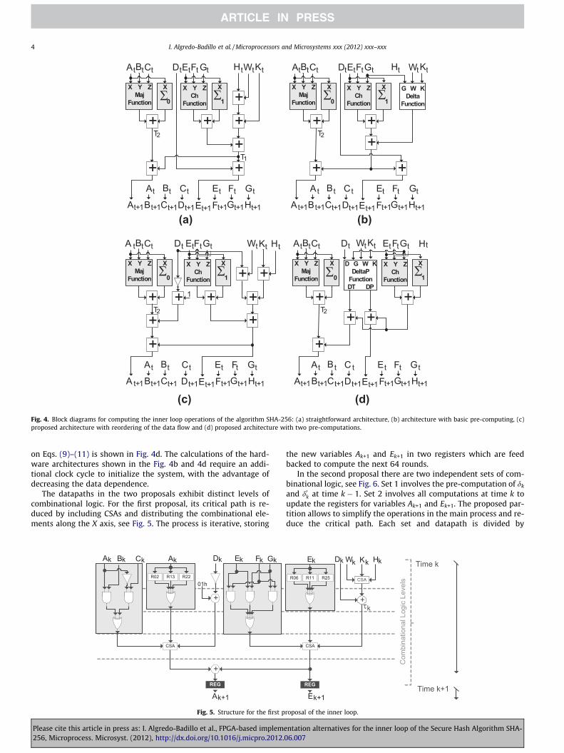
Based on the four previous equations to compute Ek + 1 andAk + 1, four corresponding hardware architectures are proposedto perform the operation of the inner loop in the SHA-2 algorithms,see Fig. 4. Fig. 4a shows the architecture in forward form derivedfrom Eqs. (1) and (2). The implementation shown in Fig. 4b savesthe calculation of two adders because they are pre-computed ina previous time k. This implementation calculates the inner loopoperation according to Eqs. (3)–(5).
The architectures for the new algorithmic proposals of thiswork are shown in Fig. 4c and 4d. Fig. 4c shows the first proposedarchitecture that is based on rearranging the dataflow as describedby Eqs. (6)–(8), whereas the second proposed architecture based
ntation alternatives for the inner loop of the Secure Hash Algorithm SHA-06.007
(a) (b)
(c) (d)Fig. 4. Block diagrams for computing the inner loop operations of the algorithm SHA-256: (a) straightforward architecture, (b) architecture with basic pre-computing, (c)proposed architecture with reordering of the data flow and (d) proposed architecture with two pre-computations.
4 I. Algredo-Badillo et al. / Microprocessors and Microsystems xxx (2012) xxx–xxx
on Eqs. (9)–(11) is shown in Fig. 4d. The calculations of the hard-ware architectures shown in the Fig. 4b and 4d require an addi-tional clock cycle to initialize the system, with the advantage ofdecreasing the data dependence.
The datapaths in the two proposals exhibit distinct levels ofcombinational logic. For the first proposal, its critical path is re-duced by including CSAs and distributing the combinational ele-ments along the X axis, see Fig. 5. The process is iterative, storing
Fig. 5. Structure for the first p
Please cite this article in press as: I. Algredo-Badillo et al., FPGA-based implem256, Microprocess. Microsyst. (2012), http://dx.doi.org/10.1016/j.micpro.2012.
the new variables Ak+1 and Ek+1 in two registers which are feedbacked to compute the next 64 rounds.
In the second proposal there are two independent sets of com-binational logic, see Fig. 6. Set 1 involves the pre-computation of dk
and d0k at time k � 1. Set 2 involves all computations at time k toupdate the registers for variables Ak+1 and Ek+1. The proposed par-tition allows to simplify the operations in the main process and re-duce the critical path. Each set and datapath is divided by
roposal of the inner loop.
entation alternatives for the inner loop of the Secure Hash Algorithm SHA-06.007
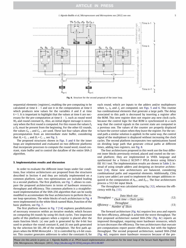
Fig. 6. Structure for the second proposal of the inner loop.
I. Algredo-Badillo et al. / Microprocessors and Microsystems xxx (2012) xxx–xxx 5
sequential elements (registers), enabling the pre-computing to becalculated at time k � 1 and use it in the computations at time kwhich produces new values for the variables A and E at timek + 1. It is important to highlight that the values at time k are nec-essary for the pre-computation at time k � 1, such as round wordWk and round constant Kk. Also, an initial digest message is neces-sary when the first round is computed. For this reason the values Fk
y Dk must be present from the beginning. For the other 63 rounds,the values Gk�1 and Ck�1 are used. These last four values allow theprecomputation from an intermediate state buffer, consideringthat Ht = Gt�1 and Dt = Ct�1, see Fig. 3.
The proposed structures shown in Figs. 5 and 6 for the innerloops are implemented and evaluated on two different platformsthat incorporate processes to compute the round word, round con-stant, state buffer and to control the dataflow of the entire SHA-2algorithm.
5. Implementation results and discussion
In order to evaluate the different inner loops under fair condi-tions, four relative architectures are proposed from the structuresdescribed in Section 4 and they are initially implemented on acommon platform. Later, two optimizations are included leadingto a second platform. The first platform, see Fig. 7, allows to com-pare the proposed architectures in terms of hardware resources,throughput and efficiency. This common platform is a straightfor-ward implementation of the SHA-256 algorithm that can be easilymodified to accommodate the four architectures to perform the in-ner loop operations. The white blocks of each architecture in Fig. 4were implemented in the white block named Main_Function of thebasic platform, see Fig. 7.
The first platform shown in Fig. 7 [14] explores parallelizationof necessary resources within an iterative module, which focuseson computing 64 rounds by using 64 clock cycles. Two importantpaths of this platform appears when a register is placed after themain function block: (a) one path is generated by the 6-bit busused to produce the round constant Kt and (b) one path generatedby the selection bit SEL_H0 of the multiplexer. The first path ap-pears when the ROM Memory64 � 32 is controlled by a 6-bit coun-ter. This counter generates addresses to select the constants Kt for
Please cite this article in press as: I. Algredo-Badillo et al., FPGA-based impleme256, Microprocess. Microsyst. (2012), http://dx.doi.org/10.1016/j.micpro.2012.
each round, which are inputs to the adders and/or multiplexerswhen sk, dk and d0k are computed, see Figs. 5 and 6. This routinehas combinational elements that generate a large path. The delayassociated to this path is decreased by inserting a register afterthe ROM. This new register does not require any new clock cycle,because the control logic for that ROM is synchronized in a suchway that the control signals in the current state are computed ina previous one. The values of the counter are properly displacedto have the correct values when they leave the register. For the sec-ond path a similar solution is applied. In the same way, the controlsignal of the multiplexer is displaced without increasing the clockcycles. The second platform incorporates two optimizations basedon dividing large path that generate critical paths at differenttimes, adding two registers, see Fig. 8.
The four architectures proposed in this work use the four differ-ent inner blocks previously revised, placed and routed on the sec-ond platform; they are implemented in VHDL language andsynthesized for a Virtex-2 XC2VP-7 FPGA device using Xilinx’sISE 10.1 tool. The implementation results are shown in Table 2. In-stead of using simple adders and designing an iterative architec-ture [14], these new architectures are balanced, consideringcombinational paths and sequential elements. Additionally, CSAs(carry save adder) are used to implement the integer additions re-quired in the computation of Ak+1 and Ek+1. The four architecturesprocess a 512-bit input block.
The throughput was calculated using Eq. (12), whereas the effi-ciency with Eq. (13).
Throughput ¼ Data block sizeClock time� Clock cycles
ð12Þ
Efficiency ¼ ThroughputNumber of Slices
ð13Þ
The forward architecture (Fig. 4a) requires less area and reportsthe best efficiency, although it achieved the worst throughput. Thefirst proposed architecture named SHA-256c (Fig. 4c) reports animproved throughput, requiring more hardware resources, whichin turn decreases the efficiency. The two architectures that executepre-computations report poorer efficiencies, but with the highestthroughput. The second proposed architecture, named SHA-256d(Fig. 4d), requires more hardware resources because of the pre-
ntation alternatives for the inner loop of the Secure Hash Algorithm SHA-06.007
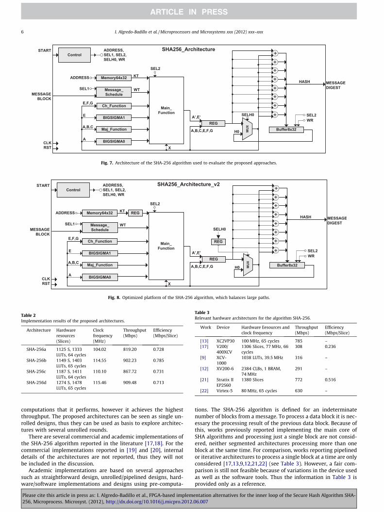
Fig. 7. Architecture of the SHA-256 algorithm used to evaluate the proposed approaches.
Fig. 8. Optimized platform of the SHA-256 algorithm, which balances large paths.
Table 2Implementation results of the proposed architectures.
Architecture Hardwareresources(Slices)
Clockfrequency(MHz)
Throughput(Mbps)
Efficiency(Mbps/Slice)
SHA-256a 1125 S, 1333LUTs, 64 cycles
104.02 819.20 0.728
SHA-256b 1149 S, 1403LUTs, 65 cycles
114.55 902.23 0.785
SHA-256c 1187 S, 1411LUTs, 64 cycles
110.10 867.72 0.731
SHA-256d 1274 S, 1478LUTs, 65 cycles
115.46 909.48 0.713
Table 3Relevant hardware architectures for the algorithm SHA-256.
Work Device Hardware Eesources andclock frequency
Throughput(Mbps)
Efficiency(Mbps/Slice)
[13] XC2VP30 100 MHz, 65 cycles 785 –[17] V200/
400XCV1306 Slices, 77 MHz, 66cycles
308 0.236
[9] XCV-1000
1038 LUTs, 39.5 MHz 316 –
[12] XV200-6 2384 CLBs, 1 BRAM,74 MHz
291 –
[21] Stratix IIEP2S60
1380 Slices 772 0.516
[22] Virtex-5 80 MHz, 65 cycles 630 –
6 I. Algredo-Badillo et al. / Microprocessors and Microsystems xxx (2012) xxx–xxx
computations that it performs, however it achieves the highestthroughput. The proposed architectures can be seen as single un-rolled designs, thus they can be used as basis to explore architec-tures with several unrolled rounds.
There are several commercial and academic implementations ofthe SHA-256 algorithm reported in the literature [17,18]. For thecommercial implementations reported in [19] and [20], internaldetails of the architectures are not reported, thus they will notbe included in the discussion.
Academic implementations are based on several approachessuch as straightforward design, unrolled/pipelined designs, hard-ware/software implementations and designs using pre-computa-
Please cite this article in press as: I. Algredo-Badillo et al., FPGA-based implem256, Microprocess. Microsyst. (2012), http://dx.doi.org/10.1016/j.micpro.2012.
tions. The SHA-256 algorithm is defined for an indeterminatenumber of blocks from a message. To process a data block it is nec-essary the processing result of the previous data block. Because ofthis, works previously reported implementing the main core ofSHA algorithms and processing just a single block are not consid-ered, neither segmented architectures processing more than oneblock at the same time. For comparison, works reporting pipelinedor iterative architectures to process a single block at a time are onlyconsidered [17,13,9,12,21,22] (see Table 3). However, a fair com-parison is still not feasible because of variations in the device usedas well as the software tools. Thus the information in Table 3 isprovided only as a reference.
entation alternatives for the inner loop of the Secure Hash Algorithm SHA-06.007
I. Algredo-Badillo et al. / Microprocessors and Microsystems xxx (2012) xxx–xxx 7
Considering implementation results from Table 3, the hardwarearchitectures proposed in this work report the highest throughputand efficiency, using fewer area resources.
In [12,23], forward architectures that calculate three hash func-tions, including the SHA-256, are reported; the implementation in[12] only computes the first stage of the algorithm. The works[17,9,21,22] report architectures with basic iterative architectures,where optimizations are done to decrease the critical path. In [9],authors propose to use three operands adders. It is important tohighlight that [13] proposes several optimizations for the innerloop using the function dk. The throughput reported in that workis 1.4 Gbps but this corresponds only to the architecture for com-puting the inner loop of SHA-2, not for the entire SHA-2 algorithm,for which the reached throughput is only 785 Mbps. The authorsuse circular buffer and save six adders to compute the final mes-sage digest. In this work, the results reported are for the completealgorithm with message schedule, 256-bit state buffer and controlunit, parallelizing different modules, large buses and eight final ad-ders. In [21], the reported architecture calculates three differenthash functions: MD5, SHA-1 and SHA 224/256, whereas [22] re-ports an architecture to perform the ciphering algorithm AES withdifferent key sizes and the hash functions SHA-1 and SHA-256.Some other works are implemented using different approachessuch as hardware/software co-design [24–26], or use of paralleliza-tion techniques, pipelining and loop unrolling [13,10,11,18].
6. Conclusion
Four new different schemes to improve the performance of thehardware implementation of the SHA-2 family were proposed.These architectures exhibit high performance, throughput and effi-ciency. The hardware designs are based on the rearrangement ofcomputation in the inner loop of SHA-2 algorithms, computingsome values in advance, balancing of paths, adding registers to re-duce paths by modifying control module without to increase clockcycles, and taking advantage of hardware architecture (paralleliza-tion, large buses and replicated components).
The proposed architectures use carry save adders, balancing ofdata paths and a state buffer to feedback the eight 32-bit registersthat keep the partial hashing needed to process each next datablock. The use of the state buffer helps to simplify the data pathsin the hardware architectures reducing the maximum delay inthe synthesized circuit. As a result, higher frequencies areachieved, minor area resources are used, and throughput is in-creased. The proposed architectures are improved by exploringthe algorithmic proposals for computing Ak+1 and Ek+1 and takingadvantage of hardware architectures. These modifications resultin hardware implementations with an improved efficiency andhigher throughput, while they slightly maintain a smaller use ofhardware resources.
Although the results were focused on the SHA-256 algorithm,these approaches can be extended to the other algorithms of theSHA-2 family due to their common structure, as well as to exploreother hardware techniques like the unrolling and pipelining.
References
[1] W. Stallings, Cryptography and Network Security, Prentice Hall, NJ, 2003.[2] R. Rivest, A. Shamir, L. Adleman, A method for obtaining digital signatures and
public-key cryptosystems, Communications of the ACM 21 (2) (1978) 120126.[3] American Bankers Association, ANSI X9.62-1998: public key cryptography for
the financial services industry: the elliptic curve digital signature algorithm(ECDSA), 1998.
[4] X. Wang, Y. Yin, H. Yu, Finding collisions in the full SHA-1, in: V. Shoup (Ed.),Advances in Cryptology CRYPTO 2005, Lecture Notes in Computer Science, vol.3621, Springer, Berlin, Heidelberg, 2005, pp. 17–36 (Chapter 2).
Please cite this article in press as: I. Algredo-Badillo et al., FPGA-based impleme256, Microprocess. Microsyst. (2012), http://dx.doi.org/10.1016/j.micpro.2012.
[5] P. Gauravaram, A. McCullagh, E. Dawson, Collision attacks on md5 and sha-1:is this the sword of damocles for electronic commerce? in: Proccedings ofAusCERT Asia Pacific Information Technology Security Conference(AUSCERT2006): Refereed R& D STREAM, 2006, pp. 73–88.
[6] E. Biham, R. Chen, A. Joux, P. Carribault, C. Lemuet, W. Jalby, Collisions of SHA-0and reduced SHA-1, in: R. Cramer (Ed.), Advances in Cryptology EUROCRYPT2005, Lecture Notes in Computer Science, vol. 3494, Springer, Berlin/Heidelberg, 2005, p. 577.
[7] A. Regenscheid, R. Perlner, S. Jen Chang, J. Kelsey, M. Nandi, S. Paul, Statusreport on the first round of the SHA-3 cryptographic hash algorithmcompetition, Tech. rep., NIST, September 2009.
[8] E. Andreeva, B. Mennink, B. Preneel, Security reductions of the second roundSHA-3 candidates, in: ISC, 2010, pp. 39–53.
[9] D. Fedoryka, Fast Implementation of the Secure Hash Algorithm SHA-256 inField Programmable Gate Arrays, George Mason University, 2004. <http://books.google.com/books?id=f009GwAACAAJ>.
[10] M. Zeghid, B. Bouallegue, M. Machhout, A. Baganne, R. Tourki, Architectural designfeatures of a programmable high throughput reconfigurable SHA-2 processor,Journal of Information Assurance and Security 2 (2008) (2007) 147–158.
[11] H.E. Michail, G.S. Athanasiou, A.A. Gregoriades, C.L. Panagiotou, C.E. Goutis,High throughput hardware/software co-design approach for SHA-256 hashingcryptographic module in IPSec/IPv6, Global Journal of Computer Science andTechnology 10 (4) (2010) 54–59.
[12] N. Sklavos, O. Koufopavlou, Implementation of the SHA-2 hash family standardusing FPGAs, The Journal of Supercomputing 31 (3) (2005) 227–248.
[13] R. Chaves, G. Kuzmanov, L. Sousa, S. Vassiliadis, Improving SHA-2 hardwareimplementations, in: CHES, 2006, pp. 298–310.
[14] I. Algredo-Badillo, C. Feregrino-Uribe, R. Cumplido, M. Morales-Sandoval,Novel hardware architecture for implementing the inner loop of the SHA-2algorithms, in: 14th Euromicro Conference on Digital System Design (DSD),IEEE Computer Society, Oulu, Finland, 2011, pp. 543–549.
[15] Federal Information Processing Standards Publication 180-2, Announcing theSecure Hash Standard. US DoC/NIST, August 2002.
[16] T. Wollinger, J. Guajardo, C. Paar, Security on FPGAs: state-of-the-artimplementations and attacks, ACM Transactions in Embedded ComputingSystems 3 (3) (2004) 534–574. http://dx.doi.org/10.1145/1015047.1015052.
[17] R. Glabb, L. Imbert, G. Jullien, A. Tisserand, N. Veyrat-Charvillon, Journal ofSystems Architecture 53 (2–3) (2007) 127–138. http://dx.doi.org/10.1016/j.sysarc.2006.09.006.
[18] R.P. McEvoy, F.M. Crowe, C.C. Murphy, W.P. Marnane, Optimisation of the SHA-2 family of hash functions on FPGAs, in: IEEE Computer Society AnnualSymposium on VLSI: Emerging VLSI Technologies and Architectures(ISVLSI’06), 2006, pp. 317–322.
[19] Helion Technology Limited, Fast SHA-256 hash core for Xilinx FPGA, datasheet.Revision 1.4, 2008.
[20] Helion Technology Limited, Tiny hash core family for Xilinx FPGA, datasheet.Revision 2.0, 2010.
[21] S. Ducloyer, R. Vaslin, G. Gogniat, E. Wanderley, Hardware implementation of amulti-mode hash architecture for MD5, SHA-1 and SHA-2, in: Workshop onDesign and Architectures for Signal and Image Processing, 2007.
[22] M. Togan, A. Floarea, G. Budariu, Design and implementation of cryptographicmodules on FPGA, in: Proceedings of the Applied Mathematics andInformatics, 2010, pp. 149–154.
[23] N. Sklavos, O. Koufopavlou, On the hardware implementations of the SHA-2(256, 384, 512) hash functions, in: Proceedings of IEEE InternationalSymposium on Circuits & Systems (IEEE ISCAS’03), 2003, pp. 153–156.
[24] M. As�kar, T. S�iltu Çelebi, Design and FPGA implementation of hash processor,in: Proceedings of the Information Security & Cryptology Conference withInternational Participation, 2007, pp. 85–89.
[25] K. Ting, S. Yuen, K. Lee, P. Leong, An FPGA based SHA-256 processor, in: M.Glesner, P. Zipf, M. Renovell (Eds.), Field-Programmable Logic andApplications: Reconfigurable Computing Is Going Mainstream, Lecture Notesin Computer Science, vol. 24, Springer, Berlin/Heidelberg, 2002, pp. 449–471.
[26] M. Juliato, C. Gebotys, Tailoring a reconfigurable platform to SHA-256 andHMAC through custom instructions and peripherals, in: InternationalConference on Reconfigurable Computing and FPGAs, IEEE Computer Society,Los Alamitos, CA, USA, 2009, pp. 195–200. http://doi.ieeecomputersociety.org/10.1109/ReConFig.2009.40.
Ignacio Algredo-Badillo received the B.Eng. from theInstituto Tecnologico de Puebla, Mexico, in 2002. Hereceived the M.Sc. degree from National Institute forAstrophysics, Optics, and Electronics (INAOE), Puebla,Mexico, in 2004. In 2008, he received the Ph.D. degree atINAOE. Currently, he is a professor-researcher at theUniversity of Istmo in Oaxaca, Mexico. He has involvedin the design and development of cryptographic sys-tems, reconfigurable architectures, software radio plat-forms, FPGA implementations, and application specifichardware acceleration.
ntation alternatives for the inner loop of the Secure Hash Algorithm SHA-06.007
8 I. Algredo-Badillo et al. / Microprocessors and Microsystems xxx (2012) xxx–xxx
Claudia Feregrino-Uribe is a researcher at the Com-puter Science Department at the National Institute forAstrophysics, Optics and Electronics (INAOE) in Puebla,Mexico. She received the M.Sc. degree from Centro deInvestigación y de Estudios Avanzados del InstitutoPolitécnico Nacional (CINVESTAV), Guadalajara and thePh.D. degree from Loughborough University in theUnited Kingdom. Her research areas are Data Com-pression, Cryptography and Steganography (Water-marking), Digital Systems Design, applications of FPGAs.She has served as a PC member for several conferences/workshops and as associate editor of the International
Journal of Reconfigurable Computing. She is member of the Researchers NationalSystem in Mexico and is founder member for the IEEE Puebla Computer SocietyChapter.
Rene Cumplido received the B.Eng. from the InstitutoTecnologico de Queretaro, Mexico, in 1995. He receivedthe M.Sc. degree from CINVESTAV Guadalajara, Mexico,in 1997 and the Ph.D. degree from Loughborough Uni-verity, UK in 2001. Since 2002 he is a professor at theComputer Science Department at INAOE in Puebla,Mexico. His research interests include the use of FPGAtechnologies, custom architectures and digital recon-figurable computing applications. He is co-founder andChair of the ReConFig international conference andfounder editor-in-chief of the International Journal ofReconfigurable Computing.
Please cite this article in press as: I. Algredo-Badillo et al., FPGA-based implem256, Microprocess. Microsyst. (2012), http://dx.doi.org/10.1016/j.micpro.2012.
Miguel Morales-Sandoval received the B.Sc. degree inComputer Science from the University of Puebla and theM.Sc. and Ph.D. degree in Computer Science from theNational Institute for Astrophysics, Optics and Elec-tronics (INAOE) in 2004 and 2008 respectively. Cur-rently he is a professor researcher at InformationTechnology department in the Polytechnic University ofVictoria, Mexico. His research areas include Public KeyCryptography, Elliptic Curve Cryptography, Data Com-pression, Reconfigurable Computing, and HDL HardwareDesign.
entation alternatives for the inner loop of the Secure Hash Algorithm SHA-06.007


![Evolving Hash Functions using Genetic Algorithmsajiips.com.au/papers/V4.1/V4N1.4 - Evolving Hash Functions using... · hash function called "PKP Hash" by Peter.K.Pearson [5] that](https://img.pdfslide.us/doc/110x75/5e3486a76e7276290f0add90/evolving-hash-functions-using-genetic-evolving-hash-functions-using-hash.jpg)