Embed Size (px)
Citation preview
Methodologies for the design of LCC voltage-outputresonant converters
M.P. Foster, H.I. Sewell, C.M. Bingham, D.A. Stone and D. Howe
Abstract: The paper presents five structured design methodologies for third-order LCC voltage-output resonant converters. The underlying principle of each technique is based on an adaptationof a FMA equivalent circuit that accommodates the nonlinear behaviour of the converter. Incontrast to previously published methods, the proposed methodologies explicitly incorporate theeffects of the transformer magnetising inductance. Furthermore, a number of the methodologiesallow the resonant-tank components to be specified at the design phase, thereby facilitating the useof standard off-the-shelf components. A procedure for sizing the filter capacitor is derived, and theuse of error mapping, to identify parameter boundaries and provide the designer with a qualitativefeel for the accuracy of a proposed converter design, is explored.
List of symbols
Cf filter capacitance (F)Cp parallel capacitance (F)Cs series capacitance (F)Ctot total equivalent-circuit capacitance (F)CZ equivalent load capacitance (F)Pf power factor
Iin peak input current (A)Iout output current (A)k rectifier coefficientLm transformer magnetising inductance (H)Ls series inductance (H)Mi resonant circuit to output-current ratioMv voltage-conversion ration transformer-turns ratioPout output power (W)Q equivalent-circuit quality factorQCf charge flowing through Cf (C)RL load resistance (O)RZ equivalent load resistance (O)Vb rectifier input voltage (V)vcp parallel capacitor voltage (V)Vdc DC input voltage (V)Vout output voltage (V)Ztot total equivalent-circuit impedance (O)a percentage-ripple-voltage specificationd1 rectifier nonconduction period (s)d2 Cf charging duration (s)y1 rectifier nonconduction angle (1)o0, f0 resonant frequency (rads�1,Hz)
on, fn normalised switching frequency (rads�1,Hz)os, fs switching frequency (rads�1,Hz)
1 Introduction
Increasingly, resonant power converters are becoming thepreferred technology for a wide variety of industrial,commercial- and consumer-product applications, owingmainly to their high power density. In part, this is facilitatedby a reduction in component size, due to the use of highswitching frequencies and the reduced heat-sinking require-ments, which results from their increased efficiency.Additionally, resonant converters offer the possibility ofexploiting transformer parasitics, such as the magnetisinginductance, leakage inductance and interwinding capaci-tance, directly in the resonant tank circuit, thereby reducingthe need for discrete components. Indeed, several compo-nent manufacturers have recognised the commercialpotential of resonant converters, and are producingdedicated resonant-converter-controller integrated circuits.
Although many resonant-converter topologies have beeninvestigated in the literature, it is the LCLC family ofconverters that has received the most attention. Particularmembers of the LCLC family offer significantly superioropen- and short-circuit behaviour compared with second-order counterparts, with some also exhibiting load-inde-pendent operating points [1, 2]. However, in contrast tosecond-order variants, the analysis and design of thesethird-order converters is complicated by the requirement tomodel more than one useful mode of operation.
Although the use of fundamental-mode-approximation(FMA) techniques for the analysis and design of resonantconverters [1–3] has been widespread, they suffer from anumber of limitations. First, as the switching frequencymoves away from the resonant frequency, the tank-currentwaveform becomes increasingly triangular, thereby invali-dating the sinusoidal-waveform assumption which isimplicit in the use of FMA. Secondly, the number of circuitstates that exist during a single switching cycle can changewith the operating condition. The LCC current-outputE-mail: [email protected]
M.P. Foster, C.M. Bingham, D.A. Stone and D. Howe are with the ElectricalMachines and Drives Group, Department of Electronic and ElectricalEngineering, University of Sheffield, Mappin Street, Sheffield S1 3JD, UK
H.I. Sewell is with Inductelec Ltd., Sheffield, UK
r The Institution of Engineering and Technology 2006
IEE Proceedings online no. 20050357
doi:10.1049/ip-epa:20050357
Paper first received 6th September and in final revised form 6th December 2005
IEE Proc.-Electr. Power Appl., Vol. 153, No. 4, July 2006 559
converter, for example, exhibits significant nonlinearbehaviour when heavily loaded [4], leaving the designerwith a degree of uncertainty as regards the appropriatenessof the chosen equivalent circuit. In an attempt to addresssuch issues, ‘modified’ FMA equivalent circuits, that moreaccurately represent the waveshape of a particular variable,have been developed. In [4], for instance, an equivalent-circuit model for the LCC current-output converteroperating under heavy- and intermediate-load conditionswas developed, by extracting the fundamental componentfrom an equation which described the nonsinusoidalparallel capacitor voltage. Other design/analysis methodol-ogies based on state–space models have also been reported,although they generally require the solution of nonlinearsimultaneous equations, which often requires recourse tonumerical methods and/or design charts [5, 6].
In this paper, five novel design-synthesis methodologiesfor LCC voltage-output converters are presented. All thetechniques enable the values of the resonant-circuitcomponents to be determined given a specified voltage-conversion factor, and a further specification particular tothe chosen methodology. The equivalent circuit is definedentirely in closed form, thereby making the proceduresdeterministic, and recourse to interpolation or complexnumerical solutions is not required. Further, a procedurefor sizing the filter capacitor is derived based on theequivalent-circuit model. The paper also introduces theconcept of confidence mapping to provide a mechanismfor assessing the accuracy of the results generated from aparticular design procedure, and give the designer a meansof fine tuning a converter’s performance. Thus, it has thepotential to reduce the design effort significantly, particu-larly during the initial phases, by identifying the viability ofa particular converter design and reducing the number ofsimulation verification steps which are normally required.
To reduce the complexity of the proposed designmethodologies, the following assumptions are made:
(i) All the passive components behave linearly;
(ii) Diodes are ideal one-way switches with an on-statevoltage drop;
(iii) MOSFETs are ideal switches with zero on-stateresistance;
(iv) All switches commutate instantaneously; and
(v) The converter input voltage is constant.
2 Equivalent-circuit modelling of LCCvoltage-output converter
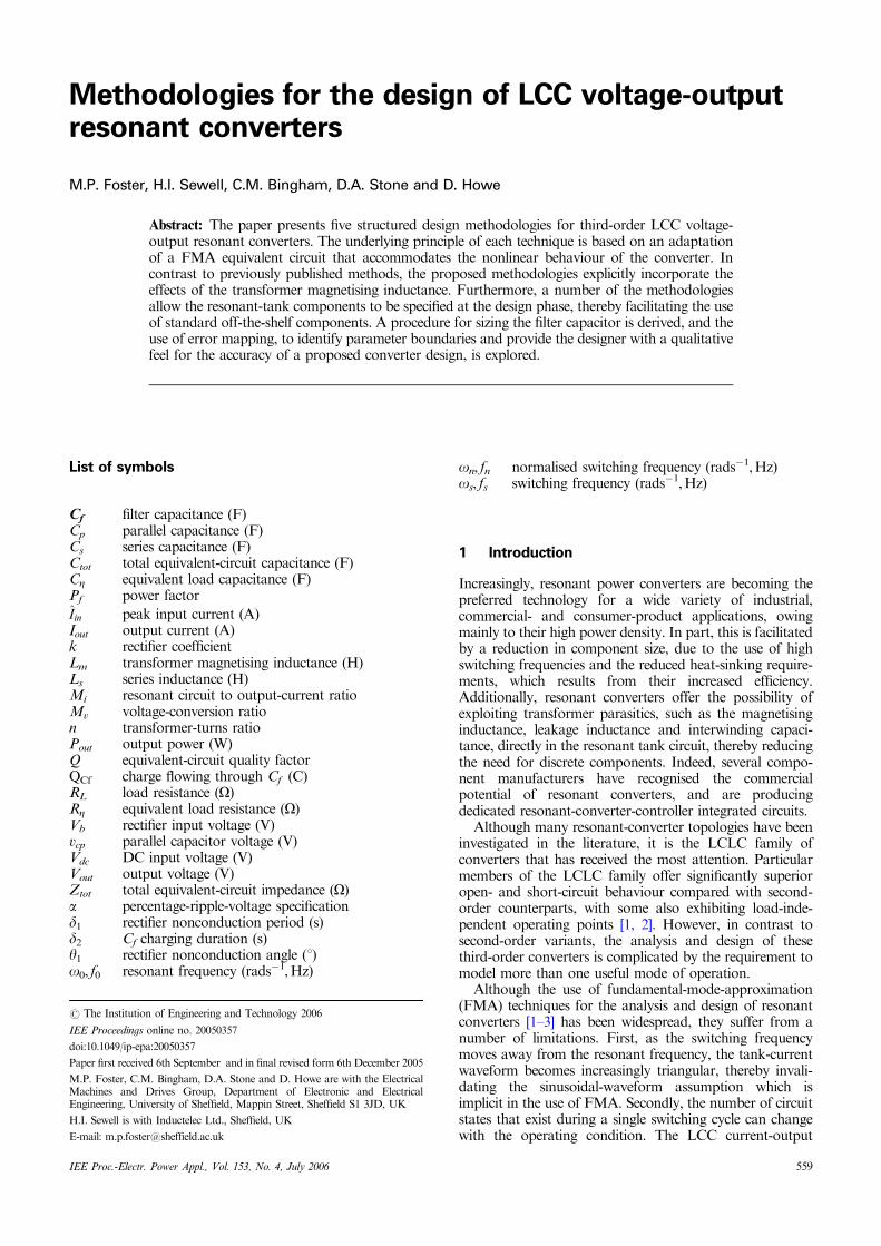
Consider the LCC voltage-output converter shown in Fig. 1in which the half-bridge MOSFETs T1 and T2 are switchedin antiphase at a frequency fs, thereby effectively ‘chopping’the DC link voltage Vdc to produce a square-wave inputvoltage Vi to the resonant tank. This excites the resonanttank and causes current iin to flow. The output voltage Vout
is developed from the portion of iin which flows into thefilter capacitor Cf when the rectifier is conducting, duringwhich time the parallel capacitor voltage vcp is clamped toVout. When iin crosses zero, the rectifier turns off and vcp falls(or rises) from Vout (�Vout) with a negative (positive) slope.When vcp ¼ �Vout, the rectifier commutates and clamps vcp
at �Vout. The rate at which vcp charges/discharges isdetermined by the values of Cp and RL.
The behaviour of the LCC converter is similar to that ofthe classical series-resonant converter [1, 3], with theexception that the rate-of-change of voltage at the input
to the bridge rectifier is limited by the presence of Cp.Moreover, it can be shown [6–9] that the interactionbetween Cp and Cf via the rectifier can produce a voltagegain greater than unity, a feature which is not possible witha classical second-order series converter.
Although the series-resonant converter is readily analysedusing FMA by replacing Vdc by an equivalent sinusoidalvoltage and representing the load and rectifier by anequivalent resistor Re, in practice this is not appropriate forthe LCC voltage-output-converter variant since vcp cannotbe assumed to have either a square or sinusoidal waveform,owing to the dv/dt-limiting effect of Cp. Consequently,a describing function is used to model vcp as a complexvoltage source, that is ultimately transformed into an‘equivalent’ complex impedance. This paper follows theapproaches taken in [7, 8], with the exception thatequivalent-circuit passive components are derived explicitlyand the effect of the rectifier on-state voltage is considered.The proposed analysis begins by assuming that the tank-current waveform is sinusoidal, i.e.
iin ¼ Iin sinðostÞ ð1Þwhere Iin is the peak value of iLs and os ¼ 2pfs is theangular switching frequency. This is justified since thefiltering action of the tank circuit removes high-orderharmonics, effectively forcing the input current to be asinusoid.
While the rectifier is conducting, the parallel capacitorvoltage is clamped to the output voltage, and is described by
vcp ¼ nðVout þ kVdÞsgnðiLsÞ ð2Þwhere k¼ 1 for a half-bridge rectifier or k¼ 2 for a full-bridge rectifier.
From Fig. 1b, the rectifier switches off when theresonant-circuit current, iin, crosses zero, at which time iinstarts to charge Cp. The period during which Cp is charging
a
Ls Cs
Cp
n :1
CfRL Vout
V
iRVdc
T1
T2 Vi
iin
7.6890 7.6895 7.6900 7.6905 7.6910 7.6915 7.6920 7.6925
−100
−50
0
50
100
150
time, ms
volta
ge/c
urre
nt ,
V/A
−150
b
Vivcpiin
�
Fig. 1 LCC voltage-output convertera Converterb Component waveforms
560 IEE Proc.-Electr. Power Appl., Vol. 153, No. 4, July 2006
can be obtained from the solution of
vcp ¼ vcp 0 þ1
Cp
Z d1
0
Iin sinðostÞdt ð3Þ
where d1 defines the end of the diode nonconduction periodand vcp 0} is the initial voltage on Cp. Solving for vcp
for the case when the initial condition is vcp 0 ¼ �nVb ¼�nðVout þ kVdÞ gives
vcp ¼ �nVb þIin
osCpf1� cosðostÞg ð4Þ
The charging time (or nonconduction period) can be foundby solving (4) for d1 to give
d1 ¼1
oscos�1 1� 2nosVbCp
Iin
� �¼ 1
osy1 ð5Þ
where y1 ¼ cos�1f1� ð2nosVbCp=IinÞg.The converter’s output current Iout is obtained by
determining the average current flowing through therectifier during a complete cycle. Defining the angle atwhich the rectifier starts to conduct as y1, the output currentis found from
Iout ¼n2p
Z p
y1Iin sinðyÞdyþ
Z 2p
y1þp�Iin sinðyÞdy
� �
¼ 2npðIin � VbosCP Þ ð6Þ
The output voltage is then readily determined from Ohm’slaw:
Vout ¼ 2nRLIin � knosCP Vd
pþ 2n2RLosCP
� �ð7Þ
To calculate Vout, Iin must be determined from theimpedance that the converter presents to the source. Tofacilitate this, vcp is converted into a complex voltage sourceusing describing-function techniques. Using (2)–(5), vcp isdescribed over a full cycle by
vcp ¼
�nVb þIin
osCpf1� cosðyÞg 0 � yoy1
nVb y1 � yop
nVb �Iin
osCpf1þ cosðyÞg y1 � yoy1 þ p
�nVb y1 þ p � yo2p
8>>>>>>>>><>>>>>>>>>:
ð8ÞThe describing function for vcp is obtained by extracting thefundamental from the Fourier series of (8). Substituting
for Vb and y1 and subsequently dividing by Iin gives theequivalent impedance Ze seen by the resonant circuit.Separating the equivalent impedance Ze into a resistivecomponent RZ and a capacitive component CZ gives
RZ ¼4ð2nRLIin þ kpVdÞðIin � 2nosCpVdÞ
g2I2in
CZ ¼pgCpIin2
gIinfnposCpð2nRLIin þ kpVdÞðIin � 2nosCpkVdÞg
p��
� fIinðg� 2pÞ þ 2nposCpkVdg
þ Iing p� cos�1ðg� 2pÞIin þ 2nposCpkVd
gIin
� �� ��ð9Þ
where g ¼ pþ 2osCpn2RL. Further information regardingthe derivation of RZ and CZ is given in [8].
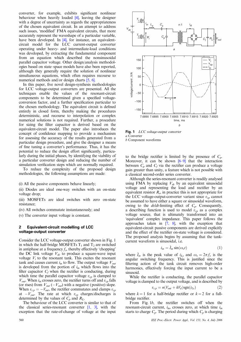
Inserting the series combination of RZ and CZ in place ofCp and its parallel components yields the equivalent seriescircuit for the converter shown in Fig. 2.
From standard circuit analysis, the total impedance Ztot
is given by
Ztot ¼ Ze þ j osLs �1
osCs
� �
¼ RZ þ j osLs �Cs þ CZ
osCsCZ
� �
¼ RZ þ j osLs �1
osCtot
� �ð10Þ
Hence, the magnitude of the input current, Iin, is obtainedfrom Ohm’s law as
Iin ¼Ve
jZtotjð11Þ
The output voltage is obtained by substituting (11) into (7).For analysis purposes, the calculation of CZ and RZ is
reliant on Iin, which is not generally known a priori.However, by setting Vd¼ 0 in (5), (9), (10) and (11), an
initial estimate for Iin (denoted with a prime) is obtainediteratively, as follows:
R0Z ¼8n2RL
g2
C0Z ¼pg2Cp
2n ð2posCpRLÞp
ðg�2pÞþg2 p�cos�1 g�2pg
� �� �ð12Þ
The total impedance seen at the source is thereforeestimated to be
Ztot ¼ R0Z þ j osLs �1
osC0tot
� �ð13Þ
An initial estimate of the input current immediately followsfrom (13), i.e.
I 0in ¼ð2=pÞVdc
R02Z þ osLs �1
osC0tot
� �2( )s ð14Þ
Once I 0in has been determined, an estimate ofVout can subsequently be refined using the following
Ls Cs
Rn
Cn
iin
Ve
Fig. 2 Equivalent circuit for LCC voltage-output converter
IEE Proc.-Electr. Power Appl., Vol. 153, No. 4, July 2006 561
procedure:
(a) Substitute I 0in and Vd into (5), (9), (10) and (11) to obtain
a revised value for Iin.
(b) Return to step 1 for the next iteration, or afterconvergence go to step 3.
(c) Finally, use the refined value of Iin to determine Vout
using (7).
Numerous simulation studies have shown that the foregoingiterative refinement procedure converges rapidly, with verylittle improvement in the results after the third iteration. Amore detailed description of the equivalent-circuit model isgiven in [9].
3 Design methodologies
This Section describes five novel design methodologiesbased on the equivalent-circuit model presented. Inaddition, a procedure for incorporating the magnetisinginductance of a transformer within the design of aconverter, along with a procedure for filter capacitor sizing,are also discussed.
The first methodology (designated DM1) bases thedesign on standard AC-circuit parameters (Q and o0) andthe rectifier nonconduction angle y1. The second methodol-ogy (DM2) employs the definition of the switch powerfactor, whilst the remaining methods (DM3–5) allow someresonant-circuit values to be specified during the designprocess, thereby allowing the designer to use standard ‘off-the-shelf’ components.
As with most design techniques, a standard set of core-specification parameters is required, summarised in Table 1.
3.1 Design method 1 (DM1): specifiedrectifier nonconduction angle y1In this method, all the resonant-circuit components (i.e.Ls, Cs and Cp) of the converter are determined for aspecific rectifier nonconduction angle y1, a given operatingfrequency fs and a combined equivalent resonant frequencyf0. Unlike the previously published techniques presented in[6, 7], the resonant-circuit-capacitor ratio (Cp/Cs) is notrequired, thereby making the interpretation of the designmore tangible. However, before presenting the designalgorithm in detail, it is instructive to consider howthe behaviour of the converter is influenced by theseparameters.
Analysis: In a similar manner to the normalising proceduredescribed in [3], the parameters Q, o0 and on can be usedto derive an expression for the voltage-conversion ratioMv ¼ Vo=Vdc, where
Q ¼ 1
o0CtotRZ¼ o0Ls
RZ; o0 ¼
1
ðLsCtotÞp ; on ¼
os
o0
ð15Þ
Specifically, from [3], Mv is obtained by combining (14) and(7)Fneglecting Vd, substituting into (15) and rearrangingusing (12), to give:
Mv ¼Vout
Vdc¼ 1
nf1þ cosðy1Þg1
1þ Q2 on �1
on
� �� �2s
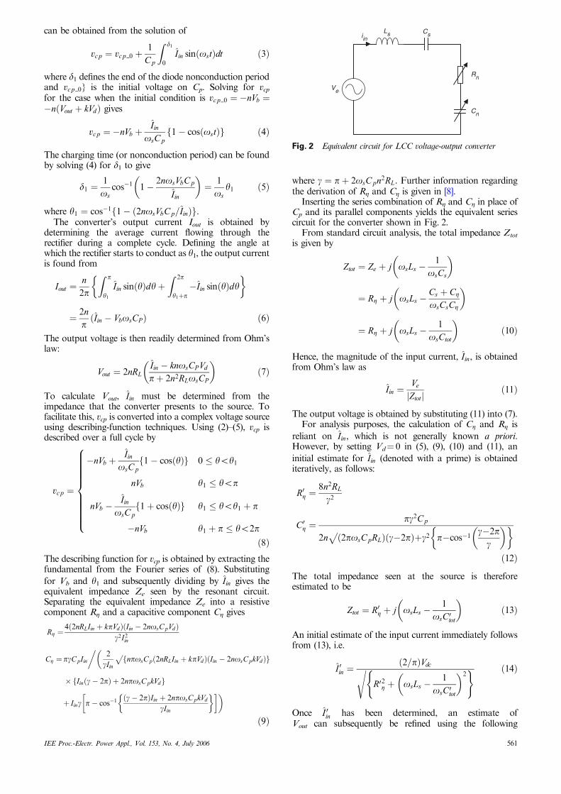
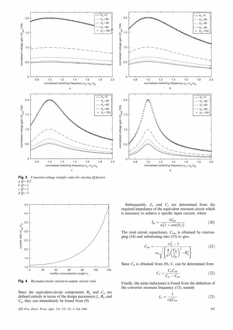
ð16ÞBy inspection, it can be seen that (16) has a similar form tothe standard series-resonant-converter FMA model [1, 3],with the exception that the gain is modified by the term1=½nf1þ cosðy1Þg�, which, importantly, shows the poten-tial for having a voltage gain greater than unity, as will beevident from Fig. 3. Moreover, from Fig. 3, it can be seenthat the voltage gain increases with the rectifier nonconduc-tion angle. This is expected since, when the rectifier is notconducting, Cp is being charged and can therefore support agreater voltage if charged for longer. Furthermore, Fig. 3shows that, while the magnitude of the voltage gain atresonance is unaffected by the Q-factor, the bandwidth, andhence the rate at which the voltage gain changes withfrequency, is significantly affected. This imposes restrictionson the maximum value of Q that can be employed in termsof the converter controllability and sensitivity to componenttolerances.
Although Fig. 3 provides useful information regardingthe voltage transfer and control characteristics of an LCCconverter, the designer is invariably also required tooptimise converter efficiency. However, rather than enteringinto a detailed discussion about the resonant tank,transformer and rectifier efficiencies (details of which canbe found elsewhere [1]), the ratio of the resonant-circuitcurrent to the output current Mi will be used as a metric fordesign. Setting Vd¼ 0 in (7), and substituting Vout ¼ IoutRL,using RMS quantities and rearranging, gives
Mi ¼Iin rms
Iout¼ p
2p
nf1þ cosðy1Þgð17Þ
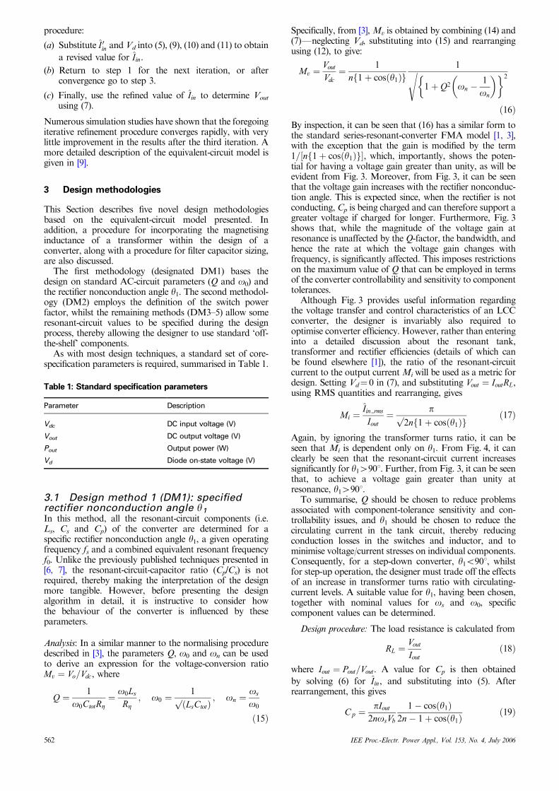
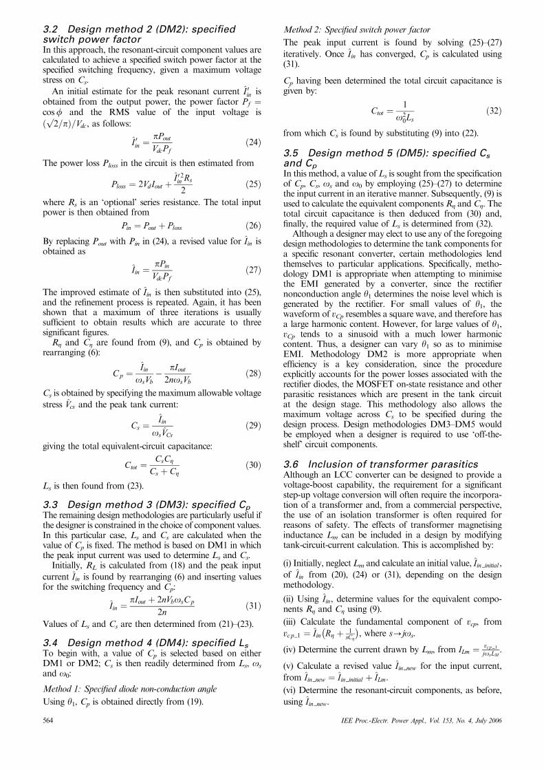
Again, by ignoring the transformer turns ratio, it can beseen that Mi is dependent only on y1. From Fig. 4, it canclearly be seen that the resonant-circuit current increasessignificantly for y14901. Further, from Fig. 3, it can be seenthat, to achieve a voltage gain greater than unity atresonance, y14901.
To summarise, Q should be chosen to reduce problemsassociated with component-tolerance sensitivity and con-trollability issues, and y1 should be chosen to reduce thecirculating current in the tank circuit, thereby reducingconduction losses in the switches and inductor, and tominimise voltage/current stresses on individual components.Consequently, for a step-down converter, y1o901, whilstfor step-up operation, the designer must trade off the effectsof an increase in transformer turns ratio with circulating-current levels. A suitable value for y1, having been chosen,together with nominal values for os and o0, specificcomponent values can be determined.
Design procedure: The load resistance is calculated from
RL ¼Vout
Ioutð18Þ
where Iout ¼ Pout=Vout. A value for Cp is then obtained
by solving (6) for Iin, and substituting into (5). Afterrearrangement, this gives
Cp ¼pIout
2nosVb
1� cosðy1Þ2n� 1þ cosðy1Þ
ð19Þ
Table 1: Standard specification parameters
Parameter Description
Vdc DC input voltage (V)
Vout DC output voltage (V)
Pout Output power (W)
Vd Diode on-state voltage (V)
562 IEE Proc.-Electr. Power Appl., Vol. 153, No. 4, July 2006
Since the equivalent-circuit components RZ and CZ aredefined entirely in terms of the design parameters fs, RL andCp, they can immediately be found from (9).
Subsequently, Ls and Cs are determined from therequired impedance of the equivalent resonant circuit whichis necessary to achieve a specific input current, where
Iin ¼pIout
nf1þ cosðy1Þgð20Þ
The total circuit capacitance, Ctot, is obtained by rearran-ging (14) and substituting into (15) to give
Ctot ¼o2
n � 1
os4
p2Vdc
Iin
� �2
�R2Z
( )s ð21Þ
Since CZ is obtained from (9), Cs can be determined from
Cs ¼CZCtot
CZ � Ctotð22Þ
Finally, the series inductance is found from the definition ofthe converter resonant frequency (15), namely
Ls ¼1
o20Ctot
ð23Þ
0.8 1.0 1.2 1.4 1.6 1.8 2.00
0.5
1.0
1.5
2.0
normalised switching frequency ωn=ωs / ω0
norm
alis
ed v
olta
ge g
ain
nVou
t / Vdc
a b
c d
0
0.5
1.0
1.5
2.0θ1=0
θ1=30
θ1=90θ1=120
θ1=60
0.8 1.0 1.2 1.4 1.6 1.8 2.0
0.8 1.0 1.2 1.4 1.6 1.8 2.00
0.5
1.0
1.5
2.0
0
0.5
1.0
1.5
2.0
norm
alis
ed v
olta
ge g
ain
nVou
t / Vdc
0.8 1.0 1.2 1.4 1.6 1.8 2.0
norm
alis
ed v
olta
ge g
ain
nVou
t / Vdc
normalised switching frequency ωn=ωs / ω0
norm
alis
ed v
olta
ge g
ain
nVou
t / Vdc
normalised switching frequency ωn=ωs / ω0 normalised switching frequency ωn=ωs / ω0
θ1=0
θ1=30
θ1=90θ1=120
θ1=60
θ1=0
θ1=30
θ1=90θ1=120
θ1=60
θ1=0
θ1=30
θ1=90θ1=120
θ1= 60
Fig. 3 Converter-voltage transfer ratio for varying Q-factorsa Q¼ 0.5b Q¼ 1c Q¼ 2d Q¼ 5
0 20 40 60 80 100 1201.0
1.5
2.0
2.5
3.0
3.5
4.0
4.5
rectifier nonconduction angle θ1
curr
ent
ratio
nI ou
t / Iin
Fig. 4 Resonant-circuit current-to-output current ratio
IEE Proc.-Electr. Power Appl., Vol. 153, No. 4, July 2006 563
3.2 Design method 2 (DM2): specifiedswitch power factorIn this approach, the resonant-circuit component values arecalculated to achieve a specified switch power factor at thespecified switching frequency, given a maximum voltagestress on Cs.
An initial estimate for the peak resonant current I 0in isobtained from the output power, the power factor Pf ¼cosf and the RMS value of the input voltage is
ð 2p
=pÞ=Vdc, as follows:
I 0in ¼pPout
VdcPfð24Þ
The power loss Ploss in the circuit is then estimated from
Ploss ¼ 2VdIout þI 0in
2Rs
2ð25Þ
where Rs is an ‘optional’ series resistance. The total inputpower is then obtained from
Pin ¼ Pout þ Ploss ð26ÞBy replacing Pout with Pin in (24), a revised value for Iin isobtained as
Iin ¼pPin
VdcPfð27Þ
The improved estimate of Iin is then substituted into (25),and the refinement process is repeated. Again, it has beenshown that a maximum of three iterations is usuallysufficient to obtain results which are accurate to threesignificant figures.
RZ and CZ are found from (9), and Cp is obtained byrearranging (6):
Cp ¼Iin
osVb� pIout
2nosVbð28Þ
Cs is obtained by specifying the maximum allowable voltage
stress Vcs and the peak tank current:
Cs ¼Iin
osVCsð29Þ
giving the total equivalent-circuit capacitance:
Ctot ¼CsCZ
Cs þ CZð30Þ
Ls is then found from (23).
3.3 Design method 3 (DM3): specified CpThe remaining design methodologies are particularly useful ifthe designer is constrained in the choice of component values.In this particular case, Ls and Cs are calculated when thevalue of Cp is fixed. The method is based on DM1 in whichthe peak input current was used to determine Ls and Cs.
Initially, RL is calculated from (18) and the peak input
current Iin is found by rearranging (6) and inserting valuesfor the switching frequency and Cp:
Iin ¼pIout þ 2nVbosCp
2nð31Þ
Values of Ls and Cs are then determined from (21)–(23).
3.4 Design method 4 (DM4): specified LsTo begin with, a value of Cp is selected based on eitherDM1 or DM2; Cs is then readily determined from Ls, os
and o0:
Method 1: Specified diode non-conduction angle
Using y1, Cp is obtained directly from (19).
Method 2: Specified switch power factor
The peak input current is found by solving (25)–(27)
iteratively. Once Iin has converged, Cp is calculated using(31).
Cp having been determined the total circuit capacitance isgiven by:
Ctot ¼1
o20Ls
ð32Þ
from which Cs is found by substituting (9) into (22).
3.5 Design method 5 (DM5): specified Csand CpIn this method, a value of Ls is sought from the specificationof Cp, Cs, os and o0 by employing (25)–(27) to determinethe input current in an iterative manner. Subsequently, (9) isused to calculate the equivalent components RZ and CZ. Thetotal circuit capacitance is then deduced from (30) and,finally, the required value of Ls is determined from (32).
Although a designer may elect to use any of the foregoingdesign methodologies to determine the tank components fora specific resonant converter, certain methodologies lendthemselves to particular applications. Specifically, metho-dology DM1 is appropriate when attempting to minimisethe EMI generated by a converter, since the rectifiernonconduction angle y1 determines the noise level which isgenerated by the rectifier. For small values of y1, thewaveform of vCp resembles a square wave, and therefore hasa large harmonic content. However, for large values of y1,vCp tends to a sinusoid with a much lower harmoniccontent. Thus, a designer can vary y1 so as to minimiseEMI. Methodology DM2 is more appropriate whenefficiency is a key consideration, since the procedureexplicitly accounts for the power losses associated with therectifier diodes, the MOSFET on-state resistance and otherparasitic resistances which are present in the tank circuitat the design stage. This methodology also allows themaximum voltage across Cs to be specified during thedesign process. Design methodologies DM3–DM5 wouldbe employed when a designer is required to use ‘off-the-shelf’ circuit components.
3.6 Inclusion of transformer parasiticsAlthough an LCC converter can be designed to provide avoltage-boost capability, the requirement for a significantstep-up voltage conversion will often require the incorpora-tion of a transformer and, from a commercial perspective,the use of an isolation transformer is often required forreasons of safety. The effects of transformer magnetisinginductance Lm can be included in a design by modifyingtank-circuit-current calculation. This is accomplished by:
(i) Initially, neglect Lm and calculate an initial value, Iin initial,
of Iin from (20), (24) or (31), depending on the designmethodology.
(ii) Using Iin, determine values for the equivalent compo-nents RZ and CZ using (9).
(iii) Calculate the fundamental component of vcp, from
vcp 1 ¼ Iin�RZ þ 1
sCZ
, where s-jos.
(iv) Determine the current drawn by Lm, from ILm ¼ vcp 1
josLM.
(v) Calculate a revised value Iin new for the input current,
from Iin new ¼ Iin initial þ ILm.
(vi) Determine the resonant-circuit components, as before,
using Iin new.
564 IEE Proc.-Electr. Power Appl., Vol. 153, No. 4, July 2006
3.7 Filter-capacitor sizingIn general, the value of Cf is chosen to satisfy the output-voltage-ripple specification, such that the ripple does notexceed a%. A suitable value for Cf is calculated byconsidering the charge which flows into Cf and thecorresponding voltage rise over a specific time interval.From the example waveforms shown in Fig. 5, it can beseen that, during the rectifier conduction period, the currentwhich flows into Cf is the difference between the rectifierinput and output currents.
Considering the period during which current is replenish-ing the charge on Cf, then
QCf ¼Z d2
d1iCf dt ¼
Z d2
d1fnIin sinðostÞ � Ioutgdt ð33Þ
where d2 is the time at which iCf becomes zero. d2 is foundfrom the solution of:
iCf ¼ nIin sinðostÞ � Iout ¼ 0
Therefore
d2 ¼1
osp� sin�1
Iout
nIin
� �� �ð34Þ
During this period Vout increases by an amount vrip, whichprovides a further expression for the charge flowing into Cf:
QCf ¼ Cf vrip ¼ Cf aVout ð35Þ
The minimum value of Cf which is required to limit vrip to aspecified level a is found by equating (33) and (35), andrearranging to give
Cf4nIin
aVoutosfcosðosd1Þ � cosðosd2Þg �
1
aRLðd2 � d1Þ
ð36Þ
If VoutcVd, (36) reduces to
Cf41
2aRLosðg2 � 4Þ
p� g
�þ 2 cos�1
g� 4RLosCP
g
� ��
þ sin�12
g
� ���ð37Þ
3.8 Experimental verificationTo demonstrate the validity of the proposed designmethodologies, a 25V-input, 35V-output, 22W experi-mental converter was designed to meet the specificationoutlined in Table 2 using DM4. The component values forthe remaining resonant-circuit components were deter-mined, using DM4, as Cp¼ 89nF, Cs¼ 224nF while thevalue for Cp was realised by paralleling four 22nFcapacitors to give 87nF measured and the value for Cs
created from a 220nF capacitor was connected in parallelwith two 2.2nF capacitors giving 224nF measured.
Operating as specified (i.e. with fs¼ 150kHz), theconverter had an output voltage of 33.6V which was within5% of the specification. Figure 6 shows the time-domainwaveforms of the input voltage to the tank (Vi) and theparallel capacitor voltage (vCp). Inspection of Fig. 6 showsthe diode nonconduction period y1 to be B1231, which isclose to the desired 1201.
4 Accuracy bounds
Classically, all FMA-based design methodologies assumethat voltage and current waveforms can readily beapproximated to sinusoids or square waves to simplifycircuit analysis. For the analysis described in this paper, theresonant circuit is assumed to respond only to thefundamental component of the input-voltage waveform(because of the filtering attributes of the tank) and asinusoidal current is therefore assumed to flow in theresonant circuit. However, for switching frequencies muchhigher than the resonant frequency (and for particular loadranges), the tank current becomes distorted, tending to atriangular waveshape, and thereby contravenes the FMAsinusoidal assumption. Consequently, there exists only asubset of converter parameters, obtained from FMAresults, that provide realisable converters having theexpected performance characteristics (see the account given[1], for instance).
19.536 19.5365 19.537 19.5375 19.538 19.5385 19.539 19.5395−40
−20
0
20
40
time, ms
−1.0
−0.5
0
0.5
1.0
volta
ge,
V
VR
ICf
iR
t = �1 t = �2
Iout
curr
ent,
A
Fig. 5 Voltage and current waveforms for filter capacitor
Table 2: Prototype converter parameters
Parameter Vdc
(V)Vout
(V)Pout
(W)Ls
(mH)fs(kHz)
f0s
(kHz)Q y1
(deg)n
Value 25 35 22 18.4 150 136 5.5 120 1
−8 −6 −4 0 2 4−50
−40
−30
−20
−10
0
10
20
30
40
50
time, µs
volta
ge,
V
Vv
−2
Vivcp
�1
Fig. 6 Voltage waveforms for prototype 22 W LCC voltage-outputconverter
IEE Proc.-Electr. Power Appl., Vol. 153, No. 4, July 2006 565
Here then, a comprehensive investigation is presented todetermine parameters that affect prediction performancesignificantly, by comparing results from over 250000simulation studies, obtained from an accurate nonlinearstate-variable model of the converter [10], with those fromthe equivalent-circuit model presented in Section 2, over abounded range of typical parameter valuesFspecifically,Vdc, Z0, the Q-factor, the ratio Cp/Cs ando0. The ranges aresummarised in Table 3. From the comparison of results,errors maps are generated to provide an indication of theexpected accuracy of a specific converter design. Justifica-tion for using the nonlinear-state-variable model as abenchmark metric is that no restrictions regarding thecircuit-voltage/current waveshapes or the interaction be-tween the output filter, rectifier and tank, are present, and itis therefore not constrained by underlying assumptions ofFMA.
By appropriate manipulation of the resulting data,so-called ‘2-D confidence maps’ that show the impact ofeach design parameter on the ‘confidence’ of a particularconverter design giving the expected performance, aregenerated. Since the parameters are applied to theequivalent-circuit model presented in Section 2, the resultingconfidence maps can be employed generically. In this case,the data are presented in a manner that can be appliediteratively in conjunction with design procedure DM1; seeFigs. 7–9. Although it is recognised that this type ofstatistical analysis only indicates relative trends, the bodyof evidence suggests that clearly defined regions ofparameter ranges exist where the designer can have a high‘confidence’ in realising expected performance from aparticular design procedure. For use with DM1, in thisexample, the diode voltage drop is assumed constant,(0.45V) in each case. Note that the normalised parametersthat have been selected in this case are among many thatcould have been chosen, including those relating to theratios Cp/Cs and RL/Zo, among others.
The procedure for generating the confidence maps issummarised below:
(i) Since, Qs ¼ fðp2=8RLÞ ðLs=CsÞp
g ¼ Z0=RL, RL is calcu-lated.
(ii) Since oos ¼ 1= ðLs=CsÞp
, Cs is calculated from,Cs ¼ 1=o0sZ0.
(iii) Using A¼Cp/Cs, Cp is calculated from Cp ¼ ACs.
(iv) Finally, Ls is determined from Ls ¼ Z20Cs.
The output-filter capacitor for each converter design isselected to limit the ripple on the output voltage to 1%.Finally, the nonlinear-converter model is simulated in thetime domain for 10�CfRL seconds to allow sufficient timeto achieve steady-state operation.
Table 3: Confidence-map-parameter ranges
Parameter Vdc (V) Qs Cp/Cs Z0 f0s (kHz) fs Vd (V)
Value 1–100 1–10 0.01–100 0.01–100 100 (1–2)� fr 0.45
0 2 4 6 8 100
20
40
60
80
100
120
140
160
180
Q-factor
θ 1
1
2
3
4
5
6
7
8
9
10
erro
r, %
Fig. 7 Output voltage prediction error as a function of y1 and Q-factor
0 2 4 6 8 100.8
1.0
1.2
1.4
1.6
1.8
2.0
Q-factor
1
2
3
4
5
6
7
8
9
10
8
ωn
erro
r, %
Fig. 8 Output voltage prediction error as a function of on andQ-factor
0.8 1.2 1. 1.6 1.8 2.00
0.2
0.4
0.6
0.8
1.2
1.4
1.6
1.8
1
2
3
4
5
6
7
8
9
10
erro
r, %
1.0 1.4
1.0
ωn
Mv
Fig. 9 Output voltage prediction error as a function of Mv and on
566 IEE Proc.-Electr. Power Appl., Vol. 153, No. 4, July 2006
The variable space on a confidence map is divided into agrid with each ‘pixel’ representing the level of predictionerror ( from 0 to 10%), the pixel value being determined bythe average ‘error’ within each element of the grid. Theprediction error is calculated from
Verror ¼Vout � Vout SS
Vout SS
� 100% ð38Þ
where Vout and Vout_ss are the output voltages obtainedfrom the equivalent-circuit model and the state-variablemodel, respectively.
Figure 7 shows the percentage error between thereference state-variable model and the equivalent-circuitmodel as a function of the rectifier nonconduction angle y1and the equivalent circuit Q-factor. It can be seen that thereexists a definite area, denoted by the dark regions, in whichthe equivalent-circuit-model predictions become inaccurate.With reference to Fig. 7, to ensure that accurate designpredictions can be made using the FMA-based designmethodologies, values of Q44 and y1o1201 should bechosen. However, limiting the rectifier nonconduction angley1o1201 also restricts the maximum voltage gain of theconverter to be less than 2 (see Fig. 3).
Figure 8 shows the prediction error as a function of theratio of the switching frequency and the ‘real’ resonantfrequency, denoted by on, and the equivalent circuitQ-factor. To have high confidence in realising a converterwith the required attributes, it is evident that it shouldbe designed to exhibit a relatively high Q-factor and,correspondingly, should be switched close to the resonantfrequency. This conforms to intuitive expectations, sincehigh Q-factor tank circuits provide low-distortion sinusoidaltank currents near resonance. However, as discussedpreviously, the designer must trade the effects of employinga high Q-factor against the effects on controllability andcomponent sensitivity. Figure 9 shows the design confidenceas a function of the voltage-conversion ratio Mv and theQ-factor, and reinforces these findings, since, for instance,confidence is highest for converter designs having Mv41and 1oono1.1, with the performance of most being within1% of that predicted from state-variable simulations, as aconsequence of the improved filtering of the excitation-voltage harmonics. Moreover, for converter designs requir-ing 0.5oMvo1, the results suggest that on should beo1.3,and, for gains less that 0.5, higher values of on should bechosen to ensure reasonable confidence in realising theexpected converter performance.
Although only a small sample of the possible error/confidence mappings have been presented (other keyvariants include confidence maps as functions of Mv againsty1 and y1 against on), it is apparent that they enableparameter boundaries to be viewed readily, therebyrestricting the design space. Moreover, although confidencemaps require significant computational effort to generate,ultimately, they are generic, and can be used as an integralpart of an interactive design tool. In practice, this isachieved by simultaneously placing a marker on each mapat intercepts which correspond to the converter designparameters. The underlying value on the confidence mapsthen indicates the prediction accuracy. A designer wouldthen interactively modify the converter design parametersso as to achieve a design that satisfied the specification to
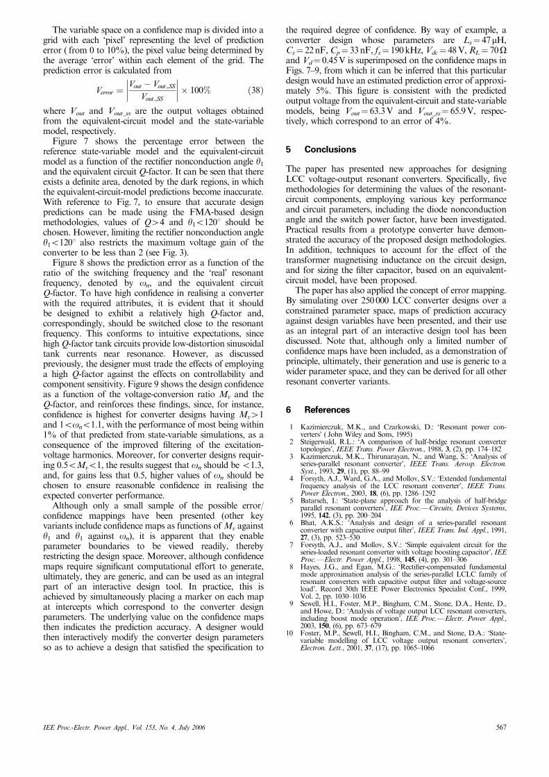
the required degree of confidence. By way of example, aconverter design whose parameters are Ls¼ 47mH,Cs¼ 22nF, Cp¼ 33nF, fs¼ 190kHz, Vdc¼ 48V, RL¼ 70Oand Vd¼ 0.45V is superimposed on the confidence maps inFigs. 7–9, from which it can be inferred that this particulardesign would have an estimated prediction error of approxi-mately 5%. This figure is consistent with the predictedoutput voltage from the equivalent-circuit and state-variablemodels, being Vout¼ 63.3V and Vout_ss¼ 65.9V, respec-tively, which correspond to an error of 4%.
5 Conclusions
The paper has presented new approaches for designingLCC voltage-output resonant converters. Specifically, fivemethodologies for determining the values of the resonant-circuit components, employing various key performanceand circuit parameters, including the diode nonconductionangle and the switch power factor, have been investigated.Practical results from a prototype converter have demon-strated the accuracy of the proposed design methodologies.In addition, techniques to account for the effect of thetransformer magnetising inductance on the circuit design,and for sizing the filter capacitor, based on an equivalent-circuit model, have been proposed.
The paper has also applied the concept of error mapping.By simulating over 250000 LCC converter designs over aconstrained parameter space, maps of prediction accuracyagainst design variables have been presented, and their useas an integral part of an interactive design tool has beendiscussed. Note that, although only a limited number ofconfidence maps have been included, as a demonstration ofprinciple, ultimately, their generation and use is generic to awider parameter space, and they can be derived for all otherresonant converter variants.
6 References
1 Kazimierczuk, M.K., and Czarkowski, D.: ‘Resonant power con-verters’ ( John Wiley and Sons, 1995)
2 Steigerwald, R.L.: ‘A comparison of half-bridge resonant convertertopologies’, IEEE Trans. Power Electron., 1988, 3, (2), pp. 174–182
3 Kazimierczuk, M.K., Thirunarayan, N., and Wang, S.: ‘Analysis ofseries-parallel resonant converter’, IEEE Trans. Aerosp. Electron.Syst., 1993, 29, (1), pp. 88–99
4 Forsyth, A.J., Ward, G.A., and Mollov, S.V.: ‘Extended fundamentalfrequency analysis of the LCC resonant converter’, IEEE Trans.Power Electron., 2003, 18, (6), pp. 1286–1292
5 Batarseh, I.: ‘State-plane approach for the analysis of half-bridgeparallel resonant converters’, IEE Proc.FCircuits, Devices Systems,1995, 142, (3), pp. 200–204
6 Bhat, A.K.S.: ‘Analysis and design of a series-parallel resonantconverter with capacitive output filter’, IEEE Trans. Ind. Appl., 1991,27, (3), pp. 523–530
7 Forsyth, A.J., and Mollov, S.V.: ‘Simple equivalent circuit for theseries-loaded resonant converter with voltage boosting capacitor’, IEEProc.FElectr. Power Appl., 1998, 145, (4), pp. 301–306
8 Hayes, J.G., and Egan, M.G.: ‘Rectifier-compensated fundamentalmode approximation analysis of the series-parallel LCLC family ofresonant converters with capacitive output filter and voltage-sourceload’. Record 30th IEEE Power Electronics Specialist Conf., 1999,Vol. 2, pp. 1030–1036
9 Sewell, H.I., Foster, M.P., Bingham, C.M., Stone, D.A., Hente, D.,and Howe, D.: ‘Analysis of voltage output LCC resonant converters,including boost mode operation’, IEE Proc.FElectr. Power Appl.,2003, 150, (6), pp. 673–679
10 Foster, M.P., Sewell, H.I., Bingham, C.M., and Stone, D.A.: ‘State-variable modelling of LCC voltage output resonant converters’,Electron. Lett., 2001, 37, (17), pp. 1065–1066
IEE Proc.-Electr. Power Appl., Vol. 153, No. 4, July 2006 567