Embed Size (px)
Citation preview
www.elsevier.com/locate/elecom
Electrochemistry Communications 6 (2004) 1042–1044
Metallization of multi-walled carbon nanotubes with copperby an electroless deposition process
Feng Wang a, Susumu Arai a,*, Morinobu Endo b
a Department of Chemistry and Material Engineering, Faculty of Engineering, Shinshu University,
4-17-1 Wakasato, Nagano-shi, Nagano 380-8553, Japanb Department of Electrical and Electronic Engineering, Faculty of Engineering, Shinshu University, 4-17-1 Wakasato,
Nagano-shi, Nagano 380-8553, Japan
Received 2 August 2004; received in revised form 9 August 2004; accepted 9 August 2004
Abstract
An advantageous procedure has been developed, allowing metallization of multi-walled carbon nanotubes (MWCNTs, mean
diameter: 50–80 nm) with Cu layer by an electroless deposition process. Such a procedure for achieving electroless Cu deposition
on MWCNTs involves acid pre-clean, sensitization and activation. Results show that metallizated MWCNTs keep the fiber-like
appearances with uniform distribution. This resulting nanotube-derived material is comprised of a nanocrocrystalline Cu layer
and inner nanotube covered with Cu layer. The results of this work have demonstrated the effectiveness of electroless deposition
on the metallization of MWCNTs.
� 2004 Elsevier B.V. All rights reserved.
Keywords: Metallization; Carbon nanotube; Electroless deposition; Copper layer
1. Introduction
Multi-walled carbon nanotube (MWCNT) is an ideal
raw material for various applications due to its out-
standing mechanical characteristics such as high tensile
strength and high elastic modulus, high thermal conduc-
tivity and electric conductivity [1,2]. Recently, there has
been great interest in the metallization of MWCNTs
[3,4] for creating new metal-matrix-based carbon tubecomposites. This metallization process firstly belongs
to a kind of surface modification of MWCNTs, not only
can increase the surface active sites to improve bonding
between nanotube and resin or ceramic [5], but also can
maintain the superior performance and excellent intrin-
sic properties of MWCNTs in the composites. Further-
1388-2481/$ - see front matter � 2004 Elsevier B.V. All rights reserved.
doi:10.1016/j.elecom.2004.08.007
* Corresponding author. Tel.: +81 26 269 5413; fax: +81 26 269
5432.
E-mail address: [email protected] (S. Arai).
more, this metallization of MWCNTs has been shown tohave significant potential for the fabrication of new
powder MWCNT-metal composites [6,7], thus extend-
ing the application fields of MWCNTs.
Such metallization of MWCNTs can be achieved via
an electroless deposition process at normal temperature
state. To obtain the MWCNTs covered with a continual
Cu layer, a pre-treatment procedure comprised of acid
pre-clean, sensitization and activation is essential to pur-ify MWCNTs and increase the catalytic sites on
MWCNTs. In this study, nitric acid was used to pre-
clean the MWCNTs, and so-called �two-step� processwas performed to impart the catalyzation effect to the
surface of MWCNTs for the subsequent electroless Cu
deposition [8]. Moreover, MWCNTs tend to aggregate
into packed ropes or entangled networks due to strong
inter-tube van der Waals attraction, which may hinderthe formation of Cu-deposited MWCNTs with homog-
enous distribution. Here, one cationic polymer was used
F. Wang et al. / Electrochemistry Communications 6 (2004) 1042–1044 1043
to disperse MWCNTs in the aqueous solution on each
pre-treatment step and subsequent electroless deposition
process.
The aim of this work was to develop an advantageous
procedure allowing the metallization of the MWCNTs
with copper layers. An effective deposition bath contain-ing glyoxalic acid as reductant was designed, and then
was used to electrolessly deposited Cu layer on
MWCNTs. The microstructures of resulting Cu-
MWCNT composites were characterized with the help
of field emission scanning electron microscope (FE-
SEM), X-ray diffraction (XRD) and transmission elec-
tron microscope (TEM).
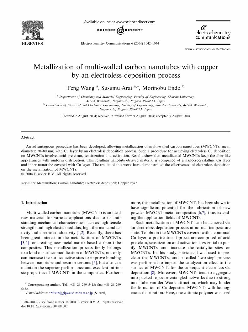
Fig. 1. SEM image of Cu-deposited MWCNTs.
2. Experimental
The MWCNTs used were synthesized via catalyst as-
sisted CVD (Showa Denko Co. Ltd) [9]. They were then
heat-treated at 2800 �C under an argon flow for 30 min
to form graphitic layer structure. MWCNTs were typi-
cally 50–80 nm in diameter and 10–20 lm in averagelength.
The electroless deposition bath was composed of 0.03
M CuSO4 Æ 5H2O as the metal ions source, 0.25 M ED-
TA Æ 2Na as the complexing agent and 0.1 M CHO-
COOH Æ H2O as the reductant. All solutions were
prepared using deionized water and reagent grade
chemicals.
MWCNTs were pre-cleaned in 12.8 M concentratedHNO3 for 12 h and rinsed thoroughly with deionized
water. The pre-clean preformed by nitric acid is to pur-
ify the MWCNTs, especially to eliminate the residual
metal catalyst particles from the carbon tube prepara-
tion process by CVD [10] for avoiding their side-effect
in the subsequent electroless deposition process. Moreo-
ver, the acid pre-clean also can slightly modify the sur-
face of MWCNTs, and then can enhance theinterfacial adhesion between MWCNT and metal film
[11].
The pre-cleaned MWCNTs were then sensitized in
the aqueous solution containing 0.0089 M SnCl2 and
0.0024 M HCl for 10 min, and activated in an aqueous
solution containing 0.0012 M PdCl2 and 0.012 M HCl
for 30 min, followed by rinsing thoroughly with deion-
ized water. In the ‘‘two-steps’’ method, the sensitizationis to improve the adsorption of Sn2+ on the MWCNT
surfaces. The activation then can be done to form the
fine Pd particles on MWCNT surfaces through the dis-
placement reaction between Sn2+ and Pd2+. At this step,
Pd particles serve as seeds for catalytic nucleating
centers.
Finally the pre-treated MWCNTs were immersed in
the electroless Cu plating bath with magnetic stirreragitation. On each step, MWCNTs were dispersed by
adding 1.25 · 10�6 M poly(diallyldimethylammonium
chloride) solution (mean molecular weight 400000;
PDMA, Aldrich) in the aqueous solution. The plating
cell was a beaker of 200 cm3, and the electroless deposi-
tion temperature was 60 �C. The deposition time was
controlled as 10 min. The deposited MWCNTs were
then filtered and rinsed with deionized water, then driedat room temperature in a vacuum desiccator.
The morphological features of Cu-deposited
MWCNTs were observed with the help of FE-SEM
(S-4100, HITACHI). The phase structures were deter-
mined by XRD (RINT2200V/PC, RIGAKU) and
high-resolution TEM (JEM-2000FE, JEOL).
3. Results and discussion
FE-SEM has been used to observe the morphological
features of Cu-deposited MWCNTs. The Cu-deposited
MWCNTs in the diameter of 130–180 nm are present
clearly in Fig. 1, showing the fiber-like appearance of
composites with a homogenous distribution. This indi-
cates that the above pre-treatment procedure used toachieve the metallization of MWCNTs with Cu layer
by an electroless deposition process is effective. The
resulting nanotube-derived composite is comprised of
polycrystalline Cu layer and inner MWCNT covered
with Cu layer.
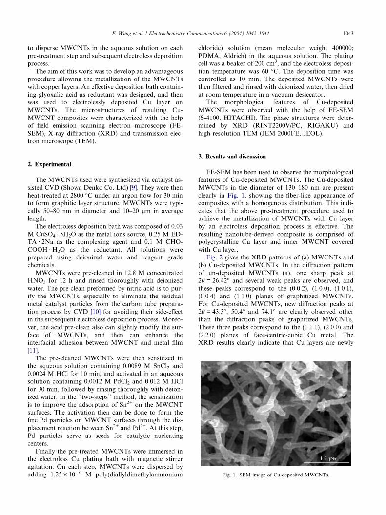
Fig. 2 gives the XRD patterns of (a) MWCNTs and
(b) Cu-deposited MWCNTs. In the diffraction pattern
of un-deposited MWCNTs (a), one sharp peak at2h = 26.42� and several weak peaks are observed, and
these peaks correspond to the (0 0 2), (1 0 0), (1 0 1),
(0 0 4) and (1 1 0) planes of graphitized MWCNTs.
For Cu-deposited MWCNTs, new diffraction peaks at
2h = 43.3�, 50.4� and 74.1� are clearly observed other
than the diffraction peaks of graphitized MWCNTs.
These three peaks correspond to the (1 1 1), (2 0 0) and
(2 2 0) planes of face-centric-cubic Cu metal. TheXRD results clearly indicate that Cu layers are newly
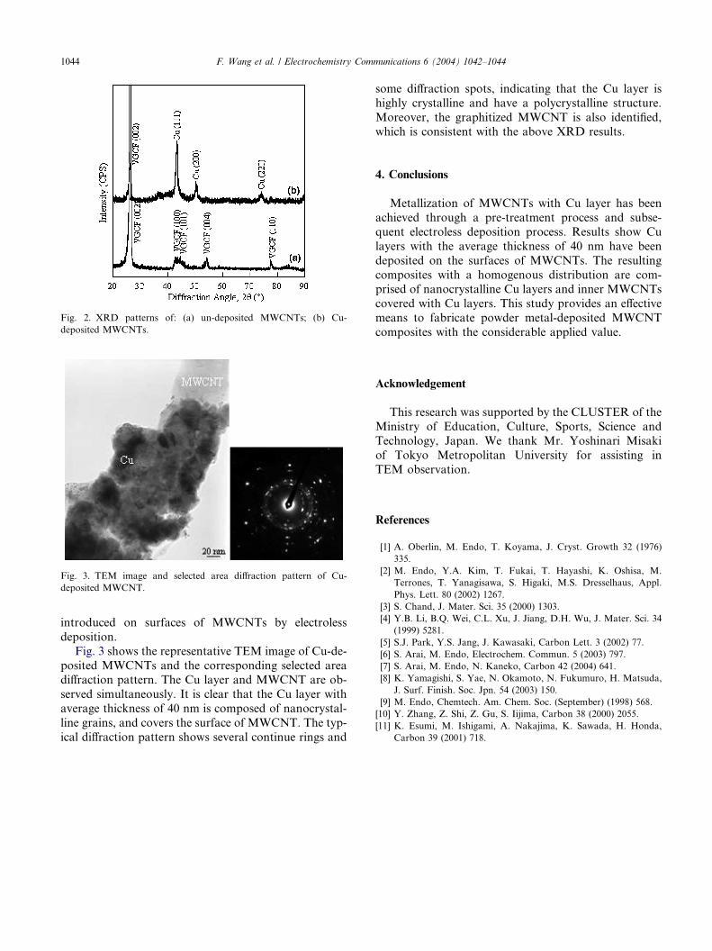
Fig. 3. TEM image and selected area diffraction pattern of Cu-
deposited MWCNT.
Fig. 2. XRD patterns of: (a) un-deposited MWCNTs; (b) Cu-
deposited MWCNTs.
1044 F. Wang et al. / Electrochemistry Communications 6 (2004) 1042–1044
introduced on surfaces of MWCNTs by electroless
deposition.
Fig. 3 shows the representative TEM image of Cu-de-
posited MWCNTs and the corresponding selected areadiffraction pattern. The Cu layer and MWCNT are ob-
served simultaneously. It is clear that the Cu layer with
average thickness of 40 nm is composed of nanocrystal-
line grains, and covers the surface of MWCNT. The typ-
ical diffraction pattern shows several continue rings and
some diffraction spots, indicating that the Cu layer is
highly crystalline and have a polycrystalline structure.
Moreover, the graphitized MWCNT is also identified,
which is consistent with the above XRD results.
4. Conclusions
Metallization of MWCNTs with Cu layer has been
achieved through a pre-treatment process and subse-
quent electroless deposition process. Results show Cu
layers with the average thickness of 40 nm have been
deposited on the surfaces of MWCNTs. The resulting
composites with a homogenous distribution are com-prised of nanocrystalline Cu layers and inner MWCNTs
covered with Cu layers. This study provides an effective
means to fabricate powder metal-deposited MWCNT
composites with the considerable applied value.
Acknowledgement
This research was supported by the CLUSTER of the
Ministry of Education, Culture, Sports, Science and
Technology, Japan. We thank Mr. Yoshinari Misaki
of Tokyo Metropolitan University for assisting in
TEM observation.
References
[1] A. Oberlin, M. Endo, T. Koyama, J. Cryst. Growth 32 (1976)
335.
[2] M. Endo, Y.A. Kim, T. Fukai, T. Hayashi, K. Oshisa, M.
Terrones, T. Yanagisawa, S. Higaki, M.S. Dresselhaus, Appl.
Phys. Lett. 80 (2002) 1267.
[3] S. Chand, J. Mater. Sci. 35 (2000) 1303.
[4] Y.B. Li, B.Q. Wei, C.L. Xu, J. Jiang, D.H. Wu, J. Mater. Sci. 34
(1999) 5281.
[5] S.J. Park, Y.S. Jang, J. Kawasaki, Carbon Lett. 3 (2002) 77.
[6] S. Arai, M. Endo, Electrochem. Commun. 5 (2003) 797.
[7] S. Arai, M. Endo, N. Kaneko, Carbon 42 (2004) 641.
[8] K. Yamagishi, S. Yae, N. Okamoto, N. Fukumuro, H. Matsuda,
J. Surf. Finish. Soc. Jpn. 54 (2003) 150.
[9] M. Endo, Chemtech. Am. Chem. Soc. (September) (1998) 568.
[10] Y. Zhang, Z. Shi, Z. Gu, S. Iijima, Carbon 38 (2000) 2055.
[11] K. Esumi, M. Ishigami, A. Nakajima, K. Sawada, H. Honda,
Carbon 39 (2001) 718.


![Electroless metallization of polymers69 Electroless metallization of polymers Volume 74 Issue 2 August 2015 plastic and metal [10-12]. Thus, the properties of surface layer material](https://img.pdfslide.us/doc/110x75/5ed2293f718a6e7cc9070257/electroless-metallization-of-69-electroless-metallization-of-polymers-volume-74.jpg)