Embed Size (px)
Citation preview
1
MEMS Overview, Prof. A. Mason Page 1
MEMS OverviewSPEAKER• Andrew Mason, Asst. Professor in Electrical and Computer Engineering
TOPIC• Overview of Micro-Electro-Mechanical Systems (MEMS)
OUTLINE• Overview of MEMS & Microsystems Navid Yazdi
• Micromachining & MEMS process technology Navid Yazdi
• Micro-electro-mechanical devices & microsensors– Inertial sensors Navid Yazdi
– Pressure sensors Navid Yazdi
– Bio-sensors Andrew Mason
– Shock sensors Andrew Mason
• Integrated Microsystems Andrew Mason
MEMS Overview, Prof. A. Mason Page 2
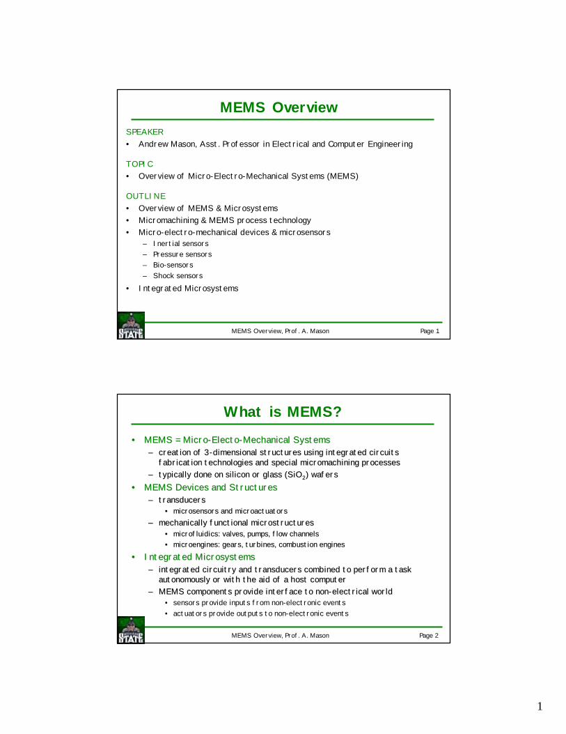
What is MEMS?
•• MEMS = MicroMEMS = Micro--ElectoElecto--Mechanical SystemsMechanical Systems–– creation of 3creation of 3--dimensional structures using integrated circuits dimensional structures using integrated circuits
fabrication technologies and special fabrication technologies and special micromachining micromachining processesprocesses–– typically done on silicon or glass (SiOtypically done on silicon or glass (SiO22) wafers) wafers
•• MEMS Devices and StructuresMEMS Devices and Structures–– transducerstransducers
•• microsensors and microsensors and microactuatorsmicroactuators–– mechanically functional microstructuresmechanically functional microstructures
•• microfluidicsmicrofluidics: valves, pumps, flow channels: valves, pumps, flow channels•• microenginesmicroengines: gears, turbines, combustion engines: gears, turbines, combustion engines
•• Integrated MicrosystemsIntegrated Microsystems–– integrated circuitry and transducers combined to perform a task integrated circuitry and transducers combined to perform a task
autonomously or with the aid of a host computerautonomously or with the aid of a host computer–– MEMS components provide interface to nonMEMS components provide interface to non--electrical worldelectrical world
• sensors provide inputs from non-electronic events• actuators provide outputs to non-electronic events
2
MEMS Overview, Prof. A. Mason Page 3
Why Use MEMS?•• Motivation and BenefitsMotivation and Benefits
–– Small SizeSmall Size–– Light Weight Light Weight –– Enhanced Performance & ReliabilityEnhanced Performance & Reliability
•• high resolution devices high resolution devices •• array of devicesarray of devices
–– Low Cost (from batch fabrication)Low Cost (from batch fabrication)
•• ApplicationsApplications–– Automotive SystemAutomotive System–– Health Care Health Care –– Automated Manufacturing Automated Manufacturing –– InstrumentationInstrumentation–– Environmental Monitoring & ControlEnvironmental Monitoring & Control–– Consumer ProductsConsumer Products–– AerospaceAerospace
•• MEMSMEMS--basedbasedMicrosystemsMicrosystems
–– highly integrated systemshighly integrated systems–– sensing sensing –– actuationactuation–– computationcomputation–– controlcontrol–– communicationcommunication
MEMS Overview, Prof. A. Mason Page 4
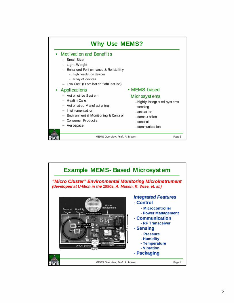
Example MEMS-Based Microsystem
Microcontroller
RF Transmitter
PressureSensor
HumiditySensor
I/O ConnectorOn/Off Switch
Accelerometer
PowerManagement
InterfaceChips
60mm
35m
m
Integrated FeaturesIntegrated Features-- ControlControl
-- MicrocontrollerMicrocontroller-- Power ManagementPower Management
-- Communication Communication -- RF TransceiverRF Transceiver
-- SensingSensing-- PressurePressure-- Humidity Humidity -- TemperatureTemperature-- Vibration Vibration
-- PackagingPackaging
“Micro Cluster” Environmental Monitoring Microinstrument“Micro Cluster” Environmental Monitoring Microinstrument(developed at U(developed at U--Mich Mich in the 1990s, A. Mason, K. Wise, et. al.)in the 1990s, A. Mason, K. Wise, et. al.)
3
MEMS Overview, Prof. A. Mason Page 5
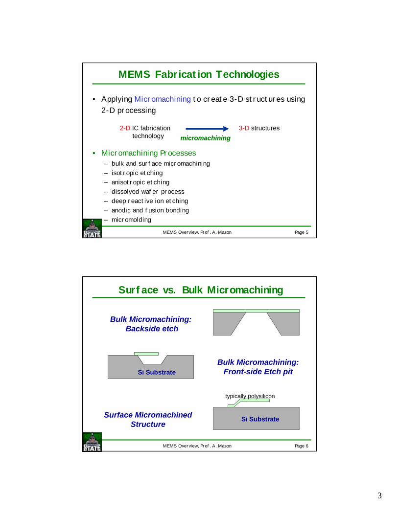
MEMS Fabrication Technologies
• Applying Micromachining to create 3-D structures using 2-D processing
• Micromachining Processes– bulk and surface micromachining– isotropic etching– anisotropic etching– dissolved wafer process– deep reactive ion etching– anodic and fusion bonding– micromolding
micromachiningmicromachining2-D IC fabrication 3-D structures
technology
MEMS Overview, Prof. A. Mason Page 6
Surface vs. Bulk Micromachining
Bulk Micromachining: Backside etch
Si SubstrateSurface Micromachined Structure
Si SubstrateBulk Micromachining:
Front-side Etch pit
typically polysilicon
4
MEMS Overview, Prof. A. Mason Page 7
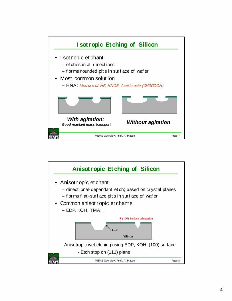
Isotropic Etching of Silicon
• Isotropic etchant– etches in all directions– forms rounded pits in surface of wafer
• Most common solution– HNA: Mixture of HF, HNO3, Acetic acid (CH3COOH)
With agitation: Good reactant mass transport Without agitation
MEMS Overview, Prof. A. Mason Page 8
Anisotropic Etching of Silicon
Anisotropic wet etching using EDP, KOH: (100) surface- Etch stop on (111) plane
(100) Surface orientation
Silicon
54.74°
(111) Surface orientation
• Anisotropic etchant– directional-dependant etch; based on crystal planes– forms flat-surface pits in surface of wafer
• Common anisotropic etchants– EDP, KOH, TMAH
5
MEMS Overview, Prof. A. Mason Page 9
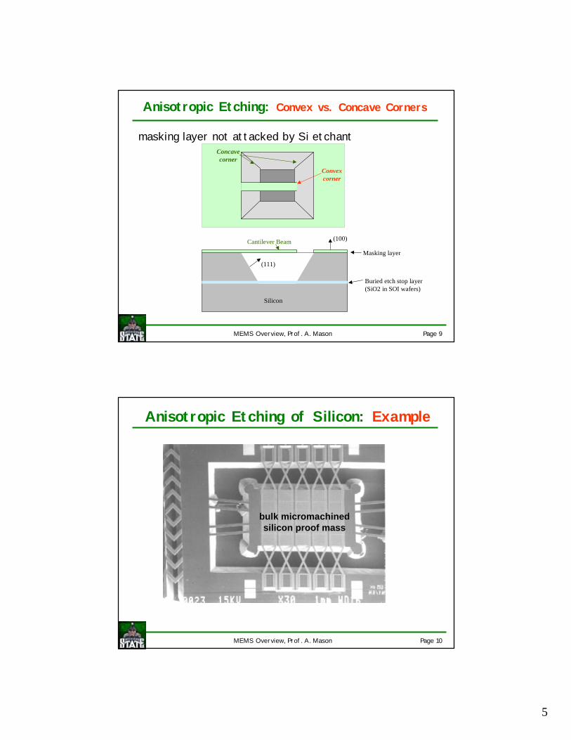
Anisotropic Etching: Convex vs. Concave Corners
Top View
Convex corner
Concave corner
(111)
Silicon
Buried etch stop layer (SiO2 in SOI wafers)
Masking layer
Cantilever Beam
Side View
(100)
masking layer not attacked by Si etchant
MEMS Overview, Prof. A. Mason Page 10
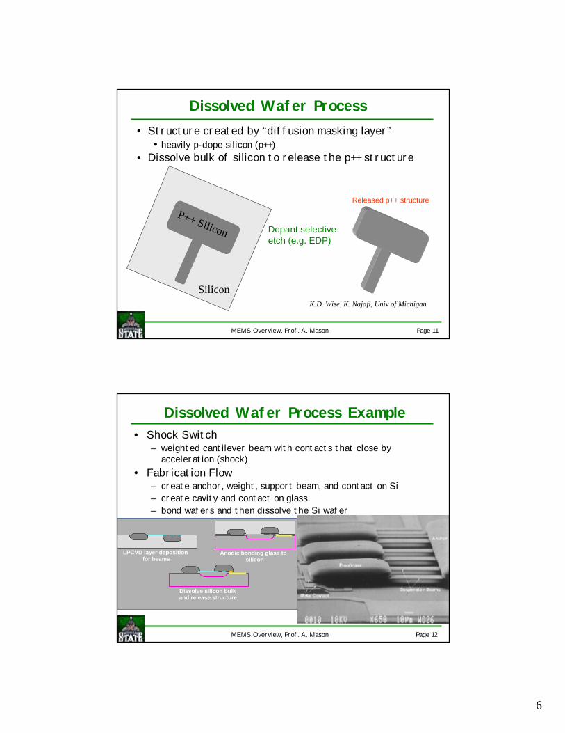
Anisotropic Etching of Silicon: Example
bulk micromachined bulk micromachined silicon proof masssilicon proof mass
6
MEMS Overview, Prof. A. Mason Page 11
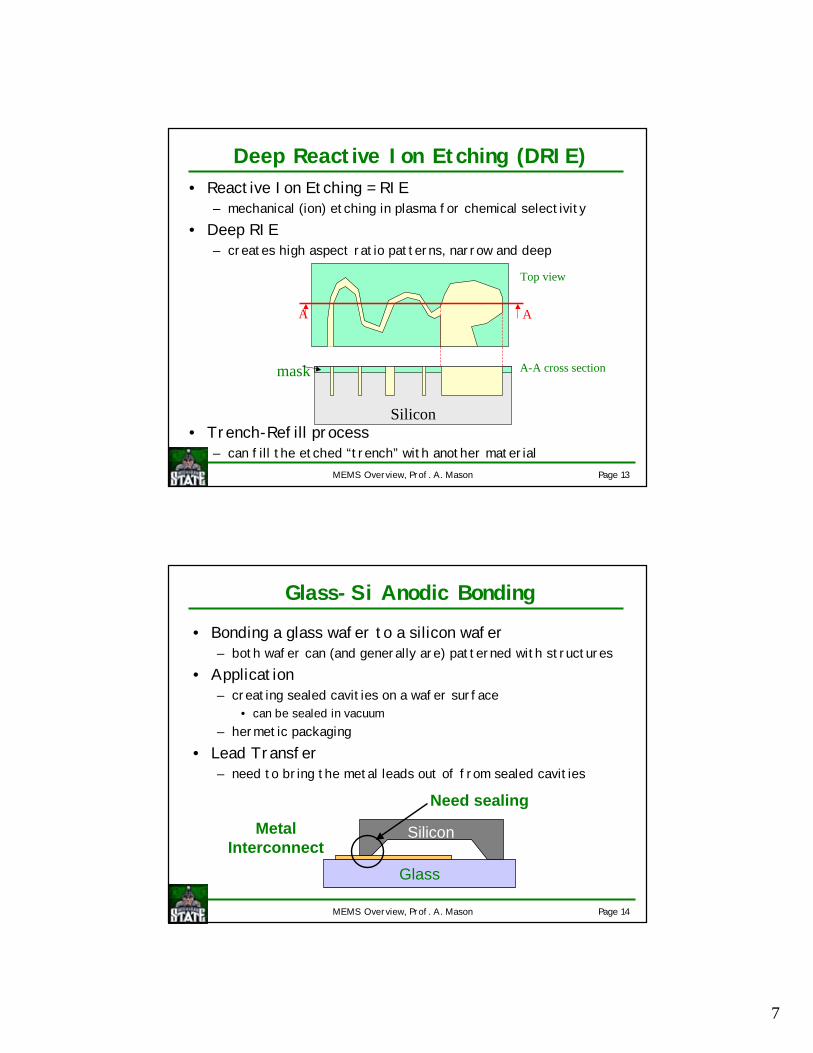
Dissolved Wafer Process
Silicon
P++ Silicon Dopant selective etch (e.g. EDP)
• Structure created by “diffusion masking layer”• heavily p-dope silicon (p++)
• Dissolve bulk of silicon to release the p++ structure
K.D. Wise, K. Najafi, Univ of Michigan
Released p++ structure
MEMS Overview, Prof. A. Mason Page 12
Dissolved Wafer Process Example• Shock Switch
– weighted cantilever beam with contacts that close by acceleration (shock)
• Fabrication Flow– create anchor, weight, support beam, and contact on Si– create cavity and contact on glass– bond wafers and then dissolve the Si wafer
LPCVD layer depositionfor beams
Anodic bonding glass tosilicon
Dissolve silicon bulkand release structure
7
MEMS Overview, Prof. A. Mason Page 13
Deep Reactive Ion Etching (DRIE)• Reactive Ion Etching = RIE
– mechanical (ion) etching in plasma for chemical selectivity• Deep RIE
– creates high aspect ratio patterns, narrow and deep
• Trench-Refill process– can fill the etched “trench” with another material
Top view
A-A cross section
AA
mask
Silicon
MEMS Overview, Prof. A. Mason Page 14
Glass-Si Anodic Bonding
• Bonding a glass wafer to a silicon wafer– both wafer can (and generally are) patterned with structures
• Application– creating sealed cavities on a wafer surface
• can be sealed in vacuum– hermetic packaging
• Lead Transfer– need to bring the metal leads out of from sealed cavities
Glass
SiliconMetal Interconnect
Need sealing
8
MEMS Overview, Prof. A. Mason Page 15
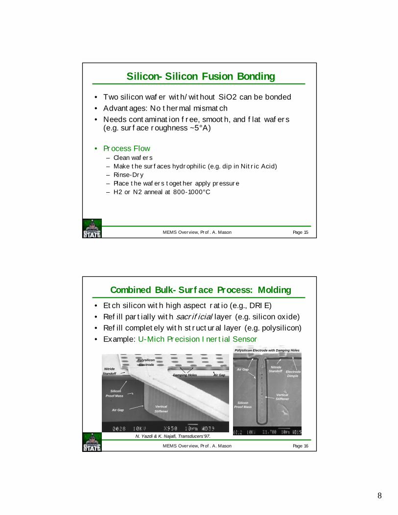
Silicon-Silicon Fusion Bonding
• Two silicon wafer with/without SiO2 can be bonded• Advantages: No thermal mismatch• Needs contamination free, smooth, and flat wafers
(e.g. surface roughness ~5°A)
• Process Flow– Clean wafers– Make the surfaces hydrophilic (e.g. dip in Nitric Acid)– Rinse-Dry– Place the wafers together apply pressure– H2 or N2 anneal at 800-1000°C
MEMS Overview, Prof. A. Mason Page 16
Combined Bulk-Surface Process: Molding• Etch silicon with high aspect ratio (e.g., DRIE)• Refill partially with sacrificial layer (e.g. silicon oxide)• Refill completely with structural layer (e.g. polysilicon)• Example: U-Mich Precision Inertial Sensor
SiliconProof Mass
VerticalStiffenerAir Gap
PolysiliconElectrode
Damping Holes
NitrideStandoff Air Gap
VerticalStiffener
Polysilicon Electrode with Damping Holes
Air GapElectrodeDimple
NitrideStandoff
SiliconProof Mass
N. Yazdi & K. Najafi, Transducers’97.N. Yazdi & K. Najafi, Transducers’97.
9
MEMS Overview, Prof. A. Mason Page 17
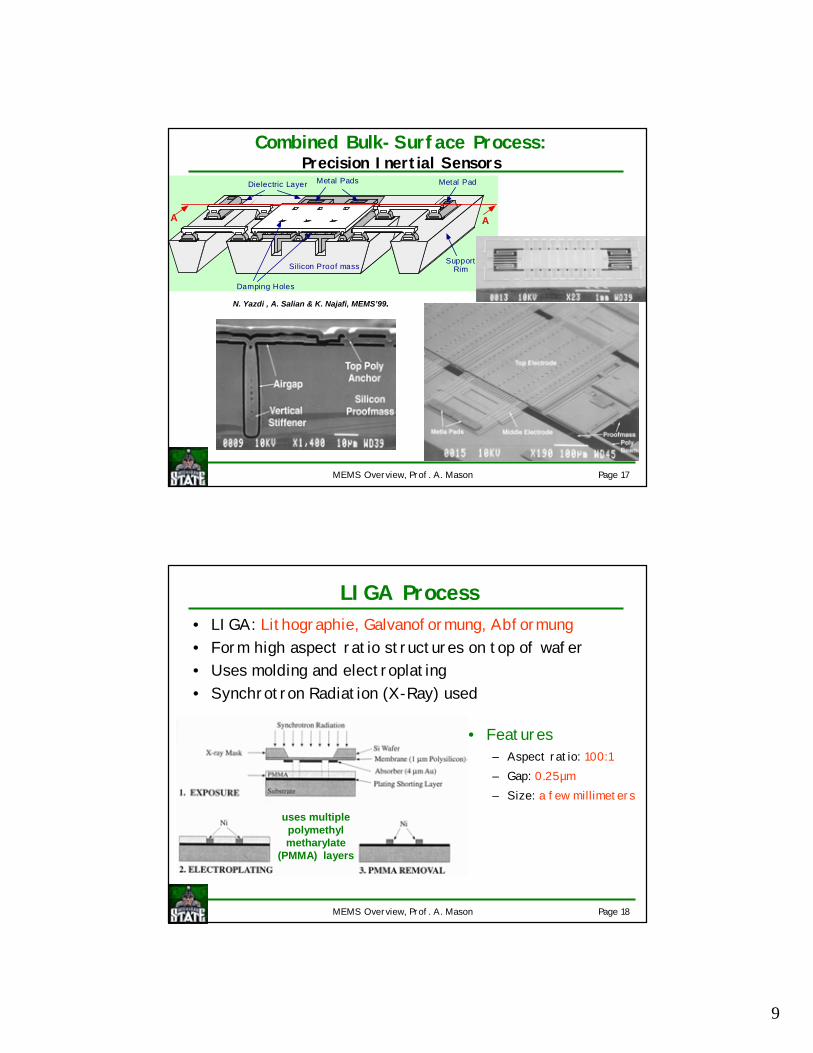
Combined Bulk-Surface Process:Precision Inertial Sensors
N. Yazdi , A. Salian & K. Najafi, MEMS’99..
Dielectric Layer
SupportRimSilicon Proof mass
A A
Damping Holes
Metal Pads Metal Pad
MEMS Overview, Prof. A. Mason Page 18
LIGA Process• LIGA: Lithographie, Galvanoformung, Abformung• Form high aspect ratio structures on top of wafer• Uses molding and electroplating• Synchrotron Radiation (X-Ray) used
uses multiple polymethyl metharylate
(PMMA) layers
• Features– Aspect ratio: 100:1– Gap: 0.25µm– Size: a few millimeters
10
MEMS Overview, Prof. A. Mason Page 19
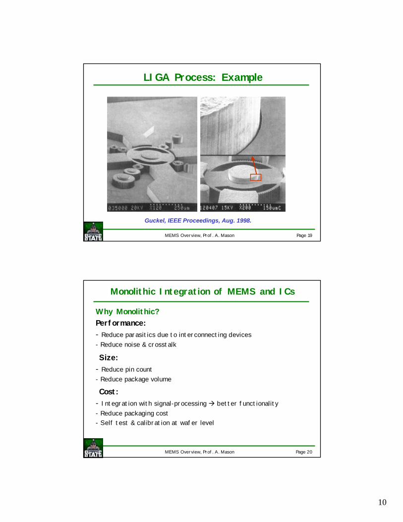
LIGA Process: Example
Guckel, IEEE Proceedings, Aug. 1998.
MEMS Overview, Prof. A. Mason Page 20
Why Monolithic?Performance:- Reduce parasitics due to interconnecting devices- Reduce noise & crosstalk
Size:- Reduce pin count- Reduce package volume
Cost:- Integration with signal-processing � better functionality- Reduce packaging cost- Self test & calibration at wafer level
Monolithic Integration of MEMS and ICs
11
MEMS Overview, Prof. A. Mason Page 21
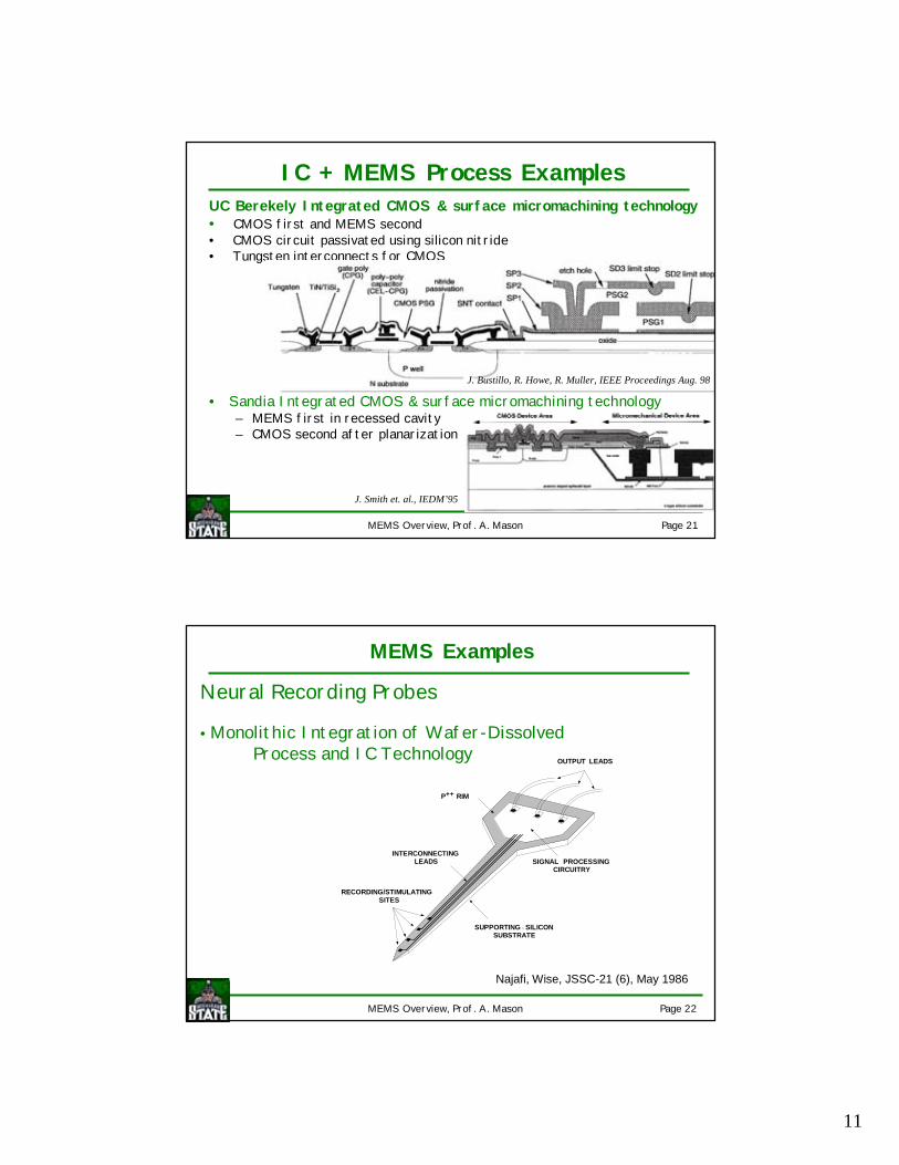
IC + MEMS Process ExamplesUC Berekely Integrated CMOS & surface micromachining technology• CMOS first and MEMS second • CMOS circuit passivated using silicon nitride• Tungsten interconnects for CMOS
• Sandia Integrated CMOS & surface micromachining technology– MEMS first in recessed cavity– CMOS second after planarization
J. Bustillo, R. Howe, R. Muller, IEEE Proceedings Aug. 98
J. Smith et. al., IEDM’95
MEMS Overview, Prof. A. Mason Page 22
- Neural probes with signal processing circuitry- P++ shanks- P++ rim and timed etch to protect active circuitry
MEMS Examples
OUTPUT LEADS
SIGNAL PROCESSINGCIRCUITRY
RECORDING/STIMULATING SITES
INTERCONNECTINGLEADS
SUPPORTING SILICONSUBSTRATE
P++ RIM
Najafi, Wise, JSSC-21 (6), May 1986
Neural Recording Probes
• Monolithic Integration of Wafer-DissolvedProcess and IC Technology
12
MEMS Overview, Prof. A. Mason Page 23
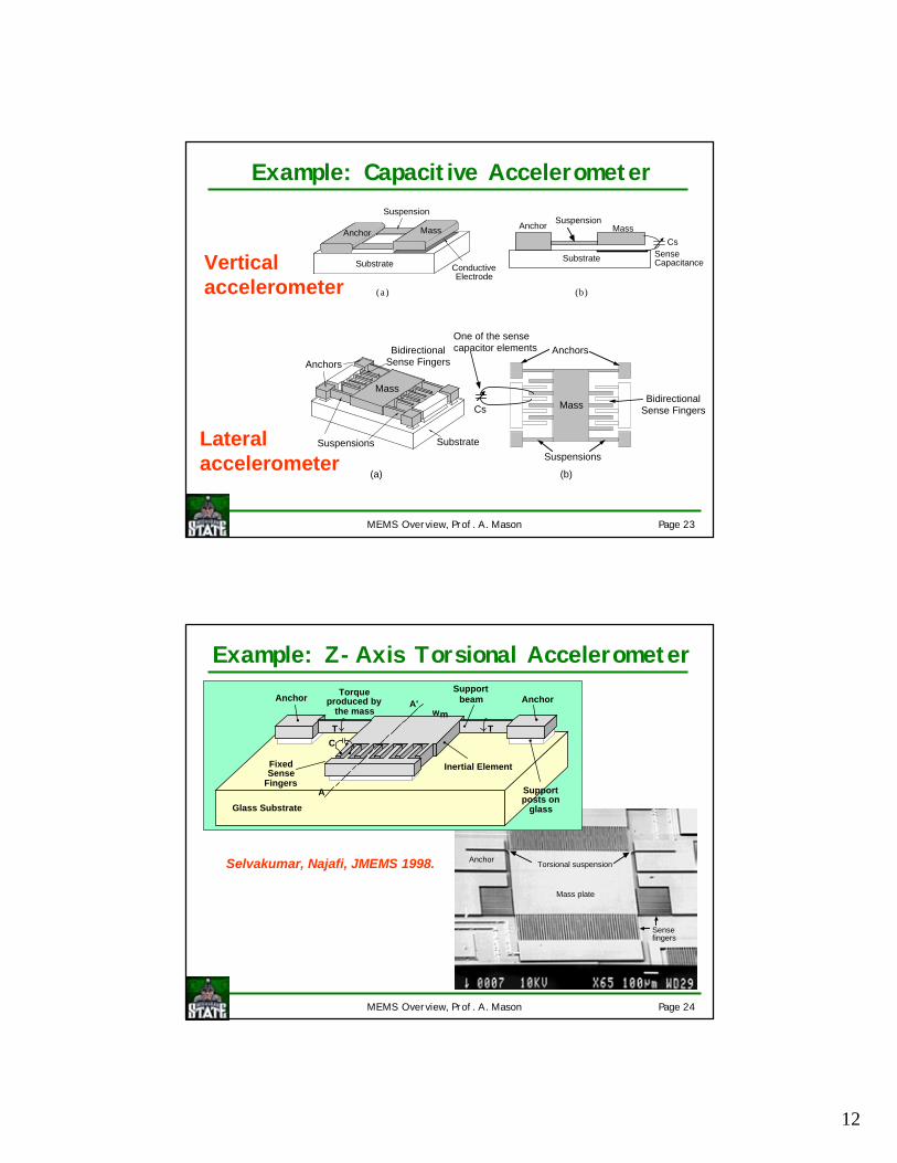
Example: Capacitive Accelerometer
Substrate
Mass
Suspension
Anchor
ConductiveElectrode
Cs
SuspensionMassAnchor
Substrate SenseCapacitance
(a) (b)
Verticalaccelerometer
Mass
Suspensions
BidirectionalSense Fingers
Substrate
Anchors
(a)
Mass
Anchors
Suspensions
BidirectionalSense Fingers
(b)
Cs
One of the sensecapacitor elements
Lateralaccelerometer
MEMS Overview, Prof. A. Mason Page 24
Example: Z-Axis Torsional Accelerometer
Selvakumar, Najafi, JMEMS 1998.
Mass plate
Sensefingers
Anchor Torsional suspension
C
FixedSense
Fingers
AnchorSupport
beam
Inertial Element
Torqueproduced by
the mass
T T
Glass Substrate
Supportposts on
glass
wm
A
A'Anchor
13
MEMS Overview, Prof. A. Mason Page 25
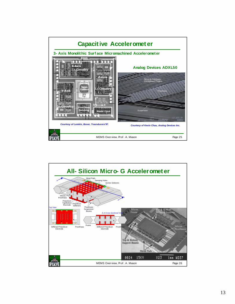
Capacitive Accelerometer
Courtesy of Lemkin, Boser, Trasnducers’97.
Analog Devices ADXL50
3-Axis Monolithic Surface Micromachined Accelerometer
Proofmass
Suspension
Sense & FeedbackInterdigitated Fingers
Courtesy of Kevin Chau, Analog Devices Inc.
MEMS Overview, Prof. A. Mason Page 26
All-Silicon Micro-G Accelerometer
PolysiliconTop/BottomElectrode
Damping HolesAnchor Dielectric
PolysiliconStiffeners
SiliconProofmass
A
A
Metal Pads
ProofmassSuspension
Beams
ProofmassStiffened PolysiliconElectrode
Frame
A-A Cross-Sectional View
Top View
ProofmassStiffened PolysiliconElectrode
14
MEMS Overview, Prof. A. Mason Page 27
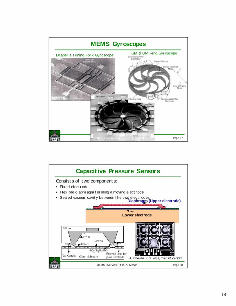
Draper’s Tuning Fork GyroscopePerforated
masses (tines)
DriveCombs
Suspension
MEMS GyroscopesGM & UM Ring Gyroscope
Electrodes
Ringstructure
MEMS Overview, Prof. A. Mason Page 28
Capacitive Pressure SensorsConsists of two components:• Fixed electrode• Flexible diaphragm forming a moving electrode • Sealed vacuum cavity between the two electrodes
Diaphragm (Upper electrode)
Lower electrode
Ti/Pt/Au
SiO2/Si3N4/SiO2Tab Contact
Silicon
Poly-Si
P++ Si
Glass SubstrateExternal lead forglass electrode A. Chavan, K.D. Wise, Transducers’97
15
MEMS Overview, Prof. A. Mason Page 29
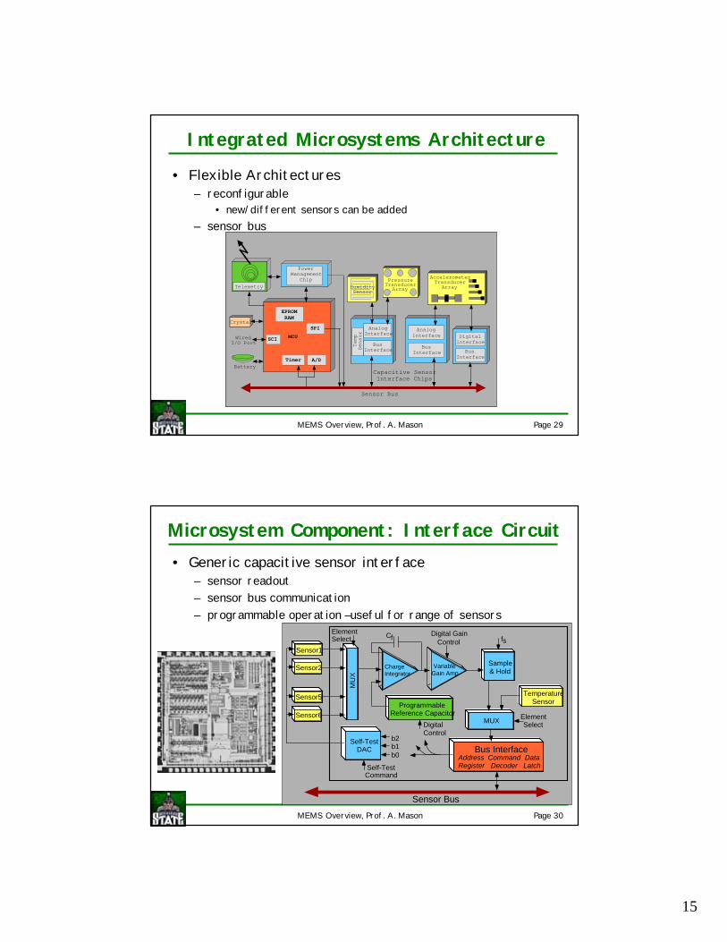
Integrated Microsystems Architecture
• Flexible Architectures– reconfigurable
• new/different sensors can be added– sensor bus
BusInterface
AnalogInterface
BusInterface
DigitalInterface
PressureTransducer
Array
BusInterface
AnalogInterface
AccelerometerTransducer
Array
MCU
SPI
EPROMRAM
WiredI/O Port
Capacitive SensorInterface Chips
SCI
Timer A/DBattery
Sensor Bus
PowerManagement
Chip
Telemetry HumiditySensor
Crystal
Temp
Sensor
MEMS Overview, Prof. A. Mason Page 30
Microsystem Component: Interface Circuit• Generic capacitive sensor interface
– sensor readout– sensor bus communication– programmable operation –useful for range of sensors
Digital GainControl
Self-TestCommand
b2b1b0
ElementSelect
ElementSelect
Sensor Bus
Cf
DigitalControl
fs
Bus InterfaceAddressRegister
CommandDecoder
DataLatch
MUX
MU
X
TemperatureSensor
Sensor6
Sensor2
Sensor1
Self-TestDAC
Sample& Hold
ChargeIntegrator
VariableGain Amp
ProgrammableReference Capacitor
Sensor5
16
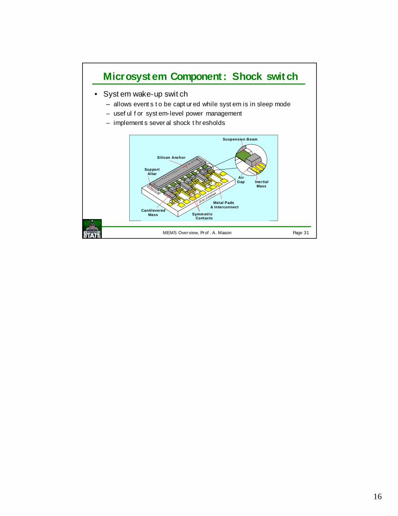
MEMS Overview, Prof. A. Mason Page 31
Microsystem Component: Shock switch• System wake-up switch
– allows events to be captured while system is in sleep mode– useful for system-level power management– implements several shock thresholds
CantileveredMass Symm etric
Contacts
SupportAltar
Metal Pads & Interconnect
Silicon Anchor
Iner tialMass
AirGap
Suspension Beam


![REPORT MEMS overview - Illinois Institute ofdatasys.cs.iit.edu/reports/2002_WSU_csc8800_2002.pdf · MEMS Technology Overview and Limitations CSC8800 Page 3 of 22 example [12]. SEMATECH,](https://img.pdfslide.us/doc/110x75/5a95128c7f8b9a30358c6db4/report-mems-overview-illinois-institute-technology-overview-and-limitations-csc8800.jpg)