Embed Size (px)
Citation preview


MeMO
Memory Mechanisms in Oxides
AnalogicMemoryArtificialNeurons (AMAN)
MeMO -> MeMOLogic <-MemoryAggresiveEnvironmets (MAGEN)
MeMOSatAhoRRAM


-60 -40 -20 0 20 40 600.0
0.1
0.2
0.3
0.4
0.5
0.6
0.7
0.8
0.9
IN, O
UT:
V (V
)
t (S)
-2
-1
0
1
2
3
4
5
6
VC
Q3:
V (V
)
“Analog memory devices”
120000 cycles
GomezMarlasca et al., APL 98, 123502 (2011).
“Asymmetric pulsing for reliableoperation of titanium/manganite memristors”
GomezMarlasca et al., APL.98, 042901(2011)
“Understanding Electroformingin Bipolar Resistive Switching Oxides”
Dispositivos con Memoria No VolDispositivos con Memoria No Voláátil til ReRAMReRAM = = ResistiveResistive RAM /2011RAM /2011
@GIA-CAC: Levy, Stoliar, Rubí, GMarlasca, Ghenzi, Leyva, Albornoz.@utside: Rozenberg (UBA), Sánchez(CAB).
1) usando 1) usando manganitasmanganitas policristalinaspolicristalinas

1) usando 1) usando manganitasmanganitas policristalinas / policristalinas / BiFeOBiFeODispositivos con Memoria No VolDispositivos con Memoria No Voláátil til ReRAMReRAM = = ResistiveResistive RAM /2011RAM /2011
@GIA-CAC: Levy, Stoliar, Rubí, GMarlasca, Ghenzi.@utside: Rozenberg (UBA), Sánchez(CAB).
Optimization of resistive switchingperformance of metal-manganite oxide interfaces by a multipulse protocolGhenzi et al, submited (2012)
Electronic transport mechanismsin metal-manganite memristive
interfaces,F.GMarlasca et al, submited (2012)
Resistive Switching in Bi0.9Ca0.1FeO3,Rubí et al., submited (2012)
100 200
150
160
170
180
Res
ista
nce
(MΩ
)
Time (s)
-800
-600
-400
-200
0
200
(a)
Stimulus (V)
100 200 300 400
140
160
180
200
Res
ista
nce
(MΩ
)
Time (s)
-800
-600
-400
-200
0
200
Stimulus (V)
(b)

poly TiO2-x/ Sidip coating by GSolerIllia et al.
N.Ghenzi et al, Physica B (2011)
0.0 0.5 1.0
0.0
0.5
1.0
1.5
I [m
A]
V [V]
SET
reset
0 2 4 6 8 10 12 14 16 18-0.20.00.20.40.60.81.01.21.41.6
Vset Vreset
V [V
]
Cycle number
TiO2 by reactive sputtering @ INTI
Ag (hand paint)TiO2 (~90 nm)AuCrNSiSi
0 2000 4000 6000 80001
10
100
I_R
EM
@ 0
.1 V
(uA
) a
fter +
/- 10
V P
ulse
s# pulse
Ag-poly TiO2-x/ Si(dip coating)
Stoliar, Ghenzi et al.
+ litho @ salaLimpiaMEMS-CAC
TiO2 sputtering @MEMS-CAC+ ex-situ oxidation
-Ti 20 nm-TiO2 20 nm-Au 80 nm
2) usando 2) usando TiOTiO22
Dispositivos con Memoria No VolDispositivos con Memoria No Voláátil til ReRAMReRAM = = ResistiveResistive RAM /2011RAM /2011
@GIA-CAC: Levy, Stoliar, Rubí, GMarlasca, Ghenzi, Quinteros, Palumbo@utside GQ: GSoler et al., @MEMS:Bonaparte et al., @INTI:Fraigi, Malatto, Mangano

...primera etapa de miniaturización...!
@GIA-CAC: Ghenzi, Rubí, Stoliar, Levy@INTI: Mangano, Malatto, Fraigi
2) usando 2) usando TiOTiO22

2) usando 2) usando TiOTiO22
14 dispositivos testeados, 14 con RS...!!!!
device#14, 500 cycles, RoomT

3) 3) usandousando cupratoscupratos policristalinospolicristalinos
“Dynamical behaviour of the resistiveswitching in ceramic YBCO/metalinterfaces”
“Retentivity of RRAM Devices Basedon Metal / YBCO Interfaces”,
Dispositivos con Memoria No VolDispositivos con Memoria No Voláátil til ReRAMReRAM = = ResistiveResistive RAM /2011RAM /2011
A.Schulman and C.Acha, Proceedings MRS 2011C.Acha, J. Phys. D: Appl. Phys. 44 (2011) 345301
@Lab.BajasTemperaturas, DF, FCEN, UBA: Acha, Schulman,

Dispositivos con Memoria No VolDispositivos con Memoria No Voláátil til ReRAMReRAM = = ResistiveResistive RAM /2011RAM /2011
10 nm-thick HfO2 layerPt
Pt
@CAC-GIA Stoliar, Marlasca, Levy@UNSAM N.Quintieri, P. Díaz Vélez, D.Quisbert@nanoGUNE, F.Golmar, Stoliar, Hueso
@CAC-GIA Palumbo@UABarcelona, E.Miranda@LETI, Grenoble: Ghibaudo, Jousseaume
5) 5) samplessamples @broad@broadHfOHfOHfOHfO
MgOMgO@CAC-GIA F.GMarlasca, P.Levy@IBM-Almaden, S.Parkin, JaeWoo Jeong


MeMOTrabajo experimental / instituciones
CONICE
T
LBT
FCEN- UBAMicroelectrónica
INTI
MicroLab
ECyT-UNSAM
LPEyM /
LID /MEMS
CAC-CNEA

MeMoLógica®
RXR(T,H)M(T,H)AFM
Mechanism Simulations Polycristals ThinFilms Electrodes
Downscaling and packaging: Proof of Concept PoC
PoP: PROOF OF PRINCIPLE LogicMaterial Impl
NeuralNetworkMeMO @ AGresive ENvironments
(( MAGEN ))
CHARACTERIZATION
MeMO
PRESENTADO A PICT BICENTENARIO: NO EVALUADO POR FALTA DE FIRMAS DE INVS….

Materiales: LPCMO, YBCO, TiO_1, TiO_2, TiO_3, LCMO, BiFeO, HfO
Instrumentación y procesamiento microfabricaciòn
NUEVAS IDEAS…

MeMOPerspectivas y Nuevos desafíos...

ResistiveSwitching…Type I: filamentary type ~nonpolar
~binary oxidesNiO2, TiO2, …………...
RS in TMO, A Sawa, Materials Today 11, 28 (2008)

Type II - interface type~bipolar…Resistive Switching
~“complex” oxides… SrTiO, SrZrO, … perovskites (CMR, HTcS)
RS in TMO, A Sawa, Materials Today 11, 28 (2008)
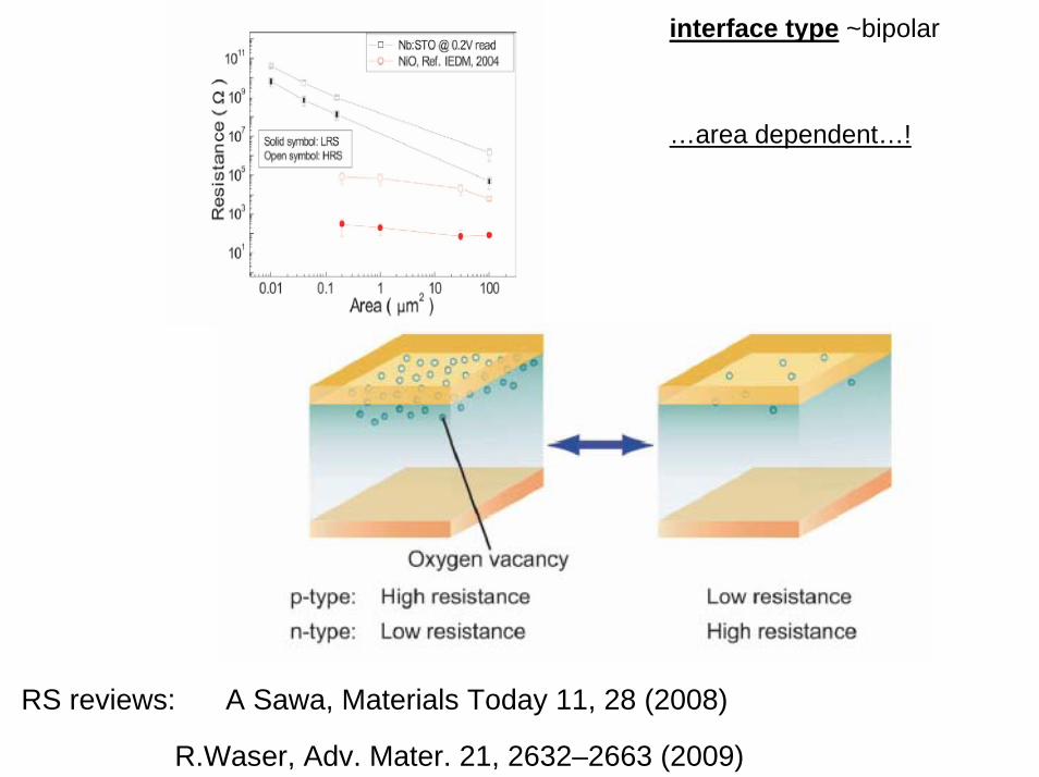
interface type ~bipolar
…area dependent…!
RS reviews: A Sawa, Materials Today 11, 28 (2008)
R.Waser, Adv. Mater. 21, 2632–2663 (2009)

La1-xCaxMnO3
PS
Room T and above
No influence of LT ordering…!
e- transport in ManganitesConduction through Double Exchange Mn+3 - O - Mn+4Mn-O-Mn bonds allow eg to move from Mn+3 to Mn+4
Mn-O bonds disrupted ⇒ R increases …!…role of vacancies…
La5/8-yPryCa3/8MnO3 polycristalline samples
Simultaneous electric and magnetic field induced non-volatile memory Quintero, Leyva and PL, APL86, 242102 (2005).

0.028 0.278 2.778 27.778
0.01
0.1
PLCMO (Pr=0.3) T=300 K
A B C D
VBD
(V)
Time (hours...!)
24.4 24.6 24.8 25.0 25.2 25.4 25.6 25.80.0
0.1
V10
2
Time (hours)
0.00
0.05
V10
3
1x10⁻⁴
2x10⁻⁴
2x10⁻⁴
PLCMO Pr=0.3 T=300 K i = 1mA
V10
1
high retention time
I I
A B C D
AD → pulses
AD → bias I
amplitude…
1 2 3 4 5 6 7 8 9 10 110
5
10
15
20
25
LP(03)CMO T = 300 K pulse time (2 ms, 2ms)20 pulses
EPIR
(%)
V (Volts)
1E-3
0.01
0.1
VA
C (V
)1000 2000 3000 4000 5000 6000 7000 8000 9000 10000
0.01
as
time (sec.)
VB
D(V
)0 50 100 150 200 250
0.00480.00510.0054
# pulses
~ 300 %
~ 10 %
0.00
0.05
0.10
VB
D
VA
C
accumulative..!!
http://www.tandar.cnea.gov.ar/doctorado/Tesis/Quintero.pdf
Ag/ poly La0.375Pr0.300 Ca0.325MnO3 at RoomT

Hysteresis
Switching
Loop
I-V standard curves“dynamic response”
Prot
ocol
Dyn
and
Rem
DA
TA

Ag / poly La0.375Pr0.300 Ca0.325MnO3
A B C D
- +
o--
A B C D
+ -
o--
O vacanciesdisrupt Double
Exchange transport
during the pulse...
AD → pulses
AD → bias I
HIGH r
low r
after the pulse...
Com
plem
enta
ry
NonVolatile...!
Mec
hani
sm
+
GomezMarlasca & PL, J. Phys.: Conf. Ser. 167, 012036 (2009)

Dynamic resistance ( I-V)
A B C D
+ -
o--
Single contact
Remnant resistance
Hysteresis
Switching
Loop
Note HUGE changes in Rdynwhile Rrem is ~ constant
FGM and PL, J. Phys.: Conf. Ser. 167, 012036 (2009)

…una foto del estado de producción en abril de 2010
---theoretical(SIMULATORS: Rozenberg, Sánchez
---experimental (EXPTLS: Levy, Quintero, GMarlasca
---experimental (EXPTLS: Acha,
---theo+exptl
H.Yi, T. Choi and Sang-Wook Cheong, Abstract: P37.00010 : "Reversible Resistive Switching in (La,Pr,Ca)MnO3; Cryogenic nonvolatile RAM", http://meetings.aps.org/Meeting/MAR10/Event/120506 ; APL(2010)

---theoretical(SIMULATORS: Rozenberg, Sánchez
---experimental (EXPTLS: Levy, Quintero, GMarlasca
---experimental (EXPTLS: Acha,
---theo+exptl
Phys.B(2011)
APL(2011)
Assymetric…APL(2011)
Multipulse….JAP(2012)
BiFeO…PhysB(2011)
MLC….to be submited…

MeMoLógica®
RXR(T,H)M(T,H)AFM
Mechanism Simulations Polycristals ThinFilms Electrodes
Downscaling and packaging: Proof of Concept PoC
PoP: PROOF OF PRINCIPLE LogicMaterial Impl
NeuralNetworkMeMO @ AGresive ENvironments
(( MAGEN ))
CHARACTERIZATION
MeMO
mayo2010
MeMO
MeMO

MeMoLógica®
RXR(T,H)M(T,H)AFM
Mechanism Simulations Polycristals ThinFilms Electrodes
Downscaling and packaging: Proof of Concept PoC
PoP: PROOF OF PRINCIPLE LogicMaterial Impl
NeuralNetworkMeMO @ AGresive ENvironments
(( MAGEN ))
CHARACTERIZATION
MeMO
MeMO MeMOMeMO
MeMO
MeMO
MeMO
MeMO
MeMO
MeMO
MeMO
MeMO
MeMO
MeMO
MeMO
DIC 2011